US11520429B2 - Three-dimensional sensing module and method of manufacturing the same and electronic apparatus - Google Patents

Three-dimensional sensing module and method of manufacturing the same and electronic apparatus Download PDF

Info

Publication number
US11520429B2
US11520429B2 US17/011,108 US202017011108A US11520429B2 US 11520429 B2 US11520429 B2 US 11520429B2 US 202017011108 A US202017011108 A US 202017011108A US 11520429 B2 US11520429 B2 US 11520429B2
Authority
US
United States
Prior art keywords
electrode layer
spacer layer
functional spacer
light
layer
Prior art date
Legal status (The legal status is an assumption and is not a legal conclusion. Google has not performed a legal analysis and makes no representation as to the accuracy of the status listed.)
Active, expires
Application number
US17/011,108
Other versions
US20220066608A1 (en
Inventor
Lien Hsin Lee
Ren Hung Wang
Cai Jin Ye
Wei Yi Lin
Tai Shih Cheng
Tsai Kuei Wei
Chih Cheng Chuang
Sun Po Lin
Current Assignee (The listed assignees may be inaccurate. Google has not performed a legal analysis and makes no representation or warranty as to the accuracy of the list.)
TPK Advanced Solutions Inc
Original Assignee
TPK Advanced Solutions Inc
Priority date (The priority date is an assumption and is not a legal conclusion. Google has not performed a legal analysis and makes no representation as to the accuracy of the date listed.)
Filing date
Publication date
Application filed by TPK Advanced Solutions Inc filed Critical TPK Advanced Solutions Inc
Priority to US17/011,108 priority Critical patent/US11520429B2/en
Assigned to TPK ADVANCED SOLUTIONS INC. reassignment TPK ADVANCED SOLUTIONS INC. ASSIGNMENT OF ASSIGNORS INTEREST (SEE DOCUMENT FOR DETAILS). Assignors: YE, CAI JIN, LEE, LIEN HSIN, WANG, REN HUNG, CHENG, TAI SHIH, LIN, WEI YI, CHUANG, CHIH CHENG, LIN, SUN PO, WEI, TSAI KUEI
Publication of US20220066608A1 publication Critical patent/US20220066608A1/en
Application granted granted Critical
Publication of US11520429B2 publication Critical patent/US11520429B2/en
Active legal-status Critical Current
Adjusted expiration legal-status Critical

Links

Images

Classifications

    • GPHYSICS
    • G06COMPUTING OR CALCULATING; COUNTING
    • G06FELECTRIC DIGITAL DATA PROCESSING
    • G06F3/00Input arrangements for transferring data to be processed into a form capable of being handled by the computer; Output arrangements for transferring data from processing unit to output unit, e.g. interface arrangements
    • G06F3/01Input arrangements or combined input and output arrangements for interaction between user and computer
    • G06F3/03Arrangements for converting the position or the displacement of a member into a coded form
    • G06F3/041Digitisers, e.g. for touch screens or touch pads, characterised by the transducing means
    • G06F3/0414Digitisers, e.g. for touch screens or touch pads, characterised by the transducing means using force sensing means to determine a position
    • G06F3/04146Digitisers, e.g. for touch screens or touch pads, characterised by the transducing means using force sensing means to determine a position using pressure sensitive conductive elements delivering a boolean signal and located between crossing sensing lines, e.g. located between X and Y sensing line layers
    • GPHYSICS
    • G01MEASURING; TESTING
    • G01LMEASURING FORCE, STRESS, TORQUE, WORK, MECHANICAL POWER, MECHANICAL EFFICIENCY, OR FLUID PRESSURE
    • G01L1/00Measuring force or stress, in general
    • G01L1/20Measuring force or stress, in general by measuring variations in ohmic resistance of solid materials or of electrically-conductive fluids; by making use of electrokinetic cells, i.e. liquid-containing cells wherein an electrical potential is produced or varied upon the application of stress
    • G01L1/205Measuring force or stress, in general by measuring variations in ohmic resistance of solid materials or of electrically-conductive fluids; by making use of electrokinetic cells, i.e. liquid-containing cells wherein an electrical potential is produced or varied upon the application of stress using distributed sensing elements
    • GPHYSICS
    • G01MEASURING; TESTING
    • G01LMEASURING FORCE, STRESS, TORQUE, WORK, MECHANICAL POWER, MECHANICAL EFFICIENCY, OR FLUID PRESSURE
    • G01L1/00Measuring force or stress, in general
    • G01L1/20Measuring force or stress, in general by measuring variations in ohmic resistance of solid materials or of electrically-conductive fluids; by making use of electrokinetic cells, i.e. liquid-containing cells wherein an electrical potential is produced or varied upon the application of stress
    • G01L1/22Measuring force or stress, in general by measuring variations in ohmic resistance of solid materials or of electrically-conductive fluids; by making use of electrokinetic cells, i.e. liquid-containing cells wherein an electrical potential is produced or varied upon the application of stress using resistance strain gauges
    • G01L1/2287Measuring force or stress, in general by measuring variations in ohmic resistance of solid materials or of electrically-conductive fluids; by making use of electrokinetic cells, i.e. liquid-containing cells wherein an electrical potential is produced or varied upon the application of stress using resistance strain gauges constructional details of the strain gauges
    • GPHYSICS
    • G06COMPUTING OR CALCULATING; COUNTING
    • G06FELECTRIC DIGITAL DATA PROCESSING
    • G06F3/00Input arrangements for transferring data to be processed into a form capable of being handled by the computer; Output arrangements for transferring data from processing unit to output unit, e.g. interface arrangements
    • G06F3/01Input arrangements or combined input and output arrangements for interaction between user and computer
    • G06F3/03Arrangements for converting the position or the displacement of a member into a coded form
    • G06F3/041Digitisers, e.g. for touch screens or touch pads, characterised by the transducing means
    • G06F3/044Digitisers, e.g. for touch screens or touch pads, characterised by the transducing means by capacitive means
    • G06F3/0445Digitisers, e.g. for touch screens or touch pads, characterised by the transducing means by capacitive means using two or more layers of sensing electrodes, e.g. using two layers of electrodes separated by a dielectric layer
    • GPHYSICS
    • G06COMPUTING OR CALCULATING; COUNTING
    • G06FELECTRIC DIGITAL DATA PROCESSING
    • G06F3/00Input arrangements for transferring data to be processed into a form capable of being handled by the computer; Output arrangements for transferring data from processing unit to output unit, e.g. interface arrangements
    • G06F3/01Input arrangements or combined input and output arrangements for interaction between user and computer
    • G06F3/03Arrangements for converting the position or the displacement of a member into a coded form
    • G06F3/041Digitisers, e.g. for touch screens or touch pads, characterised by the transducing means
    • G06F3/044Digitisers, e.g. for touch screens or touch pads, characterised by the transducing means by capacitive means
    • G06F3/0446Digitisers, e.g. for touch screens or touch pads, characterised by the transducing means by capacitive means using a grid-like structure of electrodes in at least two directions, e.g. using row and column electrodes
    • GPHYSICS
    • G06COMPUTING OR CALCULATING; COUNTING
    • G06FELECTRIC DIGITAL DATA PROCESSING
    • G06F2203/00Indexing scheme relating to G06F3/00 - G06F3/048
    • G06F2203/041Indexing scheme relating to G06F3/041 - G06F3/045
    • G06F2203/04102Flexible digitiser, i.e. constructional details for allowing the whole digitising part of a device to be flexed or rolled like a sheet of paper
    • GPHYSICS
    • G06COMPUTING OR CALCULATING; COUNTING
    • G06FELECTRIC DIGITAL DATA PROCESSING
    • G06F2203/00Indexing scheme relating to G06F3/00 - G06F3/048
    • G06F2203/041Indexing scheme relating to G06F3/041 - G06F3/045
    • G06F2203/04103Manufacturing, i.e. details related to manufacturing processes specially suited for touch sensitive devices
    • GPHYSICS
    • G06COMPUTING OR CALCULATING; COUNTING
    • G06FELECTRIC DIGITAL DATA PROCESSING
    • G06F2203/00Indexing scheme relating to G06F3/00 - G06F3/048
    • G06F2203/041Indexing scheme relating to G06F3/041 - G06F3/045
    • G06F2203/04106Multi-sensing digitiser, i.e. digitiser using at least two different sensing technologies simultaneously or alternatively, e.g. for detecting pen and finger, for saving power or for improving position detection

Definitions

  • the present disclosure relates to a three-dimensional sensing module and a method of manufacturing the same and an electronic apparatus.
  • touch modules have been maturely applied to industrial electronics and consumer electronics products.
  • Demand has progressed from determining the two-dimensional position (e.g., the X-axis direction and the Y-axis direction) of the touch point on the surface of the screen to also sensing the force parameter caused by the change of the force applied to the surface of the screen (e.g., the Z-axis direction).
  • the force parameter caused by the change of the force applied to the surface of the screen (e.g., the Z-axis direction).
  • the conventional technology proposed by the existing industry has the following problems in the pressure sensor mounted on the touch module: (1) the X-Y-Z three-axis electrodes cannot have flexible characteristics at the same time and cannot be used as a flexible assembly; and (2) only a partial area has the Z-axis sensing function.
  • An aspect of the disclosure is to provide a three-dimensional sensing module that can efficiently solve the aforementioned problems.
  • a three-dimensional sensing module includes a touch pressure sensing structure.
  • the touch pressure sensing structure includes a first functional spacer layer, a first light-transmitting electrode layer, a second functional spacer layer, a second light-transmitting electrode layer, and a third functional spacer layer.
  • the first light-transmitting electrode layer is coated on the first functional spacer layer.
  • the second functional spacer layer is coated on the first light-transmitting electrode layer.
  • the second light-transmitting electrode layer is coated on the second functional spacer layer.
  • the third functional spacer layer is coated on the second light-transmitting electrode layer. Resistivities of the first functional spacer layer, the second functional spacer layer, and the third functional spacer layer are greater than resistivities of the first light-transmitting electrode layer and the second light-transmitting electrode layer.
  • the touch pressure sensing structure further includes a first flexible touch electrode layer and a second flexible touch electrode layer.
  • the first functional spacer layer is coated on the first flexible touch electrode layer.
  • the second flexible touch electrode layer is coated on the third functional spacer layer.
  • the three-dimensional sensing module further includes a flexible cover plate disposed on the second flexible touch electrode layer.
  • the three-dimensional sensing module further includes a controller configured to detect a touch position signal and a pressure sensing signal through the first flexible touch electrode layer and the second flexible touch electrode layer.
  • At least one of the first flexible touch electrode layer, the first light-transmitting electrode layer, the second light-transmitting electrode layer, or the second flexible touch electrode layer is a silver nanowire electrode layer.
  • resistivities of the first flexible touch electrode layer and the second flexible touch electrode layer range from 1 Ops to 150 Ops.
  • the resistivities of the first light-transmitting electrode layer and the second light-transmitting electrode layer range from 150 Ops to 500 Ops.
  • the resistivity of the second functional spacer layer ranges from 500 Ops to 1000 Ops.
  • the resistivities of the first functional spacer layer and the third functional spacer layer range from 800 Ops to 1200 Ops.
  • thicknesses of the first functional spacer layer and the third functional spacer layer are substantially the same.
  • a thickness of the second functional spacer layer is smaller than the thickness of at least one of the first functional spacer layer or the third functional spacer layer.
  • the thickness of the second functional spacer layer ranges from 30 nm to 100 nm.
  • the thicknesses of the first functional spacer layer and the third functional spacer layer range from 400 nm to 1200 nm.
  • each of the first light-transmitting electrode layer and the second light-transmitting electrode layer includes a plurality of electrode blocks spaced apart from each other.
  • At least one of the first functional spacer layer, the second functional spacer layer, or the third functional spacer layer is a substrate layer doped with a low-concentration of silver nanowires.
  • an electronic apparatus includes the three-dimensional sensing module and a display module.
  • the display module is disposed under the three-dimensional sensing module.
  • a method of manufacturing a three-dimensional sensing module includes: forming a first flexible touch electrode layer; coating a light-transmitting force-sensitive composite layer on the first flexible touch electrode layer, in which the light-transmitting force-sensitive composite layer includes at least one light-transmitting electrode layer and at least one functional spacer layer, and a resistivity of the at least one light-transmitting electrode layer is smaller than a resistivity of the at least one functional spacer layer; and coating a second flexible touch electrode layer on the light-transmitting force-sensitive composite layer.
  • the coating the light-transmitting force-sensitive composite layer includes: coating a first functional spacer layer on the first flexible touch electrode layer; coating a first light-transmitting electrode layer on the first functional spacer layer; coating a second functional spacer layer on the first light-transmitting electrode layer; coating a second light-transmitting electrode layer on the second functional spacer layer; and coating a third functional spacer layer on the second light-transmitting electrode layer.
  • the touch pressure sensing structure is formed by two flexible touch electrode layers and a light-transmitting force-sensitive composite layer stacked therebetween, so as to provide a two-dimensional touch position signal and a third-dimensional pressure sensing signal at the same time.
  • the three-dimensional sensing module of the present disclosure can be simply completed by only multiple coating processes. Therefore, compared with the conventional complicated method of separately manufacturing the touch module and the display module and then gluing them, the manufacturing process of the three-dimensional sensing module of the present disclosure can completely eliminate the use of glue. As a result, the multi-layer gluing process and the thickness of the glue can be reduced, so that the three-dimensional sensing module of the present disclosure can realize a thin design.
  • FIG. 1 is a schematic diagram of an electronic apparatus according to an embodiment of the disclosure
  • FIG. 2 is a partial view of some components of the electronic apparatus in
  • FIG. 1 is a diagrammatic representation of FIG. 1 ;
  • FIG. 3 A is a partial enlarged view of a light-transmitting force-sensitive composite layer in FIG. 1 that is not pressed;
  • FIG. 3 B is a partial enlarged view of the light-transmitting force-sensitive composite layer in FIG. 1 that is pressed;
  • FIG. 4 is a schematic diagram of an electronic apparatus according to another embodiment of the disclosure.
  • FIG. 5 is a flowchart of a method of manufacturing a three-dimensional sensing module according to an embodiment of the disclosure.
  • FIG. 1 is a schematic diagram of an electronic apparatus 100 according to an embodiment of the disclosure.
  • FIG. 2 is a partial view of some components of the electronic apparatus 100 in FIG. 1 .
  • the electronic apparatus 100 of the present embodiment is a touch display device as an example and includes a three-dimensional sensing module 110 and a display module 120 .
  • the display module 120 is disposed under the three-dimensional sensing module 110 .
  • the three-dimensional sensing module 110 includes a touch pressure sensing structure 111 and a flexible cover plate 112 .
  • the touch pressure sensing structure 111 includes a first flexible touch electrode layer 111 a 1 , a second flexible touch electrode layer 111 a 2 , and a light-transmitting force-sensitive composite layer 111 b located between the first flexible touch electrode layer 111 a 1 and the second flexible touch electrode layer 111 a 2 .
  • the light-transmitting force-sensitive composite layer 111 b includes a first functional spacer layer 111 b 11 , a first light-transmitting electrode layer 111 b 21 , a second functional spacer layer 111 b 12 , a second light-transmitting electrode layer 111 b 22 , and a third functional spacer layer 111 b 13 .
  • the first functional spacer layer 111 b 11 is coated on the first flexible touch electrode layer 111 a 1 .
  • the first light-transmitting electrode layer 111 b 21 is coated on the first functional spacer layer 111 b 11 .
  • the second functional spacer layer 111 b 12 is coated on the first light-transmitting electrode layer 111 b 21 .
  • the second light-transmitting electrode layer 111 b 22 is coated on the second functional spacer layer 111 b 12 .
  • the third functional spacer layer 111 b 13 is coated on the second light-transmitting electrode layer 111 b 22 . Resistivities of the first functional spacer layer 111 b 11 , the second functional spacer layer 111 b 12 , and the third functional spacer layer 111 b 13 are greater than resistivities of the first light-transmitting electrode layer 111 b 21 and the second light-transmitting electrode layer 111 b 22 .
  • the second flexible touch electrode layer 111 a 2 is coated on the third functional spacer layer 111 b 13 .
  • the flexible cover plate 112 is disposed on the second flexible touch electrode layer 111 a 2 .
  • the material of the flexible cover plate 112 includes a flexible polymer material.
  • the flexible polymer material includes Colorless Polyimide (PI), but the present disclosure is not limited in this regard.
  • the three-dimensional sensing module 110 further includes a controller 113 .
  • the controller 113 is electrically connected to the first flexible touch electrode layer 111 a 1 and the second flexible touch electrode layer 111 a 2 .
  • both the first flexible touch electrode layer 111 a 1 and the second flexible touch electrode layer 111 a 2 are electrode layers after patterning, and the patterns are only for illustration and not intended to limit the scope of the present disclosure.
  • the principle of the controller 113 to detect the touch position signal via the first flexible touch electrode layer 111 a 1 and the second flexible touch electrode layer 111 a 2 will not be described in detail here, and the related art can be referred to.
  • At least one of the first flexible touch electrode layer 111 a 1 , the first light-transmitting electrode layer 111 b 21 , the second light-transmitting electrode layer 111 b 22 , or the second flexible touch electrode layer 111 a 2 can be a silver nanowire electrode layer (SNW; also known as AgNW), a metal grid, or an indium tin oxide (ITO) electrode layer, but the present disclosure is not limited in this regard.
  • SNW silver nanowire electrode layer
  • ITO indium tin oxide
  • the light-transmitting force-sensitive composite layer 111 b has an optical transmittance greater than 85% and a haze less than 3%.
  • at least one of the first light-transmitting electrode layer 111 b 21 or the second light-transmitting electrode layer 111 b 22 is a silver nanowire electrode layer.
  • FIG. 3 A is a partial enlarged view of a light-transmitting force-sensitive composite layer 111 b in FIG. 1 that is not pressed.
  • each of the first light-transmitting electrode layer 111 b 21 and the second light-transmitting electrode layer 111 b 22 includes a substrate and silver nanowires doped therein.
  • the silver nanowires overlap each other in the substrate to form a conductive network.
  • the substrate refers to a non-nanosilver material formed by a solution including the silver nanowires through processes such as coating, heating, and drying.
  • the silver nanowires are distributed or embedded in the substrate and partially protrude out from the substrate.
  • the substrate can protect the silver nanowires from the external environment, such as to protect against corrosion and abrasion.
  • the substrate is compressible.
  • a wire length of the silver nanowires ranges from about 10 ⁇ m to about 300 ⁇ m. In some embodiments, a wire diameter (or a wire width) of the silver nanowires is less than about 500 nm. In some embodiments, the silver nanowires can be deformed forms such as other conductive metal nanowires or non-conductive nanowires coated with silver. The use of the silver nanowires to form the silver nanowire electrode layers has the following advantages compared with ITO: low price, simple process, good flexibility, resistance to bending, and etc.
  • the first functional spacer layer 111 b 11 , the second functional spacer layer 111 b 12 , and the third functional spacer layer 111 b 13 can be light-transmitting coatings.
  • at least one of the first functional spacer layer 111 b 11 , the second functional spacer layer 111 b 12 , or the third functional spacer layer 111 b 13 can be a substrate layer doped with a low-concentration of silver nanowires.
  • each of the first functional spacer layer 111 b 11 , the second functional spacer layer 111 b 12 , and the third functional spacer layer 111 b 13 includes a substrate layer doped with a low-concentration of silver nanowires, so that resistivities of the first functional spacer layer 111 b 11 , the second functional spacer layer 111 b 12 , and the third functional spacer layer 111 b 13 are greater than resistivities of the first light-transmitting electrode layer 111 b 21 and the second light-transmitting electrode layer 111 b 22 , and the first functional spacer layer 111 b 11 , the second functional spacer layer 111 b 12 , and the third functional spacer layer 111 b 13 have greater optical transmittances.
  • the substrates of the first functional spacer layer 111 b 11 , the second functional spacer layer 111 b 12 , and the third functional spacer layer 111 b 13 are identical to the substrates of the first light-transmitting electrode layer 111 b 21 and the second light-transmitting electrode layer 111 b 22 , but the present disclosure is not limited in this regard.
  • the resistivities of the first flexible touch electrode layer 111 a 1 and the second flexible touch electrode layer 111 a 2 range from 1 Ops (Ohm per Square) to 150 Ops (preferably 60 Ops), but the present disclosure is not limited in this regard.
  • the resistivities of the first light-transmitting electrode layer 111 b 21 and the second light-transmitting electrode layer 111 b 22 range from 150 Ops to 500 Ops (preferably 300 Ops), but the present disclosure is not limited in this regard.
  • the resistivity of the second functional spacer layer 111 b 12 ranges from 500 Ops to 1000 Ops (preferably 600 Ops), but the present disclosure is not limited in this regard.
  • the resistivities of the first functional spacer layer 111 b 11 and the third functional spacer layer 111 b 13 range from 800 Ops to 1200 Ops (preferably 800 Ops), but the present disclosure is not limited in this regard.
  • the resistivity can be measured to verify whether the concentration of the doped silver nanowires is high (e.g., the first light-transmitting electrode layer 111 b 21 and the second light-transmitting electrode layer 111 b 22 ) or low (e.g., the first functional spacer layer 111 b 11 , the second functional spacer layer 111 b 12 , and the third functional spacer layer 111 b 13 ).
  • the difference in resistivity is related to the thickness.
  • FIG. 3 B is a partial enlarged view of the light-transmitting force-sensitive composite layer 111 b in FIG. 1 that is pressed.
  • the first light-transmitting electrode layer 111 b 21 and the second light-transmitting electrode layer 111 b 22 are made of silver nanowires, when an external pressing force from the side of the flexible cover plate 112 is transmitted to the light-transmitting force-sensitive composite layer 111 b , the first light-transmitting electrode layer 111 b 21 and the second light-transmitting electrode layer 111 b 22 will be compressed by the force to cause the silver nanowires inside to approach and pass through the first functional spacer layer 111 b 11 , the second functional spacer layer 111 b 12 , and the third functional spacer layer 111 b 13 .
  • the overall conductivity of the light-transmitting force-sensitive composite layer 111 b is improved (i.e., the resistivity decreases).
  • the silver nanowire L 1 in the first light-transmitting electrode layer 111 b 21 and the silver nanowire L 2 in the second functional spacer layer 111 b 12 do not contact each other.
  • FIG. 3 A when the light-transmitting force-sensitive composite layer 111 b has not been pressed, the silver nanowire L 1 in the first light-transmitting electrode layer 111 b 21 and the silver nanowire L 2 in the second functional spacer layer 111 b 12 do not contact each other.
  • the controller 113 can calculate the value of the external pressing force.
  • the value of the external pressing force can be calculated by the change in resistivity of the light-transmitting force-sensitive composite layer 111 b.
  • the controller 113 can simultaneously detect the touch position signal and the pressure sensing signal. In some other embodiments, the controller 113 can sequentially detect the touch position signal and the pressure sensing signal.
  • a thickness of the second functional spacer layer 111 b 12 ranges from about 30 nm to about 100 nm (preferably from about 40 nm to about 80 nm).
  • the resistivity between the light-transmitting force-sensitive composite layer 111 b and the first flexible touch electrode layer 111 a 1 and the second flexible touch electrode layer 111 a 2 can be increased. Therefore, when the controller 113 detects the touch position signal, the capacitive sensing signal obtained through the first flexible touch electrode layer 111 a 1 and the second flexible touch electrode layer 111 a 2 is not easily interfered with by the light-transmitting force-sensitive composite layer 111 b and is clearer.
  • each of the first light-transmitting electrode layer 111 b 21 and the second light-transmitting electrode layer 111 b 22 of the light-transmitting force-sensitive composite layer 111 b is a monolithic structure and can provide a single-finger detection function, but the present disclosure is not limited in this regard.
  • FIG. 4 is a schematic diagram of an electronic apparatus 200 according to another embodiment of the disclosure.
  • the electronic apparatus 200 includes a three-dimensional sensing module 210 and a display module 120 .
  • the three-dimensional sensing module 210 includes a touch pressure sensing structure 211 and a flexible cover plate 112 .
  • the touch pressure sensing structure 211 includes a first flexible touch electrode layer 111 a 1 , a second flexible touch electrode layer 111 a 2 , and a light-transmitting force-sensitive composite layer 211 b located between the first flexible touch electrode layer 111 a 1 and the second flexible touch electrode layer 111 a 2 .
  • the light-transmitting force-sensitive composite layer 211 b includes a first functional spacer layer 111 b 11 , a first light-transmitting electrode layer 211 b 21 , a second functional spacer layer 111 b 12 , a second light-transmitting electrode layer 211 b 22 , and a third functional spacer layer 111 b 13 .
  • the electronic apparatus 200 of this embodiment is modified with respect to the first light-transmitting electrode layer 211 b 21 and the second light-transmitting electrode layer 211 b 22 .
  • each of the first light-transmitting electrode layer 211 b 21 and the second light-transmitting electrode layer 211 b 22 includes a plurality of electrode blocks.
  • the electrode blocks are spaced apart from each other.
  • the first light-transmitting electrode layer 111 b 21 and the second light-transmitting electrode layer 111 b 22 shown in FIG. 1 can be patterned, so as to obtain the first light-transmitting electrode layer 211 b 21 and the second light-transmitting electrode layer 211 b 22 including pluralities of electrode blocks as illustrated in FIG. 4 , respectively.
  • the controller 113 can achieve multi-finger detection.
  • FIG. 5 is a flowchart of a method of manufacturing a three-dimensional sensing module according to an embodiment of the disclosure. As shown in FIG. 5 , a method of manufacturing a three-dimensional sensing module includes steps S 101 to S 103 .
  • step S 101 a first flexible touch electrode layer is formed.
  • a light-transmitting force-sensitive composite layer is coated on the first flexible touch electrode layer, in which the light-transmitting force-sensitive composite layer includes at least one light-transmitting electrode layer and at least one functional spacer layer, and a resistivity of the light-transmitting electrode layer is smaller than a resistivity of the functional spacer layer.
  • step S 103 a second flexible touch electrode layer is coated on the light-transmitting force-sensitive composite layer.
  • step S 102 includes steps S 102 a to S 102 e.
  • step S 102 a a first functional spacer layer is coated on the first flexible touch electrode layer.
  • step S 102 b a first light-transmitting electrode layer is coated on the first functional spacer layer.
  • step S 102 c a second functional spacer layer is coated on the first light-transmitting electrode layer.
  • step S 102 d a second light-transmitting electrode layer is coated on the second functional spacer layer.
  • step S 102 e a third functional spacer layer is coated on the second light-transmitting electrode layer.
  • the coating processes in the foregoing steps include a spin coating process or a slit die coating, but the present disclosure is not limited in this regard.
  • a step of patterning the first light-transmitting electrode layer can be added between step S 102 b and step S 102 c
  • a step of patterning the second light-transmitting electrode layer can be added between step S 102 d and step S 102 e.
  • the touch pressure sensing structure is formed by two flexible touch electrode layers and a light-transmitting force-sensitive composite layer stacked therebetween, so as to provide a two-dimensional touch position signal and a third-dimensional pressure sensing signal at the same time.
  • the three-dimensional sensing module of the present disclosure can be simply completed by only multiple coating processes. Therefore, compared with the conventional complicated method of separately manufacturing the touch module and the display module and then gluing them, the manufacturing process of the three-dimensional sensing module of the present disclosure can completely eliminate the use of glue. As a result, the multi-layer gluing process and the thickness of the glue can be reduced, so that the three-dimensional sensing module of the present disclosure can realize a thin design.

Landscapes

  • Engineering & Computer Science (AREA)
  • Physics & Mathematics (AREA)
  • General Physics & Mathematics (AREA)
  • General Engineering & Computer Science (AREA)
  • Theoretical Computer Science (AREA)
  • Human Computer Interaction (AREA)
  • Position Input By Displaying (AREA)

Abstract

A three-dimensional sensing module includes a touch pressure sensing structure. The touch pressure sensing structure includes a first functional spacer layer, a first light-transmitting electrode layer coated on the first functional spacer layer, a second functional spacer layer coated on the first light-transmitting electrode layer, a second light-transmitting electrode layer coated on the second functional spacer layer, and a third functional spacer layer coated on the second light-transmitting electrode layer. Resistivities of the first, second, and third functional spacer layers are greater than resistivities of the first and second light-transmitting electrode layers.

Description

BACKGROUND Technical Field
The present disclosure relates to a three-dimensional sensing module and a method of manufacturing the same and an electronic apparatus.
Description of Related Art
With the diversified development of touch modules, touch modules have been maturely applied to industrial electronics and consumer electronics products. Demand has progressed from determining the two-dimensional position (e.g., the X-axis direction and the Y-axis direction) of the touch point on the surface of the screen to also sensing the force parameter caused by the change of the force applied to the surface of the screen (e.g., the Z-axis direction). Even the application requirements for flexible panels will be inevitable.
However, the conventional technology proposed by the existing industry has the following problems in the pressure sensor mounted on the touch module: (1) the X-Y-Z three-axis electrodes cannot have flexible characteristics at the same time and cannot be used as a flexible assembly; and (2) only a partial area has the Z-axis sensing function.
Accordingly, how to provide a three-dimensional sensing module to solve the aforementioned problems has become an important issue to be solved by those in the industry.
SUMMARY
An aspect of the disclosure is to provide a three-dimensional sensing module that can efficiently solve the aforementioned problems.
According to an embodiment of the disclosure, a three-dimensional sensing module includes a touch pressure sensing structure. The touch pressure sensing structure includes a first functional spacer layer, a first light-transmitting electrode layer, a second functional spacer layer, a second light-transmitting electrode layer, and a third functional spacer layer. The first light-transmitting electrode layer is coated on the first functional spacer layer. The second functional spacer layer is coated on the first light-transmitting electrode layer. The second light-transmitting electrode layer is coated on the second functional spacer layer. The third functional spacer layer is coated on the second light-transmitting electrode layer. Resistivities of the first functional spacer layer, the second functional spacer layer, and the third functional spacer layer are greater than resistivities of the first light-transmitting electrode layer and the second light-transmitting electrode layer.
In an embodiment of the disclosure, the touch pressure sensing structure further includes a first flexible touch electrode layer and a second flexible touch electrode layer. The first functional spacer layer is coated on the first flexible touch electrode layer. The second flexible touch electrode layer is coated on the third functional spacer layer. The three-dimensional sensing module further includes a flexible cover plate disposed on the second flexible touch electrode layer.
In an embodiment of the disclosure, the three-dimensional sensing module further includes a controller configured to detect a touch position signal and a pressure sensing signal through the first flexible touch electrode layer and the second flexible touch electrode layer.
In an embodiment of the disclosure, at least one of the first flexible touch electrode layer, the first light-transmitting electrode layer, the second light-transmitting electrode layer, or the second flexible touch electrode layer is a silver nanowire electrode layer.
In an embodiment of the disclosure, resistivities of the first flexible touch electrode layer and the second flexible touch electrode layer range from 1 Ops to 150 Ops. The resistivities of the first light-transmitting electrode layer and the second light-transmitting electrode layer range from 150 Ops to 500 Ops. The resistivity of the second functional spacer layer ranges from 500 Ops to 1000 Ops. The resistivities of the first functional spacer layer and the third functional spacer layer range from 800 Ops to 1200 Ops.
In an embodiment of the disclosure, thicknesses of the first functional spacer layer and the third functional spacer layer are substantially the same.
In an embodiment of the disclosure, a thickness of the second functional spacer layer is smaller than the thickness of at least one of the first functional spacer layer or the third functional spacer layer.
In an embodiment of the disclosure, the thickness of the second functional spacer layer ranges from 30 nm to 100 nm. The thicknesses of the first functional spacer layer and the third functional spacer layer range from 400 nm to 1200 nm.
In an embodiment of the disclosure, each of the first light-transmitting electrode layer and the second light-transmitting electrode layer includes a plurality of electrode blocks spaced apart from each other.
In an embodiment of the disclosure, at least one of the first functional spacer layer, the second functional spacer layer, or the third functional spacer layer is a substrate layer doped with a low-concentration of silver nanowires.
According to an embodiment of the disclosure, an electronic apparatus includes the three-dimensional sensing module and a display module. The display module is disposed under the three-dimensional sensing module.
According to an embodiment of the disclosure, a method of manufacturing a three-dimensional sensing module includes: forming a first flexible touch electrode layer; coating a light-transmitting force-sensitive composite layer on the first flexible touch electrode layer, in which the light-transmitting force-sensitive composite layer includes at least one light-transmitting electrode layer and at least one functional spacer layer, and a resistivity of the at least one light-transmitting electrode layer is smaller than a resistivity of the at least one functional spacer layer; and coating a second flexible touch electrode layer on the light-transmitting force-sensitive composite layer.
In an embodiment of the disclosure, the coating the light-transmitting force-sensitive composite layer includes: coating a first functional spacer layer on the first flexible touch electrode layer; coating a first light-transmitting electrode layer on the first functional spacer layer; coating a second functional spacer layer on the first light-transmitting electrode layer; coating a second light-transmitting electrode layer on the second functional spacer layer; and coating a third functional spacer layer on the second light-transmitting electrode layer.
Accordingly, in the three-dimensional sensing module of the present disclosure, the touch pressure sensing structure is formed by two flexible touch electrode layers and a light-transmitting force-sensitive composite layer stacked therebetween, so as to provide a two-dimensional touch position signal and a third-dimensional pressure sensing signal at the same time. The three-dimensional sensing module of the present disclosure can be simply completed by only multiple coating processes. Therefore, compared with the conventional complicated method of separately manufacturing the touch module and the display module and then gluing them, the manufacturing process of the three-dimensional sensing module of the present disclosure can completely eliminate the use of glue. As a result, the multi-layer gluing process and the thickness of the glue can be reduced, so that the three-dimensional sensing module of the present disclosure can realize a thin design.
It is to be understood that both the foregoing general description and the following detailed description are by examples, and are intended to provide further explanation of the disclosure as claimed.
BRIEF DESCRIPTION OF THE DRAWINGS
The disclosure can be more fully understood by reading the following detailed description of the embodiment, with reference made to the accompanying drawings as follows:
FIG. 1 is a schematic diagram of an electronic apparatus according to an embodiment of the disclosure;
FIG. 2 is a partial view of some components of the electronic apparatus in
FIG. 1 ;
FIG. 3A is a partial enlarged view of a light-transmitting force-sensitive composite layer in FIG. 1 that is not pressed;
FIG. 3B is a partial enlarged view of the light-transmitting force-sensitive composite layer in FIG. 1 that is pressed;
FIG. 4 is a schematic diagram of an electronic apparatus according to another embodiment of the disclosure; and
FIG. 5 is a flowchart of a method of manufacturing a three-dimensional sensing module according to an embodiment of the disclosure.
DETAILED DESCRIPTION
Reference will now be made in detail to the present embodiments of the disclosure, examples of which are illustrated in the accompanying drawings. Wherever possible, the same reference numbers are used in the drawings and the description to refer to the same or like parts. However, specific structural and functional details disclosed herein are merely representative for purposes of describing example embodiments, and thus may be embodied in many alternate forms and should not be construed as limited to only example embodiments set forth herein. Therefore, it should be understood that there is no intent to limit example embodiments to the particular forms disclosed, but on the contrary, example embodiments are to cover all modifications, equivalents, and alternatives falling within the scope of the disclosure.
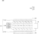
Reference is made to FIGS. 1 and 2 . FIG. 1 is a schematic diagram of an electronic apparatus 100 according to an embodiment of the disclosure. FIG. 2 is a partial view of some components of the electronic apparatus 100 in FIG. 1 . As shown in FIGS. 1 and 2 , the electronic apparatus 100 of the present embodiment is a touch display device as an example and includes a three-dimensional sensing module 110 and a display module 120. The display module 120 is disposed under the three-dimensional sensing module 110.
Specifically, the three-dimensional sensing module 110 includes a touch pressure sensing structure 111 and a flexible cover plate 112. The touch pressure sensing structure 111 includes a first flexible touch electrode layer 111 a 1, a second flexible touch electrode layer 111 a 2, and a light-transmitting force-sensitive composite layer 111 b located between the first flexible touch electrode layer 111 a 1 and the second flexible touch electrode layer 111 a 2. The light-transmitting force-sensitive composite layer 111 b includes a first functional spacer layer 111 b 11, a first light-transmitting electrode layer 111 b 21, a second functional spacer layer 111 b 12, a second light-transmitting electrode layer 111 b 22, and a third functional spacer layer 111 b 13. The first functional spacer layer 111 b 11 is coated on the first flexible touch electrode layer 111 a 1. The first light-transmitting electrode layer 111 b 21 is coated on the first functional spacer layer 111 b 11. The second functional spacer layer 111 b 12 is coated on the first light-transmitting electrode layer 111 b 21. The second light-transmitting electrode layer 111 b 22 is coated on the second functional spacer layer 111 b 12. The third functional spacer layer 111 b 13 is coated on the second light-transmitting electrode layer 111 b 22. Resistivities of the first functional spacer layer 111 b 11, the second functional spacer layer 111 b 12, and the third functional spacer layer 111 b 13 are greater than resistivities of the first light-transmitting electrode layer 111 b 21 and the second light-transmitting electrode layer 111 b 22. The second flexible touch electrode layer 111 a 2 is coated on the third functional spacer layer 111 b 13. The flexible cover plate 112 is disposed on the second flexible touch electrode layer 111 a 2.
In some embodiments, the material of the flexible cover plate 112 includes a flexible polymer material. For example, the flexible polymer material includes Colorless Polyimide (PI), but the present disclosure is not limited in this regard.
As shown in FIG. 1 , the three-dimensional sensing module 110 further includes a controller 113. The controller 113 is electrically connected to the first flexible touch electrode layer 111 a 1 and the second flexible touch electrode layer 111 a 2. As shown in FIG. 2 , both the first flexible touch electrode layer 111 a 1 and the second flexible touch electrode layer 111 a 2 are electrode layers after patterning, and the patterns are only for illustration and not intended to limit the scope of the present disclosure. The principle of the controller 113 to detect the touch position signal via the first flexible touch electrode layer 111 a 1 and the second flexible touch electrode layer 111 a 2 will not be described in detail here, and the related art can be referred to.
In some embodiments, at least one of the first flexible touch electrode layer 111 a 1, the first light-transmitting electrode layer 111 b 21, the second light-transmitting electrode layer 111 b 22, or the second flexible touch electrode layer 111 a 2 can be a silver nanowire electrode layer (SNW; also known as AgNW), a metal grid, or an indium tin oxide (ITO) electrode layer, but the present disclosure is not limited in this regard.
In some embodiments, the light-transmitting force-sensitive composite layer 111 b has an optical transmittance greater than 85% and a haze less than 3%. In order to make the light-transmitting force-sensitive composite layer 111 b meet the aforementioned requirements for optical transmittance and haze, in some embodiments, at least one of the first light-transmitting electrode layer 111 b 21 or the second light-transmitting electrode layer 111 b 22 is a silver nanowire electrode layer.
Reference is made to FIG. 3A. FIG. 3A is a partial enlarged view of a light-transmitting force-sensitive composite layer 111 b in FIG. 1 that is not pressed. As shown in FIG. 3A, each of the first light-transmitting electrode layer 111 b 21 and the second light-transmitting electrode layer 111 b 22 includes a substrate and silver nanowires doped therein. The silver nanowires overlap each other in the substrate to form a conductive network. The substrate refers to a non-nanosilver material formed by a solution including the silver nanowires through processes such as coating, heating, and drying. The silver nanowires are distributed or embedded in the substrate and partially protrude out from the substrate. The substrate can protect the silver nanowires from the external environment, such as to protect against corrosion and abrasion. In some embodiments, the substrate is compressible.
In some embodiments, a wire length of the silver nanowires ranges from about 10 μm to about 300 μm. In some embodiments, a wire diameter (or a wire width) of the silver nanowires is less than about 500 nm. In some embodiments, the silver nanowires can be deformed forms such as other conductive metal nanowires or non-conductive nanowires coated with silver. The use of the silver nanowires to form the silver nanowire electrode layers has the following advantages compared with ITO: low price, simple process, good flexibility, resistance to bending, and etc.
In order to make the light-transmitting force-sensitive composite layer 111 b meet the aforementioned requirements for optical transmittance and haze, in some embodiments, the first functional spacer layer 111 b 11, the second functional spacer layer 111 b 12, and the third functional spacer layer 111 b 13 can be light-transmitting coatings. In some embodiments, as shown in FIG. 3A, at least one of the first functional spacer layer 111 b 11, the second functional spacer layer 111 b 12, or the third functional spacer layer 111 b 13 can be a substrate layer doped with a low-concentration of silver nanowires. Specifically, each of the first functional spacer layer 111 b 11, the second functional spacer layer 111 b 12, and the third functional spacer layer 111 b 13 includes a substrate layer doped with a low-concentration of silver nanowires, so that resistivities of the first functional spacer layer 111 b 11, the second functional spacer layer 111 b 12, and the third functional spacer layer 111 b 13 are greater than resistivities of the first light-transmitting electrode layer 111 b 21 and the second light-transmitting electrode layer 111 b 22, and the first functional spacer layer 111 b 11, the second functional spacer layer 111 b 12, and the third functional spacer layer 111 b 13 have greater optical transmittances. In some embodiments, the substrates of the first functional spacer layer 111 b 11, the second functional spacer layer 111 b 12, and the third functional spacer layer 111 b 13 are identical to the substrates of the first light-transmitting electrode layer 111 b 21 and the second light-transmitting electrode layer 111 b 22, but the present disclosure is not limited in this regard.
In some embodiments, the resistivities of the first flexible touch electrode layer 111 a 1 and the second flexible touch electrode layer 111 a 2 range from 1 Ops (Ohm per Square) to 150 Ops (preferably 60 Ops), but the present disclosure is not limited in this regard. In some embodiments, the resistivities of the first light-transmitting electrode layer 111 b 21 and the second light-transmitting electrode layer 111 b 22 range from 150 Ops to 500 Ops (preferably 300 Ops), but the present disclosure is not limited in this regard. In some embodiments, the resistivity of the second functional spacer layer 111 b 12 ranges from 500 Ops to 1000 Ops (preferably 600 Ops), but the present disclosure is not limited in this regard. In some embodiments, the resistivities of the first functional spacer layer 111 b 11 and the third functional spacer layer 111 b 13 range from 800 Ops to 1200 Ops (preferably 800 Ops), but the present disclosure is not limited in this regard.
In practical applications, the resistivity can be measured to verify whether the concentration of the doped silver nanowires is high (e.g., the first light-transmitting electrode layer 111 b 21 and the second light-transmitting electrode layer 111 b 22) or low (e.g., the first functional spacer layer 111 b 11, the second functional spacer layer 111 b 12, and the third functional spacer layer 111 b 13). In addition, for the first functional spacer layer 111 b 11, the second functional spacer layer 111 b 12, and the third functional spacer layer 111 b 13 that are also doped with low-concentrations of silver nanowires, the difference in resistivity is related to the thickness.
Reference is made to FIG. 3B. FIG. 3B is a partial enlarged view of the light-transmitting force-sensitive composite layer 111 b in FIG. 1 that is pressed. As shown in FIGS. 3A and 3B, since the first light-transmitting electrode layer 111 b 21 and the second light-transmitting electrode layer 111 b 22 are made of silver nanowires, when an external pressing force from the side of the flexible cover plate 112 is transmitted to the light-transmitting force-sensitive composite layer 111 b, the first light-transmitting electrode layer 111 b 21 and the second light-transmitting electrode layer 111 b 22 will be compressed by the force to cause the silver nanowires inside to approach and pass through the first functional spacer layer 111 b 11, the second functional spacer layer 111 b 12, and the third functional spacer layer 111 b 13. When the number of contacting points increases, the overall conductivity of the light-transmitting force-sensitive composite layer 111 b is improved (i.e., the resistivity decreases). For example, as shown in FIG. 3A, when the light-transmitting force-sensitive composite layer 111 b has not been pressed, the silver nanowire L1 in the first light-transmitting electrode layer 111 b 21 and the silver nanowire L2 in the second functional spacer layer 111 b 12 do not contact each other. As shown in FIG. 3B, when the light-transmitting force-sensitive composite layer 111 b is pressed, the silver nanowire L1 in the first light-transmitting electrode layer 111 b 21 will further penetrate into the second functional spacer layer 111 b 12 to contact the silver nanowire L2. Therefore, after detecting the change in the resistivity of the light-transmitting force-sensitive composite layer 111 b through the first flexible touch electrode layer 111 a 1 and the second flexible touch electrode layer 111 a 2, the controller 113 can calculate the value of the external pressing force. For example, if the external pressing force is large, the resistivity of the light-transmitting force-sensitive composite layer 111 b has a greater amount of change; on the contrary, if the external pressing force is small, the resistivity of the light-transmitting force-sensitive composite layer 111 b has a small amount of change. Therefore, the value of the external pressing force can be calculated by the change in resistivity of the light-transmitting force-sensitive composite layer 111 b.
In some embodiments, the controller 113 can simultaneously detect the touch position signal and the pressure sensing signal. In some other embodiments, the controller 113 can sequentially detect the touch position signal and the pressure sensing signal.
In some embodiments, a thickness of the second functional spacer layer 111 b 12 ranges from about 30 nm to about 100 nm (preferably from about 40 nm to about 80 nm).
Under the foregoing configuration, the resistivity between the light-transmitting force-sensitive composite layer 111 b and the first flexible touch electrode layer 111 a 1 and the second flexible touch electrode layer 111 a 2 can be increased. Therefore, when the controller 113 detects the touch position signal, the capacitive sensing signal obtained through the first flexible touch electrode layer 111 a 1 and the second flexible touch electrode layer 111 a 2 is not easily interfered with by the light-transmitting force-sensitive composite layer 111 b and is clearer.
It should be pointed out that in some embodiments, as shown in FIG. 1 , each of the first light-transmitting electrode layer 111 b 21 and the second light-transmitting electrode layer 111 b 22 of the light-transmitting force-sensitive composite layer 111 b is a monolithic structure and can provide a single-finger detection function, but the present disclosure is not limited in this regard. Reference is made to FIG. 4 . FIG. 4 is a schematic diagram of an electronic apparatus 200 according to another embodiment of the disclosure.
As shown in FIG. 4 , the electronic apparatus 200 includes a three-dimensional sensing module 210 and a display module 120. The three-dimensional sensing module 210 includes a touch pressure sensing structure 211 and a flexible cover plate 112. The touch pressure sensing structure 211 includes a first flexible touch electrode layer 111 a 1, a second flexible touch electrode layer 111 a 2, and a light-transmitting force-sensitive composite layer 211 b located between the first flexible touch electrode layer 111 a 1 and the second flexible touch electrode layer 111 a 2. The light-transmitting force-sensitive composite layer 211 b includes a first functional spacer layer 111 b 11, a first light-transmitting electrode layer 211 b 21, a second functional spacer layer 111 b 12, a second light-transmitting electrode layer 211 b 22, and a third functional spacer layer 111 b 13. Compared with the embodiment shown in FIG. 1 , the electronic apparatus 200 of this embodiment is modified with respect to the first light-transmitting electrode layer 211 b 21 and the second light-transmitting electrode layer 211 b 22.
Specifically, each of the first light-transmitting electrode layer 211 b 21 and the second light-transmitting electrode layer 211 b 22 includes a plurality of electrode blocks. The electrode blocks are spaced apart from each other. During manufacturing, the first light-transmitting electrode layer 111 b 21 and the second light-transmitting electrode layer 111 b 22 shown in FIG. 1 can be patterned, so as to obtain the first light-transmitting electrode layer 211 b 21 and the second light-transmitting electrode layer 211 b 22 including pluralities of electrode blocks as illustrated in FIG. 4 , respectively. With the separated electrode blocks, the controller 113 can achieve multi-finger detection.
Reference is made to FIG. 5 . FIG. 5 is a flowchart of a method of manufacturing a three-dimensional sensing module according to an embodiment of the disclosure. As shown in FIG. 5 , a method of manufacturing a three-dimensional sensing module includes steps S101 to S103.
In step S101, a first flexible touch electrode layer is formed.
In step S102, a light-transmitting force-sensitive composite layer is coated on the first flexible touch electrode layer, in which the light-transmitting force-sensitive composite layer includes at least one light-transmitting electrode layer and at least one functional spacer layer, and a resistivity of the light-transmitting electrode layer is smaller than a resistivity of the functional spacer layer.
In step S103, a second flexible touch electrode layer is coated on the light-transmitting force-sensitive composite layer.
In some embodiments, step S102 includes steps S102 a to S102 e.
In step S102 a, a first functional spacer layer is coated on the first flexible touch electrode layer.
In step S102 b, a first light-transmitting electrode layer is coated on the first functional spacer layer.
In step S102 c, a second functional spacer layer is coated on the first light-transmitting electrode layer.
In step S102 d, a second light-transmitting electrode layer is coated on the second functional spacer layer.
In step S102 e, a third functional spacer layer is coated on the second light-transmitting electrode layer.
In some embodiments, the coating processes in the foregoing steps include a spin coating process or a slit die coating, but the present disclosure is not limited in this regard.
In some embodiments, a step of patterning the first light-transmitting electrode layer can be added between step S102 b and step S102 c, and a step of patterning the second light-transmitting electrode layer can be added between step S102 d and step S102 e.
According to the foregoing recitations of the embodiments of the disclosure, it can be seen that in the three-dimensional sensing module of the present disclosure, the touch pressure sensing structure is formed by two flexible touch electrode layers and a light-transmitting force-sensitive composite layer stacked therebetween, so as to provide a two-dimensional touch position signal and a third-dimensional pressure sensing signal at the same time. The three-dimensional sensing module of the present disclosure can be simply completed by only multiple coating processes. Therefore, compared with the conventional complicated method of separately manufacturing the touch module and the display module and then gluing them, the manufacturing process of the three-dimensional sensing module of the present disclosure can completely eliminate the use of glue. As a result, the multi-layer gluing process and the thickness of the glue can be reduced, so that the three-dimensional sensing module of the present disclosure can realize a thin design.
Although the present disclosure has been described in considerable detail with reference to certain embodiments thereof, other embodiments are possible. Therefore, the spirit and scope of the appended claims should not be limited to the description of the embodiments contained herein.
It will be apparent to those skilled in the art that various modifications and variations can be made to the structure of the present disclosure without departing from the scope or spirit of the disclosure. In view of the foregoing, it is intended that the present disclosure cover modifications and variations of this disclosure provided they fall within the scope of the following claims.

Claims (19)

What is claimed is:
1. A three-dimensional sensing module, comprising a touch pressure sensing structure, the touch pressure sensing structure comprising:
a first flexible touch electrode layer;
a first functional spacer layer coated on the first flexible touch electrode layer;
a first light-transmitting electrode layer coated on the first functional spacer layer;
a second functional spacer layer coated on the first light-transmitting electrode layer;
a second light-transmitting electrode layer coated on the second functional spacer layer;
a third functional spacer layer coated on the second light-transmitting electrode layer; and
a second flexible touch electrode layer coated on the third functional spacer layer, wherein:
resistivities of the first functional spacer layer, the second functional spacer layer, and the third functional spacer layer are greater than resistivities of the first light-transmitting electrode layer and the second light-transmitting electrode layer,
resistivities of the first flexible touch electrode layer and the second flexible touch electrode layer range from 1 Ops to 150 Ops,
the resistivities of the first light-transmitting electrode layer and the second light-transmitting electrode layer range from 150 Ops to 500 Ops,
the resistivity of the second functional spacer layer ranges from 500 Ops to 1000 Ops, and
the resistivities of the first functional spacer layer and the third functional spacer layer range from 800 Ops to 1200 Ops.
2. The three-dimensional sensing module of claim 1,
wherein the three-dimensional sensing module further comprises a flexible cover plate disposed on the second flexible touch electrode layer.
3. The three-dimensional sensing module of claim 1, further comprising a controller configured to detect a touch position signal and a pressure sensing signal through the first flexible touch electrode layer and the second flexible touch electrode layer.
4. The three-dimensional sensing module of claim 1, wherein at least one of the first flexible touch electrode layer, the first light-transmitting electrode layer, the second light-transmitting electrode layer, or the second flexible touch electrode layer is a silver nanowire electrode layer.
5. The three-dimensional sensing module of claim 1, wherein thicknesses of the first functional spacer layer and the third functional spacer layer are substantially the same.
6. The three-dimensional sensing module of claim 5, wherein a thickness of the second functional spacer layer is smaller than the thickness of at least one of the first functional spacer layer or the third functional spacer layer.
7. The three-dimensional sensing module of claim 6, wherein the thickness of the second functional spacer layer ranges from 30 nm to 100 nm, and the thicknesses of the first functional spacer layer and the third functional spacer layer range from 400 nm to 1200 nm.
8. The three-dimensional sensing module of claim 1, wherein each of the first light-transmitting electrode layer and the second light-transmitting electrode layer comprises a plurality of electrode blocks spaced apart from each other.
9. The three-dimensional sensing module of claim 1, wherein at least one of the first functional spacer layer, the second functional spacer layer, or the third functional spacer layer is a substrate layer doped with a low-concentration of silver nanowires.
10. An electronic apparatus, comprising:
the three-dimensional sensing module of claim 1; and
a display module disposed under the three-dimensional sensing module.
11. A three-dimensional sensing module, comprising a touch pressure sensing structure, the touch pressure sensing structure comprising:
a first functional spacer layer;
a first light-transmitting electrode layer coated on the first functional spacer layer;
a second functional spacer layer coated on the first light-transmitting electrode layer;
a second light-transmitting electrode layer coated on the second functional spacer layer; and
a third functional spacer layer coated on the second light-transmitting electrode layer, wherein:
resistivities of the first functional spacer layer, the second functional spacer layer, and the third functional spacer layer are greater than resistivities of the first light-transmitting electrode layer and the second light-transmitting electrode layer,
thicknesses of the first functional spacer layer and the third functional spacer layer are substantially the same, and
a thickness of the second functional spacer layer is smaller than the thickness of at least one of the first functional spacer layer or the third functional spacer layer.
12. The three-dimensional sensing module of claim 11, wherein the touch pressure sensing structure further comprises:
a first flexible touch electrode layer, wherein the first functional spacer layer is coated on the first flexible touch electrode layer; and
a second flexible touch electrode layer coated on the third functional spacer layer.
13. The three-dimensional sensing module of claim 12, further comprising a controller configured to detect a touch position signal and a pressure sensing signal through the first flexible touch electrode layer and the second flexible touch electrode layer.
14. The three-dimensional sensing module of claim 12, wherein at least one of the first flexible touch electrode layer, the first light-transmitting electrode layer, the second light-transmitting electrode layer, or the second flexible touch electrode layer is a silver nanowire electrode layer.
15. The three-dimensional sensing module of claim 12, wherein the three-dimensional sensing module further comprises a flexible cover plate disposed on the second flexible touch electrode layer.
16. The three-dimensional sensing module of claim 11, wherein the thickness of the second functional spacer layer ranges from 30 nm to 100 nm, and the thicknesses of the first functional spacer layer and the third functional spacer layer range from 400 nm to 1200 nm.
17. The three-dimensional sensing module of claim 11, wherein each of the first light-transmitting electrode layer and the second light-transmitting electrode layer comprises a plurality of electrode blocks spaced apart from each other.
18. The three-dimensional sensing module of claim 11, wherein at least one of the first functional spacer layer, the second functional spacer layer, or the third functional spacer layer is a substrate layer doped with a low-concentration of silver nanowires.
19. An electronic apparatus, comprising:
the three-dimensional sensing module of claim 11; and
a display module disposed under the three-dimensional sensing module.
US17/011,108 2020-09-03 2020-09-03 Three-dimensional sensing module and method of manufacturing the same and electronic apparatus Active 2040-09-16 US11520429B2 (en)

Priority Applications (1)

Application Number Priority Date Filing Date Title
US17/011,108 US11520429B2 (en) 2020-09-03 2020-09-03 Three-dimensional sensing module and method of manufacturing the same and electronic apparatus

Applications Claiming Priority (1)

Application Number Priority Date Filing Date Title
US17/011,108 US11520429B2 (en) 2020-09-03 2020-09-03 Three-dimensional sensing module and method of manufacturing the same and electronic apparatus

Publications (2)

Publication Number Publication Date
US20220066608A1 US20220066608A1 (en) 2022-03-03
US11520429B2 true US11520429B2 (en) 2022-12-06

Family

ID=80356842

Family Applications (1)

Application Number Title Priority Date Filing Date
US17/011,108 Active 2040-09-16 US11520429B2 (en) 2020-09-03 2020-09-03 Three-dimensional sensing module and method of manufacturing the same and electronic apparatus

Country Status (1)

Country Link
US (1) US11520429B2 (en)

Families Citing this family (1)

* Cited by examiner, † Cited by third party
Publication number Priority date Publication date Assignee Title
TW202424442A (en) * 2022-11-30 2024-06-16 致伸科技股份有限公司 Force-sensing key module and force-sensing switch structure thereof

Citations (9)

* Cited by examiner, † Cited by third party
Publication number Priority date Publication date Assignee Title
KR20110120121A (en) 2010-04-28 2011-11-03 강석주 Capacitive touch panel
US20140307186A1 (en) 2011-10-27 2014-10-16 Lg Innotek Co., Ltd. Touch panel
WO2015025491A1 (en) * 2013-08-23 2015-02-26 Sony Corporation Display unit
US20170031491A1 (en) 2015-07-29 2017-02-02 The Board Of Trustees Of The Leland Stanford Junior University Methods and apparatus concerning sensitive force sensors
TW201905668A (en) 2017-06-15 2019-02-01 禾瑞亞科技股份有限公司 Pressure sensing touch control device for accurately calculating the pressure exerted by an external object on a pressure sensing touch panel and also enhancing the application and effect of touch control through pressure sensing
KR20190052403A (en) 2017-11-08 2019-05-16 한국기술교육대학교 산학협력단 Pressure sensor having silver nano-wire and manufacturing method thereof
US20190196633A1 (en) * 2017-12-11 2019-06-27 Tpk Touch Solutions (Xiamen) Inc. Touch sensor, touch panel and method for manufacturing the same
CN110703935A (en) 2018-07-10 2020-01-17 Smk株式会社 touch panel
TWM605319U (en) 2020-07-28 2020-12-11 大陸商宸美(廈門)光電有限公司 Three-dimensional sensing module and electronic apparatus

Patent Citations (9)

* Cited by examiner, † Cited by third party
Publication number Priority date Publication date Assignee Title
KR20110120121A (en) 2010-04-28 2011-11-03 강석주 Capacitive touch panel
US20140307186A1 (en) 2011-10-27 2014-10-16 Lg Innotek Co., Ltd. Touch panel
WO2015025491A1 (en) * 2013-08-23 2015-02-26 Sony Corporation Display unit
US20170031491A1 (en) 2015-07-29 2017-02-02 The Board Of Trustees Of The Leland Stanford Junior University Methods and apparatus concerning sensitive force sensors
TW201905668A (en) 2017-06-15 2019-02-01 禾瑞亞科技股份有限公司 Pressure sensing touch control device for accurately calculating the pressure exerted by an external object on a pressure sensing touch panel and also enhancing the application and effect of touch control through pressure sensing
KR20190052403A (en) 2017-11-08 2019-05-16 한국기술교육대학교 산학협력단 Pressure sensor having silver nano-wire and manufacturing method thereof
US20190196633A1 (en) * 2017-12-11 2019-06-27 Tpk Touch Solutions (Xiamen) Inc. Touch sensor, touch panel and method for manufacturing the same
CN110703935A (en) 2018-07-10 2020-01-17 Smk株式会社 touch panel
TWM605319U (en) 2020-07-28 2020-12-11 大陸商宸美(廈門)光電有限公司 Three-dimensional sensing module and electronic apparatus

Also Published As

Publication number Publication date
US20220066608A1 (en) 2022-03-03

Similar Documents

Publication Publication Date Title
TWI557605B (en) Positional touch sensor with force measurement
TWI609305B (en) Pressure sensing input device
KR20140129135A (en) Touch sensor electrode with patterned electrically isolated regions
US11068100B1 (en) Electronic apparatus
US11520429B2 (en) Three-dimensional sensing module and method of manufacturing the same and electronic apparatus
US11216143B1 (en) Force sensing module and method of manufacturing the same and electronic device
TWM605319U (en) Three-dimensional sensing module and electronic apparatus
CN212433743U (en) 3D sensing module and electronic device
KR102404067B1 (en) Three-dimensional sensing module and method of manufacturing the same and electronic apparatus
US11269435B1 (en) Three-dimensional sensing panel and method of manufacturing the same and electronic apparatus
CN212749793U (en) Electronic device
TWI746093B (en) Three-dimensional sensing module and method of manufacturing the same and electronic apparatus
CN212541302U (en) Three-dimensional sensing panel and electronic device
TWI749669B (en) Three-dimensional sensing panel and method of manufacturing the same and electronic apparatus
JP2022022046A (en) Three-dimensional detection panel and method for producing the same, and electronic apparatus
KR20140046943A (en) Touch panel and method for manufacturing the same

Legal Events

Date Code Title Description
FEPP Fee payment procedure

Free format text: ENTITY STATUS SET TO UNDISCOUNTED (ORIGINAL EVENT CODE: BIG.); ENTITY STATUS OF PATENT OWNER: LARGE ENTITY

AS Assignment

Owner name: TPK ADVANCED SOLUTIONS INC., CHINA

Free format text: ASSIGNMENT OF ASSIGNORS INTEREST;ASSIGNORS:LEE, LIEN HSIN;WANG, REN HUNG;YE, CAI JIN;AND OTHERS;SIGNING DATES FROM 20200819 TO 20200831;REEL/FRAME:053705/0326

STPP Information on status: patent application and granting procedure in general

Free format text: NON FINAL ACTION MAILED

STPP Information on status: patent application and granting procedure in general

Free format text: RESPONSE TO NON-FINAL OFFICE ACTION ENTERED AND FORWARDED TO EXAMINER

STPP Information on status: patent application and granting procedure in general

Free format text: NOTICE OF ALLOWANCE MAILED -- APPLICATION RECEIVED IN OFFICE OF PUBLICATIONS

STPP Information on status: patent application and granting procedure in general

Free format text: PUBLICATIONS -- ISSUE FEE PAYMENT VERIFIED

STCF Information on status: patent grant

Free format text: PATENTED CASE