US11496703B2 - High conversion gain and high fill-factor image sensors with pump-gate and vertical charge storage well for global-shutter and high-speed applications - Google Patents
High conversion gain and high fill-factor image sensors with pump-gate and vertical charge storage well for global-shutter and high-speed applications Download PDFInfo
- Publication number
- US11496703B2 US11496703B2 US16/938,939 US202016938939A US11496703B2 US 11496703 B2 US11496703 B2 US 11496703B2 US 202016938939 A US202016938939 A US 202016938939A US 11496703 B2 US11496703 B2 US 11496703B2
- Authority
- US
- United States
- Prior art keywords
- storage
- transfer
- gate
- node
- region
- Prior art date
- Legal status (The legal status is an assumption and is not a legal conclusion. Google has not performed a legal analysis and makes no representation as to the accuracy of the status listed.)
- Active, expires
Links
Images




Classifications
-
- H—ELECTRICITY
- H10—SEMICONDUCTOR DEVICES; ELECTRIC SOLID-STATE DEVICES NOT OTHERWISE PROVIDED FOR
- H10F—INORGANIC SEMICONDUCTOR DEVICES SENSITIVE TO INFRARED RADIATION, LIGHT, ELECTROMAGNETIC RADIATION OF SHORTER WAVELENGTH OR CORPUSCULAR RADIATION
- H10F39/00—Integrated devices, or assemblies of multiple devices, comprising at least one element covered by group H10F30/00, e.g. radiation detectors comprising photodiode arrays
- H10F39/80—Constructional details of image sensors
- H10F39/803—Pixels having integrated switching, control, storage or amplification elements
- H10F39/8037—Pixels having integrated switching, control, storage or amplification elements the integrated elements comprising a transistor
-
- H04N5/37452—
-
- H—ELECTRICITY
- H04—ELECTRIC COMMUNICATION TECHNIQUE
- H04N—PICTORIAL COMMUNICATION, e.g. TELEVISION
- H04N25/00—Circuitry of solid-state image sensors [SSIS]; Control thereof
- H04N25/70—SSIS architectures; Circuits associated therewith
- H04N25/76—Addressed sensors, e.g. MOS or CMOS sensors
- H04N25/77—Pixel circuitry, e.g. memories, A/D converters, pixel amplifiers, shared circuits or shared components
- H04N25/771—Pixel circuitry, e.g. memories, A/D converters, pixel amplifiers, shared circuits or shared components comprising storage means other than floating diffusion
-
- H01L27/1461—
-
- H—ELECTRICITY
- H04—ELECTRIC COMMUNICATION TECHNIQUE
- H04N—PICTORIAL COMMUNICATION, e.g. TELEVISION
- H04N25/00—Circuitry of solid-state image sensors [SSIS]; Control thereof
- H04N25/70—SSIS architectures; Circuits associated therewith
- H04N25/76—Addressed sensors, e.g. MOS or CMOS sensors
- H04N25/78—Readout circuits for addressed sensors, e.g. output amplifiers or A/D converters
-
- H04N5/378—
-
- H—ELECTRICITY
- H10—SEMICONDUCTOR DEVICES; ELECTRIC SOLID-STATE DEVICES NOT OTHERWISE PROVIDED FOR
- H10F—INORGANIC SEMICONDUCTOR DEVICES SENSITIVE TO INFRARED RADIATION, LIGHT, ELECTROMAGNETIC RADIATION OF SHORTER WAVELENGTH OR CORPUSCULAR RADIATION
- H10F39/00—Integrated devices, or assemblies of multiple devices, comprising at least one element covered by group H10F30/00, e.g. radiation detectors comprising photodiode arrays
- H10F39/80—Constructional details of image sensors
- H10F39/802—Geometry or disposition of elements in pixels, e.g. address-lines or gate electrodes
-
- H—ELECTRICITY
- H10—SEMICONDUCTOR DEVICES; ELECTRIC SOLID-STATE DEVICES NOT OTHERWISE PROVIDED FOR
- H10F—INORGANIC SEMICONDUCTOR DEVICES SENSITIVE TO INFRARED RADIATION, LIGHT, ELECTROMAGNETIC RADIATION OF SHORTER WAVELENGTH OR CORPUSCULAR RADIATION
- H10F39/00—Integrated devices, or assemblies of multiple devices, comprising at least one element covered by group H10F30/00, e.g. radiation detectors comprising photodiode arrays
- H10F39/80—Constructional details of image sensors
- H10F39/803—Pixels having integrated switching, control, storage or amplification elements
- H10F39/8033—Photosensitive area
-
- H—ELECTRICITY
- H10—SEMICONDUCTOR DEVICES; ELECTRIC SOLID-STATE DEVICES NOT OTHERWISE PROVIDED FOR
- H10F—INORGANIC SEMICONDUCTOR DEVICES SENSITIVE TO INFRARED RADIATION, LIGHT, ELECTROMAGNETIC RADIATION OF SHORTER WAVELENGTH OR CORPUSCULAR RADIATION
- H10F39/00—Integrated devices, or assemblies of multiple devices, comprising at least one element covered by group H10F30/00, e.g. radiation detectors comprising photodiode arrays
- H10F39/80—Constructional details of image sensors
- H10F39/813—Electronic components shared by multiple pixels, e.g. one amplifier shared by two pixels
-
- H—ELECTRICITY
- H10—SEMICONDUCTOR DEVICES; ELECTRIC SOLID-STATE DEVICES NOT OTHERWISE PROVIDED FOR
- H10F—INORGANIC SEMICONDUCTOR DEVICES SENSITIVE TO INFRARED RADIATION, LIGHT, ELECTROMAGNETIC RADIATION OF SHORTER WAVELENGTH OR CORPUSCULAR RADIATION
- H10F39/00—Integrated devices, or assemblies of multiple devices, comprising at least one element covered by group H10F30/00, e.g. radiation detectors comprising photodiode arrays
- H10F39/10—Integrated devices
- H10F39/12—Image sensors
- H10F39/199—Back-illuminated image sensors
Definitions
- Modern image sensors typically include a number of light-sensitive picture elements (“pixels”) arranged in a two-dimensional array (e.g., a rectangular array) coupled to circuitry for reading and controlling the pixel array. After each pixel has acquired its image data (e.g., by collecting charge during an exposure period), the image data is read out by the readout circuitry, which may include amplification circuitry, analog-to-digital conversion circuitry, etc.
- the readout circuitry which may include amplification circuitry, analog-to-digital conversion circuitry, etc.
- High-speed image sensors for use in time-resolved imaging and global shutter applications are widely sought after. Such sensors can benefit many applications, such as scientific imaging, time-of-flight estimation, motion traction, augmented reality, etc.
- applications such as scientific imaging, time-of-flight estimation, motion traction, augmented reality, etc.
- FIG. 1 is an illustration of an exemplary global-shutter image sensor in accordance with some embodiments.
- FIG. 2A illustrates a layout for an exemplary detector in accordance with some embodiments.
- FIG. 2B is an exemplary cross-sectional view of the exemplary detector of FIG. 2A in accordance with some embodiments.
- FIG. 2C illustrates a cross-sectional view of an exemplary detector of FIG. 2A shown with exemplary control and readout circuitry in accordance with some embodiments.
- FIG. 2D illustrates the lateral area and lateral perimeter of the storage well as compared to the lateral area and lateral perimeter of the storage node in accordance with some embodiments.
- FIG. 3 is an operating timing and charge transfer diagram to illustrate operation of the exemplary detector illustrated in FIGS. 2A, 2B, 2C, and 2D .
- FIGS. 4A, 4B, and 4C illustrate charge transfer of a horizontal pump gate structure in accordance with some embodiments.
- FIG. 5A illustrates a layout of an exemplary detector in accordance with some embodiments.
- FIG. 5B illustrates a layout of another exemplary detector in accordance with some embodiments.
- FIG. 5C is a cross-sectional view applicable to both of the exemplary detectors illustrated in FIGS. 5A and 5B .
- FIG. 6A illustrates a cross-sectional view of an exemplary detector with exemplary control and readout circuitry that includes a punch-through reset diode in accordance with some embodiments.
- FIG. 6B illustrates a cross-sectional view of an exemplary detector with exemplary control and readout circuitry that includes a JFET source-follower in accordance with some embodiments.
- FIG. 6C illustrates a cross-sectional view of an exemplary detector with exemplary control and readout circuitry that includes a JFET source-follower and punch-through reset diode in accordance with some embodiments.
- FIG. 7A illustrates an exemplary layout for an exemplary image sensor with a non-shared readout in accordance with some embodiments.
- FIG. 7B illustrates an exemplary layout for an exemplary image sensor with two-way shared control and readout circuitry in accordance with some embodiments.
- FIG. 7C illustrates an exemplary layout for an exemplary image sensor with four-way shared control and readout circuitry in accordance with some embodiments.
- FIG. 7D illustrates another exemplary layout for an exemplary image sensor with four-way shared control and readout circuitry in accordance with some embodiments.
- FIG. 8 is an illustration of an exemplary multi-tap time-resolved sensor without in-pixel storage nodes in accordance with some embodiments.
- FIG. 9A illustrates an exemplary layout of an exemplary two-tap detector in accordance with some embodiments.
- FIG. 9B illustrates a cross-sectional view of the exemplary detector of FIG. 9A with exemplary control and readout circuitry in accordance with some embodiments.
- FIG. 9C illustrates a cross-sectional view of the exemplary detector of FIG. 9A in accordance with some embodiments.
- FIG. 9D illustrates an exemplary layout for an exemplary 4-tap detector in accordance with some embodiments.
- FIG. 10 is an exemplary control signal timing diagram for a multi-tap system in accordance with some embodiments.
- FIGS. 11A, 11B, 11C, 11D, 11E, and 11F illustrate how charge can be transferred by the exemplary detector illustrated in FIGS. 9A-9C in accordance with some embodiments.
- FIG. 12A illustrates an exemplary layout for an exemplary multi-tap detector with a punch-through reset drain in accordance with some embodiments.
- FIGS. 12B and 12C illustrate cross-sectional views of the exemplary detector of FIG. 12A in accordance with some embodiments.
- FIG. 13 is an illustration of an exemplary multi-tap time-resolved sensor with in-pixel storage nodes in accordance with some embodiments.
- FIG. 14A illustrates an exemplary layout for an exemplary multi-tap time-resolved pump-gate detector with pinned storage nodes and shared control and readout circuitry in accordance with some embodiments.
- FIG. 14B illustrates a cross-sectional view of the exemplary detector of FIG. 14A in accordance with some embodiments.
- FIG. 14C illustrates a cross-sectional view of the exemplary detector of FIG. 14A with exemplary control and readout circuitry in accordance with some embodiments.
- FIGS. 15A, 15B, 15C, and 15D illustrate how charge can be transferred by the exemplary detector illustrated in FIGS. 14A-14C in accordance with some embodiments.
- pixel and “detector” are used interchangeably herein.
- rolling shutter Two modes used in imaging devices and systems for reading image data from a pixel array are known as “rolling shutter” and “global shutter.”
- An imaging system or device operating in the rolling shutter mode exposes and reads out adjacent rows of a pixel array at different times, with each row read after its exposure has been completed. Consequently, the exposure of each row is slightly offset in time from its neighbors.
- the row at one end of the pixel array e.g., the top row of the array
- the bottom row of the array e.g., the bottom row of the array. The time difference depends on the number of rows and the offset in time between adjacent rows.
- rolling shutter mode As a result of the time difference, spatial distortion can result from rolling shutter mode.
- the distortion increases, for example, when objects are moving at a rate that is faster than the readout rate.
- a potential benefit of rolling shutter mode is that it may provide a larger fill-factor, higher quantum efficiency, larger full-well capacity and dynamic range than global shutter mode.
- each pixel transfers its signal charge to a readout node.
- One way to implement global shutter pixels is by using a photodiode and a memory element within each pixel of the image sensor array.
- the photodiode collects signal charge during an exposure.
- the memory element referred to herein as an in-pixel storage node (abbreviated as “SN”), temporarily stores photo-generated charges and allows each pixel in the image sensor array to be exposed at the same time. At the end of the exposure time, photo-generated charge carriers are transferred from photodiodes to the in-pixel memory nodes.
- CMOS complementary metal-oxide semiconductor
- FSI frontside-illuminated
- BI backside-illuminated
- An FSI CMOS imaging pixel may include a substrate upon which pixel circuitry is disposed and over which one or more metal layers are patterned to create an optical passage through which light incident on the frontside of imaging pixel can reach a photosensitive (or photodiode) region.
- the frontside may also include a color filter layer to implement a color sensor and a microlens to focus the light onto photodiode region.
- FSI image sensors One issue with FSI image sensors is that, as described above, the one or more metal layers are situated between the photosensitive region of the pixel and the lens. Therefore, they can prevent some of the light from reaching the photo-sensitive region of the pixel, which degrades image quality, especially in low-light conditions. Nevertheless, global shutter pixels are often implemented as FSI image sensors because the metal layers (e.g., frontside shielding metals or reflective coatings) can prevent some or all incident radiation from striking the in-pixel storage node.
- the metal layers e.g., frontside shielding metals or reflective coatings
- the one or more metal layers can mitigate degradation of global shutter efficiency caused by the generation of parasitic electron-hole pairs within the in-pixel storage node (e.g., by preventing the parasitic electron-hole pairs from contaminating charges stored in the pixel-level storage node during an exposure).
- a BSI CMOS imaging pixel may also include a substrate with pixel circuitry, one or more metal layers, a color filter, and a microlens, but some of these components are arranged differently than in FSI pixels.
- the color filter and microlens are on the backside of the pixel, whereas the one or more metal layers remain on the frontside.
- BSI image sensors detect light that is incident upon the backside of the sensor substrate. Incident light can then reach the photosensitive region of the pixel free of interference from the one or more metal layers on the frontside.
- the pixels in a BSI image sensor can capture more light than the pixels in a FSI sensor and thereby offer better quantum efficiency (and better low-light performance) than FSI image sensors because they do not have metal interconnect layers within an optical path of a photodiode (the photo-sensitive region of the pixel).
- BSI image sensors do not have overlying metal interconnect layers to shield pixel-level memory nodes from incident radiation, they can be at a disadvantage relative to FSI image sensors with respect to global shutter efficiency.
- the shielding to protect the in-pixel memory node becomes more complicated because the metals or reflective coatings on the backside cannot block the incident light sufficiently due to the diffraction of the light and the diffusion of the signal charge through the silicon bulk.
- backside metal cannot completely prevent the diffracted light from going into the storage node, nor can it prevent the electrons generated in the substrate from being diffused to the storage node. Both effects are due to a long distance and optical path between the shielding and the storage node.
- Some sensors use vertical reflectors formed with deep trench isolation (DTI) structures on the backside to shield the storage node from light with larger chief angles.
- DTI deep trench isolation
- One way to improve the low- or sparse-light performance of an image sensor is to reduce the input-referred noise floor (e.g., read noise) of the sensor. Reducing the read noise also helps to improve the dynamic range of the sensor, which can be important for certain applications (e.g., high dynamic range imaging, automotive, computer vision, etc.).
- One way to reduce the read noise is to design a detector with high conversion gain.
- U.S. Patent Pub. No. 2015/0301267 describes an image sensor with pump-gate detectors to purportedly improve the conversion gain and, thus, low-light performance.
- a drawback of this architecture is that it is limited to application within a rolling shutter image sensor.
- Some sensor embodiments use a pump gate structure and a vertical charge storage well.
- the disclosed sensors are suitable for use in high-speed global-shutter applications.
- an image sensor apparatus comprises a frontside surface, a backside surface, a storage region, a storage well, and a doping region situated between the storage region and the storage well.
- the storage region may be, for example, a storage node or a floating diffusion node.
- the storage region is situated closer to the frontside surface than to the backside surface, and the storage well is situated between the backside surface and the storage region.
- a lateral area of the storage well is greater than or equal to a lateral area of the storage region, and no portion of a lateral perimeter of the storage region extends outside of a lateral perimeter of the storage well.
- a pinning layer (e.g., a heavily-doped pinning layer) is disposed between the storage region and the frontside surface, the pinning layer being situated adjacent to the storage region.
- the image sensor apparatus also includes a transfer gate formed on the frontside surface.
- the transfer gate is configured to cause charge to transfer from the storage well to the storage region in response to a bias applied to the transfer gate.
- the transfer gate may be situated over at least a portion of the storage well.
- the transfer gate in a plan view of the image sensor apparatus (e.g., from the frontside), the transfer gate extends laterally around at least a portion of the storage region, which may be, in such embodiments, a storage node.
- the storage well comprises a shallow region and a deep region, the deep region being situated between the backside surface and the shallow region.
- a doping of the shallow region is heavier than a doping of the deep region.
- a lateral dimension of the shallow region in a first direction is smaller than a corresponding lateral dimension of the deep region in the first direction.
- the storage region is a storage node
- the image sensor apparatus also includes a floating diffusion node situated between the frontside surface and the backside surface (e.g., closer to the frontside surface than to the backside surface).
- the floating diffusion node may be coupled to circuitry (e.g., for controlling and/or reading the image sensor apparatus and/or the floating diffusion node).
- the circuitry comprises at least one of a MOSFET transistor, a punch-through diode, or a JFET transistor.
- the image sensor apparatus also includes a pump gate structure disposed between the storage node and the floating diffusion node.
- the pump gate structure is configured to cause charge to transfer from the storage node to the floating diffusion node in response to a bias applied to a signal gate coupled to the pump gate structure.
- the pump gate structure comprises a plurality of doping regions (e.g., a virtual barrier region, a p-type barrier region, and a p-type well region situated between the virtual barrier region and the p-type barrier region).
- the p-type barrier region is adjacent to the storage node
- the virtual barrier region is adjacent to the floating diffusion node.
- the image sensor apparatus also includes a signal gate formed on the frontside surface.
- a signal gate formed on the frontside surface.
- Some such embodiments also include a pump gate structure that is horizontal and is situated, at least in part, under the signal gate.
- the image sensor apparatus in addition to a storage node, a floating diffusion node, a pump gate structure, and a signal gate, the image sensor apparatus also includes a transfer gate formed on the frontside surface, wherein the transfer gate is configured to cause charge to transfer from the storage well to the storage node in response to a bias applied to the transfer gate.
- a method of using the image sensor apparatus comprises biasing the transfer gate at a first time, biasing the signal gate at a second time, the second time being after the first time, and reading the floating diffusion node after biasing the signal gate at the second time.
- the method also comprises resetting the floating diffusion node before biasing (e.g., pulsing) the transfer gate at the first time.
- reading the floating diffusion node comprises performing correlated double sampling.
- the storage region is a first storage node and the storage well is a first storage well
- the image sensor apparatus further comprises a second storage node situated closer to the frontside surface than to the backside surface, a second storage well situated between the backside surface and the second storage node, wherein a lateral area of the second storage well is greater than or equal to a lateral area of the second storage node, and no portion of the lateral perimeter of the second storage node extends outside of the lateral perimeter of the second storage well.
- the image sensor apparatus also includes a floating diffusion node disposed between the first and second storage nodes, circuitry coupled to the floating diffusion node, a first transfer gate formed on the frontside surface and configured to cause a first charge to transfer from the first storage well to the first storage node in response to a voltage applied to the first transfer gate, a first signal gate formed on the frontside surface and configured to cause the first charge to transfer from the first storage node to the floating diffusion node in response to a voltage applied to the first signal gate, a second transfer gate formed on the frontside surface and configured to cause a second charge to transfer from the second storage well to the second storage node in response to a voltage applied to the second transfer gate, and a second signal gate formed on the frontside surface and configured to cause the second charge to transfer from the second storage node to the floating diffusion node in response to a voltage applied to the second signal gate.
- the image sensor apparatus further comprises a first pump gate structure disposed between the first storage node and the floating diffusion node, wherein the first pump gate structure is configured to direct the first charge from the first storage node to the floating diffusion node in response to the voltage applied to the first signal gate, the first signal gate being coupled to the first pump gate structure, and a second pump gate structure disposed between the second storage node and the floating diffusion node, wherein the second pump gate structure is configured to direct the second charge from the second storage node to the floating diffusion node in response to the voltage applied to the second signal gate, the second signal gate being coupled to the second pump gate structure.
- the floating diffusion node is a first floating diffusion node
- the image sensor apparatus further comprises a third storage node situated closer to the frontside surface than to the backside surface, a third storage well situated between the backside surface and the third storage node, a fourth storage node, the fourth storage node being situated closer to the frontside surface than to the backside surface, a fourth storage well situated between the backside surface and the fourth storage node, a second floating diffusion node disposed between the third and fourth storage nodes and coupled to the first floating diffusion node, a third transfer gate formed on the frontside surface and configured to cause a third charge to transfer from the third storage well to the third storage node in response to a voltage applied to the third transfer gate, a third signal gate formed on the frontside surface and configured to cause the third charge to transfer from the third storage node to the second floating diffusion node in response to a voltage applied to the third signal gate, a fourth transfer gate formed on the frontside surface and configured to cause a fourth charge to transfer from the fourth storage well to the
- the image sensor apparatus also includes a third storage node situated closer to the frontside surface than to the backside surface, a third storage well situated between the backside surface and the third storage node, a fourth storage node situated closer to the frontside surface than to the backside surface, a fourth storage well situated between the backside surface and the fourth storage node, a third transfer gate formed on the frontside surface and configured to cause a third charge to transfer from the third storage well to the third storage node in response to a voltage applied to the third transfer gate, a third signal gate formed on the frontside surface configured to cause the third charge to transfer from the third storage node to the floating diffusion node in response to a voltage applied to the third signal gate, a fourth transfer gate formed on the frontside surface configured to cause a fourth charge to transfer from the fourth storage well to the fourth storage node in response to a voltage applied to the fourth transfer gate, and a fourth signal gate formed on the frontside surface configured to cause the fourth charge to transfer from the fourth storage node to the floating diffusion node in response to a voltage applied
- the storage region comprises a floating diffusion node.
- the image sensor apparatus further comprises a first storage node, a second storage node, a first horizontal pump gate structure situated between and adjacent to the first storage node and a first side of the floating diffusion node, and a second horizontal pump gate structure situated between and adjacent to the second storage node and a second side of the floating diffusion node.
- each of the first and second horizontal pump gate structures is a multi-layer structure comprising a p-type barrier region, a virtual barrier region, and a p-type well region sandwiched between the p-type barrier region and the virtual barrier region.
- each of the virtual barrier regions is adjacent to the floating diffusion node.
- the image sensor has a floating diffusion node, first and second storage nodes, and first and second horizontal pump gate structures situated between, respectively, the first and second storage nodes and the floating diffusion node
- the image sensor further comprises first and second signal gates and first and second transfer gates formed on the frontside surface.
- the first signal gate is configured to cause first signal charge to transfer from the storage well to the first storage node in response to a first bias applied to the first signal gate
- the second signal gate is configured to cause second signal charge to transfer from the storage well to the second storage node in response to a second bias applied to the second signal gate.
- the first transfer gate is situated above the first pump gate structure and is configured to cause the first signal charge to transfer from the first storage node, through the first pump gate structure, and to the floating diffusion node in response to a third bias applied to the first transfer gate
- the second transfer gate is situated above the second pump gate structure and is configured to cause the second signal charge to transfer from the second storage node, through the second pump gate structure, and to the floating diffusion node in response to a fourth bias applied to the second transfer gate.
- the image sensor apparatus further comprises circuitry (e.g., at least one transistor or diode) coupled to the floating diffusion node.
- the image sensor apparatus further comprises a drain region and a transfer drain gate formed on the frontside surface, wherein the transfer drain gate is configured to cause excess charge to transfer from the storage well to the drain region in response to a bias applied to the transfer drain gate.
- an image sensor with a frontside surface and a backside surface includes a storage well situated between the backside surface and the frontside surface, a pump gate structure situated between the storage well and the frontside surface, a first doping region of the pump gate structure being adjacent to the storage well, a first floating diffusion node situated adjacent to a first side of the pump gate structure, a second floating diffusion node situated adjacent to a second side of the pump gate structure, a first transfer gate configured to direct charge from the storage well to the first floating diffusion node in response to a bias applied to the first transfer gate, and a second transfer gate configured to direct the charge from the storage well to the second floating diffusion node in response to a bias applied to the second transfer gate.
- the storage well comprises a shallow region and a deep region, the deep region being situated between the backside surface and the shallow region.
- a doping of the shallow region is heavier than a doping of the deep region.
- the image sensor also includes circuitry coupled to the first and second floating diffusion nodes.
- the circuitry comprises at least one of a MOSFET transistor, a punch-through diode, or a JFET transistor.
- the pump gate structure comprises a plurality of doping regions.
- the pump gate structure comprises a p-type barrier adjacent to the storage well and a multi-layer structure situated (a) between the p-type barrier and the frontside surface and (b) between the first and second floating diffusion nodes.
- the multi-layer structure comprises a first virtual barrier region, a first p-type well region, a p-type region, a second p-type well region, and a second virtual barrier region, wherein the first and second p-type well regions are situated between the first and second virtual barrier regions, and the p-type region is situated between the first and second p-type well regions.
- a doping of the p-type region is higher than a doping of the first p-type well region and a doping of the second p-type well region.
- the first virtual barrier region is adjacent to the first floating diffusion node, and the second virtual barrier region is adjacent to the second floating diffusion node.
- the image sensor also includes a drain region and a transfer drain gate formed on the frontside surface, and the transfer drain gate is configured to cause charge to transfer from the storage well to the drain region in response to a bias applied to the transfer drain gate.
- the image sensor also includes a punch-through reset drain configured to cause charge to transfer from the storage well in response to a bias exceeding a threshold.
- a backside illumination (BSI) image sensor device comprises a frontside surface, a backside surface, a floating diffusion node, a storage well situated between the backside surface and the floating diffusion node, a first storage node, a second storage node, a first horizontal pump gate structure situated between and adjacent to the first storage node and a first side of the floating diffusion node, and a second horizontal pump gate structure situated between and adjacent to the second storage node and a second side of the floating diffusion node.
- each of the first and second horizontal pump gate structures is a multi-layer structure comprising a p-type barrier region, a virtual barrier region, and a p-type well region sandwiched between the p-type barrier region and the virtual barrier region.
- each of the virtual barrier regions is adjacent to the floating diffusion node.
- the BSI image sensor device also comprises a first signal gate formed on the frontside surface, a second signal gate formed on the frontside surface, a first transfer gate formed on the frontside surface above the first pump gate structure, and a second transfer gate formed on the frontside surface above the second pump gate structure.
- the first signal gate is configured to cause first signal charge to transfer from the storage well to the first storage node in response to a first bias applied to the first signal gate
- the second signal gate is configured to cause second signal charge to transfer from the storage well to the first storage node in response to a second bias applied to the second signal gate
- the first transfer gate is configured to cause the first signal charge to transfer from the first storage node, through the first pump gate structure, and to the floating diffusion node in response to a third bias applied to the first transfer gate
- the second transfer gate is configured to cause the second signal charge to transfer from the second storage node, through the second pump gate structure, and to the floating diffusion node in response to a fourth bias applied to the second transfer gate.
- the BSI image sensor device also includes circuitry coupled to the floating diffusion node.
- the circuitry comprises at least one transistor or diode.
- the BSI image sensor device also includes a drain region and a transfer drain gate formed on the frontside surface, wherein the transfer drain gate is configured to cause excess charge to transfer from the storage well to the drain region in response to a bias applied to the transfer drain gate.
- first and second features are formed in direct contact
- additional features may be formed between the first and second features, such that the first and second features may not be in direct contact
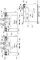
- FIG. 1 is an illustration of an exemplary global-shutter image sensor apparatus 10 A in accordance with some embodiments.
- the exemplary global-shutter image sensor apparatus 10 A includes an array of detectors (also referred to as pixels or sensors), eight of which are labeled in FIG. 1 as 50 A, 50 B, 50 C, 50 D, 50 E, 50 F, 50 G, and 50 Z.
- the array of detectors can be of any suitable size. That the last detector in the first row is labeled as 50 Z is for convenience and not to imply that there are exactly 26 detectors in each row of the array.
- the global-shutter image sensor apparatus 10 A may have any number of detectors 50 A, 50 B, etc. and, accordingly, any number of rows and any number of columns.
- the array can be of any size or shape.
- FIGS. 2A, 2B, and 2C illustrate portions of an exemplary backside-illuminated detector 100 A that may be included in the exemplary global-shutter image sensor apparatus 10 A (e.g., as the detectors 50 A, 50 B, etc.) in accordance with some embodiments.
- FIG. 2A is a plan view (from the frontside surface 195 ) of an exemplary layout for the exemplary detector 100 A
- FIGS. 2B and 2C are cross-sectional views of the exemplary detector 100 A at the locations indicated in FIG. 2A .
- FIGS. 2A-2C may not illustrate all of the elements that may be necessary or desirable to use the pixel or sensor.
- the figures do not illustrate any filters or lenses that may be attached or coupled to the backside surface 190 .
- the plan view of the detector 100 A is in an x-y plane
- the cross-sectional views of FIGS. 2B and 2C are in, respectively, y-z and x-z planes.
- the dimensions of elements of the exemplary detector 100 A in an x-y plane are referred to herein as lateral dimensions.
- a lateral dimension may be in any arbitrary direction in the x-y plane.
- the lateral area of an element is defined as the maximum area occupied by that element in an x-y plane over all possible values of z.
- the lateral perimeter of an element is defined as the element's perimeter in an x-y plane at the value of z corresponding to the lateral area.
- the lateral perimeter of an element is the outline of the lateral area of that element at some position in an x-y plane.
- the lateral perimeter is a shape (e.g., rectangular, square, etc.) at a position in the x-y plane.
- the detector 100 A is formed on/in a substrate 170 , and it has a backside surface 190 and a frontside surface 195 .
- the frontside surface 195 includes a layer of protective material 160 , which may be, for example, an oxide.
- the detector 100 A includes a pinned photodiode, shown as a pinned storage well (SW) 140 , in which signal charge (typically photo-electrons) is initially accumulated during an exposure (or integration) period.
- a pinning layer 150 B is adjacent to the storage well 140 at or near the backside surface 190 to define the maximum potential of the storage well 140 .
- the pinning layer 150 B is a backside passivation layer.
- the pinning layer 150 B can be a heavily-doped layer like the frontside pinning layer 150 A, or it can be, for example, a deposited thin-film of high-k material with fixed charge (e.g., HfO 2 , Al 2 O 3 , etc.).
- the storage well 140 includes a deep region 141 A and a shallow region 141 B.
- the deep region 141 A is close to the backside surface 190 of the detector 100 A, and the shallow region 141 B is situated between the deep region 141 A and the frontside surface 195 .
- the shallow region 141 B is more heavily doped than the deep region 141 A.
- the accumulated signal charge tends to migrate to the shallow region 141 B, which means the maximum potential location is closer to the frontside surface 195 than to the backside surface 190 .
- the different doping levels can be useful to more effectively transfer the accumulated charge out of the storage well 140 .
- FIGS. 2B and 2C illustrate a storage well 140 that has two discrete doping levels, it is to be understood that other arrangements are possible.
- the storage well 140 may be formed to have any suitable dopant-concentration gradient. It is to be appreciated that the storage well 140 could alternatively have a substantially uniform doping level.
- the lateral dimensions of the deep region 141 A and the shallow region 141 B may be the same or different in various directions.
- the deep region 141 A and the shallow region 141 B may have substantially the same lateral dimension 142 in the y-direction (e.g., the span of the deep region 141 A is substantially the span as the extent of the shallow region 141 B in the y-direction).
- the lateral dimension 142 A of the deep region 141 A in the x-direction is larger than the lateral dimension 142 B of the shallow region 141 B in the x-direction.
- FIGS. 2B and 2C illustrate the storage well 140 as if it has well-defined and linear boundaries, but it is to be understood that because, in some embodiments, the storage well 140 is the result of a semiconductor doping procedure, the extent, size, and shape of the storage well 140 in an implementation may not be as well-defined or neat as FIGS. 2B and 2C suggest. Similarly, as explained above, the storage well 140 may have fewer or more than two doping levels.
- the detector 100 A also includes an in-pixel storage region, illustrated as storage node 115 (SN), which is pinned to a pinning layer 150 A to define the maximum potential of the storage node 115 .
- storage node 115 SN
- signal charge accumulated during an exposure is transferred from the storage well 140 to the in-pixel storage node 115 , where it is held until it is read out.
- FIGS. 2B and 2C the storage well 140 is situated underneath the storage node 115 , between the storage node 115 and the backside surface 190 (the light-incident surface).
- FIG. 2D illustrates the lateral area 143 and lateral perimeter 145 of the storage well 140 as compared to the lateral area 144 and lateral perimeter 146 of the storage node 115 .
- the lateral area 143 of the storage well 140 is greater than or equal to the lateral area 144 of the storage node 115 (i.e., the rectangle labeled 144 is smaller than the rectangle labeled 143 ).
- no portion of the lateral perimeter 146 of the storage node 115 extends outside of the lateral perimeter 145 of the storage well 140 .
- the storage well 140 blocks backside illumination of the storage node 115 and operates to shield the storage node 115 from signal charge at least for relatively short absorption-length visible light, without requiring supplemental (fill-factor-degrading) shielding structures.
- the p-type region between the storage node 115 and the shallow region 141 B (and the deep region 141 A) may be maintained in an accumulation state to minimize the electrical cross-talk (charge sharing) between the regions (e.g., between the storage node 115 and the shallow region 141 B).
- the detector 100 A provides excellent electrical shielding of the storage node 115 without degrading the fill factor.
- a storage node 115 is one type of storage region that can be shielded by the storage well 140 , as illustrated in FIGS. 2A-2D .
- a floating diffusion node 105 is another type of storage region that can be shielded by the storage well 140 .
- the structures and arrangements described herein can be used to shield any in-pixel storage region from unwanted backside illumination.
- the discussion herein of storage nodes 115 and floating diffusion nodes 105 as two types of in-pixel storage nodes that can be protected from backside illumination by the storage well 140 is not meant to be limiting.
- the term “storage region” is not limited to storage nodes 115 and floating diffusion nodes 105 .
- the exemplary detector 100 A also includes a transfer gate (TG) 120 , which is formed on the frontside surface 195 .
- the transfer gate 120 is configured to cause signal charge to transfer from the storage well 140 to the storage node 115 in response to a voltage applied to the transfer gate 120 . Accordingly, the transfer gate 120 may be situated over at least a portion of the storage well 140 , as shown in FIG. 2C .
- the exemplary detector 100 A also includes a floating diffusion (FD) node 105 , and, as shown in FIG. 2C , a pump gate structure 130 situated between the storage node 115 and the floating diffusion node 105 .
- the floating diffusion node 105 is coupled to control and readout circuitry 235 , which, in the illustrated example, includes three MOSFET transistors 230 A, 230 B, and 230 C.
- the floating diffusion node 105 is coupled to the gate of a source-follower transistor 230 A (SF) and to the source of a row-select (RS) transistor 230 C to allow the signal charge in the floating diffusion node 105 to be read out.
- SF source-follower transistor
- RS row-select
- the floating diffusion node 105 is also coupled to the source of a reset transistor 230 B that has a reset gate (RG). Before transferring signal charge to the floating diffusion node 105 , the reset gate is selectively switched to reset the floating diffusion node 105 to a reference potential set by the drain of the reset transistor 230 B. Conversion of the photo-charge to a voltage is determined by the capacitance of the floating diffusion node 105 .
- FIG. 2C illustrates MOSFET transistors 230 A, 230 B, 230 C. As explained below, other components may be used in addition or instead.
- the pump gate structure 130 is horizontally situated and is configured to assist to transfer signal charge from the storage node 115 to the floating diffusion node 105 in response to a voltage (bias) applied to a signal gate (SG) 110 that is coupled to the pump gate structure 130 .
- the exemplary pump gate structure 130 includes a plurality of doping regions, with three doping regions shown in FIG. 2C .
- the pump gate structure 130 includes a virtual barrier (VB) region, a p-type barrier (PB) region, and a p-type well (PW) region situated between the virtual barrier region and the p-type barrier region.
- VB virtual barrier
- PB p-type barrier
- PW p-type well
- the p-type barrier region may be adjacent to the storage node 115
- the virtual barrier region may be adjacent to the floating diffusion node 105 .
- the signal gate 110 is formed on the frontside surface 195
- the pump gate structure 130 is horizontal and situated under the signal gate 110 .
- the horizontal pump-gate structure 130 may be implemented underneath the signal gate 110 to reduce the overlap capacitance between signal gate 110 and the floating diffusion node 105 , thereby increasing conversion gain.
- the global-shutter image sensor 10 A includes a global transfer gate (TG) 30 , which is coupled to each row of the detector array.
- the global transfer gate 30 may be connected or coupled, for example, to the transfer gate 120 shown in FIGS. 2A and 2C .
- a globally-synchronized pulse signal generated by the global transfer gate 30 may be applied to the transfer gate(s) 120 to transfer the signal charge from each detector 100 A's storage well 140 to its respective in-pixel storage node 115 . This operation occurs substantially simultaneously within all pixels of the pixel array (i.e., globally).
- the global-shutter image sensor 10 A includes, for each row, control and readout circuitry, labeled in FIG. 1 as 20 A, 20 B, 20 C, 20 D, 20 E, 20 F, 20 G, and 20 Z. That the last row of control and readout circuitry is labeled as 20 Z is for convenience and not to imply that there are exactly 26 rows in the array of detectors. It is to be understood that the global-shutter image sensor apparatus 10 A may have any number of rows (and the corresponding control and readout circuitry for each row) and any number of columns. As explained above, the array can be of any size or shape.
- the control and readout circuitry 20 A, 20 B, etc. is described in further detail below. In some embodiments, each instance of the control and readout circuitry 20 A, 20 B, etc. provides a reset signal (RG), a row select signal (RS), and a signal gate signal (SG).
- RG reset signal
- RS row select signal
- SG signal gate signal
- signals corresponding to photo-charge stored within the detector 100 A storage nodes 105 may be read out (e.g., sequentially, generally row-by-row with read-out parallelism with respect to pixels in a given row, via column lines coupled to respective detectors 100 A in the row).
- the signal charge stored in a storage node 115 is read out of the detectors 100 A, the charge is transferred to the floating diffusion node 105 by pulsing the signal gate 110 .
- the pinned photodiode structure used to form the storage node 115 allows lag-free charge transfer from the storage node 115 to the floating diffusion node 105 . Because the storage well 140 prevents incident light from reaching the photo-sensitive storage node 115 , the disclosed configuration of the detector 100 A helps to maintain the accuracy of the signal stored in the storage node 115 .
- the signals obtained from the detectors 50 A, 50 B, etc. may be subjected to analog signal processing 40 and/or digital signal processing 45 using any suitable techniques.
- FIG. 3 is an example operating timing and charge transfer diagram to illustrate operation of the exemplary detector 100 A illustrated in FIGS. 2A, 2B, 2C , and 2 D.
- signal charge 210 accumulates in the storage well 140 .
- the charge 210 accumulates in the deep region 141 A. Due to the difference in doping levels between the deep region 141 A and the shallow region 141 B, at least some of the signal charge 210 migrates from the deep region 141 A to the shallow region 141 B during the integration period in the exemplary detector 100 A.
- a reset gate (RG) pulse 205 A may be asserted prior to the signal gate (SG) pulse 205 C to reset the floating diffusion node(s) 105 to a known potential and to allow for correlated double sampling (e.g., to remove kTC reset noise in a pixel).
- a pulse 205 B is applied to the transfer gate 120 (labeled (B)).
- the pulse 205 B causes the signal charge 210 in the storage well 140 to be transferred, vertically, to the storage node 115 .
- the signal charge 210 can be transferred to the floating diffusion node 105 via the pump gate structure 130 in two steps, as shown in the two right-most panels of FIG. 3 (labeled (C) and (D)).
- the pulse 205 C on the signal gate 110 causes the signal charge 210 to transfer from the signal node 115 to the p-type well (PW) of the pump gate structure 130 .
- the signal charge 210 transfers from the p-type well (PW) of the pump gate structure 130 to the floating diffusion node 105 .
- the signal charge 210 can then be read from the floating diffusion node 105 .
- FIGS. 4A, 4B, and 4C show an exemplary charge transfer diagram 200 A to illustrate the charge transfer from the storage node 115 to the floating diffusion node 105 via the horizontal pump gate structure 130 in accordance with some embodiments.
- the signal gate 110 level is low (e.g., no bias voltage is applied)
- the signal charge 210 remains in the storage node 115 .
- the electric field causes the signal charge 210 to drift to the p-type well (PW) region of the pump gate structure 130 .
- PW p-type well
- FIGS. 5A, 5B, and 5C illustrate alternative embodiments of the transfer gate 120 structure in accordance with some embodiments. Other elements shown in FIGS. 5A-5C were described above. Those descriptions apply to FIGS. 5A-5C and are not repeated.
- FIG. 5A illustrates a layout of an exemplary detector 100 B in accordance with some embodiments.
- the transfer gate 120 extends laterally (in the x-y plane) around the storage node 115 .
- FIG. 5B illustrates a layout of another exemplary detector 100 C in accordance with some embodiments.
- the transfer gate 120 extends laterally around both the storage node 115 and the signal gate 110 .
- FIG. 5C is a cross-sectional view applicable to both of the exemplary detectors 100 B and 100 C illustrated in FIGS. 5A and 5B . As shown the transfer gate 120 resides over the storage well 140 .
- the transfer gate 120 provides a more direct path. In other words, because the storage well 140 is underneath the storage node 115 , the extension of the transfer gate 120 toward the floating diffusion node 105 assists the signal charge 210 transfer.
- each of the embodiments described herein may also contain a reset transistor 230 B, a source-follower 230 A, and a row selection transistor 230 C.
- FIGS. 6A, 6B, and 6C show alternative control and readout circuitry 235 in accordance with some embodiments. Other elements shown in FIGS. 6A-6C were described above. Those descriptions apply to FIGS. 6A-6C and are not repeated.
- FIGS. 6A-6C illustrate the exemplary detector 100 A, it is to be appreciated that the disclosures are applicable to other exemplary detectors (e.g., 100 B, 100 C).
- FIG. 6A illustrates a cross-sectional view of an exemplary detector 100 A with exemplary control and readout circuitry 235 in which the reset transistor 230 B is replaced by a punch-through reset diode 220 in accordance with some embodiments.
- the punch-through reset diode 220 may provide a higher conversion gain than the reset transistor 230 B.
- FIG. 6B illustrates a cross-sectional view of an exemplary detector 100 A with exemplary control and readout circuitry 235 in which the MOSFET source-follower 230 A is replaced by a JFET source-follower 240 in accordance with some embodiments.
- the JFET source-follower 240 may provide higher conversion gain and lower voltage noise than a MOSFET source-follower 230 A.
- FIG. 6C illustrates a cross-sectional view of an exemplary detector with exemplary control and readout circuitry 235 in which the reset transistor 230 B is replaced by a punch-through reset diode 220 , and the MOSFET source-follower 230 A is replaced by a JFET source-follower 240 in accordance with some embodiments.
- This configuration may provide higher conversion gain and lower voltage noise.
- FIGS. 7A-7D illustrate exemplary global-shutter pump-gate detector layouts in accordance with some embodiments.
- FIG. 7A illustrates an exemplary layout (plan view, x-y plane) for an exemplary image sensor apparatus 300 A in which each detector (shown as the detector 100 B of FIG. 5A ) has dedicated (e.g., non-shared) control and readout circuitry 235 in accordance with some embodiments.
- the exemplary image sensor apparatus 300 A includes a first detector that has a floating diffusion node 105 A, signal gate 110 A, storage node 115 A, and transfer gate 120 A.
- the floating diffusion node 105 A is coupled to a first instance control and readout circuitry 235 A that includes a reset gate transistor 230 B, a source-follower transistor 230 A, and a row select transistor 230 C.
- the exemplary image sensor apparatus 300 A includes a second detector that has a floating diffusion node 105 B, signal gate 110 B, storage node 115 B, and transfer gate 120 B.
- the floating diffusion node 105 B is coupled to a second instance of control and readout circuitry 235 B that includes a reset gate transistor 230 E, a source-follower transistor 230 D, and a row select transistor 230 F.
- each detector has dedicated control and read-out circuitry 235 .
- FIG. 7B illustrates an exemplary layout (plan view, x-y plane) for an exemplary image sensor apparatus 300 B in which two detectors (each shown as the detector 100 B of FIG. 5A ) share control and readout circuitry 235 in accordance with some embodiments.
- two detectors share a single floating diffusion node 105 .
- the transfer gates 120 A and 120 B operate as discussed above (e.g., in the discussion of FIGS. 2A-2C ), and that discussion is not repeated here.
- each detector can also include a pump gate structure 130 situated between the storage node 115 and the floating diffusion node 105 , below the signal gate 110 (e.g., as illustrated in and discussed in the context of FIG. 2C , among others).
- a bias voltage is applied to the signal gate 110 A (e.g., as described in the discussion of FIG. 3 ) while the signal gate 110 B is held low.
- a bias voltage is applied to the signal gate 110 B (e.g., as described in the discussion of FIG. 3 ) while the signal gate 110 A is held low.
- the potential of the floating diffusion node 105 can be reset before applying the second signal gate pulse (in the sequence described above, before applying the bias voltage to the signal gate 110 B), as described in the discussion of FIG. 3 .
- FIG. 7C illustrates an exemplary layout (plan view, x-y plane) for an exemplary image sensor apparatus 300 C in which four detectors (each shown as the detector 100 B of FIG. 5A ) share control and readout circuitry 235 in accordance with some embodiments.
- the two floating diffusion nodes 105 A, 105 B are coupled together via the element 106 , which may be, for example, a metal route that electrically connects the two floating diffusion nodes 105 A, 105 B.
- the transfer gates 120 A, 120 B, 120 C, and 120 D operate as discussed above (e.g., in the discussion of FIGS. 2A-2C ), and that discussion is not repeated here.
- each detector can also include a pump gate structure 130 situated between its storage node 115 and the floating diffusion node 105 , below its signal gate 110 (e.g., as illustrated in and discussed in the context of FIG. 2C , among others).
- a single instance of control and readout circuitry 235 is coupled to the floating diffusion nodes 105 A, 105 B.
- a bias voltage is applied to the selected signal gate 110 (e.g., as described in the discussion of FIG. 3 ) while the remaining signal gates 110 are held low.
- a bias voltage is applied to the signal gate 110 B, but not any of the signal gates 110 A, 110 C, or 110 D.
- the potential of the floating diffusion nodes 105 A, 105 B can be reset as described in the discussion of FIG. 3 .
- FIG. 7D illustrates an exemplary layout (plan view, x-y plane) for an exemplary image sensor 300 D with four-way shared control and readout circuitry 235 in accordance with some embodiments.
- the example of FIG. 7D may use wafer-level stacking.
- Such embodiments may be referred to as stacked BSI image sensors.
- a stacked BSI image sensor the light sensitive elements of the pixel array are formed in a first semiconductor die or substrate, and associated control and readout circuitry 235 for processing signals from the photodiodes is formed in a second semiconductor die or substrate that, following assembly, directly overlies the first semiconductor die or substrate.
- a stacked BSI image sensor may be fabricated, for example, by forming the first and second semiconductor die alongside many other like die on first and second semiconductor wafers, and then stacking the two wafers. After aligning inter-wafer electrical interconnects, the stacked wafers may be diced into chips, each of which forms a stacked image sensor.
- a stacked arrangement can reduce the footprint of the resulting image sensor as compared to alternative, non-stacked arrangements. In addition, independent optimizations may be used for the different die.
- a single floating diffusion node 105 and a single instance of control and readout circuitry 235 are shared by four detectors.
- the orientations and plan-view shapes of the transfer gates 120 , storage nodes 115 , and signal gates 110 differ from those shown in FIG. 7C , they operate in the same manner as described for the detectors shown in FIG. 7C . That discussion is not repeated here.
- FIG. 8 illustrates an exemplary multi-tap time-resolved sensor 10 B without in-pixel storage nodes in accordance with some embodiments.
- the exemplary multi-tap time-resolved sensor 10 B includes an array of detectors, eight of which are labeled in FIG. 8 as 50 A, 50 B, 50 C, 50 D, 50 E, 50 F, 50 G, and 50 Z.
- the array of detectors can be of any suitable size.
- the global-shutter image sensor apparatus 10 B may have any number of detectors 50 A, 50 B, etc. and, accordingly, any number of rows and any number of columns.
- the array can be of any size or shape.
- the high-resolution temporal profile of a periodic light source may be captured by periodically transferring the signal charge in the storage well(s) 140 to multiple readout channels with a fast-switching steering system. Normally, the signal from multiple illumination cycles will be integrated in the readout channels before readout.
- a vertical storage well 140 and pump-gate 130 can be applied to the pixels in these sensors to achieve a higher fill-factor, higher conversion gain, lower read noise, and smaller area size.
- FIGS. 9A, 9B, and 9C illustrate an exemplary two-tap detector 400 A in accordance with some embodiments.
- the detector 400 A may be used, for example, to implement pairs of detectors ( 50 A and 50 B, etc.) in the exemplary multi-tap time-resolved sensor 10 B shown in FIG. 8 .
- FIG. 9A illustrates an exemplary layout (plan view, x-y plane) of the exemplary two-tap detector in accordance with some embodiments.
- the detector 400 A includes dedicated floating diffusion nodes 105 A and 105 B, dedicated transfer gates 120 A and 120 B, a shared transfer drain (TD) gate 185 , and a shared drain 180 .
- the transfer gates 120 A, 120 B and floating diffusion nodes 105 A, 105 B are similar to those previously described; those descriptions apply here and are not repeated.
- FIG. 9B illustrates a cross-sectional view of the exemplary detector 400 A at the location indicated in FIG. 9A with exemplary control and readout circuitry 235 in accordance with some embodiments.
- the detector 400 A is formed on/in a substrate 170 , and it has a backside surface 190 and a frontside surface 195 .
- the frontside surface 195 includes a layer of protective material 160 , which may be, for example, an oxide.
- the detector 400 A includes a pinned storage well (SW) 140 in which signal charge is accumulated during the integration period.
- a pinning layer 150 B is adjacent to the storage well 140 at or near the backside surface 190 to define the maximum potential of the storage well 140 .
- SW pinned storage well
- the exemplary detector 400 A also includes a first floating diffusion (FD 1 ) node 105 A and a second floating diffusion (FD 2 ) node 105 B.
- the floating diffusion node 105 A is coupled to the gate of a source-follower (SF) transistor 230 A and to the source of a row-select (RS) transistor 230 C, which allow the signal charge in the floating diffusion node 105 A to be read out.
- SF source-follower
- RS row-select
- the floating diffusion node 105 A is also coupled to the source of a reset transistor 230 B that has a reset gate (RG) that, before transferring signal charge to the floating diffusion node 105 A, is selectively switched to reset the floating diffusion node 105 A to a reference potential set by the drain of the reset transistor 230 B.
- the floating diffusion node 105 B is coupled to the gate of a source-follower (SF) transistor 230 D and to the source of a row-select (RS) transistor 230 F, which allow the signal charge in the floating diffusion node 105 B to be read out.
- SF source-follower
- RS row-select
- the floating diffusion node 105 B is also coupled to the source of a reset transistor 230 E that has a reset gate (RG) that, before transferring signal charge to the floating diffusion node 105 B, is selectively switched to reset the floating diffusion node 105 B to a reference potential set by the drain of the reset transistor 230 E.
- FIG. 9B illustrates MOSFET transistors 230 A, 230 B, 230 C, 230 D, 230 E, and 230 F, but it is to be appreciated that, as explained above, other components (e.g., punch-through diodes, JFET transistors) may be substituted for or used in addition to certain of these components.
- the detector 400 A does not include an in-pixel storage node or any signal gates. Instead, it includes only a pump gate structure 131 that is configured to assist to transfer signal charge from the storage well 140 to one of the floating diffusion nodes 105 A, 105 B in response to a voltage applied to the corresponding transfer gate (TG) 120 A, 120 B. As shown in FIG.
- the pump gate structure 131 includes a p-type barrier layer (labeled PB) adjacent to the shallow region 141 B of the storage well 140 and underlying the rest of the pump gate structure 131 , namely a first virtual barrier (VB) adjacent to the floating diffusion node 105 A, a first p-type well region (PW 1 ) adjacent to the first virtual barrier, a second virtual barrier (VB) adjacent to the floating diffusion node 105 B, a second p-type well region (PW 2 ) adjacent to the second virtual barrier, and a p-type region (P+) situated between the first and second p-type well regions.
- PB p-type barrier layer
- the pump gate structure 131 may be referred to as a vertical pump gate structure because the p-type barrier region (PB) is situated underneath the rest of the pump gate structure 131 .
- the vertical pump-gate structure 131 may be implemented underneath the transfer gates 120 A, 120 B to reduce the overlap capacitance between transfer gates 120 A, 120 B and their respective floating diffusion nodes 105 A, 105 B, thereby increasing conversion gain.
- FIG. 9C illustrates a cross-sectional view of the exemplary detector 400 A at the location shown in FIG. 9A in accordance with some embodiments.
- the detector 400 A includes a transfer drain (TD) gate 185 and a drain 180 .
- the transfer drain gate 185 may be positively biased to steer redundant signal charge from the storage well 140 to the drain 180 .
- the storage well 140 of the example detector 400 A shown in FIGS. 9A-9C includes a deep region 141 A and a shallow region 141 B as described above (e.g., in the discussion of FIGS. 2A-2C ). Those descriptions are not repeated here. It is noted, however, that once again the lateral dimensions of the deep region 141 A and the shallow region 141 B may be the same or different in various directions. For example, as shown in the example of FIG. 9B , the lateral dimension 142 A of the deep region 141 A in the x-direction is larger than the lateral dimension 142 B of the shallow region 141 B in the x-direction. Similarly, as shown in the example of FIG. 9C , the lateral dimension 142 C of the deep region 141 A in the y-direction is larger than the lateral dimension 142 D of the shallow region 141 B in the y-direction.
- FIGS. 9B and 9C illustrate the storage well 140 as if it has well-defined and linear boundaries
- the storage well 140 may be formed using a semiconductor doping procedure. Accordingly, in some embodiments, the extent, size, and shape of the storage well 140 in an implementation may not be as well-defined or neat as FIGS. 9B and 9C suggest.
- the storage well 140 may have fewer or more than two doping levels, it may have a doping gradient (whether substantially step-wise or more continuous), etc.
- FIGS. 9A-9C illustrate an exemplary two-tap time-gated sensor.
- the architecture may be expanded to increase the number of taps.
- FIG. 9D illustrates an exemplary layout for an exemplary four-tap detector 400 B in accordance with some embodiments.
- the exemplary four-tap detector 400 B includes four transfer gates 120 A, 120 B, 120 C, and 120 D, and four respective floating diffusion nodes 105 A, 105 B, 105 C, and 105 D.
- it includes two transfer drain gates 185 A, 185 B and two drains 180 A, 180 B.
- the storage well 140 is situated underneath the transfer gates 120 A, 120 B, 120 C, and 120 D.
- the signal charge in the storage well 140 can be directed to a selected floating diffusion node 105 by biasing the corresponding transfer gate 120 .
- the transfer gates 120 are pulsed sequentially to steer the signal charge to different directions.
- the placement of the vertical pump gate structure 131 underneath each transfer gate 120 (as described in the discussion of FIGS. 9A-9C ) can reduce or eliminate the parasitic capacitance.
- the transfer drain gates 185 can be positively biased, which steers the redundant signal charge generated in this phase to the drains 180 A, 180 B.
- FIG. 10 is an exemplary control signal timing diagram for a multi-tap detector (e.g., 400 A, 400 B) in accordance with some embodiments.
- signal charge accumulated during an exposure cycle is transferred from the storage well 140 to a selected floating diffusion node 105 via a pulse applied to the corresponding transfer gate 120 , as illustrated in FIG. 10 .
- An emitted light pulse 207 A occurs at a first time.
- pulses are applied in sequence to the transfer gates 120 to steer signal charge to selected floating diffusion nodes 105 . For example, as shown in FIG.
- a first pulse 205 A is applied to a first transfer gate (TG 1 ), which will cause signal charge to be transferred from the storage well 140 to the floating diffusion node 105 controlled by the first transfer gate; then at a later time, a second pulse 205 B is applied to a second transfer gate (TG 2 ), which will cause signal charge to be transferred from the storage well 140 to the floating diffusion node 105 controlled by the second transfer gate; etc.
- the transfer drain gate(s) 185 is (are) positively biased ( 206 A) to direct redundant signal charge to the drain(s) 180 .
- the cycle begins again with another emitted light pulse 207 B, after which additional pulses ( 205 Z, etc.) are applied sequentially to the transfer gates to transfer signal charge from the storage well 140 to the floating diffusion nodes 105 controlled by the transfer gates.
- another pulse ( 206 B) is applied to the transfer drain gate(s) 185 to direct excess signal charge to the drain(s) 180 .
- the exemplary multi-tap time-resolved sensor 10 B includes global transfer gate and transfer drain circuitry 31 coupled to each row of the detector array.
- the global transfer gate and transfer drain circuitry 31 may be connected or coupled, for example, to each of the transfer gates 120 and transfer drain gate(s) 185 shown in FIGS. 9A-9D .
- periodic pulse signals generated by the global transfer gate and transfer drain circuitry 31 may be applied to selected transfer gate(s) 120 of detectors 400 A (or 400 B) in a row of the detector array to transfer the signal charge from each detector's storage well 140 to the floating diffusion node(s) 105 associated with the selected transfer gate(s) 120 .
- this operation occurs substantially simultaneously within all detectors of the pixel array (i.e., globally).
- the global transfer gate and transfer drain circuitry 31 generates and applies global transfer drain pulse signals 205 to the transfer drain gates 185 of all of the detectors 50 in the array.
- the global transfer drain pulse signals are applied substantially simultaneously to all detectors 50 of the pixel array (i.e., globally).
- the exemplary multi-tap time-resolved sensor 10 B also includes, for each row, control and readout circuitry, labeled in FIG. 8 as 21 A, 21 B, 21 C, 21 D, 21 E, 21 F, 21 G, and 21 Z. That the last row of control and readout circuitry is labeled as 21 Z is for convenience and not to imply that there are exactly 26 rows in the array of detectors. It is to be understood that the exemplary multi-tap time-resolved sensor 10 B may have any number of rows (and the corresponding control and read-out circuitry for each row) and any number of columns. Each instance of the control and readout circuitry 21 A, 21 B, etc. provides a reset signal (RG) and a row select signal (RS).
- RG reset signal
- RS row select signal
- signals may be read out (e.g., sequentially, generally row-by-row with read-out parallelism with respect to pixels in a given row, via column lines coupled to respective detectors (e.g., 50 A, 50 B, etc.) in the row).
- detectors e.g., 50 A, 50 B, etc.
- the signals obtained from the detectors 50 A, 50 B, etc. may be subjected to analog signal processing 40 and/or digital signal processing 45 using any suitable techniques.
- the signal charge in the storage well 140 can be transferred to a selected floating diffusion node 105 in two steps.
- the signal charge flows to the p-type well region underneath the transfer gate 120 when the transfer gate 120 is positively biased, and the charge flows from the p-type well region to the floating diffusion node 105 associated with the transfer gate 120 when the bias of the transfer gate 120 returns to the “off” voltage.
- FIGS. 11A, 11B, 11C, 11D, 11E, and 11F illustrate how charge can be transferred within the exemplary detector 400 A illustrated in FIGS. 9A-9C in accordance with some embodiments.
- signal charge 210 accumulates in the storage well 140 .
- the charge 210 accumulates in the deep region 141 A. Due to the difference in doping levels between the deep region 141 A and the shallow region 141 B in the example embodiment of the detector 400 A, at least some of the signal charge 210 migrates from the deep region 141 A to the shallow region 141 B during the integration period.
- a pulse is applied to the transfer gate 120 A, as shown in FIG. 11B .
- the positive bias causes the signal charge 210 in the storage well 140 to be transferred, vertically, through the p-type barrier (PB) to the first p-type well (labeled PW 1 ) of the vertical pump gate structure 131 .
- the pulse on the transfer gate 120 A ends, and the voltage on the transfer gate 120 A returns to the reference level (e.g., ground or a reference voltage)
- the signal charge 210 transfers to the floating diffusion node 105 A via the virtual barrier (VB) adjacent to the first p-type well, as shown in FIG. 11C .
- the signal charge 210 can then be read from the floating diffusion node 105 A.
- the signal charge 210 can be transferred to the floating diffusion node 105 B in a similar manner, as illustrated in FIGS. 11D and 11E .
- a pulse is applied to the transfer gate 120 B, which causes the signal charge 210 in the storage well 140 to be transferred, vertically, through the p-type barrier (PB) to the second p-type well (labeled PW 2 ) of the vertical pump gate structure 131 .
- the pulse on the transfer gate 120 B ends, and the voltage on the transfer gate 120 B returns to the reference level (e.g., ground or a reference voltage)
- the signal charge 210 transfers to the floating diffusion node 105 B via the virtual barrier (VB) adjacent to the second p-type well, as shown in FIG. 11E .
- the signal charge 210 can then be read from the floating diffusion node 105 B.
- applying a bias voltage (e.g., pulse) to the transfer drain gate 185 causes residual or excess charge in the storage well 140 to transfer to the drain 180 .
- the transfer drain gate 185 and the drain 180 can be replaced by a punch-through reset (PTR) drain 181 , as shown in the exemplary detector 400 C illustrated in FIGS. 12A, 12B, and 12C .
- FIG. 12A illustrates an exemplary layout (plan view, x-y plane) for the exemplary multi-tap detector 400 C with a PTR drain 181 in accordance with some embodiments
- FIGS. 12B and 12C illustrate cross-sectional views of the exemplary detector of FIG. 12A
- the exemplary detector 400 C includes transfer gates 120 A, 120 B, floating diffusion nodes 105 A and 105 B, and a PTR drain 181 . In the exemplary detector 400 C, the draining process is controlled by the bias on the PTR drain 181 .
- a relatively high bias e.g., 2.5V-3V
- the bias voltage creates a current path between the storage well 140 and the PTR drain 181 , and the charge in the storage well 140 transfers to the PTR drain 181 via the current path.
- a relatively low bias e.g., 0.5-1.5V
- in-pixel storage nodes 115 may be provided along with a pump gate structures to enable the floating diffusion nodes 105 to be reset prior to final charge transfer from the storage nodes 115 to the floating diffusion nodes 105 .
- FIG. 13 is an illustration of an exemplary multi-tap time-resolved sensor apparatus 10 C with detectors 50 A, 50 B, etc. that have in-pixel storage nodes in accordance with some embodiments.
- the exemplary multi-tap time-resolved sensor apparatus 10 C includes an array of detectors, eight of which are labeled in FIG.
- the array of detectors can be of any suitable size. That the last detector in the first row is labeled as 50 Z is for convenience and not to imply that there are exactly 26 detectors in each row of the array. It is to be understood that the global-shutter image sensor apparatus 10 C may have any number of detectors 50 A, 50 B, etc. and, accordingly, any number of rows and any number of columns.
- the array can be of any size or shape.
- the high-resolution temporal profile of a periodic light source can be captured by periodically transferring the signal charge in the storage well 140 to multiple storage nodes 115 sequentially with a fast-switching steering system. After multiple illumination levels, the signal accumulated in the storage nodes 115 can be read out.
- FIGS. 14A-14C illustrate a multi-tap time-resolved pump-gate detector 400 D with pinned storage nodes 115 A, 115 B and a shared read-out architecture in accordance with some embodiments.
- the detector 400 D may be used, for example, to implement pairs of detectors ( 50 A and 50 B, etc.) in the exemplary multi-tap time-resolved sensor 10 C shown in FIG. 13 .
- FIG. 14A illustrates an exemplary layout (plan view, x-y plane) for the exemplary multi-tap time-resolved pump-gate detector 400 D
- FIG. 14B illustrates a cross-sectional view of the exemplary detector 400 D
- FIG. 14C illustrates a cross-sectional view of the exemplary detector 400 D of FIG. 14A with exemplary control and readout circuitry 235 in accordance with some embodiments.
- the exemplary detector 400 D includes many of the same elements described in the context of other figures herein, such as, for example, signal gates 110 A, 110 B, storage nodes 115 A, 115 B, transfer gates 120 A, 120 B, transfer drain gates 180 A, 180 B, and drains 185 A, 185 B. The previous explanations of the operation of these elements apply here and are not repeated.
- the exemplary detector 400 D also includes a shared floating diffusion node 105 .
- the storage nodes 115 A, 115 B are separated from the floating diffusion node 105 by horizontal pump gate structures 130 A, 130 B, respectively.
- the pump gate structure 130 A is situated between the first storage node 115 A and the floating diffusion node 105 .
- the pump gate structure 130 A includes a p-type barrier (PB) layer adjacent to the storage node 115 A, a virtual barrier (VB) adjacent to the floating diffusion node 105 , and a p-type well (PW) between and adjacent to the p-type barrier and the virtual barrier.
- PB p-type barrier
- VB virtual barrier
- PW p-type well
- the pump gate structure 130 B includes a p-type barrier (PB) layer adjacent to the storage node 115 B, a virtual barrier (VB) adjacent to the floating diffusion node 105 , and a p-type well (PW) between and adjacent to the p-type barrier and the virtual barrier.
- PB p-type barrier
- VB virtual barrier
- PW p-type well
- a storage well 140 is situated underneath the storage nodes 115 A, 115 B and separated from the storage nodes 115 A, the pump gate structures 130 A, 130 B, and the floating diffusion node 105 by a p-type layer 148 .
- the p-type layer 148 may be heavily-doped. Because the p-type layer 148 is situated above the storage well 140 , it provides electrical isolation without blocking the charge transfer path from the storage well 140 to the storage nodes 115 A, 115 B. The position of the storage well 140 shields the storage nodes 115 A, 115 B from incident photons also reduces the lateral footprint of the detector 400 D.
- the example detector 400 D shown in FIGS. 14A-14C is a two-tap detector, it will be apparent from the disclosures herein that the detector may be expanded in a straightforward manner to include additional taps (e.g., four or more) to improve the temporal resolution further.
- additional taps e.g., four or more
- the storage well 140 is underneath the storage nodes 115 , multiple storage nodes 115 can share one floating diffusion node 105 readout chain (e.g., shown in FIG. 14C as including MOSFET transistors 230 A, 230 B, 230 C, although, as explained previously, other components can be used instead or in addition) without sacrificing the fill-factor or the conversion gain.
- This design provides a substantial improvement over prior art approaches.
- the exemplary multi-tap time-resolved sensor apparatus 10 C includes global transfer gate and transfer drain circuitry 31 coupled to each row of the detector array.
- the global transfer gate and transfer drain circuitry 31 may be connected or coupled, for example, to each of the transfer gates 120 A, 120 B and transfer drain gates 185 A, 185 B shown in FIGS. 14A-14C .
- periodic pulse signals generated by the global transfer gate and transfer drain circuitry 31 may be applied to selected transfer gates 120 A, 120 B of detectors 400 D in a row of the detector array to transfer the signal charge from each detector 400 D's storage well 140 to the floating diffusion nodes 105 . This operation occurs substantially simultaneously within all detectors (e.g., 400 D) of the pixel array (i.e., globally).
- the global transfer gate and transfer drain circuitry 31 generates and applies global transfer drain pulse signals to the transfer drain gates 185 of all of the detectors in the array.
- the global transfer drain pulse signals are applied substantially simultaneously to all detectors of the pixel array (i.e., globally).
- the exemplary multi-tap time-resolved sensor apparatus 10 C includes, for each row, control and readout circuitry, labeled in FIG. 13 as 22 A, 22 B, 22 C, 22 D, 22 E, 22 F, 22 G, and 22 Z. That the last row of control and readout circuitry is labeled as 22 Z is for convenience and not to imply that there are exactly 26 rows in the array of detectors. It is to be understood that the exemplary multi-tap time-resolved sensor apparatus 10 C may have any number of rows (and the corresponding control and readout circuitry for each row) and any number of columns.
- Each instance of the control and readout circuitry 22 A, 22 B, etc. provides a reset signal (RGx), a set of signal gate pulses (SGx ⁇ 1, SGx ⁇ 2, . . . ), and a row select signal (RSx).
- signals may be read out (e.g., sequentially, generally row-by-row with read-out parallelism with respect to pixels in a given row, via column lines coupled to respective detectors (e.g., 50 A, 50 B, etc.) in the row).
- detectors e.g., 50 A, 50 B, etc.
- the signals obtained from the detectors 50 A, 50 B, etc. may be subjected to analog signal processing 40 and/or digital signal processing 45 using any suitable techniques.
- FIGS. 15A, 15B, 15C, and 15D illustrate how signal charge can be transferred by the exemplary detector 400 D illustrated in FIGS. 14A-14C in accordance with some embodiments.
- the signal gates 110 A, 110 B and the transfer gates 120 A, 120 B are held low, and the signal charge 210 accumulates in the storage well 140 , typically in the shallow region 141 B when the storage well 140 has a doping gradient as described herein and shown in FIGS. 15A-15D .
- the signal charge 210 can be transferred from the storage well 140 to the storage node 115 A by applying a bias to the signal gate 110 A.
- the signal charge 210 can be transferred from the storage node 115 A to the floating diffusion node 105 by applying a positive bias to the transfer gate 120 A. As shown in FIG. 15C , the signal charge 210 can be transferred from the storage well 140 to the storage node 115 B by applying a bias to the signal gate 110 B. The signal charge 210 can be transferred from the storage node 115 B to the floating diffusion node 105 by applying a positive bias to the transfer gate 120 B.
- the redundant signal charge 210 in the storage well 140 may be directed the transfer drains 185 A, 185 B by applying a bias voltage to the transfer drain gates 180 A, 180 B (e.g., globally as described above).
- the transfer drain gates 180 A, 180 B and transfer drains 185 A, 185 B can be replaced by PTR drains 181 .
- a backside illuminated image sensor pixel structure having a junction memory node for temporarily storing the photo-generated charge from one integration period.
- the storage memory node being located vertically above the photosensitive photodiode and shielded from the incident light from the backside surface.
- the charge signal in photodiode can be vertically transferred to the memory node by pulsing one poly gate.
- the charge signal in the storage memory node can be horizontally transferred to the output capacitor—floating diffusion for signal read-out.
- a horizontal pump gate doping structure can be implemented between the storage memory node and floating diffusion node to reduce the gate parasitic capacitance on the floating diffusion node.
- the proposed pixel structures can be implemented into a multi-tap pixel with or without in-pixel storage nodes.
- phrases of the form “at least one of A, B, and C,” “at least one of A, B, or C,” “one or more of A, B, or C,” and “one or more of A, B, and C” are interchangeable, and each encompasses all of the following meanings: “A only,” “B only,” “C only,” “A and B but not C,” “A and C but not B,” “B and C but not A,” and “all of A, B, and C.”
- Coupled is used herein to express a direct connection/attachment as well as a connection/attachment through one or more intervening elements or structures.
- over refers to a relative position of one feature with respect to other features.
- one feature disposed “over,” “under,” or “on” another feature may be directly in contact with the other feature or may have intervening material.
- one feature disposed “between” two features may be directly in contact with the two features or may have one or more intervening features or materials.
- spatially-relative terms such as “beneath,” “below,” “lower,” “above,” “upper” and the like, may be used herein for ease of description to describe the relationship of one element or feature to another element or feature (or multiple other elements or features) as illustrated in the figures.
- the spatially-relative terms are intended to encompass different orientations of the device in use or operation in addition to the orientation depicted in the figures.
- the apparatus may be otherwise oriented (rotated 90 degrees or at other orientations) and the spatially-relative descriptors used herein may likewise be interpreted accordingly.
- substantially is used to describe a structure, configuration, dimension, etc. that is largely or nearly as stated, but, due to manufacturing tolerances and the like, may in practice result in a situation in which the structure, configuration, dimension, etc. is not always or necessarily precisely as stated.
- describing two lengths as “substantially equal” means that the two lengths are the same for all practical purposes, but they may not (and need not) be precisely equal at sufficiently small scales.
- a structure that is “substantially vertical” would be considered to be vertical for all practical purposes, even if it is not precisely at 90 degrees relative to horizontal.
Landscapes
- Engineering & Computer Science (AREA)
- Multimedia (AREA)
- Signal Processing (AREA)
- Solid State Image Pick-Up Elements (AREA)
Abstract
Description
Claims (35)
Priority Applications (1)
| Application Number | Priority Date | Filing Date | Title |
|---|---|---|---|
| US16/938,939 US11496703B2 (en) | 2019-07-25 | 2020-07-25 | High conversion gain and high fill-factor image sensors with pump-gate and vertical charge storage well for global-shutter and high-speed applications |
Applications Claiming Priority (2)
| Application Number | Priority Date | Filing Date | Title |
|---|---|---|---|
| US201962878393P | 2019-07-25 | 2019-07-25 | |
| US16/938,939 US11496703B2 (en) | 2019-07-25 | 2020-07-25 | High conversion gain and high fill-factor image sensors with pump-gate and vertical charge storage well for global-shutter and high-speed applications |
Publications (2)
| Publication Number | Publication Date |
|---|---|
| US20210029321A1 US20210029321A1 (en) | 2021-01-28 |
| US11496703B2 true US11496703B2 (en) | 2022-11-08 |
Family
ID=74187981
Family Applications (1)
| Application Number | Title | Priority Date | Filing Date |
|---|---|---|---|
| US16/938,939 Active 2041-01-12 US11496703B2 (en) | 2019-07-25 | 2020-07-25 | High conversion gain and high fill-factor image sensors with pump-gate and vertical charge storage well for global-shutter and high-speed applications |
Country Status (1)
| Country | Link |
|---|---|
| US (1) | US11496703B2 (en) |
Families Citing this family (4)
| Publication number | Priority date | Publication date | Assignee | Title |
|---|---|---|---|---|
| KR20260065962A (en) * | 2020-02-17 | 2026-05-11 | 가부시키가이샤 니콘 | Imaging element and imaging device |
| US12274099B2 (en) | 2021-03-31 | 2025-04-08 | Apple Inc. | Dual embedded storage nodes and vertical transfer gates for pixels of global shutter image sensors |
| US12062670B2 (en) * | 2021-04-28 | 2024-08-13 | Omnivision Technologies, Inc. | Pixel layout with photodiode region partially surrounding circuitry |
| US12047694B2 (en) * | 2022-10-31 | 2024-07-23 | Omnivision Technologies, Inc. | Split floating diffusion pixel layout design |
Citations (51)
| Publication number | Priority date | Publication date | Assignee | Title |
|---|---|---|---|---|
| US5055900A (en) | 1989-10-11 | 1991-10-08 | The Trustees Of Columbia University In The City Of New York | Trench-defined charge-coupled device |
| US5841126A (en) | 1994-01-28 | 1998-11-24 | California Institute Of Technology | CMOS active pixel sensor type imaging system on a chip |
| US6005619A (en) | 1997-10-06 | 1999-12-21 | Photobit Corporation | Quantum efficiency improvements in active pixel sensors |
| US6021172A (en) | 1994-01-28 | 2000-02-01 | California Institute Of Technology | Active pixel sensor having intra-pixel charge transfer with analog-to-digital converter |
| US6166768A (en) | 1994-01-28 | 2000-12-26 | California Institute Of Technology | Active pixel sensor array with simple floating gate pixels |
| US6320617B1 (en) | 1995-11-07 | 2001-11-20 | Eastman Kodak Company | CMOS active pixel sensor using a pinned photo diode |
| US6388243B1 (en) | 1999-03-01 | 2002-05-14 | Photobit Corporation | Active pixel sensor with fully-depleted buried photoreceptor |
| US6429036B1 (en) | 1999-01-14 | 2002-08-06 | Micron Technology, Inc. | Backside illumination of CMOS image sensor |
| US6445022B1 (en) | 1999-04-23 | 2002-09-03 | Micron Technology, Inc. | Increasing pixel conversion gain in CMOS image sensors |
| US6456326B2 (en) | 1994-01-28 | 2002-09-24 | California Institute Of Technology | Single chip camera device having double sampling operation |
| US6486503B1 (en) | 1994-01-28 | 2002-11-26 | California Institute Of Technology | Active pixel sensor array with electronic shuttering |
| US6504142B2 (en) | 1999-01-25 | 2003-01-07 | Gentex Corporation | Photodiode light sensor |
| US6552322B1 (en) | 2000-05-16 | 2003-04-22 | Micron Technology, Inc. | Shared photodetector pixel image sensor |
| US6624456B2 (en) | 2000-02-23 | 2003-09-23 | Micron Technology, Inc. | Frame shutter pixel with an isolated storage node |
| US6667768B1 (en) | 1998-02-17 | 2003-12-23 | Micron Technology, Inc. | Photodiode-type pixel for global electronic shutter and reduced lag |
| US6744084B2 (en) | 2002-08-29 | 2004-06-01 | Micro Technology, Inc. | Two-transistor pixel with buried reset channel and method of formation |
| US6787749B1 (en) | 1996-11-12 | 2004-09-07 | California Institute Of Technology | Integrated sensor with frame memory and programmable resolution for light adaptive imaging |
| US6888122B2 (en) | 2002-08-29 | 2005-05-03 | Micron Technology, Inc. | High dynamic range cascaded integration pixel cell and method of operation |
| US7026596B2 (en) | 2003-10-30 | 2006-04-11 | Micron Technology, Inc. | High-low sensitivity pixel |
| US7190398B1 (en) | 1995-11-07 | 2007-03-13 | California Institute Of Technology | Image sensor with high dynamic range linear output |
| US7385166B2 (en) | 2003-10-30 | 2008-06-10 | Micron Technology, Inc. | In-pixel kTC noise suppression using circuit techniques |
| US7436442B2 (en) | 1998-07-22 | 2008-10-14 | Micron Technology, Inc. | Low light sensor signal to noise improvement |
| US20090200585A1 (en) * | 2008-02-08 | 2009-08-13 | Omnivision Technologies, Inc. | Backside illuminated imaging sensor with backside p+ doped layer |
| US20100181465A1 (en) | 2009-01-19 | 2010-07-22 | Forza Silicon, Inc | Snapshot mode active pixel sensor |
| US20120241591A1 (en) | 2011-03-25 | 2012-09-27 | Aptina Imaging Corporation | Pumped pinned photodiode pixel array |
| US20120281126A1 (en) | 2011-04-11 | 2012-11-08 | Fossum Eric R | Digital integration sensor |
| US8513709B2 (en) | 2009-07-27 | 2013-08-20 | Samsung Electronics Co., Ltd. | Photo detecting apparatus and unit pixel thereof |
| US8520104B2 (en) | 2008-12-08 | 2013-08-27 | Samsung Electronics Co., Ltd. | Image sensor devices having dual-gated charge storage regions therein |
| US8625016B2 (en) | 2009-12-02 | 2014-01-07 | Samsung Electronics Co., Ltd. | Image sensors having multiple photoelectric conversion devices therein |
| US8648287B1 (en) | 2005-05-27 | 2014-02-11 | Rambus Inc. | Image sensor using single photon jots and processor to create pixels |
| US8723284B1 (en) * | 2011-02-02 | 2014-05-13 | Aptina Imaging Corporation | Back side illuminated CMOS image sensor with global shutter storage gates stacked on top of pinned photodiodes |
| US8994867B2 (en) | 2013-03-15 | 2015-03-31 | Samsung Electronics Co., Ltd. | Image sensor, operating method thereof, and device including the image sensor |
| US20150301267A1 (en) | 2012-12-05 | 2015-10-22 | 3M Innovative Properties Company | Anamorphic optical package |
| US20160172397A1 (en) | 2014-12-15 | 2016-06-16 | Dartmouth College | Solid State Image Sensor with Low Capacitance Floating Diffusion |
| US20170117315A1 (en) | 2015-10-26 | 2017-04-27 | Taiwan Semiconductor Manufacturing Co., Ltd. | Back-side illuminated (bsi) image sensor with global shutter scheme |
| US9728565B2 (en) | 2013-06-11 | 2017-08-08 | Trustees Of Dartmouth College | Low full-well capacity image sensor with high sensitivity |
| US9762890B2 (en) | 2013-11-08 | 2017-09-12 | Samsung Electronics Co., Ltd. | Distance sensor and image processing system including the same |
| US20180190697A1 (en) * | 2017-01-03 | 2018-07-05 | Samsung Electronics Co., Ltd. | Image sensor |
| US20180233620A1 (en) * | 2016-04-01 | 2018-08-16 | Dartmouth College | Uv/vis/ir backside-illuminated photon-counting sensor |
| US10163968B2 (en) | 2015-01-23 | 2018-12-25 | Dartmouth College | Multi-junction pixel image sensor with dielectric reflector between photodetection layers |
| US20190098241A1 (en) | 2016-03-15 | 2019-03-28 | Dartmouth College | Stacked backside-illuminated quanta image sensor with cluster-parallel readout |
| US10283539B2 (en) | 2015-03-05 | 2019-05-07 | Dartmouth College | Gateless reset for image sensor pixels |
| US10319776B2 (en) * | 2014-04-01 | 2019-06-11 | Trustees Of Dartmouth College | CMOS image sensor with pump gate and extremely high conversion gain |
| US10340305B2 (en) | 2015-03-31 | 2019-07-02 | Dartmouth College | Image sensor and image sensor pixel having JFET source follower |
| WO2019227066A1 (en) | 2018-05-24 | 2019-11-28 | Gigajot Technology Llc | Image sensor having pixels with isolated floating diffusions |
| US10523886B2 (en) | 2015-01-26 | 2019-12-31 | Trustees Of Dartmouth College | Image sensor with controllable exposure response non-linearity |
| US20200068156A1 (en) | 2018-08-22 | 2020-02-27 | Gigajot Technology Inc. | Split-readout image sensor |
| US10580820B2 (en) | 2018-07-16 | 2020-03-03 | Gigajot Technology Inc. | High-sensitivity depth sensor with non-avalanche photodetector |
| US10652497B2 (en) | 2017-04-21 | 2020-05-12 | Trustees Of Dartmouth College | Quanta image sensor with polarization-sensitive jots |
| US10659715B2 (en) | 2015-09-21 | 2020-05-19 | Rambus Inc. | Fractional-readout oversampled image sensor |
| US10670526B2 (en) | 2018-03-05 | 2020-06-02 | Smartsens Technology (Cayman) Co., Limited | DNA sequencing system with stacked BSI global shutter image sensor |
-
2020
- 2020-07-25 US US16/938,939 patent/US11496703B2/en active Active
Patent Citations (55)
| Publication number | Priority date | Publication date | Assignee | Title |
|---|---|---|---|---|
| US5055900A (en) | 1989-10-11 | 1991-10-08 | The Trustees Of Columbia University In The City Of New York | Trench-defined charge-coupled device |
| US6021172A (en) | 1994-01-28 | 2000-02-01 | California Institute Of Technology | Active pixel sensor having intra-pixel charge transfer with analog-to-digital converter |
| US6166768A (en) | 1994-01-28 | 2000-12-26 | California Institute Of Technology | Active pixel sensor array with simple floating gate pixels |
| US5841126A (en) | 1994-01-28 | 1998-11-24 | California Institute Of Technology | CMOS active pixel sensor type imaging system on a chip |
| US6456326B2 (en) | 1994-01-28 | 2002-09-24 | California Institute Of Technology | Single chip camera device having double sampling operation |
| US6486503B1 (en) | 1994-01-28 | 2002-11-26 | California Institute Of Technology | Active pixel sensor array with electronic shuttering |
| US6320617B1 (en) | 1995-11-07 | 2001-11-20 | Eastman Kodak Company | CMOS active pixel sensor using a pinned photo diode |
| US7190398B1 (en) | 1995-11-07 | 2007-03-13 | California Institute Of Technology | Image sensor with high dynamic range linear output |
| US6787749B1 (en) | 1996-11-12 | 2004-09-07 | California Institute Of Technology | Integrated sensor with frame memory and programmable resolution for light adaptive imaging |
| US6005619A (en) | 1997-10-06 | 1999-12-21 | Photobit Corporation | Quantum efficiency improvements in active pixel sensors |
| US6667768B1 (en) | 1998-02-17 | 2003-12-23 | Micron Technology, Inc. | Photodiode-type pixel for global electronic shutter and reduced lag |
| US7209173B2 (en) | 1998-02-17 | 2007-04-24 | Micron Technology, Inc. | Methods of operating photodiode-type pixel and imager device |
| US7436442B2 (en) | 1998-07-22 | 2008-10-14 | Micron Technology, Inc. | Low light sensor signal to noise improvement |
| US6429036B1 (en) | 1999-01-14 | 2002-08-06 | Micron Technology, Inc. | Backside illumination of CMOS image sensor |
| US6504142B2 (en) | 1999-01-25 | 2003-01-07 | Gentex Corporation | Photodiode light sensor |
| US6388243B1 (en) | 1999-03-01 | 2002-05-14 | Photobit Corporation | Active pixel sensor with fully-depleted buried photoreceptor |
| US6445022B1 (en) | 1999-04-23 | 2002-09-03 | Micron Technology, Inc. | Increasing pixel conversion gain in CMOS image sensors |
| US6624456B2 (en) | 2000-02-23 | 2003-09-23 | Micron Technology, Inc. | Frame shutter pixel with an isolated storage node |
| US6552322B1 (en) | 2000-05-16 | 2003-04-22 | Micron Technology, Inc. | Shared photodetector pixel image sensor |
| US6744084B2 (en) | 2002-08-29 | 2004-06-01 | Micro Technology, Inc. | Two-transistor pixel with buried reset channel and method of formation |
| US6888122B2 (en) | 2002-08-29 | 2005-05-03 | Micron Technology, Inc. | High dynamic range cascaded integration pixel cell and method of operation |
| US7026596B2 (en) | 2003-10-30 | 2006-04-11 | Micron Technology, Inc. | High-low sensitivity pixel |
| US7385166B2 (en) | 2003-10-30 | 2008-06-10 | Micron Technology, Inc. | In-pixel kTC noise suppression using circuit techniques |
| US10674098B1 (en) | 2005-05-27 | 2020-06-02 | Rambus Inc. | Image sensor having sub-diffraction-limit pixels |
| US8648287B1 (en) | 2005-05-27 | 2014-02-11 | Rambus Inc. | Image sensor using single photon jots and processor to create pixels |
| US20090200585A1 (en) * | 2008-02-08 | 2009-08-13 | Omnivision Technologies, Inc. | Backside illuminated imaging sensor with backside p+ doped layer |
| US8520104B2 (en) | 2008-12-08 | 2013-08-27 | Samsung Electronics Co., Ltd. | Image sensor devices having dual-gated charge storage regions therein |
| US20100181465A1 (en) | 2009-01-19 | 2010-07-22 | Forza Silicon, Inc | Snapshot mode active pixel sensor |
| US8513709B2 (en) | 2009-07-27 | 2013-08-20 | Samsung Electronics Co., Ltd. | Photo detecting apparatus and unit pixel thereof |
| US8625016B2 (en) | 2009-12-02 | 2014-01-07 | Samsung Electronics Co., Ltd. | Image sensors having multiple photoelectric conversion devices therein |
| US8723284B1 (en) * | 2011-02-02 | 2014-05-13 | Aptina Imaging Corporation | Back side illuminated CMOS image sensor with global shutter storage gates stacked on top of pinned photodiodes |
| US20120241591A1 (en) | 2011-03-25 | 2012-09-27 | Aptina Imaging Corporation | Pumped pinned photodiode pixel array |
| US20120281126A1 (en) | 2011-04-11 | 2012-11-08 | Fossum Eric R | Digital integration sensor |
| US20150301267A1 (en) | 2012-12-05 | 2015-10-22 | 3M Innovative Properties Company | Anamorphic optical package |
| US8994867B2 (en) | 2013-03-15 | 2015-03-31 | Samsung Electronics Co., Ltd. | Image sensor, operating method thereof, and device including the image sensor |
| US9728565B2 (en) | 2013-06-11 | 2017-08-08 | Trustees Of Dartmouth College | Low full-well capacity image sensor with high sensitivity |
| US9762890B2 (en) | 2013-11-08 | 2017-09-12 | Samsung Electronics Co., Ltd. | Distance sensor and image processing system including the same |
| US10319776B2 (en) * | 2014-04-01 | 2019-06-11 | Trustees Of Dartmouth College | CMOS image sensor with pump gate and extremely high conversion gain |
| US20160172397A1 (en) | 2014-12-15 | 2016-06-16 | Dartmouth College | Solid State Image Sensor with Low Capacitance Floating Diffusion |
| US10163968B2 (en) | 2015-01-23 | 2018-12-25 | Dartmouth College | Multi-junction pixel image sensor with dielectric reflector between photodetection layers |
| US10523886B2 (en) | 2015-01-26 | 2019-12-31 | Trustees Of Dartmouth College | Image sensor with controllable exposure response non-linearity |
| US10283539B2 (en) | 2015-03-05 | 2019-05-07 | Dartmouth College | Gateless reset for image sensor pixels |
| US10340305B2 (en) | 2015-03-31 | 2019-07-02 | Dartmouth College | Image sensor and image sensor pixel having JFET source follower |
| US10659715B2 (en) | 2015-09-21 | 2020-05-19 | Rambus Inc. | Fractional-readout oversampled image sensor |
| US20170117315A1 (en) | 2015-10-26 | 2017-04-27 | Taiwan Semiconductor Manufacturing Co., Ltd. | Back-side illuminated (bsi) image sensor with global shutter scheme |
| US20190098241A1 (en) | 2016-03-15 | 2019-03-28 | Dartmouth College | Stacked backside-illuminated quanta image sensor with cluster-parallel readout |
| US20180233620A1 (en) * | 2016-04-01 | 2018-08-16 | Dartmouth College | Uv/vis/ir backside-illuminated photon-counting sensor |
| US20180190697A1 (en) * | 2017-01-03 | 2018-07-05 | Samsung Electronics Co., Ltd. | Image sensor |
| US10652497B2 (en) | 2017-04-21 | 2020-05-12 | Trustees Of Dartmouth College | Quanta image sensor with polarization-sensitive jots |
| US10670526B2 (en) | 2018-03-05 | 2020-06-02 | Smartsens Technology (Cayman) Co., Limited | DNA sequencing system with stacked BSI global shutter image sensor |
| WO2019227067A1 (en) | 2018-05-24 | 2019-11-28 | Gigajot Technology Llc | Image sensor having column-level correlated-double-sampling charge transfer amplifier |
| WO2019227066A1 (en) | 2018-05-24 | 2019-11-28 | Gigajot Technology Llc | Image sensor having pixels with isolated floating diffusions |
| US20210202550A1 (en) * | 2018-05-24 | 2021-07-01 | Gigajot Technology Llc | Image sensor having pixels with isolated floating diffusions |
| US10580820B2 (en) | 2018-07-16 | 2020-03-03 | Gigajot Technology Inc. | High-sensitivity depth sensor with non-avalanche photodetector |
| US20200068156A1 (en) | 2018-08-22 | 2020-02-27 | Gigajot Technology Inc. | Split-readout image sensor |
Also Published As
| Publication number | Publication date |
|---|---|
| US20210029321A1 (en) | 2021-01-28 |
Similar Documents
| Publication | Publication Date | Title |
|---|---|---|
| TWI790584B (en) | Solid-state imaging device, method for manufacturing solid-state image device, and electronic apparatus | |
| US10504947B2 (en) | Solid-state image sensor and camera | |
| US10163963B2 (en) | Image sensors with vertically stacked photodiodes and vertical transfer gates | |
| CN111987114B (en) | Vertical transfer gate memory device for global shutter in image sensor | |
| KR102600673B1 (en) | Image sensor | |
| US20210029321A1 (en) | High conversion gain and high fill-factor image sensors with pump-gate and vertical charge storage well for global-shutter and high-speed applications | |
| US8878264B2 (en) | Global shutter pixel with improved efficiency | |
| US8471315B1 (en) | CMOS image sensor having global shutter pixels built using a buried channel transfer gate with a surface channel dark current drain | |
| US10609312B2 (en) | Imaging pixels with a fully depleted charge transfer path | |
| US8723284B1 (en) | Back side illuminated CMOS image sensor with global shutter storage gates stacked on top of pinned photodiodes | |
| US9947703B2 (en) | Solid-state imaging device, method of manufacturing the same, and electronic apparatus | |
| KR100954942B1 (en) | Method and apparatus for providing a two-way shared storage gate on a four-way shared pixel | |
| CN104979365B (en) | Image sensor pixel and imaging sensor | |
| US20160276380A1 (en) | Photosensitive capacitor pixel for image sensor | |
| US20090201400A1 (en) | Backside illuminated image sensor with global shutter and storage capacitor | |
| JP2011204878A (en) | Solid-state image pickup device and electronic equipment | |
| US9502452B2 (en) | Image pickup apparatus, image pickup system, and image pickup apparatus driving method | |
| KR20240023207A (en) | Solid state imaging device and manufacturing method therefor, and electronic apparatus | |
| KR102768888B1 (en) | Image Sensor | |
| US11671723B2 (en) | Image sensing device including light shielding pattern | |
| KR102473154B1 (en) | Image sensor | |
| US11011569B2 (en) | Image sensor including a plurality of transfer transistors coupled between photodiode and floating diffusion region | |
| US7948018B2 (en) | Multilayer image sensor structure for reducing crosstalk | |
| US20110304000A1 (en) | Solid-state image pickup device and method for manufacturing same, and image pickup apparatus | |
| US20100181465A1 (en) | Snapshot mode active pixel sensor |
Legal Events
| Date | Code | Title | Description |
|---|---|---|---|
| AS | Assignment |
Owner name: TRUSTEES OF DARTMOUTH COLLEGE, NEW HAMPSHIRE Free format text: ASSIGNMENT OF ASSIGNORS INTEREST;ASSIGNORS:MA, JIAJU;FOSSUM, ERIC R.;SIGNING DATES FROM 20200724 TO 20200725;REEL/FRAME:053311/0769 |
|
| FEPP | Fee payment procedure |
Free format text: ENTITY STATUS SET TO UNDISCOUNTED (ORIGINAL EVENT CODE: BIG.); ENTITY STATUS OF PATENT OWNER: SMALL ENTITY |
|
| FEPP | Fee payment procedure |
Free format text: ENTITY STATUS SET TO SMALL (ORIGINAL EVENT CODE: SMAL); ENTITY STATUS OF PATENT OWNER: SMALL ENTITY |
|
| STPP | Information on status: patent application and granting procedure in general |
Free format text: DOCKETED NEW CASE - READY FOR EXAMINATION |
|
| STPP | Information on status: patent application and granting procedure in general |
Free format text: NON FINAL ACTION MAILED |
|
| STPP | Information on status: patent application and granting procedure in general |
Free format text: RESPONSE TO NON-FINAL OFFICE ACTION ENTERED AND FORWARDED TO EXAMINER |
|
| STPP | Information on status: patent application and granting procedure in general |
Free format text: NOTICE OF ALLOWANCE MAILED -- APPLICATION RECEIVED IN OFFICE OF PUBLICATIONS |
|
| STPP | Information on status: patent application and granting procedure in general |
Free format text: PUBLICATIONS -- ISSUE FEE PAYMENT VERIFIED |
|
| STCF | Information on status: patent grant |
Free format text: PATENTED CASE |
|
| FEPP | Fee payment procedure |
Free format text: MAINTENANCE FEE REMINDER MAILED (ORIGINAL EVENT CODE: REM.); ENTITY STATUS OF PATENT OWNER: SMALL ENTITY |