US11488991B2 - Manufacturing apparatus and manufacturing method using the same - Google Patents
Manufacturing apparatus and manufacturing method using the same Download PDFInfo
- Publication number
- US11488991B2 US11488991B2 US16/938,426 US202016938426A US11488991B2 US 11488991 B2 US11488991 B2 US 11488991B2 US 202016938426 A US202016938426 A US 202016938426A US 11488991 B2 US11488991 B2 US 11488991B2
- Authority
- US
- United States
- Prior art keywords
- stage
- manufacturing apparatus
- round shape
- disposed
- chamber
- Prior art date
- Legal status (The legal status is an assumption and is not a legal conclusion. Google has not performed a legal analysis and makes no representation as to the accuracy of the status listed.)
- Active
Links
Images




Classifications
-
- H—ELECTRICITY
- H10—SEMICONDUCTOR DEVICES; ELECTRIC SOLID-STATE DEVICES NOT OTHERWISE PROVIDED FOR
- H10D—INORGANIC ELECTRIC SEMICONDUCTOR DEVICES
- H10D30/00—Field-effect transistors [FET]
- H10D30/60—Insulated-gate field-effect transistors [IGFET]
- H10D30/67—Thin-film transistors [TFT]
- H10D30/674—Thin-film transistors [TFT] characterised by the active materials
- H10D30/6741—Group IV materials, e.g. germanium or silicon carbide
- H10D30/6743—Silicon
- H10D30/6745—Polycrystalline or microcrystalline silicon
-
- H01L27/1274—
-
- H—ELECTRICITY
- H10—SEMICONDUCTOR DEVICES; ELECTRIC SOLID-STATE DEVICES NOT OTHERWISE PROVIDED FOR
- H10P—GENERIC PROCESSES OR APPARATUS FOR THE MANUFACTURE OR TREATMENT OF DEVICES COVERED BY CLASS H10
- H10P72/00—Handling or holding of wafers, substrates or devices during manufacture or treatment thereof
- H10P72/04—Apparatus for manufacture or treatment
- H10P72/0431—Apparatus for thermal treatment
-
- H01L21/02532—
-
- H01L21/02592—
-
- H01L21/02675—
-
- H01L21/67115—
-
- H01L21/68735—
-
- H01L27/1222—
-
- H01L29/66757—
-
- H01L29/78675—
-
- H—ELECTRICITY
- H10—SEMICONDUCTOR DEVICES; ELECTRIC SOLID-STATE DEVICES NOT OTHERWISE PROVIDED FOR
- H10D—INORGANIC ELECTRIC SEMICONDUCTOR DEVICES
- H10D30/00—Field-effect transistors [FET]
- H10D30/01—Manufacture or treatment
- H10D30/021—Manufacture or treatment of FETs having insulated gates [IGFET]
- H10D30/031—Manufacture or treatment of FETs having insulated gates [IGFET] of thin-film transistors [TFT]
- H10D30/0312—Manufacture or treatment of FETs having insulated gates [IGFET] of thin-film transistors [TFT] characterised by the gate electrodes
- H10D30/0314—Manufacture or treatment of FETs having insulated gates [IGFET] of thin-film transistors [TFT] characterised by the gate electrodes of lateral top-gate TFTs comprising only a single gate
-
- H—ELECTRICITY
- H10—SEMICONDUCTOR DEVICES; ELECTRIC SOLID-STATE DEVICES NOT OTHERWISE PROVIDED FOR
- H10D—INORGANIC ELECTRIC SEMICONDUCTOR DEVICES
- H10D30/00—Field-effect transistors [FET]
- H10D30/01—Manufacture or treatment
- H10D30/021—Manufacture or treatment of FETs having insulated gates [IGFET]
- H10D30/031—Manufacture or treatment of FETs having insulated gates [IGFET] of thin-film transistors [TFT]
- H10D30/0321—Manufacture or treatment of FETs having insulated gates [IGFET] of thin-film transistors [TFT] comprising silicon, e.g. amorphous silicon or polysilicon
-
- H—ELECTRICITY
- H10—SEMICONDUCTOR DEVICES; ELECTRIC SOLID-STATE DEVICES NOT OTHERWISE PROVIDED FOR
- H10D—INORGANIC ELECTRIC SEMICONDUCTOR DEVICES
- H10D30/00—Field-effect transistors [FET]
- H10D30/60—Insulated-gate field-effect transistors [IGFET]
- H10D30/67—Thin-film transistors [TFT]
- H10D30/6729—Thin-film transistors [TFT] characterised by the electrodes
- H10D30/673—Thin-film transistors [TFT] characterised by the electrodes characterised by the shapes, relative sizes or dispositions of the gate electrodes
- H10D30/6731—Top-gate only TFTs
-
- H—ELECTRICITY
- H10—SEMICONDUCTOR DEVICES; ELECTRIC SOLID-STATE DEVICES NOT OTHERWISE PROVIDED FOR
- H10D—INORGANIC ELECTRIC SEMICONDUCTOR DEVICES
- H10D86/00—Integrated devices formed in or on insulating or conducting substrates, e.g. formed in silicon-on-insulator [SOI] substrates or on stainless steel or glass substrates
- H10D86/01—Manufacture or treatment
- H10D86/021—Manufacture or treatment of multiple TFTs
- H10D86/0221—Manufacture or treatment of multiple TFTs comprising manufacture, treatment or patterning of TFT semiconductor bodies
- H10D86/0223—Manufacture or treatment of multiple TFTs comprising manufacture, treatment or patterning of TFT semiconductor bodies comprising crystallisation of amorphous, microcrystalline or polycrystalline semiconductor materials
-
- H—ELECTRICITY
- H10—SEMICONDUCTOR DEVICES; ELECTRIC SOLID-STATE DEVICES NOT OTHERWISE PROVIDED FOR
- H10D—INORGANIC ELECTRIC SEMICONDUCTOR DEVICES
- H10D86/00—Integrated devices formed in or on insulating or conducting substrates, e.g. formed in silicon-on-insulator [SOI] substrates or on stainless steel or glass substrates
- H10D86/40—Integrated devices formed in or on insulating or conducting substrates, e.g. formed in silicon-on-insulator [SOI] substrates or on stainless steel or glass substrates characterised by multiple TFTs
- H10D86/421—Integrated devices formed in or on insulating or conducting substrates, e.g. formed in silicon-on-insulator [SOI] substrates or on stainless steel or glass substrates characterised by multiple TFTs having a particular composition, shape or crystalline structure of the active layer
-
- H—ELECTRICITY
- H10—SEMICONDUCTOR DEVICES; ELECTRIC SOLID-STATE DEVICES NOT OTHERWISE PROVIDED FOR
- H10D—INORGANIC ELECTRIC SEMICONDUCTOR DEVICES
- H10D86/00—Integrated devices formed in or on insulating or conducting substrates, e.g. formed in silicon-on-insulator [SOI] substrates or on stainless steel or glass substrates
- H10D86/40—Integrated devices formed in or on insulating or conducting substrates, e.g. formed in silicon-on-insulator [SOI] substrates or on stainless steel or glass substrates characterised by multiple TFTs
- H10D86/60—Integrated devices formed in or on insulating or conducting substrates, e.g. formed in silicon-on-insulator [SOI] substrates or on stainless steel or glass substrates characterised by multiple TFTs wherein the TFTs are in active matrices
-
- H—ELECTRICITY
- H10—SEMICONDUCTOR DEVICES; ELECTRIC SOLID-STATE DEVICES NOT OTHERWISE PROVIDED FOR
- H10K—ORGANIC ELECTRIC SOLID-STATE DEVICES
- H10K59/00—Integrated devices, or assemblies of multiple devices, comprising at least one organic light-emitting element covered by group H10K50/00
- H10K59/10—OLED displays
- H10K59/12—Active-matrix OLED [AMOLED] displays
- H10K59/1201—Manufacture or treatment
-
- H—ELECTRICITY
- H10—SEMICONDUCTOR DEVICES; ELECTRIC SOLID-STATE DEVICES NOT OTHERWISE PROVIDED FOR
- H10P—GENERIC PROCESSES OR APPARATUS FOR THE MANUFACTURE OR TREATMENT OF DEVICES COVERED BY CLASS H10
- H10P14/00—Formation of materials, e.g. in the shape of layers or pillars
- H10P14/20—Formation of materials, e.g. in the shape of layers or pillars of semiconductor materials
- H10P14/34—Deposited materials, e.g. layers
- H10P14/3402—Deposited materials, e.g. layers characterised by the chemical composition
- H10P14/3404—Deposited materials, e.g. layers characterised by the chemical composition being Group IVA materials
- H10P14/3411—Silicon, silicon germanium or germanium
-
- H—ELECTRICITY
- H10—SEMICONDUCTOR DEVICES; ELECTRIC SOLID-STATE DEVICES NOT OTHERWISE PROVIDED FOR
- H10P—GENERIC PROCESSES OR APPARATUS FOR THE MANUFACTURE OR TREATMENT OF DEVICES COVERED BY CLASS H10
- H10P14/00—Formation of materials, e.g. in the shape of layers or pillars
- H10P14/20—Formation of materials, e.g. in the shape of layers or pillars of semiconductor materials
- H10P14/34—Deposited materials, e.g. layers
- H10P14/3451—Structure
- H10P14/3452—Microstructure
- H10P14/3454—Amorphous
-
- H—ELECTRICITY
- H10—SEMICONDUCTOR DEVICES; ELECTRIC SOLID-STATE DEVICES NOT OTHERWISE PROVIDED FOR
- H10P—GENERIC PROCESSES OR APPARATUS FOR THE MANUFACTURE OR TREATMENT OF DEVICES COVERED BY CLASS H10
- H10P14/00—Formation of materials, e.g. in the shape of layers or pillars
- H10P14/20—Formation of materials, e.g. in the shape of layers or pillars of semiconductor materials
- H10P14/38—Formation of materials, e.g. in the shape of layers or pillars of semiconductor materials characterised by treatments done after the formation of the materials
- H10P14/3802—Crystallisation or recrystallisation of non-monocrystalline semiconductor materials, e.g. regrowth
- H10P14/3808—Crystallisation or recrystallisation of non-monocrystalline semiconductor materials, e.g. regrowth using laser beams
-
- H—ELECTRICITY
- H10—SEMICONDUCTOR DEVICES; ELECTRIC SOLID-STATE DEVICES NOT OTHERWISE PROVIDED FOR
- H10P—GENERIC PROCESSES OR APPARATUS FOR THE MANUFACTURE OR TREATMENT OF DEVICES COVERED BY CLASS H10
- H10P72/00—Handling or holding of wafers, substrates or devices during manufacture or treatment thereof
- H10P72/04—Apparatus for manufacture or treatment
- H10P72/0431—Apparatus for thermal treatment
- H10P72/0436—Apparatus for thermal treatment mainly by radiation
-
- H—ELECTRICITY
- H10—SEMICONDUCTOR DEVICES; ELECTRIC SOLID-STATE DEVICES NOT OTHERWISE PROVIDED FOR
- H10P—GENERIC PROCESSES OR APPARATUS FOR THE MANUFACTURE OR TREATMENT OF DEVICES COVERED BY CLASS H10
- H10P72/00—Handling or holding of wafers, substrates or devices during manufacture or treatment thereof
- H10P72/70—Handling or holding of wafers, substrates or devices during manufacture or treatment thereof for supporting or gripping
- H10P72/76—Handling or holding of wafers, substrates or devices during manufacture or treatment thereof for supporting or gripping using mechanical means, e.g. clamps or pinches
- H10P72/7604—Handling or holding of wafers, substrates or devices during manufacture or treatment thereof for supporting or gripping using mechanical means, e.g. clamps or pinches the wafers being placed on a susceptor, stage or support
- H10P72/7611—Handling or holding of wafers, substrates or devices during manufacture or treatment thereof for supporting or gripping using mechanical means, e.g. clamps or pinches the wafers being placed on a susceptor, stage or support characterised by edge profile or support profile
-
- H01L27/3262—
-
- H—ELECTRICITY
- H10—SEMICONDUCTOR DEVICES; ELECTRIC SOLID-STATE DEVICES NOT OTHERWISE PROVIDED FOR
- H10D—INORGANIC ELECTRIC SEMICONDUCTOR DEVICES
- H10D30/00—Field-effect transistors [FET]
- H10D30/01—Manufacture or treatment
- H10D30/021—Manufacture or treatment of FETs having insulated gates [IGFET]
- H10D30/031—Manufacture or treatment of FETs having insulated gates [IGFET] of thin-film transistors [TFT]
- H10D30/0312—Manufacture or treatment of FETs having insulated gates [IGFET] of thin-film transistors [TFT] characterised by the gate electrodes
-
- H—ELECTRICITY
- H10—SEMICONDUCTOR DEVICES; ELECTRIC SOLID-STATE DEVICES NOT OTHERWISE PROVIDED FOR
- H10K—ORGANIC ELECTRIC SOLID-STATE DEVICES
- H10K59/00—Integrated devices, or assemblies of multiple devices, comprising at least one organic light-emitting element covered by group H10K50/00
- H10K59/10—OLED displays
- H10K59/12—Active-matrix OLED [AMOLED] displays
- H10K59/121—Active-matrix OLED [AMOLED] displays characterised by the geometry or disposition of pixel elements
- H10K59/1213—Active-matrix OLED [AMOLED] displays characterised by the geometry or disposition of pixel elements the pixel elements being TFTs
Definitions
- the disclosure relates to a manufacturing apparatus and a manufacturing method using the same.
- a pixel driving circuit of a display device includes a thin film transistor using silicon.
- silicon forming the thin film transistor amorphous silicon or polycrystalline silicon may be used.
- An amorphous silicon thin film transistor (a-Si TFT) used in the pixel driving circuit may have a low electron mobility of 1 cm 2 /Vs or less because a semiconductor active layer constituting the source, drain and channel may be formed of amorphous silicon. Accordingly, recently, the amorphous silicon TFT has tended to be replaced by a polycrystalline silicon TFT (poly-Si TFT).
- the polycrystalline silicon TFT may have higher electron mobility and superior stability to light irradiation than the amorphous silicon TFT.
- the polycrystalline silicon TFT may be suitable for use as an active layer for driving and/or switching thin film transistors in a display device.
- Polycrystalline silicon can be manufactured by various methods, which may be largely classified into a method of directly depositing polycrystalline silicon and a method of depositing amorphous silicon and then crystallizing it.
- the amorphous silicon thin film may be crystallized by a laser beam irradiation method, a heating method or the like.
- this background of the technology section is, in part, intended to provide useful background for understanding the technology.
- this background of the technology section may also include ideas, concepts, or recognitions that were not part of what was known or appreciated by those skilled in the pertinent art prior to a corresponding effective filing date of the subject matter disclosed herein.
- aspects of the disclosure provide a manufacturing apparatus capable of improving the efficiency of a process by controlling foreign matter in a chamber and a manufacturing method using the same.
- An embodiment of a manufacturing apparatus may include a chamber, and a stage disposed in the chamber, the stage including an upper surface on which a target substrate is disposed, a lower surface opposite to the upper surface, a first side surface extending between the upper surface and the lower surface in a first direction, and a second side surface extending between the upper surface and the lower surface in a second direction perpendicular to the first direction.
- the first side surface may be in a round shape, and at least a portion of the first side surface may be convex toward an outside of the stage.
- a slope of a tangent line at an arbitrary point on the first side surface may vary as the arbitrary point moves in the second direction.
- An angle between the tangent line and the upper surface at the arbitrary point may increase as the arbitrary point becomes closer to the upper surface in the second direction.
- the first side surface may be in a round shape at a portion where the upper surface and the first side surface meet, and an edge may be formed at a portion where the upper surface and the second side surface meet.
- An angle between the upper surface and the first side surface may be greater than an angle between the upper surface and the second side surface.
- the angle between the upper surface and the second side surface may be a right angle.
- the at least a portion of the first side surface may constitute a portion of a circumference of a circle, and a radius of curvature of the circle may be about 25 mm or more.
- the stage may further include a third side surface extending between the upper surface and the lower surface in the first direction, the third side surface being opposite to the first side surface, and the third side surface may be in a round shape, and at least a portion of the third side surface may be convex toward an outside of the stage.
- the first side surface may be in a round shape at a portion where the third side surface and the upper surface meet.
- the first side surface and the third side surface may have a same shape and may be symmetrical with each other.
- the second side surface may be in a round shape, and at least a portion of the second side surface may be convex toward an outside of the stage.
- the first side surface may be in a round shape at a portion where the first side surface and the upper surface meet
- the second side surface may be in a round shape at a portion where the second side surface and the upper surface meet.
- the first side surface may include a first region extended to the upper surface and having in a round shape, and a second region extended to the lower surface and having in a flat shape, and the first region may be in a round shape at a portion where the first region and the upper surface are connected and at a portion where the first region and the second region meet.
- the manufacturing apparatus may further include a laser module that irradiates a laser beam toward the target substrate.
- An embodiment of a manufacturing method may include disposing a target substrate on a stage inside a chamber, moving the stage, and irradiating a laser beam onto a surface of the target substrate.
- the stage may include an upper surface on which the target substrate is mounted, a lower surface opposite to the upper surface, a first side surface extending between the upper surface and the lower surface in a first direction, and a second side surface extending between the upper surface and the lower surface in a second direction perpendicular to the first direction.
- the first side surface may be in a round shape, and at least a portion of the first side surface may be convex toward an outside of the stage.
- the target substrate may include an amorphous silicon thin film disposed on the target substrate.
- the manufacturing method may further include after the irradiating of the laser beam, crystallizing at least a portion of the amorphous silicon thin film into crystalline silicon.
- a slope of a tangent line at an arbitrary point on the first side surface may vary as the arbitrary point moves in the second direction, and an angle between the tangent line and the upper surface at the arbitrary point may increase as the arbitrary point becomes closer to the upper surface in the second direction.
- the first side surface may be in a round shape at a portion where the upper surface and the first side surface meet, and an edge may be at a portion where the upper surface and the second side surface meet.
- An angle between the upper surface and the first side surface at a portion where the upper surface and the first side surface meet may be greater than an angle between the upper surface and the second side surface at a portion where the upper surface and the second side surface meet.
- FIG. 1 is a diagram schematically illustrating a manufacturing apparatus according to an embodiment
- FIG. 2 is a schematic perspective view of a stage and a moving part according to an embodiment
- FIG. 3 is a schematic diagram explaining a laser irradiation process according to an embodiment
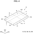
- FIG. 4 is a schematic perspective view of a stage according to an embodiment
- FIG. 5 is a schematic cross-sectional view taken along line V-V′ of FIG. 4 ;
- FIG. 6 is an enlarged schematic view of region A of FIG. 5 ;
- FIG. 7 is a schematic cross-sectional view taken along line VII-VII′ of FIG. 4 ;
- FIG. 8 is a view schematically showing particles and fine particles located inside a chamber
- FIG. 9 is an enlarged schematic view of region B of FIG. 8 ;
- FIG. 10 is a view schematically showing a flow of particles and fine particles with the movement of a stage
- FIG. 11 is an enlarged schematic view of region C of FIG. 10 ;
- FIG. 12 is a cross-sectional view schematically illustrating a portion of a display device manufactured using the manufacturing apparatus according to an embodiment
- FIG. 13 is a schematic perspective view of a stage according to another embodiment
- FIG. 14 is a schematic cross-sectional view of a stage according to still another embodiment.
- FIG. 15 is a schematic cross-sectional view of a stage according to still another embodiment.
- FIG. 16 is a schematic cross-sectional view of a stage according to still another embodiment
- FIG. 17 is a schematic cross-sectional view of a stage according to still another embodiment.
- FIG. 18 is a schematic cross-sectional view of a stage according to still another embodiment.
- spatially relative terms “below”, “beneath”, “lower”, “above”, “upper”, or the like, may be used herein for ease of description to describe the relations between one element or component and another element or component as illustrated in the drawings. It will be understood that the spatially relative terms are intended to encompass different orientations of the device in use or operation, in addition to the orientation depicted in the drawings. For example, in the case where a device illustrated in the drawing is turned over, the device positioned “below” or “beneath” another device may be placed “above” another device. Accordingly, the illustrative term “below” may include both the lower and upper positions. The device may also be oriented in other directions and thus the spatially relative terms may be interpreted differently depending on the orientations.
- first”, “second”, etc. may be used herein to describe various elements, these elements, should not be limited by these terms. These terms may be used to distinguish one element from another element. Thus, a first element discussed below may be termed a second element without departing from teachings of one or more embodiments. The description of an element as a “first” element may not require or imply the presence of a second element or other elements.
- the terms “first”, “second”, etc. may also be used herein to differentiate different categories or sets of elements. For conciseness, the terms “first”, “second”, etc. may represent “first-category (or first-set)”, “second-category (or second-set)”, etc., respectively.
- overlap may include layer, stack, face or facing, extending over, covering or partly covering or any other suitable term as would be appreciated and understood by those of ordinary skill in the art.
- “About” or “approximately” as used herein is inclusive of the stated value and means within an acceptable range of deviation for the particular value as determined by one of ordinary skill in the art, considering the measurement in question and the error associated with measurement of the particular quantity (i.e., the limitations of the measurement system). For example, “about” may mean within one or more standard deviations, or within ⁇ 30%, 20%, 5% of the stated value.
- FIG. 1 is a diagram schematically illustrating a manufacturing apparatus according to an embodiment.
- FIG. 2 is a schematic perspective view of a stage and a moving part according to an embodiment.
- FIG. 3 is a schematic diagram explaining a laser irradiation process according to an embodiment.
- a manufacturing apparatus 1 may include a laser module 10 , an optical system 20 , a chamber 30 and a stage part STU.
- the manufacturing apparatus 1 is an apparatus capable of crystallizing a thin film by irradiating an amorphous thin film on a target substrate S with a laser beam, and an excimer laser annealing (ELA) apparatus will be described as an example.
- ELA excimer laser annealing
- the laser module 10 may emit a laser beam LB capable of crystallizing, particularly, an amorphous silicon thin film in a laser irradiation process.
- the laser beam LB may heat the amorphous silicon thin film to a temperature lower than a melting point of the amorphous silicon thin film.
- the crystalline silicon thin film is crystallized at a temperature lower than the melting point, abnormal protrusions formed at grain boundaries can be reduced, thereby improving crystallinity.
- the optical system 20 may allow the laser beam LB emitted from the laser module 10 to reach the target substrate S inside the chamber 30 .
- the optical system 20 may be disposed above the chamber 30 (on one side of a third direction DR 3 ) outside the chamber 30 .
- the optical system 20 may be spaced apart from the chamber 30 by a distance.
- a laser irradiation process may be performed while the target substrate S moves along a first direction DR 1 in a state where the optical system 20 is fixed.
- the chamber 30 may be internally empty, and provide therein a space in which a stage 40 , a moving part 50 and the like may be disposed.
- the chamber 30 may provide a space in which the laser irradiation process is performed.
- the chamber 30 may have a rectangular parallelepiped shape, but is not limited thereto and may have various shapes.
- a heat treatment atmosphere and/or a vacuum atmosphere may be formed inside the chamber 30 .
- the chamber 30 may be combined with a heater (not shown) to form a heat treatment atmosphere, and may be combined with a vacuum module (not shown) to form a vacuum atmosphere.
- the chamber 30 may include a light transmission window 31 and a substrate inlet 32 .
- the light transmission window 31 may transmit the laser beam LB of a specific wavelength, and allow the laser beam LB emitted from the laser module 10 disposed above the chamber 30 to enter the chamber 30 .
- the laser beam LB emitted from the laser module 10 disposed outside the chamber 30 may be incident into the chamber 30 through the light transmission window 31 .
- the light transmission window 31 may be disposed on the upper surface of the chamber 30 , but is not limited thereto.
- the chamber 30 is illustrated as including one light transmission window 31 in the drawing, the disclosure is not limited thereto and the chamber 30 may include multiple light transmission windows 31 .
- a chamber window protection part (not shown) including a protection window (not shown) for shielding the light transmission window 31 may be further disposed on the upper surface of the chamber 30 .
- the substrate inlet 32 may allow the target substrate S outside the chamber 30 to enter the chamber 30 or to discharge the target substrate S from the inside of the chamber 30 to the outside. In other words, the target substrate S may pass through the substrate inlet 32 to enter the chamber 30 or may be discharged to the outside of the chamber 30 .
- the substrate inlet 32 may be formed at one side surface of the chamber 30 , but is not limited thereto.
- the chamber 30 may further include, at one side thereof, the substrate inlet 32 through which the target substrate S may be introduced into the chamber 30 , and a substrate discharge port (not shown) for discharging to the outside the target substrate S on which the laser irradiation process is completed.
- the stage part STU may support the target substrate S and move the target substrate S.
- the stage part STU may include the stage 40 and the moving part 50 .
- the stage 40 may be disposed inside the chamber 30 .
- the stage 40 may provide a space in which the target substrate S can be stably placed and may support the target substrate S.
- the target substrate S may be mounted on the stage 40 .
- the stage 40 may fix the target substrate S mounted on the stage 40 using a chucking means (not shown).
- the chucking means (not shown) may fix the target substrate S by using vacuum, static electricity and/or van der Waals force.
- the stage 40 may move or rotate in a state where the target substrate S may be stably placed, thereby adjusting the position and direction of the target substrate S to which the laser beam is to be irradiated. Accordingly, the laser beam LB emitted from the laser module 10 may reach a desired region of the target substrate S.
- the stage 40 may further include a substrate support (not shown) and a rotating shaft guide (not shown) connected to the substrate support (not shown) to rotate the substrate support (not shown). By the rotation of the substrate support (not shown), the target substrate S mounted on the stage 40 may be rotated.
- Side surfaces 43 a and 43 b of the stage 40 (see FIG. 4 ) disposed on a side and another side of the stage 40 in the first direction DR 1 may be rounded to be convex toward the outside of the stage 40 . Edges may not be formed at first and second boundaries BD 1 and BD 2 (see FIG. 4 ) where an upper surface 41 (see FIG. 4 ) and the side surfaces 43 a and 43 b (see FIG. 4 ) of the stage 40 meet. Accordingly, foreign matter (or particles P and fine particles MP) (see FIGS. 8 to 11 ) located above the stage 40 can be controlled, and the reliability and yield of the laser irradiation process can be improved. A detailed description thereof will be given later.
- the target substrate S may be mounted, as a target of laser irradiation, on the stage 40 .
- the target substrate S may be moved from the outside to the inside of the chamber 30 by a robot arm or the like.
- An amorphous silicon thin film may be deposited on the target substrate S by another process performed outside the chamber 30 and the target substrate S with the amorphous silicon thin film deposited thereon may be moved into the chamber 30 .
- the disclosure is not limited thereto, and the process of depositing the amorphous silicon thin film may be performed in the chamber 30 in which the laser irradiation process may be performed.
- the target substrate S may have a smaller area than the stage 40 .
- An edge of the target substrate S may be located in an inner region of the stage 40 .
- the entire area of the target substrate S may overlap the stage 40 .
- the target substrate S may occupy substantially the center of the stage 40 .
- the target substrate S may constitute, for example, a flat substrate applied to a display device or the like.
- the display device may include, but are not limited to, an organic light emitting display device, a micro LED display device, a nano LED display device, a quantum dot light emitting display device, a liquid crystal display device, a plasma display device, a field emission display device, an electrophoretic display device, and an electrowetting display device.
- the target substrate S may be a glass substrate or a flexible substrate.
- the flexible substrate may be any of a polyethylene terephthalate (PET) film, a polypropylene (PP) film, a polyethylene (PE) film, a polyimide (PI) film, a polystyrene (PS) film, a polycarbonate (PC) film, a polyethylene naphthalate (PEN) film, a cyclic olefin copolymer (COC) film, an acryl film, or a combination thereof.
- PET polyethylene terephthalate
- PP polypropylene
- PE polyethylene
- PI polyimide
- PS polystyrene
- PC polycarbonate
- PEN polyethylene naphthalate
- COC cyclic olefin copolymer
- At least one element area TA may be formed on the upper surface of the target substrate S.
- An amorphous silicon thin film may be deposited on the element area TA.
- the element area TA may be divided into sub-element areas, which may have a smaller area.
- the disclosure is not limited thereto, and the amorphous silicon thin film deposited on the target substrate S may not be divided into the element area(s) TA, and the entire target substrate S may be formed as the element area TA.
- the amorphous silicon thin film may be deposited on the entire area of the target substrate S.
- the amorphous silicon thin film deposited on the target substrate S may be crystallized by the laser beam LB emitted from the laser module 10 .
- the laser beam LB may be irradiated in a line form onto the target substrate S. While the laser beam LB is irradiated, the target substrate S may be moved horizontally in a direction (e.g., the first direction DR 1 ) perpendicular to the line of the laser beam LB by the stage 40 and/or the moving part 50 . Accordingly, the laser beam LB may be irradiated onto the entire surface of the target substrate S.
- the amorphous silicon thin film may be crystallized into a crystalline silicon thin film over the entire surface of the target substrate S and/or the entire surface of the element area TA.
- the target substrate S on which the crystallization step may be completed may be returned to the horizontal movement (e.g., in the first direction DR 1 ) by the stage 40 and/or the moving part 50 , and discharged to the outside of the chamber 30 through the substrate inlet 32 .
- the amorphous silicon thin film may be crystallized, various elements necessary for operating the flat panel display device may be implemented in the element area TA.
- Various elements formed in the target substrate S and the element area TA may form a flat substrate of the display device.
- the moving part 50 may be disposed below the stage 40 .
- the moving part 50 may be combined with the stage 40 to move the stage 40 in the first direction DR 1 and/or a second direction DR 2 .
- the moving part 50 may include a first moving member 51 , a second moving member 52 , a sliding member 53 and a cable duct 54 .
- the first moving member 51 may extend in the first direction DR 1 and may be implemented as a pair of two rails spaced apart from each other.
- the first moving member 51 may move the second moving member 52 , the stage 40 and the substrate S mounted on the stage 40 to a side and another side in the first direction DR 1 .
- the second moving member 52 may be disposed between the first moving members 51 .
- the second moving member 52 may extend in the second direction DR 2 and may connect the pair of first moving members 51 .
- the second moving member 52 moves to a side and another side in the first direction DR 1 along the first moving members 51 .
- the second moving member 52 may move the stage 40 to a side and another side in the second direction DR 2 by an air bearing (not shown) provided on the lower surface thereof.
- the second moving member 52 may move in the first direction DR 1 along the first moving member 51
- the stage 40 located above the second moving member 52 may move in the second direction DR 2 along the second moving member 52
- the stage 40 may move in the second direction DR 2 as well as the first direction DR 1 by the first moving member 51 and the second moving member 52 .
- the target substrate S mounted on the stage 40 may be located at an appropriate position through the above-described horizontal rotational movement of the substrate support (not shown) in not only the first direction DR 1 but also the second direction DR 2 during the laser irradiation process.
- the sliding member 53 may extend from the second moving member 52 to be connected to the first moving member 51 .
- the sliding member 53 may be implemented as a pair of members spaced apart from each other. The sliding member 53 allows the second moving member 52 to move along the first moving member 51 to a side and another side in the first direction DR 1 .
- the cable duct 54 may be disposed between the pair of sliding members 53 .
- the cable duct 54 may be a cable protection housing that may collect cables for supplying various control currents to the first and second moving members 51 and 52 of the stage 40 .
- the cable duct 54 may be connected by the sliding member 53 to move along with the movement of the sliding member 53 .
- a second moving member bearing (not shown), a stage bearing (not shown) and the substrate support (not shown) provided in the moving part 50 are mechanically operated, splittable foreign matter (or particles P and fine particles MP (see FIGS. 8 to 11 )) may be generated, which may cause a process failure. Further, in a process of loading the target substrate S into the chamber 30 , external foreign matter (or particles P and fine particles MP (see FIGS. 8 to 11 )) may enter the chamber 30 .
- FIG. 4 is a schematic perspective view of a stage according to an embodiment.
- FIG. 5 is a schematic cross-sectional view taken along line V-V of FIG. 4 .
- FIG. 6 is an enlarged schematic view of region A of FIG. 5 .
- FIG. 7 is a schematic cross-sectional view taken along line VII-VII′ of FIG. 4 .
- the stage 40 may include an upper surface 41 , a lower surface 42 opposite to the upper surface 41 , and side surfaces 43 extending to the upper surface 41 and the lower surface 42 .
- the upper surface 41 may be a portion on which the target substrate S may be mounted and may be a surface facing the target substrate S.
- the upper surface 41 may face not only the target substrate S but also the light transmission window 31 (see FIG. 1 ).
- the upper surface 41 may be located above the lower surface 42 (on one side of the third direction DR 3 ).
- the upper surface 41 may be formed in a substantially flat shape.
- the lower surface 42 may be a surface opposite to the upper surface 41 and may face the moving part 30 disposed below the stage 40 .
- the lower surface 42 may be located above the upper surface 41 (on another side of the third direction DR 3 ).
- the lower surface 42 may be formed in a substantially flat shape. Although not limited thereto, the shape and size of the lower surface 42 may be the same as the shape and size of the upper surface 41 , and the lower surface 42 may overlap the upper surface 41 in the third direction DR 3 .
- the side surfaces 43 may extend the upper surface 41 to the lower surface 42 .
- the side surfaces 43 may include a first side surface 43 a , a second side surface 43 b , a third side surface 43 c , and a fourth side surface 43 d .
- the first side surface 43 a refers to a portion located on one side of the stage 40 in the first direction DR 1 and extending in the second direction DR 2 .
- the second side surface 43 b refers to a portion located on another side of the stage 40 in the first direction DR 1 and extending in the second direction DR 2 .
- the third side surface 43 c refers to a portion located on one side of the stage 40 in the second direction DR 2 and extending in the first direction DR 1 .
- the fourth side surface 43 d refers to a portion located on another side of the stage 40 in the second direction DR 2 and extending in the first direction DR 1 .
- the side surfaces e.g., the first side surface 43 a and the second side surface 43 b ) disposed on a side and another side of the stage 40 in the moving direction (e.g., the first direction DR 1 ) may be formed in a round shape.
- the side surfaces 43 a , 43 b , 43 c and 43 d may be formed in a round shape.
- the side surfaces e.g., the first side surface 43 a and the second side surface 43 b ) may be formed in a convex shape toward the outside of the stage 40 .
- the side surfaces 43 a , 43 b , 43 c and 43 d may be formed in a substantially flat shape.
- first side surface 43 a and the second side surface 43 b may extend from the upper surface 41 to the outside of the stage 40 and may be curved to be extended to the lower surface 42 .
- first side surface 43 a and the second side surface 43 b may connect the two surfaces 41 and 42 between the upper surface 41 and the lower surface 42 .
- the first side surface 43 a and the second side surface 43 b may be formed as a portion of the circumference of circle C in cross-sectional view.
- each of the first side surface 43 a and the second side surface 43 b may be formed as half of the circumference of the circle C, i.e., the circumference of a semicircle.
- the disclosure is not limited thereto, and the first side surface 43 a and the second side surface 43 b may be formed as a portion of the circumference of, e.g., an ellipse in cross-sectional view.
- the first side surface 43 a and the second side surface 43 b may be symmetric with each other, may be formed in the same shape, and may include the same curvature.
- the length of a diameter R of the circle C may be about 30 mm or more or about 50 mm or more.
- the radius of curvature of the circle C may be about 15 mm or more or about 25 mm or more.
- the length of the diameter R of the circle C may be equal to the thickness (width in the third direction DR 3 ) of the stage 40 .
- Portions where the first side surface 43 a and the second side surface 43 b meet the upper surface 41 may be referred to as a first boundary BD 1 and a second boundary BD 2 , respectively. Portions where the first side surface 43 a and the second side surface 43 b meet the lower surface 42 may be referred to as a third boundary BD 3 and a fourth boundary BD 4 , respectively.
- the first side surface 43 a and the second side surface 43 b may be rounded at the first boundary BD 1 and the second boundary BD 2 .
- the stage 40 may not have edges formed at the first boundary BD 1 and the second boundary BD 2 . Although not limited thereto, in the stage 40 , the first side surface 43 a and the second side surface 43 b may be rounded at the third boundary BD 3 and the fourth boundary BD 4 .
- a slope of an imaginary tangent line TL in contact with an arbitrary point PT located on the first side surface 43 a may vary continuously as the arbitrary point PT moves toward the first boundary BD 1 .
- an angle ⁇ a between the imaginary tangent line TL in contact with the arbitrary point PT located on the first side surface 43 a in the cross section and an imaginary extension line EL extending from the upper surface 41 may increase continuously as the arbitrary point PT approaches the first boundary BD 1 from the outermost point of the first side surface 43 a .
- the angle ⁇ a may converge to about 180°.
- the angle ⁇ a refers to an obtuse angle formed between the imaginary extension line EL and the imaginary tangent line TL at the arbitrary point PT located on the first side surface 43 a in a region between the first boundary BD 1 and the outermost point of the first side surface 43 a .
- first boundary BD 1 and the first side surface 43 a have been described, but the above description may also be applied to the second boundary BD 2 and the second side surface 43 b.
- Portions where the third side surface 43 c and the fourth side surface 43 d meet the upper surface 41 may be referred to as a fifth boundary BD 5 and a sixth boundary BD 6 , respectively.
- an angle ⁇ 2 between the third side surface 43 c and the upper surface 41 may be smaller than an angle ⁇ 1 between the first side surface 43 a and the upper surface 41 at the first boundary BD 1 where the first side surface 43 a and the upper surface 41 meet.
- the angle ⁇ 2 between the third side surface 43 c and the upper surface 41 at the fifth boundary BD 5 may be a right angle.
- the fifth boundary BD 5 and the third side surface 43 c have been described, but the above description may also be applied to the sixth boundary BD 6 and the fourth side surface 43 d.
- the stage 40 may further include a main part MS, a first sub-part SSa located on one side of the main part MS in the first direction DR 1 , and a second sub-part SSb located on another side of the main part MS in the first direction DR 1 .
- a first imaginary plane PL 1 an imaginary plane extending from the first boundary BD 1 to the third boundary BD 3 at the shortest distance
- a second imaginary plane PL 2 an imaginary plane extending from the second boundary BD 2 to the fourth boundary BD 4 at the shortest distance.
- the main part MS may be a part on which the target substrate S is mounted, and may be a region located between the first imaginary plane PL 1 and the second imaginary plane PL 2 .
- the upper surface 41 of the main part MS may correspond to the upper surface 41 of the stage 40
- the lower surface 42 of the main part MS may correspond to the lower surface 42 of the stage 40 .
- the first sub-part SSa and the second sub-part SSb may be regions protruding from the main part MS on a side and another side of the main part MS in the first direction DR 1 .
- the first sub-part SSa may be a part disposed outside the main part MS with respect to the first imaginary plane PL 1
- the second sub-part SSb may be a part disposed outside the main part MS with respect to the second imaginary plane PL 2 .
- the main part MS, the first sub-part SSa and the second sub-part SSb may be divided by the first imaginary plane PL 1 and the second imaginary plane PL 2 .
- the outer side surface 43 a of the first sub-part SSa may correspond to the first side surface 43 a of the stage 40
- the outer side surface 43 b of the second sub-part SSb may correspond to the second side surface 43 b of the stage 40 .
- the main part MS, the first sub-part SSa and the second sub-part SSb are illustrated as being integrally formed, but the disclosure is not limited thereto.
- the stage 40 may have no edge at the first boundary BD 1 and the second boundary BD 2 where the upper surface 41 of the stage 40 meets the first side surface 43 a and the second side surface 43 b , and the first side surface 43 a and the second side surface 43 b are formed in a round shape, due to the Coanda effect, it is possible to control the flow of foreign matter (or particles P and fine particles MP (see FIGS. 8 to 11 )). A detailed description thereof will be made with reference to FIGS. 8 to 11 .
- FIG. 8 is a view schematically showing particles and fine particles located inside a chamber.
- FIG. 9 is an enlarged schematic view of region B of FIG. 8 .
- FIG. 10 is a view schematically showing the flow of particles and fine particles with the movement of a stage.
- FIG. 11 is an enlarged schematic view of region C of FIG. 10 .
- FIGS. 8 and 9 show a process of forming fine particles by a laser beam
- FIGS. 10 and 11 show a process in which particles and fine particles flow down the stage by the Coanda effect.
- particles P may be located in the chamber 30 .
- Particles P may be very small in size and very light.
- the inside of the chamber 30 which may be an enclosed space may have a small flow development, and despite the gravity, part of the particles P may float without being accumulated in a lower portion of the chamber 30 .
- part of the particles P may float above the upper surface 41 of the stage 40 .
- the particles P may be deposited on the amorphous silicon thin film and/or the crystallized silicon thin film during the laser irradiation process to contaminate the resultant product of the laser irradiation process.
- Some of the particles P located between the stage 40 and the light transmission window 31 may be micronized by the laser beam LB to be divided into fine particles MP.
- the fine particles MP divided from one particle P may be located in more regions than one particle P, and in more regions, may be deposited on the amorphous silicon thin film and/or the crystallized silicon thin film to contaminate more portions of the resultant product of the laser irradiation process.
- the particles P located above the stage 40 may contaminate the resultant product of the laser irradiation process by themselves, and in case the particles P are micronized by the laser beam LB, the resultant product may be contaminated in more regions, e.g., by the fine particles MP.
- the Coanda effect may occur on the upper surface 41 and the first side surface 43 a of the stage 40 by the shape of the stage 40 described above. Accordingly, the particles P and the fine particles MP located above the stage 40 may travel toward the bottom of the stage 40 .
- a downward airflow descending to the bottom of the stage 40 may be formed at one side of the stage 40 in the first direction DR 1 .
- the particles P and the fine particles MP disposed above the stage 40 may relatively move to one side of the first direction DR 1 .
- the particles P and the fine particles MP disposed above the stage 40 may move along the upper surface 41 and the first side surface 43 a of the stage 40 due to the Coanda effect. Thus, it may generally flow toward the bottom of stage 40 .
- the particles P and the fine particles MP may generally flow toward the bottom of the stage 40 , not only in a region adjacent to the stage 40 , but also in a region separated from the stage 40 by a distance. Further, the downward airflow moving along the upper surface 41 and the first side surface 43 a of the stage 40 by the Coanda effect can suppress or prevent the particles P and the fine particles MP, which may be located at the lower side of the chamber 30 or the bottom of the stage 40 , from rising by the wake formed by the movement of the stage 40 .
- a proportion of the particles P and the fine particles MP located above the stage 40 i.e., above the imaginary extension line EL extending from the upper surface of the stage 40 may be about 15% or less or about 11% or less of the total particles P and fine particles MP.
- the stage 40 may have no edge at the first boundary BD 1 (see FIG. 4 ) and the second boundary BD 2 (see FIG. 4 ) where the upper surface 41 (see FIG. 4 ) of the stage 40 (see FIG. 4 ) may meet the first side surface 43 a (see FIG. 4 ) and the second side surface 43 b (see FIG. 4 ) and the first side surface 43 a (see FIG. 4 ) and the second side surface 43 b (see FIG. 4 ) may be rounded. Therefore, it may be possible to reduce the number of the particles P and the fine particles MP located above the stage 40 , and also to reduce the contamination that may be caused by the particles P and the fine particles MP. Accordingly, the reliability and yield of the laser irradiation process can be improved.
- the manufacturing apparatus described so far may be used for manufacturing a display device, and a manufacturing method of the display device also falls within the scope of the disclosure.
- a display device that can be manufactured using the manufacturing apparatus 1 according to an embodiment will be described with reference to FIG. 12 .
- FIG. 12 is a cross-sectional view schematically illustrating a portion of a display device manufactured using the manufacturing apparatus according to an embodiment.
- a display device 60 manufactured by the manufacturing apparatus 1 may include a lower member 61 , a display panel 62 , and a touch member 63 , a polarizing member 64 and a cover window 65 .
- the lower member 61 , the display panel 62 , the touch member 63 , the polarizing member 64 and the cover window 65 may be sequentially stacked on each other.
- At least one coupling member such as an adhesive layer or a tackifying layer may be disposed between the stacked members to couple the adjacent stacked members.
- another layer may be further disposed between the respective layers, and some of the stacked members may be omitted.
- the display panel 62 may be a panel for displaying a screen or an image.
- Examples of the display panel may include not only a self-luminous display panel such as an organic light emitting display (OLED) panel, an inorganic electroluminescence (EL) display panel, a quantum dot (QED) display panel, a micro-LED display panel, a nano-LED display panel, a plasma display panel (PDP), a field emission display (FED) panel and a cathode ray tube (CRT) display panel, but also a light receiving display panel such as a liquid crystal display (LCD) panel and an electrophoretic display (EPD) panel.
- OLED organic light emitting display
- EL inorganic electroluminescence
- QED quantum dot
- micro-LED display panel a micro-LED display panel
- nano-LED display panel a nano-LED display panel
- PDP plasma display panel
- FED field emission display
- CRT cathode ray tube
- a light receiving display panel such as a
- the organic light emitting display panel will be described as an example of the display panel, and the organic light emitting display panel applied to the embodiment will be simply referred to as the display panel 62 unless special distinction is required.
- the embodiment is not limited to the organic light emitting display panel, and other display panels mentioned above or known in the art may be applied within the scope of the same technical ideas.
- the display panel 62 may include a base substrate SUB 1 , a buffer layer SUB 2 , a semiconductor layer ACT, a first insulating layer ILL a first gate conductive layer 621 , a second insulating layer IL 2 , a second gate conductive layer 622 , a third insulating layer IL 3 , a data conductive layer 623 , a fourth insulating layer IL 4 , an anode electrode ANO, a pixel defining layer PDL including an opening exposing the anode electrode ANO, a light emitting layer EML disposed in the opening of the pixel defining layer PDL, a cathode electrode CAT disposed on the light emitting layer EML and the pixel defining layer PDL, and a thin film encapsulation layer EN disposed on the cathode electrode CAT.
- Each of the layers described above may consist of a single layer, or a stack of multiple layers. Other layers may be further disposed between the layers.
- the base substrate SUB 1 may support respective layers disposed thereon.
- the base substrate SUB 1 may be made of an insulating material such as a polymer resin or an inorganic material such as glass or quartz.
- the buffer layer SUB 2 may be disposed on the base substrate SUB 1 .
- the buffer layer SUB 2 may include silicon nitride, silicon oxide, silicon oxynitride, or the like.
- the semiconductor layer ACT may be disposed on the buffer layer SUB 2 .
- the semiconductor layer ACT forms a channel of a thin film transistor of a pixel.
- the semiconductor layer ACT may include polycrystalline silicon obtained by crystallizing amorphous silicon included in the amorphous silicon thin film by the manufacturing apparatus 1 (see FIG. 1 ).
- the semiconductor layer ACT may be obtained by crystallizing and patterning all of the amorphous silicon disposed over the entire region of the target substrate S (see FIG. 3 ) and/or the entire region of the element area TA (see FIG. 3 ), or may be obtained by first patterning the amorphous silicon thin film and then crystallizing the patterned amorphous silicon thin film.
- the semiconductor layer ACT may include an amorphous silicon region (not shown) in which amorphous silicon is disposed and a polycrystalline silicon region (not shown) in which polycrystalline silicon is disposed.
- the first insulating layer IL 1 may be disposed on the semiconductor layer ACT.
- the first insulating layer IL 1 may be a gate insulating layer having a gate insulating function.
- the first gate conductive layer 621 may be disposed on the first insulating layer IL 1 .
- the first gate conductive layer 621 may include a gate electrode GAT of the thin film transistor of the pixel, a scan line connected thereto and a first electrode CE 1 of a storage capacitor.
- the second insulating layer IL 2 may be disposed on the first gate conductive layer 621 .
- the second insulating layer IL 2 may be an interlayer insulating layer or a second gate insulating layer.
- the second gate conductive layer 622 may be disposed on the second insulating layer IL 2 .
- the second gate conductive layer 622 may include a second electrode CE 2 of the storage capacitor.
- the third insulating layer IL 3 may be disposed on the second gate conductive layer 622 .
- the third insulating layer IL 3 may be an interlayer insulating layer.
- the data conductive layer 623 may be disposed on the third insulating layer IL 3 .
- the data conductive layer 623 may include a first electrode SD 1 , a second electrode SD 2 and a first power line ELVDDE of the thin film transistor of the pixel.
- the first electrode SD 1 and the second electrode SD 2 of the thin film transistor may be electrically connected to a source region and a drain region of the semiconductor layer ACT via contact holes passing through the third insulating layer IL 3 , the second insulating layer IL 2 and the first insulating layer IL 1 .
- the fourth insulating layer IL 4 may be disposed on the data conductive layer 623 .
- the fourth insulating layer IL 4 covers the data conductive layer 623 .
- the fourth insulating layer IL 4 may be a via layer.
- the anode electrode ANO may be disposed on the fourth insulating layer IL 4 .
- the anode electrode ANO may be a pixel electrode provided for each pixel.
- the anode electrode ANO may be electrically connected to the second electrode SD 2 of the thin film transistor via the contact hole passing through the fourth insulating layer IL 4 .
- the anode electrode ANO may have a stacked structure formed by stacking a material layer having a high work function, such as indium tin oxide (ITO), indium zinc oxide (IZO), zinc oxide (ZnO) and indium oxide (In2O3), and a reflective material layer such as silver (Ag), magnesium (Mg), aluminum (Al), platinum (Pt), lead (Pb), gold (Au), nickel (Ni), neodymium (Nd), iridium (Ir), chromium (Cr), lithium (Li), calcium (Ca), or a mixture thereof, but is not limited thereto.
- the layer having a high work function may be disposed above the reflective material layer and disposed closer to the light emitting layer EML.
- the anode electrode ANO may have a multilayer structure such as ITO/Mg, ITO/MgF, ITO/Ag and ITO/Ag/ITO, but is not limited thereto.
- the pixel defining layer PDL may be disposed on the anode electrode ANO.
- the pixel defining layer PDL may be disposed on the anode electrode ANO and may include an opening exposing the anode electrode ANO.
- Emission areas EMA and non-emission areas NEM may be distinguished by the pixel defining layer PDL and the openings of the pixel defining layer PDL.
- a spacer 627 may be disposed on the pixel defining layer PDL.
- the spacer 627 may serve to maintain a gap with a structure disposed thereabove.
- the light emitting layer EML is disposed on the anode electrode ANO exposed by the pixel defining layer PDL.
- the light emitting layer EML may include an organic material layer.
- the organic material layer of the light emitting layer may include an organic light emitting layer, and may further include a hole injecting/transporting layer and/or an electron injecting/transporting layer.
- the cathode electrode CAT may be disposed on the light emitting layer EML.
- the cathode electrode CAT may be a common electrode disposed over the entire surface without distinguishing the pixels.
- Each of the anode electrode ANO, the light emitting layer EML and the cathode electrode CAT may constitute an organic light emitting element.
- the cathode electrode CAT may include a material layer having a low work function, such as Li, Ca, LiF/Ca, LiF/Al, Al, Mg, Ag, Pt, Pd, Ni, Au Nd, Ir, Cr, BaF, Ba or a compound or mixture thereof (e.g., a mixture of Ag and Mg).
- the cathode electrode CAT may further include a transparent metal oxide layer disposed on the material layer having a low work function.
- the thin film encapsulation layer EN may include a first inorganic film EN 1 , a first organic film EN 2 and a second inorganic film EN 3 , and may be disposed on the cathode electrode CAT.
- the first inorganic film EN 1 and the second inorganic film EN 3 may be in contact with each other at an end portion of the thin film encapsulation layer EN.
- the first organic film EN 2 may be encapsulated by the first inorganic film EN 1 and the second inorganic film EN 3 .
- Each of the first inorganic film EN 1 and the second inorganic film EN 3 may include silicon nitride, silicon oxide, silicon oxynitride, or the like.
- the first organic film EN 2 may include an organic insulating material.
- the touch member 63 may be disposed on the display panel 62 .
- the touch member 63 may sense a touch input.
- the touch member 63 may be provided as a panel or a film separate from the display panel 62 as illustrated, and may be attached onto the display panel 62 , but the touch member 63 may be provided in the form of a touch layer inside the display panel 62 .
- the polarizing member 64 may be disposed on the touch member 63 .
- the polarizing member 64 polarizes the light passing therethrough.
- the polarizing member 64 may serve to reduce the reflection of external light.
- the cover window 65 may be disposed on the touch member 63 .
- the cover window 65 serves to cover and protect the display panel 62 .
- the cover window 65 may be made of a transparent material.
- the cover window 65 may include, for example, glass, plastic, or a combination thereof.
- the lower member 61 may be disposed below the display panel 62 .
- the lower member 61 may perform a light blocking function.
- the lower member 61 may block light from entering the display panel 62 from the outside. Further, the lower member 61 may perform a shock absorbing function beyond the light blocking function.
- FIG. 13 is a schematic perspective view of a stage according to another embodiment.
- the embodiment is different from the embodiment of FIG. 4 in that among the four side surfaces 43 a , 43 b , 43 c _ 1 and 43 d _ 1 of a stage 40 _ 1 , third and fourth side surfaces 43 c _ 1 and 43 d _ 1 , which are disposed on a side and another side of the stage 40 _ 1 in the second direction DR 2 , may be formed in a round shape.
- the stage 40 _ 1 of the embodiment among the four side surfaces 43 a , 43 b , 43 c _ 1 and 43 d _ 1 of the stage 40 _ 1 , not only the first and second side surfaces 43 a and 43 b disposed on a side and another side of the stage 40 _ 1 in the first direction DR 1 , but also the third side surface 43 c _ 1 and the fourth side surface 43 d _ 1 disposed on a side and another side of the stage 40 _ 1 in the second direction DR 2 may protrude outward from the stage 40 _ 1 and be formed in a round shape.
- the third side surface 43 c _ 1 and the fourth side surface 43 d _ 1 may be formed in a shape of a portion of the circumference of a circle in cross-sectional view.
- the four side surfaces 43 a , 43 b , 43 c _ 1 and 43 d _ 1 formed in a round shape may be extended to each other by corner portions EG disposed between the four side surfaces 43 a , 43 b , 43 c _ 1 and 43 d _ 1 .
- the corner portions EG may be disposed between the four side surfaces 43 a , 43 b , 43 c _ 1 and 43 d _ 1 .
- the corner portion EG may also protrude outward from the stage 40 _ 1 and be formed in a round shape.
- the round shape of the corner portion EG may correspond to the round shape of the four side surfaces 43 a , 43 b , 43 c _ 1 and 43 d _ 1 .
- Portions where the third side surface 43 c _ 1 and the fourth side surface 43 d _ 1 meet the upper surface 41 of the stage 40 _ 1 may be referred to as a third boundary BD 3 _ 1 and a fourth boundary BD 4 _ 1 , respectively.
- the stage 40 _ 1 may have no edge at the third boundary BD 3 _ 1 and the fourth boundary BD 4 _ 1 .
- Foreign matter inside the chamber 30 can be controlled by the downward airflow according to the movement of the stage 40 _ 1 due to the Coanda effect, thereby improving the reliability and yield of the laser irradiation process.
- foreign matter inside the chamber 30 can be controlled by the downward airflow due to the Coanda effect, thereby further improving the reliability and yield of the laser irradiation process.
- FIG. 14 is a schematic cross-sectional view of a stage according to still another embodiment.
- the embodiment is different from the embodiment of FIG. 5 in that a lower surface 42 _ 2 of a stage 40 _ 2 does not have the same shape and size as the upper surface 41 .
- the lower surface 42 _ 2 of the stage 40 _ 2 may include a first region OV_ 2 overlapping the upper surface 41 in the third direction DR 3 , and a second region NOV_ 2 extending from the first region OV_ 2 to a side and another side of the first direction DR 1 and protruding outward from the stage 40 _ 2 .
- a width L of the second region NOV_ 2 in the first direction DR 1 may be the same as the thickness (width in the third direction DR 3 ) of the stage 40 _ 2 .
- Each of a first side surface 43 a _ 2 and a second side surface 43 b _ 2 may be formed as a portion corresponding to one quarter (1 ⁇ 4) of the circumference of a circle C_ 2 .
- the thickness of the stage 40 _ 2 may be about 30 mm or more or about 50 mm or more.
- a diameter R_ 2 of the circle C_ 2 may be about 60 mm or more or about 100 mm or more.
- the stage 40 _ 2 may have no edge at the first boundary BD 1 and the second boundary BD 2 , and foreign matter inside the chamber 30 (see FIG. 1 ) can be controlled by the downward airflow according to the movement of the stage 40 _ 2 due to the Coanda effect, thereby improving the reliability and yield of the laser irradiation process.
- FIG. 15 is a schematic cross-sectional view of a stage according to still another embodiment.
- the embodiment is different from the embodiment of FIG. 5 in that only a portion of each of a first side surface 43 a _ 3 and a second side surface 43 b _ 3 of a stage 40 _ 3 is formed in a round shape.
- the first side surface 43 a _ 3 and the second side surface 43 b _ 3 of the stage 40 _ 3 may include first regions Ra_ 3 and Rb_ 3 formed in a round shape and second regions Sa_ 3 and Sb_ 3 excluding the first regions Ra_ 3 and Rb_ 3 , respectively.
- Each of the first regions Ra_ 3 and Rb_ 3 of the first side surface 43 a _ 3 and the second side surface 43 b _ 3 may be formed as a portion of the circumference of a circle C_ 3 , although not limited thereto.
- the second regions Sa_ 3 and Sb_ 3 may have a substantially flat shape.
- Boundaries where the first regions Ra_ 3 and Rb_ 3 and the second regions Sa_ 3 and Sb_ 3 of the first side surface 43 a _ 3 and the second side surface 43 b _ 3 meet are referred to as a third boundary BD 3 _ 3 and a fourth boundary BD 4 _ 3 , respectively.
- the third boundary BD 3 _ 3 and the fourth boundary BD 4 _ 3 may be located on the first side surface 43 a _ 3 and the second side surface 43 b _ 3 , respectively.
- a region between the first boundary BD 1 and the third boundary BD 3 _ 3 may be the first region Ra_ 3 of the first side surface 43 a _ 3
- a region between the second boundary BD 2 and the fourth boundary BD 4 _ 3 may be the first region Rb_ 3 of the second side surface 43 b _ 3
- the first region Ra_ 3 of the first side surface 43 a _ 3 may be extended to the upper surface 41 at the first boundary BD 1
- the first region Rb_ 3 of the second side surface 43 b _ 3 may be extended to the upper surface 41 at the second boundary BD 2 .
- the first region Ra_ 3 of the first side surface 43 a _ 3 may be extended to the second region Sa_ 3 of the first side surface 43 a _ 3 at the third boundary BD 3 _ 3
- the first region Rb_ 3 of the second side surface 43 b _ 3 may be extended to the second region Sb_ 3 of the second side surface 43 b _ 3 at the fourth boundary BD 4 _ 3
- the second regions Sa_ 3 and Sb_ 3 of the first side surface 43 a _ 3 and the second side surface 43 b _ 3 may be extended to the lower surface 42 .
- the stage 40 _ 3 may have no edge at the first boundary BD 1 and the second boundary BD 2 . Although not limited thereto, the stage 40 _ 3 may have no edge at the third boundary BD 3 _ 3 and the fourth boundary BD 4 _ 3 . Therefore, the stage 40 _ 3 can control foreign matter inside the chamber 30 (see FIG. 1 ) by the downward airflow according to the movement of the stage 40 _ 3 due to the Coanda effect, thereby improving the reliability and yield of the laser irradiation process.
- FIG. 16 is a schematic cross-sectional view of a stage according to still another embodiment.
- the embodiment is different from the embodiment of FIG. 5 in that a thickness W 1 (width in the third direction DR 3 ) of a main part MS_ 4 of a stage 40 _ 4 is different from a thickness W 2 (width in the third direction DR 3 ) of first and second sub-parts SSa_ 4 and SSb_ 4 of the stage 40 _ 4 .
- the stage 40 _ 4 may include the main part MS_ 4 , the first sub-part SSa_ 4 and the second sub-part SSb_ 4 , and the thickness W 2 of the first and second sub-parts SSa_ 4 and SSb_ 4 may be smaller than the thickness W 1 of the main part MS_ 4 .
- the first sub-part SSa_ 4 and the second sub-part SSb_ 4 may be formed to protrude from the main part MS_ 4 to a side and another side of the first direction DR 1 , and protrude from portions of the main part MS_ 4 on a side and another side of the first direction DR 1 .
- a first side surface 43 a _ 4 and a second side surface 43 b _ 4 of the stage 40 _ 4 may include first regions Ra_ 4 and Rb_ 4 formed in a round shape and second regions Sa_ 4 and Sb_ 4 formed in a substantially flat shape, respectively.
- the first regions Ra_ 4 and Rb_ 4 of the first side surface 43 a _ 4 and the second side surface 43 b _ 4 may be located outside the main part MS_ 4 with respect to the first imaginary plane PL 1 and the second imaginary plane PL 2 , respectively.
- the second regions Sa_ 4 and Sb_ 4 of the first side surface 43 a _ 4 and the second side surface 43 b _ 4 may be located on the first imaginary plane PL 1 and the second imaginary plane PL 2 , respectively.
- the first regions Ra_ 3 and Rb_ 4 may have a radius R 4 .
- the stage 40 _ 4 may have no edge at the first boundary BD 1 and the second boundary BD 2 . Therefore, the stage 40 _ 4 can control foreign matter inside the chamber 30 (see FIG. 1 ) by the downward airflow according to the movement of the stage 40 _ 4 due to the Coanda effect, thereby improving the reliability and yield of the laser irradiation process.
- FIG. 17 is a schematic cross-sectional view of a stage according to still another embodiment.
- a stage 40 _ 5 may include a main part MS_ 5 , a first sub-part SSa_ 5 and a second sub-part SSb_ 5 which are not integrally formed.
- the stage 40 _ 5 includes the main part MS_ 5 , the first sub-part SSa_ 5 and the second sub-part SSb_ 5 , and the main part MS_ 5 , the first sub-part SSa_ 5 and the second sub-part SSb_ 5 may be formed separately, and assembled by being combined with each other.
- the side surfaces located on a side and another side of the main part MS_ 5 in the first direction DR 1 are referred to as a first outer surface OTa_ 5 and a second outer surface OTb_ 5 , respectively.
- One surface of the first sub-part SSa_ 5 facing the first outer surface OTa_ 5 of the main part MS_ 5 may be referred to as a first inner surface INa_ 5
- one surface of the second sub-part SSb_ 5 facing the second outer surface OTb_ 5 of the main part MS_ 5 may be referred to as a second inner surface INb_ 5 .
- the first outer surface OTa_ 5 and the second outer surface OTb_ 5 of the main part MS_ 5 may be in contact with the first inner surface INa_ 5 of the first sub-part SSa_ 5 and the second inner surface INb_ 5 of the second sub-part SSb_ 5 , respectively.
- the main part MS_ 5 , the first sub-part SSa_ 5 and the second sub-part SSb_ 5 may be coupled to each other by bolt coupling. However, without being limited thereto, they may be coupled to each other, for example, by welding, hook coupling, or bonding using an adhesive member.
- the stage 40 _ 5 may have no edge at the first boundary BD 1 and the second boundary BD 2 . Therefore, the stage 40 _ 5 can control foreign matter inside the chamber 30 (see FIG. 1 ) by the downward airflow according to the movement of the stage 40 _ 5 due to the Coanda effect, thereby improving the reliability and yield of the laser irradiation process.
- FIG. 18 is a schematic cross-sectional view of a stage according to still another embodiment.
- a stage 40 _ 6 is configured such that a main part MS_ 6 may be separated by a distance from each of a first sub-part SSa_ 6 and a second sub-part SSb_ 6 .
- the stage 40 _ 6 includes the main part MS_ 6 , the first sub-part SSa_ 6 and the second sub-part SSb_ 6 , and the components are separately formed and assembled.
- the first sub-part SSa_ 6 and the second sub-part SSb_ 6 may cover a first outer surface OTa_ 6 and a second outer surface OTb_ 6 of the main part MS_ 6
- the first outer surface OTa_ 6 and the second outer surface OTb_ 6 of the main part MS_ 6 may be in contact with a portion of a first inner surface INa_ 6 of the first sub-part SSa_ 6 and a portion of a second inner surface INa_ 6 of the second sub-part SSb_ 6 , respectively.
- Another portion of the first inner surface INa_ 6 of the first sub-part SSa_ 6 and another portion of the second inner surface INb_ 6 of the second sub-part SSb_ 6 may be separated by a distance from the first outer surface OTa_ 6 and the second outer surface OTb_ 6 of the main part MS_ 6 , respectively.
- the stage 40 _ 6 may have no edge at the first boundary BD 1 and the second boundary BD 2 . Therefore, the stage 40 _ 6 can control foreign matter inside the chamber 30 (see FIG. 1 ) by the downward airflow according to the movement of the stage 40 _ 6 due to the Coanda effect, thereby improving the reliability and yield of the laser irradiation process.
Landscapes
- Engineering & Computer Science (AREA)
- Chemical & Material Sciences (AREA)
- Crystallography & Structural Chemistry (AREA)
- Manufacturing & Machinery (AREA)
- Microelectronics & Electronic Packaging (AREA)
- Recrystallisation Techniques (AREA)
- Physics & Mathematics (AREA)
- Optics & Photonics (AREA)
- Health & Medical Sciences (AREA)
- Toxicology (AREA)
Abstract
Description
Claims (14)
Priority Applications (1)
| Application Number | Priority Date | Filing Date | Title |
|---|---|---|---|
| US17/966,256 US11887998B2 (en) | 2020-02-07 | 2022-10-14 | Manufacturing apparatus and manufacturing method using the same |
Applications Claiming Priority (2)
| Application Number | Priority Date | Filing Date | Title |
|---|---|---|---|
| KR10-2020-0014935 | 2020-02-07 | ||
| KR1020200014935A KR20210101360A (en) | 2020-02-07 | 2020-02-07 | Manufacturing apparatus and manufacturing method using thereof |
Related Child Applications (1)
| Application Number | Title | Priority Date | Filing Date |
|---|---|---|---|
| US17/966,256 Division US11887998B2 (en) | 2020-02-07 | 2022-10-14 | Manufacturing apparatus and manufacturing method using the same |
Publications (2)
| Publication Number | Publication Date |
|---|---|
| US20210249452A1 US20210249452A1 (en) | 2021-08-12 |
| US11488991B2 true US11488991B2 (en) | 2022-11-01 |
Family
ID=77178502
Family Applications (2)
| Application Number | Title | Priority Date | Filing Date |
|---|---|---|---|
| US16/938,426 Active US11488991B2 (en) | 2020-02-07 | 2020-07-24 | Manufacturing apparatus and manufacturing method using the same |
| US17/966,256 Active US11887998B2 (en) | 2020-02-07 | 2022-10-14 | Manufacturing apparatus and manufacturing method using the same |
Family Applications After (1)
| Application Number | Title | Priority Date | Filing Date |
|---|---|---|---|
| US17/966,256 Active US11887998B2 (en) | 2020-02-07 | 2022-10-14 | Manufacturing apparatus and manufacturing method using the same |
Country Status (3)
| Country | Link |
|---|---|
| US (2) | US11488991B2 (en) |
| KR (1) | KR20210101360A (en) |
| CN (1) | CN113257710A (en) |
Families Citing this family (2)
| Publication number | Priority date | Publication date | Assignee | Title |
|---|---|---|---|---|
| KR20220106900A (en) * | 2021-01-22 | 2022-08-01 | 삼성디스플레이 주식회사 | Cassette for loading panel and substrate processign method using the same |
| KR20240115950A (en) * | 2023-01-19 | 2024-07-26 | 삼성디스플레이 주식회사 | Display device |
Citations (5)
| Publication number | Priority date | Publication date | Assignee | Title |
|---|---|---|---|---|
| KR100700821B1 (en) | 2005-08-26 | 2007-03-27 | 삼성에스디아이 주식회사 | Crystallization Method and Manufacturing Method of Light-emitting Display Device Using the Method |
| WO2010049696A2 (en) * | 2008-10-30 | 2010-05-06 | Mtt Technologies Limited | Additive manufacturing apparatus and method |
| US9496163B2 (en) * | 2013-12-05 | 2016-11-15 | Samsung Electronics Co., Ltd. | Carrier and method of fabricating semiconductor device using the same |
| CN106133187A (en) * | 2014-03-24 | 2016-11-16 | 艾克斯特朗欧洲公司 | Substrate holder at two wide sides deviated from mutually supporting substrates respectively of substrate holder |
| US20170040352A1 (en) | 2015-08-07 | 2017-02-09 | Samsung Display Co., Ltd. | Laser annealing apparatus and method of manufacturing display apparatus by using the same |
Family Cites Families (10)
| Publication number | Priority date | Publication date | Assignee | Title |
|---|---|---|---|---|
| KR20040023916A (en) * | 2002-09-12 | 2004-03-20 | 엘지.필립스 엘시디 주식회사 | Laser annealing apparatus and method |
| CN101752457B (en) * | 2008-12-18 | 2011-11-02 | 北京北方微电子基地设备工艺研究中心有限责任公司 | Method and equipment for manufacturing solar battery |
| KR20110002664U (en) * | 2009-09-09 | 2011-03-16 | 디엔씨엔지니어링 주식회사 | Air-Floating Flat Panel Conveyor |
| JP4904420B2 (en) * | 2009-09-28 | 2012-03-28 | パナソニック株式会社 | Wiping apparatus for inkjet and wiping method using the same |
| JP5779756B2 (en) * | 2011-11-24 | 2015-09-16 | 株式会社昭和真空 | Vapor deposition equipment |
| JP6100487B2 (en) * | 2012-08-20 | 2017-03-22 | 株式会社Screenホールディングス | Substrate processing equipment |
| US9011207B2 (en) * | 2012-10-29 | 2015-04-21 | Wayne O. Duescher | Flexible diaphragm combination floating and rigid abrading workholder |
| KR101600382B1 (en) * | 2014-05-12 | 2016-03-08 | 제트에스-핸들링 게엠베하 | Non-contact type device for substrate gripping |
| JP6412466B2 (en) * | 2015-06-02 | 2018-10-24 | 東京エレクトロン株式会社 | Substrate processing apparatus and substrate processing method |
| US9905607B2 (en) * | 2015-07-28 | 2018-02-27 | General Electric Company | Radiation detector fabrication |
-
2020
- 2020-02-07 KR KR1020200014935A patent/KR20210101360A/en not_active Ceased
- 2020-07-24 US US16/938,426 patent/US11488991B2/en active Active
-
2021
- 2021-02-04 CN CN202110155132.1A patent/CN113257710A/en active Pending
-
2022
- 2022-10-14 US US17/966,256 patent/US11887998B2/en active Active
Patent Citations (5)
| Publication number | Priority date | Publication date | Assignee | Title |
|---|---|---|---|---|
| KR100700821B1 (en) | 2005-08-26 | 2007-03-27 | 삼성에스디아이 주식회사 | Crystallization Method and Manufacturing Method of Light-emitting Display Device Using the Method |
| WO2010049696A2 (en) * | 2008-10-30 | 2010-05-06 | Mtt Technologies Limited | Additive manufacturing apparatus and method |
| US9496163B2 (en) * | 2013-12-05 | 2016-11-15 | Samsung Electronics Co., Ltd. | Carrier and method of fabricating semiconductor device using the same |
| CN106133187A (en) * | 2014-03-24 | 2016-11-16 | 艾克斯特朗欧洲公司 | Substrate holder at two wide sides deviated from mutually supporting substrates respectively of substrate holder |
| US20170040352A1 (en) | 2015-08-07 | 2017-02-09 | Samsung Display Co., Ltd. | Laser annealing apparatus and method of manufacturing display apparatus by using the same |
Also Published As
| Publication number | Publication date |
|---|---|
| KR20210101360A (en) | 2021-08-19 |
| CN113257710A (en) | 2021-08-13 |
| US11887998B2 (en) | 2024-01-30 |
| US20210249452A1 (en) | 2021-08-12 |
| US20230037161A1 (en) | 2023-02-02 |
Similar Documents
| Publication | Publication Date | Title |
|---|---|---|
| KR102472092B1 (en) | Organic light emitting display apparatus and method of manufacturing thereof | |
| US11569474B2 (en) | Organic light-emitting diode (OLED) display and method of fabricating the same | |
| US20190115415A1 (en) | Display device | |
| KR101065408B1 (en) | Touch display | |
| US11296238B2 (en) | Thin-film transistor substrate and display apparatus comprising the same | |
| US11887998B2 (en) | Manufacturing apparatus and manufacturing method using the same | |
| CN107492563B (en) | Display device | |
| EP2963687A1 (en) | Organic electroluminescent device | |
| US12232387B2 (en) | Display apparatus including layer with a plurality of parts having different electrical conductivities on emission layers | |
| US20050189535A1 (en) | Organic light-emitting device and method of fabricating the same | |
| US8426861B2 (en) | Organic light emitting display device | |
| US8237168B2 (en) | Organic light emitting display device | |
| CN110993811B (en) | Display device | |
| KR20160090455A (en) | Manufacturing method of flexible display device | |
| KR20110104794A (en) | OLED display and touch display device including the same | |
| US10770679B2 (en) | Display apparatus and manufacturing method thereof inlcuding substrate having guide mark disposed overlapping sealing member | |
| US20240389390A1 (en) | Display apparatus and apparatus and method of manufacturing the same | |
| CN108695368B (en) | display screen | |
| CN113445003A (en) | Mask assembly, apparatus for manufacturing display apparatus, and method of manufacturing display apparatus | |
| CN112289824B (en) | Display apparatus | |
| US10515579B2 (en) | Display device | |
| US11565354B2 (en) | Stage for cutting substrate and substrate cutting device | |
| US8962357B2 (en) | Method for manufacturing organic light emitting diode display | |
| US20180019437A1 (en) | Organic light emitting display device | |
| US12550507B2 (en) | Display apparatus |
Legal Events
| Date | Code | Title | Description |
|---|---|---|---|
| AS | Assignment |
Owner name: SAMSUNG DISPLAY CO., LTD., KOREA, REPUBLIC OF Free format text: ASSIGNMENT OF ASSIGNORS INTEREST;ASSIGNORS:JUNG, SOO YOUNG;KIM, JOON HYUNG;KIM, JEONG MOK;AND OTHERS;REEL/FRAME:053310/0974 Effective date: 20200629 |
|
| FEPP | Fee payment procedure |
Free format text: ENTITY STATUS SET TO UNDISCOUNTED (ORIGINAL EVENT CODE: BIG.); ENTITY STATUS OF PATENT OWNER: LARGE ENTITY |
|
| STPP | Information on status: patent application and granting procedure in general |
Free format text: RESPONSE TO NON-FINAL OFFICE ACTION ENTERED AND FORWARDED TO EXAMINER |
|
| STPP | Information on status: patent application and granting procedure in general |
Free format text: NON FINAL ACTION MAILED |
|
| STPP | Information on status: patent application and granting procedure in general |
Free format text: RESPONSE TO NON-FINAL OFFICE ACTION ENTERED AND FORWARDED TO EXAMINER |
|
| STPP | Information on status: patent application and granting procedure in general |
Free format text: FINAL REJECTION MAILED |
|
| STPP | Information on status: patent application and granting procedure in general |
Free format text: RESPONSE AFTER FINAL ACTION FORWARDED TO EXAMINER |
|
| STPP | Information on status: patent application and granting procedure in general |
Free format text: NOTICE OF ALLOWANCE MAILED -- APPLICATION RECEIVED IN OFFICE OF PUBLICATIONS |
|
| STPP | Information on status: patent application and granting procedure in general |
Free format text: PUBLICATIONS -- ISSUE FEE PAYMENT VERIFIED |
|
| STCF | Information on status: patent grant |
Free format text: PATENTED CASE |
|
| MAFP | Maintenance fee payment |
Free format text: PAYMENT OF MAINTENANCE FEE, 4TH YEAR, LARGE ENTITY (ORIGINAL EVENT CODE: M1551); ENTITY STATUS OF PATENT OWNER: LARGE ENTITY Year of fee payment: 4 |