US11488941B2 - Light-emitting device - Google Patents
Light-emitting device Download PDFInfo
- Publication number
- US11488941B2 US11488941B2 US16/861,412 US202016861412A US11488941B2 US 11488941 B2 US11488941 B2 US 11488941B2 US 202016861412 A US202016861412 A US 202016861412A US 11488941 B2 US11488941 B2 US 11488941B2
- Authority
- US
- United States
- Prior art keywords
- light
- emitting
- region
- substrate
- emitting device
- Prior art date
- Legal status (The legal status is an assumption and is not a legal conclusion. Google has not performed a legal analysis and makes no representation as to the accuracy of the status listed.)
- Active, expires
Links
Images


Classifications
-
- H—ELECTRICITY
- H01—ELECTRIC ELEMENTS
- H01L—SEMICONDUCTOR DEVICES NOT COVERED BY CLASS H10
- H01L25/00—Assemblies consisting of a plurality of semiconductor or other solid state devices
- H01L25/03—Assemblies consisting of a plurality of semiconductor or other solid state devices all the devices being of a type provided for in a single subclass of subclasses H10B, H10D, H10F, H10H, H10K or H10N, e.g. assemblies of rectifier diodes
- H01L25/04—Assemblies consisting of a plurality of semiconductor or other solid state devices all the devices being of a type provided for in a single subclass of subclasses H10B, H10D, H10F, H10H, H10K or H10N, e.g. assemblies of rectifier diodes the devices not having separate containers
- H01L25/075—Assemblies consisting of a plurality of semiconductor or other solid state devices all the devices being of a type provided for in a single subclass of subclasses H10B, H10D, H10F, H10H, H10K or H10N, e.g. assemblies of rectifier diodes the devices not having separate containers the devices being of a type provided for in group H10H20/00
- H01L25/0753—Assemblies consisting of a plurality of semiconductor or other solid state devices all the devices being of a type provided for in a single subclass of subclasses H10B, H10D, H10F, H10H, H10K or H10N, e.g. assemblies of rectifier diodes the devices not having separate containers the devices being of a type provided for in group H10H20/00 the devices being arranged next to each other
-
- H10W90/00—
-
- H01L33/36—
-
- H01L33/505—
-
- H01L33/52—
-
- H01L33/58—
-
- H01L33/60—
-
- H—ELECTRICITY
- H10—SEMICONDUCTOR DEVICES; ELECTRIC SOLID-STATE DEVICES NOT OTHERWISE PROVIDED FOR
- H10H—INORGANIC LIGHT-EMITTING SEMICONDUCTOR DEVICES HAVING POTENTIAL BARRIERS
- H10H20/00—Individual inorganic light-emitting semiconductor devices having potential barriers, e.g. light-emitting diodes [LED]
- H10H20/80—Constructional details
- H10H20/83—Electrodes
-
- H—ELECTRICITY
- H10—SEMICONDUCTOR DEVICES; ELECTRIC SOLID-STATE DEVICES NOT OTHERWISE PROVIDED FOR
- H10H—INORGANIC LIGHT-EMITTING SEMICONDUCTOR DEVICES HAVING POTENTIAL BARRIERS
- H10H20/00—Individual inorganic light-emitting semiconductor devices having potential barriers, e.g. light-emitting diodes [LED]
- H10H20/80—Constructional details
- H10H20/84—Coatings, e.g. passivation layers or antireflective coatings
- H10H20/841—Reflective coatings, e.g. dielectric Bragg reflectors
-
- H—ELECTRICITY
- H10—SEMICONDUCTOR DEVICES; ELECTRIC SOLID-STATE DEVICES NOT OTHERWISE PROVIDED FOR
- H10H—INORGANIC LIGHT-EMITTING SEMICONDUCTOR DEVICES HAVING POTENTIAL BARRIERS
- H10H20/00—Individual inorganic light-emitting semiconductor devices having potential barriers, e.g. light-emitting diodes [LED]
- H10H20/80—Constructional details
- H10H20/85—Packages
- H10H20/851—Wavelength conversion means
- H10H20/8514—Wavelength conversion means characterised by their shape, e.g. plate or foil
-
- H—ELECTRICITY
- H10—SEMICONDUCTOR DEVICES; ELECTRIC SOLID-STATE DEVICES NOT OTHERWISE PROVIDED FOR
- H10H—INORGANIC LIGHT-EMITTING SEMICONDUCTOR DEVICES HAVING POTENTIAL BARRIERS
- H10H20/00—Individual inorganic light-emitting semiconductor devices having potential barriers, e.g. light-emitting diodes [LED]
- H10H20/80—Constructional details
- H10H20/85—Packages
- H10H20/852—Encapsulations
-
- H—ELECTRICITY
- H10—SEMICONDUCTOR DEVICES; ELECTRIC SOLID-STATE DEVICES NOT OTHERWISE PROVIDED FOR
- H10H—INORGANIC LIGHT-EMITTING SEMICONDUCTOR DEVICES HAVING POTENTIAL BARRIERS
- H10H20/00—Individual inorganic light-emitting semiconductor devices having potential barriers, e.g. light-emitting diodes [LED]
- H10H20/80—Constructional details
- H10H20/85—Packages
- H10H20/855—Optical field-shaping means, e.g. lenses
- H10H20/856—Reflecting means
-
- H—ELECTRICITY
- H01—ELECTRIC ELEMENTS
- H01L—SEMICONDUCTOR DEVICES NOT COVERED BY CLASS H10
- H01L25/00—Assemblies consisting of a plurality of semiconductor or other solid state devices
- H01L25/16—Assemblies consisting of a plurality of semiconductor or other solid state devices the devices being of types provided for in two or more different subclasses of H10B, H10D, H10F, H10H, H10K or H10N, e.g. forming hybrid circuits
- H01L25/167—Assemblies consisting of a plurality of semiconductor or other solid state devices the devices being of types provided for in two or more different subclasses of H10B, H10D, H10F, H10H, H10K or H10N, e.g. forming hybrid circuits comprising optoelectronic devices, e.g. LED, photodiodes
-
- H01L2933/0083—
-
- H—ELECTRICITY
- H10—SEMICONDUCTOR DEVICES; ELECTRIC SOLID-STATE DEVICES NOT OTHERWISE PROVIDED FOR
- H10H—INORGANIC LIGHT-EMITTING SEMICONDUCTOR DEVICES HAVING POTENTIAL BARRIERS
- H10H20/00—Individual inorganic light-emitting semiconductor devices having potential barriers, e.g. light-emitting diodes [LED]
- H10H20/80—Constructional details
- H10H20/85—Packages
- H10H20/851—Wavelength conversion means
-
- H—ELECTRICITY
- H10—SEMICONDUCTOR DEVICES; ELECTRIC SOLID-STATE DEVICES NOT OTHERWISE PROVIDED FOR
- H10H—INORGANIC LIGHT-EMITTING SEMICONDUCTOR DEVICES HAVING POTENTIAL BARRIERS
- H10H20/00—Individual inorganic light-emitting semiconductor devices having potential barriers, e.g. light-emitting diodes [LED]
- H10H20/80—Constructional details
- H10H20/872—Periodic patterns for optical field-shaping, e.g. photonic bandgap structures
Definitions
- the disclosure relates to a light-emitting device and an electronic device, and particularly to a light-emitting diode (LED) light-emitting device and an LED electronic device.
- LED light-emitting diode
- a light-emitting device including a light-emitting unit and an optical layer.
- the light-emitting unit includes a light-emitting chip and an encapsulation disposed thereon.
- the optical layer is disposed on the light-emitting unit, the optical layer having a first region overlapping the light-emitting chip in a top view direction of the light-emitting device and a second region not overlapping the light-emitting chip in the top view direction of the light-emitting device, wherein the transmittance of the first region is less than the transmittance of the second region.
- FIG. 1A is a schematic view of some elements of a light-emitting device in some embodiments of the present disclosure.
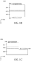
- FIGS. 1B and 1C are cross-sectional views of light-emitting chips in some embodiments of the present disclosure.
- FIGS. 2A and 2B are schematic views showing the relationship between the light-emitting intensity of light-emitting units and viewing angles of the present disclosure.
- FIGS. 3A to 3C are schematic views of light-emitting devices in some embodiments of the present disclosure.
- FIG. 4 is a schematic view of some embodiments of the present disclosure.
- FIGS. 5A to 5D are top views of some embodiments of the present disclosure.
- FIGS. 6A and 6B are top views of some embodiments of the present disclosure.
- FIG. 7 is a schematic view of some embodiments of the present disclosure.
- FIG. 8 is a schematic view showing the reflectivity of an optical layer in different positions in some embodiments of the present disclosure.
- FIGS. 9A and 9B are schematic views of some elements of light-emitting devices in some embodiments of the present disclosure.
- FIGS. 10A to 10E are schematic views of some elements of light-emitting devices in some embodiments of the present disclosure.
- FIG. 11 is a schematic view of some elements of a light-emitting device in some embodiments of the present disclosure.
- FIG. 12 is a schematic view of some elements of a light-emitting device in some embodiments of the present disclosure.
- first and second features are formed in direct contact
- additional features may be formed between the first and second features, such that the first and second features may not be in direct contact
- the present disclosure may repeat reference numerals and/or letters in the various examples. This repetition is for the purpose of simplicity and clarity and does not in itself dictate a relationship between the various embodiments and/or configurations discussed.
- the formation of a feature on, connected to, and/or coupled to another feature in the present disclosure that follows may include embodiments in which the features are formed in direct contact, and may also include embodiments in which additional features may be formed with interposing the features, such that the features may not be in direct contact.
- spatially relative terms such as “vertically,” “above,” “over,” “below,”, “bottom,” etc.
- the terms “about” and “substantially” typically mean a range of +/ ⁇ 20% of the stated value, more typically +/ ⁇ 10% of the stated value, more typically +/ ⁇ 5% of the stated value, more typically +/ ⁇ 3% of the stated value, more typically +/ ⁇ 2% of the stated value, more typically +/ ⁇ 1% of the stated value and even more typically +/ ⁇ 0.5% of the stated value.
- the stated value of the present disclosure is an approximate value. When there is no specific description, the stated value still implies the meaning of “about” or “substantially”.
- the phrase “in a range between a first value and a second value” or “in a range from a first value to a second value” indicates that the range includes the first value, the second value, and other values between them.
- FIG. 1A is a schematic view of some elements of a light-emitting device 1 in some embodiments of the present disclosure.
- the light-emitting device 1 in some embodiments of the present disclosure may include some elements of a flexible display, a touch display, a curved display, or a free shape display, but it is not limited thereto.
- the light-emitting device 1 may mainly include a substrate 10 , a plurality of light-emitting units 20 disposed on the substrate 10 , and optical layers 30 disposed on the light-emitting units 20 .
- the substrate 10 may be an array substrate, such as a driving substrate for the light-emitting units 20 .
- the substrate 10 may include thin-film transistors (TFT) or driving circuits (not shown), but it is not limited thereto.
- the driving circuit may be an active driving circuit or a passive driving circuit.
- the driving circuit may include transistors (such as switching transistor or driving transistor), data lines, scanning lines, conductive pads, dielectric layers or other circuits, but it is not limited thereto.
- the switching transistor may control the light-emitting units 20 to be activated or deactivated.
- the driving circuit may couple to integrated circuits (IC) or microchips to control the light-emitting unit 20 .
- IC integrated circuits
- the material of the substrate 10 may include glass, quartz, sapphire, polycarbonate (PC), polyimide (PI), polyethylene terephthalate (PET), rubber, glass fiber, ceramic, other suitable materials or a combination thereof, but it is not limited thereto.
- the substrate 10 may include metal-glass fiber composite board, printed circuit board (PCB), flexible printed circuit (FPC), but it is not limited thereto.
- the light-emitting unit 20 may act as a light source of the light-emitting device 1 , and may mainly include an encapsulation substrate 22 , an encapsulation 24 disposed on the encapsulation substrate 22 , and a light-emitting chip assembly 26 disposed in the encapsulation substrate 24 .
- the material of the encapsulation substrate 2 may be bismaleimide triazine (BT) resin, polyimide, epoxy glass fiber, ceramic, etc., but the present disclosure is not limited thereto.
- circuits may be disposed in/on the encapsulation substrate 22 to make the light-emitting chip assembly 26 electrically connect to the substrate 10 through the encapsulation substrate 22 .
- the material of the encapsulation 24 may be silicon, epoxy resin, etc., but the present disclosure is not limited thereto.
- the encapsulation 24 may act as a protective layer to protect the light-emitting chip assembly 26 disposed therein.
- the encapsulation 24 may be formed from chemical vapor deposition (CVD), coating, printing, inkjet printing, compression molding, other suitable methods or a combination thereof, or the encapsulation 24 may be formed by one or more photolithography processes and etching processes.
- CVD chemical vapor deposition
- coating printing, inkjet printing, compression molding, other suitable methods or a combination thereof
- etching processes other suitable methods or a combination thereof
- the light-emitting chip assembly 26 may include a plurality of light-emitting chips (such as light-emitting chip 26 A, light-emitting chip 26 B and light-emitting chip 26 C in FIG. 1A ) which can emitting light having an identical color or different colors (such as red, green, blue, or white lights) but the present disclosure is not limited thereto.
- the light-emitting chip 26 A, light-emitting chip 26 B and light-emitting chip 26 C may include organic light-emitting diode (OLED), quantum dot light-emitting diode (QLED/QDLED), light-emitting diode (LED).
- the light-emitting diode may include micro LED or mini LED, etc.
- FIGS. 1B and 1C show cross-sectional views of the light-emitting chip 26 A (or the light-emitting chip 26 B or the light-emitting chip 26 C) in some embodiments of the present disclosure.
- the light-emitting chip 26 A may be a vertical type light-emitting chip, according to some embodiments.
- the light-emitting chip 26 A may be a flip-chip type light-emitting chip, according to other embodiments.
- the present disclosure is not limited thereto.
- the light-emitting chip 26 A (or the light-emitting chip 26 B or the light-emitting chip 26 C) may include a first semiconductor layer 261 , a second semiconductor layer 262 , and an active layer 263 .
- the active layer 263 may be disposed between the first semiconductor layer 261 and the second semiconductor layer 262 .
- one of the first semiconductor layer 261 and the second semiconductor layer 262 may be used to provide and/or transport electrons, and the other may be used to provide and/or transport electron holes.
- the first semiconductor layer 261 and the second semiconductor layer 262 may include a n-type semiconductor material and a p-type semiconductor material, respectively.
- the first semiconductor layer 261 and the second semiconductor layer 262 may include a p-type semiconductor material and a n-type semiconductor material, respectively.
- the n-type semiconductor material may include, but is not limited to, gallium nitride (n-GaN) or aluminum indium phosphide (n-AlInP), which are doped with tetravalent atoms.
- the p-type semiconductor material having may include, but is not limited to, gallium nitride (p-GaN) or aluminum indium phosphide (p-AlInP), which are doped with divalent atoms.
- the active layer 206 may have a quantum well structure.
- the active layer 206 may include a single quantum well (SQW), a multiple quantum well (MQW), a nanowire, other suitable structures, or a combination thereof.
- the material of the active layer 206 may include, but is not limited to, gallium nitride, aluminum indium phosphide (AlInP), indium gallium nitride (InGaN), or a combination thereof, but it is not limited thereto.
- the first semiconductor layer 261 , the second semiconductor layer 262 , and the active layer 263 may be formed by an epitaxial growth process.
- the epitaxial growth process may include, but is not limited to, a molecular beam epitaxy (MBE) process, a liquid phase epitaxy (LPE) process, a solid phase epitaxy (SPE) process, a vapor phase epitaxy (VPE) process, a selective epitaxial growth (SEG) process, a metal organic chemical vapor deposition (MOCVD) process, an atomic layer deposition (ALD) process or a combination thereof.
- MBE molecular beam epitaxy
- LPE liquid phase epitaxy
- SPE solid phase epitaxy
- VPE vapor phase epitaxy
- SEG selective epitaxial growth
- MOCVD metal organic chemical vapor deposition
- ALD atomic layer deposition
- the light-emitting chip 26 A may also include a first electrode layer 264 and a second electrode layer 265 that are disposed on the first semiconductor layer 261 and the second semiconductor layer 262 .
- the first electrode layer 264 and the second electrode layer 265 are disposed on two opposite sides (as shown in FIG. 1B ).
- the first electrode layer 264 and the second electrode layer 265 are disposed on the same side (as shown in FIG. 1C ).
- the first electrode layer 264 and the second electrode layer 265 may be further electrically connected to the signal line (not illustrated) and the driving circuit (not illustrated) of the substrate 10 .
- the material of the first electrode layer 264 and the second electrode layer 265 may include a conductive metal material.
- the conductive metal material may include, but is not limited to, copper (Cu), aluminum (Al), tungsten (W), titanium (Ti), gold (Au), platinum (Pt), nickel (Ni), tin (Sn), indium (In), an alloy thereof, other suitable conductive materials, or a combination thereof, but it is not limited thereto.
- the first electrode layer 264 and/or the second electrode layer 265 may be formed by one or more deposition processes, photolithography processes, and etching processes.
- the deposition process may include a chemical vapor deposition process, a physical vapor deposition process, an electroplating process, an electroless plating process, other suitable processes, or a combination thereof.
- the photolithography process may include photoresist coating (e.g., spin coating), soft baking, hard baking, mask aligning, exposure, post-exposure baking, developing the photoresist, rinsing, drying, or another suitable process.
- the etching process may include a dry etching process, a wet etching process, or another suitable etching process.
- the structure of the light-emitting chip 26 A may be adjusted or additional elements may be disposed in or on the light-emitting chip 26 A according to requirements.
- the light-emitting chip 26 A of the present disclosure is not limited to the structures as described above.
- the optical layer 30 may include, materials having high reflectance, such as metals or other complex materials having different refractive indexes, but the present disclosure is not limited thereto.
- the metals may be silver, aluminum, gold, nickel, another suitable material, or a combination thereof, but it is not limited thereto.
- the complex material may include TiO 2 , SiO 2 , Nb 2 O 5 , Ta 2 O 5 , ZrO 2 , Al 2 O 3 , Y 2 O 3 , MgO, other suitable materials, or a combination thereof, but it is not limited thereto.
- the optical layer 30 may be a distributed Bragg reflector (DBR).
- DBR distributed Bragg reflector
- at least a portion of light may be reflected in an interface between different mediums when light passes through the mediums, and the reflectivity is related to the refractive indexes of the mediums.
- a portion of light reflected by the layers may perform constructive interference and combine with some other portion of the light due to phase angle changing when light passing through the thin films having different refractive indexes, so at least a portion of the light may be reflected and the thin films may form a distributed Bragg reflector.
- the optical layer 30 may be formed of different metals having different transmittances to reflect the light or allow the light passing through.
- the optical layer 30 may also include an omni-directional reflector (ODR) structure.
- the omni-directional reflector structure may include a stack of dielectric material/metal reflective material/dielectric material.
- the dielectric material may include, but is not limited to, silicon oxide (SiO x ), silicon nitride (SiN x ), silicon oxynitride (SiON), aluminum oxide (Al 2 O 3 ), titanium dioxide (TiO 2 ), other suitable materials, or combination thereof, but the present disclosure is not limited thereto.
- the metal reflective material may include, but is not limited to, copper, aluminum, indium, ruthenium, tin, gold, platinum, zinc, silver, titanium, lead, nickel, chromium, magnesium, palladium, an alloy thereof, other suitable materials or a combination thereof, but it is not limited thereto.
- FIGS. 2A and 2B are schematic views showing the relationship between the light-emitting intensity of the light-emitting unit and view angles of the present disclosure.
- the light-emitting unit 20 in FIG. 2A does not have the optical layer 30
- the light-emitting unit 20 in FIG. 2B has the optical layer 30 .
- the light-emitting unit 20 substantially has the highest light-emitting intensity when the viewing angle is 0 degree (i.e.
- the top view direction in which the substrate is being observed here is briefed as “the top view direction” for simplicity in the following paragraphs.
- the optical layer 30 is provided to reflect the light at a small viewing angle (close to the top view direction), so at least a portion of the light may be emitted from the sides where no optical layer 30 is provided, i.e. emitted from the position having a larger viewing angle.
- the highest light-emitting intensity of the light-emitting device in FIG. 2B is not when the viewing angle is at 0 degree (parallel to the top view direction), and the light-emitting intensity may be increased as the viewing angle increases, until a specific angle is reached.
- this angle may be about 60 degrees in FIG. 2B , but the present disclosure is not limited thereto.
- the light-emitting intensity may be decreased as the viewing angle increases. Therefore, the problem of the light-emitting intensity decaying rapidly along the viewing angle may be solved.
- the optical layer 30 may be formed from aforementioned deposition, coating, printing, inkjet printing, compression molding, other suitable methods or a combination thereof, or the optical layer 30 may be formed by one or more photolithography processes and etching processes.
- FIGS. 3A to 3C are schematic views of the light-emitting device 2 A, light-emitting device 2 B, and light-emitting device 2 C in some embodiments of the present disclosure, respectively.
- the light-emitting device 2 A mainly includes a backlight unit B 1 (which includes the substrate 10 , the light-emitting unit 20 A, the optical layer 30 , and an optical film 40 ) and a display layer 42 disposed on the backlight unit B 1 .
- the optical film may be a prism film, a diffusion film, a dual brightness enhancement film (DBEF), a quantum dot film, etc., but it is not limited thereto.
- the optical film 40 may be affixed by mechanisms, adhesives or other methods.
- the display layer 42 may selectively include liquid crystal (LC), quantum dot, fluorescence material, phosphor material, OLED, other display medium, or a combination thereof, but the present disclosure is not limited thereto. Additional adhesive or mechanisms (not shown) may be provided between the substrate 10 and the optical film 40 to connect or affix the substrate 10 and the optical film 40 .
- LC liquid crystal
- QLED organic light-emitting diode
- Additional adhesive or mechanisms may be provided between the substrate 10 and the optical film 40 to connect or affix the substrate 10 and the optical film 40 .
- the light-emitting unit 20 A may have a structure similar to the light-emitting unit 20 , but the present disclosure is not limited thereto.
- the light-emitting unit 20 B of the backlight unit B 2 may include the encapsulation substrate 22 , the encapsulation 24 , and a light-emitting chip 27 disposed in the encapsulation 24 .
- the backlight unit B 2 further includes a wavelength conversion layer 44 disposed on the optical layer 30 .
- the light-emitting chip 27 may provide light having short wavelength to visible light wavelength.
- the range of the wavelength may be between about 10 nm to about 780 nm.
- the present disclosure is not limited thereto.
- the light-emitting chip 27 may provide infrared or far infrared. In some embodiments, the light-emitting chip 27 may provide blue light or ultraviolet (UV), and the wavelength conversion layer 44 may convert the light emitted from the light-emitting chip 27 to the light having the desired wavelength (such red light, green light or white light, but it is not limited thereto). For example, in some embodiments, the wavelength conversion layer 44 may be patterned and disposed corresponding to the light-emitting unit 20 B to convert the lights emitted from different light-emitting chips 27 to lights having different wavelengths.
- UV ultraviolet
- the positions of the optical film 40 and the wavelength conversion layer 44 may be changed, which means that the wavelength conversion layer 44 may be positioned between the optical film 40 and the display layer 42 .
- the wavelength conversion layer 44 may be a light filter to filter light of certain wavelengths, so the light emitted from the light-emitting chip 27 may have the desired wavelength after passing through the wavelength conversion layer 44 .
- the backlight unit B 3 of a light-emitting device 2 C does not have the wavelength conversion layer in the aforementioned embodiments, and the light-emitting chip 27 is covered by an encapsulation 25 having light conversion mediums to make the light-emitting unit 20 C (which includes the encapsulation substrate 22 , the encapsulation 25 and the light-emitting chip 27 ) directly emit light having the desired wavelength (such as red light, green light or white light, but it is not limited thereto).
- the backlight unit B 1 , backlight unit B 2 , and backlight unit B 3 may be, for example, light sources for the display layer 42 to display images.
- the encapsulation 25 may be a light filter as well.
- the encapsulation 25 or the wavelength conversion layer 44 may convert the wavelength of light, such as converting the light emitted from the light-emitting chip 27 to the light having specific wavelength range (i.e. having specific color).
- the encapsulation 25 or the wavelength conversion layer 44 may include base material and particles distributed in the base material.
- the base material may include organic polymer, inorganic polymer, glass, or a combination thereof, but it is not limited thereto.
- the base material may be transparent or translucent.
- the particles may include, but are not limited to, phosphors, quantum dot (QD) materials, organic fluorescent materials, or a combination thereof, but it is not limited thereto.
- the encapsulation 25 or the wavelength conversion layer 44 may include phosphors that can convert the light source into red light, green light, blue light or light having any other suitable color.
- the quantum dot material may have a core-shell structure.
- the core structure may include, but is not limited to, CdSe, CdTe, CdS, ZnS, ZnSe, ZnO, ZnTe, InAs, InP, GaP, other suitable materials or a combination thereof, but it is not limited thereto.
- the shell structure may include, but is not limited to, ZnS, ZnSe, GaN, GaP, other suitable materials or a combination thereof, but it is not limited thereto.
- the encapsulation 25 or the wavelength conversion layer 44 may include scatter particles.
- the scattering particles may have a high reflection coefficient (e.g., greater than 30%). The scattering particles may further increase light absorption efficiency of the quantum dot material or change the light intensity distribution at different viewing angles.
- the material of the scattering particles may include titanium (Ti) or zinc (Zn).
- the scattering particles may include, but are not limited to, titanium dioxide (TiO 2 ), niobium-doped titanium oxide (TNO), zinc oxide (ZnO), zirconium dioxide (ZrO 2 ) or a combination thereof, but the present disclosure is not limited thereto.
- the encapsulation 25 or the wavelength conversion layer 44 may be formed by a chemical vapor deposition process, a coating process, a printing process, an inkjet printing process, compression molding, other suitable processes, or a combination thereof. Moreover, the encapsulation 25 or the wavelength conversion layer 44 may be formed by one or more photolithography processes and etching processes.
- FIG. 4 is a schematic view in some embodiments of the present disclosure, and FIGS. 5A to 5D and FIGS. 6A to 6B are top views of the embodiments having different optical layers.
- the optical layer 30 in FIG. 4 may be substituted by the optical layers in FIGS. 5A to 5D and FIGS. 6A to 6B , depending on design requirements.
- the optical layer 30 A (which equals to the optical layer 30 in FIG. 4 ) may include a first region R 1 and a second region R 2 .
- the first region R 1 may be a region that overlaps the light-emitting chip assembly 26 or the light-emitting chip 27 in the top view direction
- the second region R 2 may be a region that does not overlap the light-emitting chip assembly 26 or the light-emitting chip 27 in the top view direction.
- the first region R 1 is a union of the orthogonal projections of the light-emitting chips of the light-emitting chip assembly 26 or the orthogonal projection of the light-emitting chip 27 .
- the area of the first region R 1 is the sum of the areas of the light-emitting chip 26 A, light-emitting chip 26 B and light-emitting chip 26 C if the light-emitting chip assembly 26 has light-emitting chip 26 A, light-emitting chip 26 B and light-emitting chip 26 C.
- the optical layer 30 A may include optical material 31 A and a plurality of holes 32 A, holes 32 B, and holes 32 C in the optical material 31 A.
- the optical material 31 A may include materials with high reflectance, such as a metal or another complex material having a different refractive index, but the present disclosure is not limited thereto.
- the metal may be silver, aluminum, gold, nickel, another suitable material, or a combination thereof, but it is not limited thereto.
- the complex material may include TiO 2 , SiO 2 , Nb 2 O 5 , Ta 2 O 5 , ZrO 2 , Al 2 O 3 , Y 2 O 3 , MgO, or a combination thereof, but it is not limited thereto.
- the holes 32 C may position in the first region, and the holes 32 A and the holes 32 B may position in the second region R 2 when viewed in the top view direction. More specifically, in the top view, the holes 32 C overlap the light-emitting chip assembly 26 (or the light-emitting chip 27 ), the holes 32 A and the holes 32 B are spaced from the light-emitting chip assembly 26 (or the light-emitting chip 27 ) for a distance, and the distance between the holes 32 B to the light-emitting chip assembly 26 or the light-emitting chip 27 (i.e.
- the shortest distance between the edge of the projection of the holes 32 B and the edge of the projection of the light-emitting chip assembly 26 or the light-emitting chip 27 when viewed in the top view direction) is less than the distance between the holes 32 A to the light-emitting chip assembly 26 or the light-emitting chip 27 .
- the area density of the holes 32 C in the first region R 1 is less than the area density of the holes 32 A and the holes 32 B in the second region R 2 .
- the term “area density” refers to the proportion of the total projection area of the holes (or the gaps, or the light blocking patterns described later) in the per-unit area of the optical layer in the top view direction.
- the area of the first region R 1 is the area of the optical layer that overlaps either the light-emitting chip assembly 26 or the light-emitting chip 27 , when viewed in the top view direction.
- the area of the second region R 2 is the area of the optical layer that does not overlap the light-emitting chip assembly 26 or the light-emitting chip 27 , when viewed in the top view direction. It should be noted that in some embodiments, such as the embodiment shown in FIG.
- the optical layer may be provided continuously, and area of the second region R 2 may be measured within a square region having several millimeters side length rather than measuring the whole optical layer.
- the light-emitting chips of the light-emitting chip assembly 26 may be separated with each other, the first region R 1 may be the portions that overlap the light-emitting chips in the top view direction, and the area of the first region R 1 may be the sum of the areas of the portions that overlap the light-emitting chips.
- the transmittance of the optical layer 30 A may increase from its center to its edge.
- the transmittance of the first region R 1 may be less than the transmittance of the second region R 2 . Therefore, the light emitted from the light-emitting chip assembly 26 or the light-emitting chip 27 to the first region R 1 may tend to be reflected rather than passing through the optical layer to achieve the performance shown in FIG. 2B to solve the problem that the light-emitting intensity decaying rapidly along the viewing angle.
- the intensity of incident light in the present disclosure is defined as the intensity of the light exited from the encapsulation and entering into the optical layer.
- the intensity of emitted light in the present disclosure is defined as the intensity of the light exited from the optical layer.
- the size of the hole 32 A (such as the greatest width) may be greater than the size of the hole 32 B, and the size of the hole 32 B may be greater than the size of the hole 32 C, so the area density of the holes in the first region R 1 is less than the area density of the holes in the second region R 2 .
- the present disclosure is not limited thereto.
- the hole 32 A, hole 32 B, and hole 32 C may have identical sizes, and the area density of the holes may be changed by changing the number of holes per unit area. In other words, there are more holes per unit area in the second region than in the first region, but it is not limited thereto.
- FIGS. 5C and 5D are top views of light-emitting devices in some embodiments of the present disclosure. Rectangular gap 34 A, rectangular gap 34 B, and rectangular gap 34 C are provided on the optical layer 30 B in FIG. 5C , and circular gap 36 A, circular gap 36 B, and circular gap 36 C are provided on the optical layer 30 C in FIG. 5D , such as concentric circles, but the present disclosure is not limited thereto.
- the rectangular gap 34 A or the circular gap 36 A are positioned at the first region R 1
- the rectangular gap 34 B, rectangular gap 34 C or the circular gap 36 B, circular gap 36 C are positioned at the second region R 2 .
- the distance between the rectangular gap 34 B to the first region R 1 i.e.
- the shortest distance between the projection of the rectangular gap 34 B and the projection of the edges of the light-emitting chip assembly 26 or the light-emitting chip 27 in the top view direction, and the distance of other gaps are measured in the same way) is less than the distance between the rectangular gap 34 C and the first region R 1
- the distance between the circular gap 36 B and the first region R 1 is less than the distance between the circular gap 36 C and the first region R 1
- the widths W of the rectangular gap 34 A, rectangular gap 34 B, and rectangular gap 34 C may increase as being farther from the center of the optical layer 30 C (or the optical layer 30 D).
- the area density of the gaps in the first region R 1 may be less than the area density of the gaps in the second region R 2 , and the transmittance of the optical layer 30 B or the optical layer 30 C may increase from the center to the edge, that is, the transmittance of the first region R 1 is less than the transmittance of the second region R 2 . Therefore, the problem of the light-emitting intensity decaying rapidly along the viewing angle may be solved.
- optical material 31 B having high transmittance such as higher than the optical material 31 A
- a plurality of light blocking pattern 38 A, light blocking pattern 38 B, and light blocking pattern 38 C may be disposed in the optical material 31 B.
- the light blocking pattern 38 A, light blocking pattern 38 B, and light blocking pattern 38 C may include reflective material similar to the optical material 31 A, but it is not limited thereto.
- the light blocking pattern 38 A, light blocking pattern 38 B, and light blocking pattern 38 C may have materials that can absorb light.
- the light blocking patterns 38 C may be disposed in the first region R 1 , and the light blocking pattern 38 A and light blocking pattern 38 B may be disposed in the second region R 2 .
- the size of light blocking pattern 38 A e.g. the greatest width
- the size of the light blocking pattern 38 B may be less than the size of the light blocking pattern 38 C to make the area density of the light blocking pattern in the first region R 1 greater than the area density of the light blocking pattern in the second region R 2 . Therefore, the problem of the light-emitting intensity decaying rapidly along the viewing angle may be solved.
- hole 32 A, hole 32 B, hole 32 C, rectangular gap 34 A, rectangular gap 34 B, rectangular gap 34 C, circular gap 36 A, circular gap 36 B, circular gap 36 C, and light blocking pattern 38 A, light blocking pattern 38 B, light blocking pattern 38 C are described in the aforementioned embodiments, but they are only examples, the present disclosure is not limited thereto.
- the holes, gaps, or light blocking patterns may have identical size or more than three kinds of sizes, depending on design requirement.
- the reflectivity of the optical layer in different position may be changed by the different thickness of the optical layer in different regions.
- the optical layer 30 E may has a multilayer structure, and the thickness T 1 of the optical layer 30 E in the first region R 1 is greater than the thickness T 2 of the optical layer 30 E in the second region R 2 , such as more layers of optical layers are provided in the first region.
- the optical layer may be a single layer that has a greater thickness at the center than the edge. As a result, the transmittance of the first region R 1 is less than the transmittance of the second region R 2 to solve the problem that the light-emitting intensity decaying rapidly along the viewing angle.
- the thicknesses of the optical layer in the first region R 1 and in the second region R 2 are respectively defined as the greatest distances from the top surface of the optical layer 30 E in the first region R 1 and in the second region R 2 to the top surface of the light-emitting unit 20 in the top view direction.
- FIG. 8 is a schematic view showing the reflectivity of an optical layer in different positions in some embodiments of the present disclosure, such as the embodiments in FIG. 4 to FIG. 7 .
- the X axis of FIG. 7 corresponds to the position (as along line A-A′ in FIG. 4 , wherein the original point is the center of the light-emitting chip assembly 26 or the light-emitting chip 27 ), and the Y axis of FIG. 7 corresponds to the reflectivity of the optical layer.
- the closer to the center of the light-emitting chip assembly 26 or the light-emitting chip 27 in the X axis the higher the reflectivity of the optical layer.
- the viewing angle is small (near the top view direction of the substrate of the light-emitting device), the light may be reflected by the optical layer more easily and emitted from the position corresponds to a larger viewing angle.
- the light-emitting unit 20 and optical layer 30 may be disposed on a transparent substrate 12 , and a reflective layer 50 may be disposed on the substrate 12 .
- the substrate 12 may include transparent materials such as glass, polyimide, other suitable materials or a combination thereof, but it is not limited thereto.
- the substrate 12 may include thin-film transistor (TFT) or driving circuit (not shown).
- the driving circuit may be active driving circuit or passive driving circuit.
- the driving circuit may include transistors (such as switching transistor or driving transistor), data lines, scanning lines, conductive pads, dielectric layers or another circuit, but it is not limited thereto.
- the reflective layer 50 may include a material having reflective properties.
- the material of the reflective layer 50 may include a metal.
- the metal may include, but is not limited to, copper (Cu), aluminum (Al), indium (In), ruthenium (Ru), tin (Sn), gold (Au), platinum (Pt), zinc (Zn), silver (Ag), titanium (Ti), lead (Pb), nickel (Ni), chromium (Cr), magnesium (Mg), palladium (Pd), an alloy thereof, other suitable materials, or a combination thereof, but it is not limited thereto.
- the material of the reflective layer 50 may further include titanium dioxide, silicon dioxide or a combination thereof.
- the reflective layer 50 and the light-emitting unit 20 may be disposed at an identical side of the substrate 12 (as shown in FIG. 9A ), or the reflective layer 50 and the light-emitting unit 20 may be disposed at different sides of the substrate 12 (as shown in FIG. 9B ), but it is not limited thereto. Therefore, the light emitted to the substrate 12 may be reflected to the display layer (such as the display layer 42 in FIG. 3A ), increasing the brightness of the light-emitting device.
- the reflective layer 50 may be formed from deposition, coating, printing, inkjet printing, compression molding, other suitable methods or a combination thereof, or the reflective layer 50 may be formed by one or more photolithography processes and etching processes.
- FIGS. 10A to 10E are schematic views of some elements of light-emitting devices in some embodiments of the present disclosure.
- the light-emitting chip assembly 26 of the light-emitting device 4 A may be disposed on the substrate 10 , and no encapsulation substrate 22 is provided.
- Driving circuit (not shown) of the light-emitting chip assembly 26 may be provided on the surface of the substrate 10 . As a result, the manufacture process of the light-emitting device 4 A may be simplified.
- the substrate 10 may be substituted by the combination of the transparent substrate 12 and the reflective layer 50 .
- the light-emitting device 4 B, light-emitting device 4 C, light-emitting device 4 D, and light-emitting device 4 E have the transparent substrate 12 and the reflective layer 50 , wherein the reflective layer 50 and the light-emitting chip assembly 26 are disposed on different sides of the substrate 12 in the light-emitting device 4 B and light-emitting device 4 C, and the reflective layer 50 and the light-emitting chip assembly 26 are disposed on an identical side of the substrate 12 in the light-emitting device 4 D and light-emitting device 4 E.
- the optical layer 30 may cover the light-emitting chip assembly 26 and expose a portion of the top surface of the encapsulation 24 (as shown in FIG. 10B ), or the optical layer 30 may cover the entire top surface of the encapsulation 24 (as shown in FIG. 10C ), depending on design requirement.
- more than one emitting chip assemblies 26 may be disposed in an identical encapsulation 24 , such as packaged in an identical encapsulation 24 to simplify the required manufacturing process, but the present disclosure is not limited thereto.
- the emitting chip assemblies 26 are disposed in different encapsulations 24 .
- an additional light guide layer 60 may be provided between the light-emitting chip assembly 26 and the optical layer 30 to make the light emitted from the light-emitting chip assembly 26 uniform.
- the material of the light guide layer may be, for example, plastic, glass, polyimide, sapphire, other suitable materials or a combination thereof, but it is not limited thereto.
- the top surface of the light-emitting chip assembly 26 (the surface away from the substrate 12 ) may directly contact the light guide layer 60 , or a portion of the encapsulation 24 may be positioned between the light-emitting chip assembly 26 and the light guide layer 60 , but it is not limited thereto.
- an additional anti-reflective layer may be disposed on the substrate of the light-emitting device to reduce that the external light is reflected by the substrate to the light-emitting chip and weaken the performance of light-emitting chip.
- an anti-reflective layer 70 is provided on the substrate 10 of the light-emitting device 6 .
- the material of the anti-reflective layer 70 may include low reflectivity material, such as a black photoresist or a light absorptive adhesive, but it is not limited thereto. As a result, the interference due to the light reflection between adjacent light-emitting devices may be reduced, and the lifetime of the light-emitting device may be increased.
- the image quality may be less affected by the reflected ambient light, such as sun light.
- the light-emitting chip assembly 26 of light-emitting device 6 may be pixels to directly show images.
- the anti-reflective layer 70 may be formed from the aforementioned deposition, coating, printing, inkjet printing, compression molding, another suitable method, or a combination thereof.
- the anti-reflective layer 70 may be formed by one or more photolithography processes and etching processes.
- a light-emitting device having an optical layer on the light-emitting unit is provided in some embodiments of the present disclosure.
- the optical layer having different transmittance in different regions the problem of the light-emitting intensity decaying rapidly along the viewing angle may be solved, improving the performance of the light-emitting device. Since the aforementioned embodiments in the disclosure may perform substantially the same function and obtain substantially the same results, some embodiments of the present disclosure may be combined without conflicting with the spirit of the disclosure.
- the light-emitting device may have touch-control functionality, to act as a touch-electronic device.
- the light-emitting device or touch-electronic device in the embodiments of the present disclosure may be applied in any electronic devices with a display screen, such as a display, a mobile phone, a watch, a laptop computer, a video camera, a camera, a mobile navigation device, or a television. These are merely examples, and the applications of the present disclosure are not limited thereto.
- the touch-electronic device of the aforementioned embodiments of the present disclosure may be applied in an electronic device that has an antenna, or in other types of electronic devices.
Landscapes
- Engineering & Computer Science (AREA)
- Power Engineering (AREA)
- Microelectronics & Electronic Packaging (AREA)
- Physics & Mathematics (AREA)
- Condensed Matter Physics & Semiconductors (AREA)
- General Physics & Mathematics (AREA)
- Computer Hardware Design (AREA)
- Led Device Packages (AREA)
- Electroluminescent Light Sources (AREA)
Abstract
Description
Claims (19)
Priority Applications (1)
| Application Number | Priority Date | Filing Date | Title |
|---|---|---|---|
| US16/861,412 US11488941B2 (en) | 2019-05-02 | 2020-04-29 | Light-emitting device |
Applications Claiming Priority (4)
| Application Number | Priority Date | Filing Date | Title |
|---|---|---|---|
| US201962841879P | 2019-05-02 | 2019-05-02 | |
| CN202010017160.2 | 2020-01-08 | ||
| CN202010017160.2A CN111883627A (en) | 2019-05-02 | 2020-01-08 | Light emitting device |
| US16/861,412 US11488941B2 (en) | 2019-05-02 | 2020-04-29 | Light-emitting device |
Publications (2)
| Publication Number | Publication Date |
|---|---|
| US20200350295A1 US20200350295A1 (en) | 2020-11-05 |
| US11488941B2 true US11488941B2 (en) | 2022-11-01 |
Family
ID=73017018
Family Applications (1)
| Application Number | Title | Priority Date | Filing Date |
|---|---|---|---|
| US16/861,412 Active 2040-06-03 US11488941B2 (en) | 2019-05-02 | 2020-04-29 | Light-emitting device |
Country Status (1)
| Country | Link |
|---|---|
| US (1) | US11488941B2 (en) |
Families Citing this family (7)
| Publication number | Priority date | Publication date | Assignee | Title |
|---|---|---|---|---|
| US11594665B2 (en) * | 2019-08-02 | 2023-02-28 | Nichia Corporation | Light-emitting unit and surface-emission light source |
| JP2023011415A (en) * | 2021-07-12 | 2023-01-24 | 創智車電股▲ふん▼有限公司 | Projection image generation device and its head-up display system |
| KR20230055063A (en) * | 2021-10-18 | 2023-04-25 | 삼성전자주식회사 | Display apparatus |
| US12046697B2 (en) | 2021-10-18 | 2024-07-23 | Samsung Electronics Co., Ltd. | Backlight unit including green and blue LEDs and associated distributed bragg reflectors |
| KR20240098733A (en) * | 2022-12-21 | 2024-06-28 | 엘지디스플레이 주식회사 | Display device |
| TWI864594B (en) | 2023-02-15 | 2024-12-01 | 光森科技有限公司 | Light source module |
| US20240322093A1 (en) * | 2023-03-23 | 2024-09-26 | Yenrich Technology Corporation | Light-emitting module |
Citations (7)
| Publication number | Priority date | Publication date | Assignee | Title |
|---|---|---|---|---|
| US20110249215A1 (en) * | 2010-04-13 | 2011-10-13 | Lg Electronics Inc. | Backlight unit and display apparatus comprising the same |
| US20120170253A1 (en) * | 2011-01-05 | 2012-07-05 | Sangtae Park | Display device |
| US20130188114A1 (en) * | 2011-11-28 | 2013-07-25 | Nlt Technologies, Ltd. | Direct type backlight device and liquid crystal display using the same |
| US20150155439A1 (en) * | 2009-09-18 | 2015-06-04 | Soraa, Inc. | High-performance led fabrication |
| US20170059937A1 (en) * | 2013-01-23 | 2017-03-02 | Lg Electronics Inc. | Planar lighting device |
| US20180023784A1 (en) * | 2016-07-20 | 2018-01-25 | Nichia Corporation | Light emitting device |
| CN108803135A (en) | 2017-05-03 | 2018-11-13 | 群创光电股份有限公司 | display device |
-
2020
- 2020-04-29 US US16/861,412 patent/US11488941B2/en active Active
Patent Citations (7)
| Publication number | Priority date | Publication date | Assignee | Title |
|---|---|---|---|---|
| US20150155439A1 (en) * | 2009-09-18 | 2015-06-04 | Soraa, Inc. | High-performance led fabrication |
| US20110249215A1 (en) * | 2010-04-13 | 2011-10-13 | Lg Electronics Inc. | Backlight unit and display apparatus comprising the same |
| US20120170253A1 (en) * | 2011-01-05 | 2012-07-05 | Sangtae Park | Display device |
| US20130188114A1 (en) * | 2011-11-28 | 2013-07-25 | Nlt Technologies, Ltd. | Direct type backlight device and liquid crystal display using the same |
| US20170059937A1 (en) * | 2013-01-23 | 2017-03-02 | Lg Electronics Inc. | Planar lighting device |
| US20180023784A1 (en) * | 2016-07-20 | 2018-01-25 | Nichia Corporation | Light emitting device |
| CN108803135A (en) | 2017-05-03 | 2018-11-13 | 群创光电股份有限公司 | display device |
Non-Patent Citations (1)
| Title |
|---|
| Chinese language office action dated Apr. 19, 2021, issued in application No. CN 202010017160.2. |
Also Published As
| Publication number | Publication date |
|---|---|
| US20200350295A1 (en) | 2020-11-05 |
Similar Documents
| Publication | Publication Date | Title |
|---|---|---|
| US11488941B2 (en) | Light-emitting device | |
| KR102747256B1 (en) | Display device | |
| US11693275B2 (en) | Display device | |
| US10886260B2 (en) | Display device | |
| US10651352B2 (en) | Display device and electronic device | |
| KR102427416B1 (en) | Display device and method of manufacturing the same | |
| CN215869440U (en) | Light emitting element, unit pixel and display device | |
| US11322646B2 (en) | Light-emitting diode package and electronic device | |
| US11742335B2 (en) | Electronic device | |
| CN217641390U (en) | Pixel module and display device | |
| US20250022856A1 (en) | Unit pixel and displaying apparatus including the unit pixel | |
| US20240413135A1 (en) | Unit pixel having light emitting device, method of fabricating the same, and displaying apparatus having the same | |
| US11973068B2 (en) | Micro LED display device and method forming the same | |
| US20240096856A1 (en) | Method forming a micro led display device | |
| CN214848667U (en) | Unit pixel and display device | |
| CN111883627A (en) | Light emitting device | |
| CN217336009U (en) | Circuit board, display device and pixel module | |
| US11063086B2 (en) | Semiconductor devices and methods for manufacturing the same | |
| US20230352619A1 (en) | Light emitting device and light emitting module having the same | |
| CN116918465A (en) | Circuit board with multi-layer solder resist and display device with the circuit board |
Legal Events
| Date | Code | Title | Description |
|---|---|---|---|
| AS | Assignment |
Owner name: INNOLUX CORPORATION, TAIWAN Free format text: ASSIGNMENT OF ASSIGNORS INTEREST;ASSIGNORS:HU, SHUN-YUAN;TING, CHIN-LUNG;KAO, KER-YIH;AND OTHERS;REEL/FRAME:052522/0670 Effective date: 20200331 |
|
| FEPP | Fee payment procedure |
Free format text: ENTITY STATUS SET TO UNDISCOUNTED (ORIGINAL EVENT CODE: BIG.); ENTITY STATUS OF PATENT OWNER: LARGE ENTITY |
|
| STPP | Information on status: patent application and granting procedure in general |
Free format text: APPLICATION DISPATCHED FROM PREEXAM, NOT YET DOCKETED |
|
| STPP | Information on status: patent application and granting procedure in general |
Free format text: DOCKETED NEW CASE - READY FOR EXAMINATION |
|
| STPP | Information on status: patent application and granting procedure in general |
Free format text: NON FINAL ACTION MAILED |
|
| STPP | Information on status: patent application and granting procedure in general |
Free format text: RESPONSE TO NON-FINAL OFFICE ACTION ENTERED AND FORWARDED TO EXAMINER |
|
| STPP | Information on status: patent application and granting procedure in general |
Free format text: FINAL REJECTION MAILED |
|
| STPP | Information on status: patent application and granting procedure in general |
Free format text: NON FINAL ACTION MAILED |
|
| STPP | Information on status: patent application and granting procedure in general |
Free format text: RESPONSE TO NON-FINAL OFFICE ACTION ENTERED AND FORWARDED TO EXAMINER |
|
| STPP | Information on status: patent application and granting procedure in general |
Free format text: NOTICE OF ALLOWANCE MAILED -- APPLICATION RECEIVED IN OFFICE OF PUBLICATIONS |
|
| STPP | Information on status: patent application and granting procedure in general |
Free format text: PUBLICATIONS -- ISSUE FEE PAYMENT VERIFIED |
|
| STCF | Information on status: patent grant |
Free format text: PATENTED CASE |