US11487170B2 - Display device and method for manufacturing display device - Google Patents
Display device and method for manufacturing display device Download PDFInfo
- Publication number
- US11487170B2 US11487170B2 US17/205,101 US202117205101A US11487170B2 US 11487170 B2 US11487170 B2 US 11487170B2 US 202117205101 A US202117205101 A US 202117205101A US 11487170 B2 US11487170 B2 US 11487170B2
- Authority
- US
- United States
- Prior art keywords
- terminal
- alignment mark
- connection wiring
- wiring line
- wiring board
- Prior art date
- Legal status (The legal status is an assumption and is not a legal conclusion. Google has not performed a legal analysis and makes no representation as to the accuracy of the status listed.)
- Active
Links
Images


Classifications
-
- G—PHYSICS
- G02—OPTICS
- G02F—OPTICAL DEVICES OR ARRANGEMENTS FOR THE CONTROL OF LIGHT BY MODIFICATION OF THE OPTICAL PROPERTIES OF THE MEDIA OF THE ELEMENTS INVOLVED THEREIN; NON-LINEAR OPTICS; FREQUENCY-CHANGING OF LIGHT; OPTICAL LOGIC ELEMENTS; OPTICAL ANALOGUE/DIGITAL CONVERTERS
- G02F1/00—Devices or arrangements for the control of the intensity, colour, phase, polarisation or direction of light arriving from an independent light source, e.g. switching, gating or modulating; Non-linear optics
- G02F1/01—Devices or arrangements for the control of the intensity, colour, phase, polarisation or direction of light arriving from an independent light source, e.g. switching, gating or modulating; Non-linear optics for the control of the intensity, phase, polarisation or colour
- G02F1/13—Devices or arrangements for the control of the intensity, colour, phase, polarisation or direction of light arriving from an independent light source, e.g. switching, gating or modulating; Non-linear optics for the control of the intensity, phase, polarisation or colour based on liquid crystals, e.g. single liquid crystal display cells
- G02F1/133—Constructional arrangements; Operation of liquid crystal cells; Circuit arrangements
- G02F1/1333—Constructional arrangements; Manufacturing methods
- G02F1/1345—Conductors connecting electrodes to cell terminals
- G02F1/13452—Conductors connecting driver circuitry and terminals of panels
-
- G—PHYSICS
- G02—OPTICS
- G02F—OPTICAL DEVICES OR ARRANGEMENTS FOR THE CONTROL OF LIGHT BY MODIFICATION OF THE OPTICAL PROPERTIES OF THE MEDIA OF THE ELEMENTS INVOLVED THEREIN; NON-LINEAR OPTICS; FREQUENCY-CHANGING OF LIGHT; OPTICAL LOGIC ELEMENTS; OPTICAL ANALOGUE/DIGITAL CONVERTERS
- G02F1/00—Devices or arrangements for the control of the intensity, colour, phase, polarisation or direction of light arriving from an independent light source, e.g. switching, gating or modulating; Non-linear optics
- G02F1/01—Devices or arrangements for the control of the intensity, colour, phase, polarisation or direction of light arriving from an independent light source, e.g. switching, gating or modulating; Non-linear optics for the control of the intensity, phase, polarisation or colour
- G02F1/13—Devices or arrangements for the control of the intensity, colour, phase, polarisation or direction of light arriving from an independent light source, e.g. switching, gating or modulating; Non-linear optics for the control of the intensity, phase, polarisation or colour based on liquid crystals, e.g. single liquid crystal display cells
- G02F1/133—Constructional arrangements; Operation of liquid crystal cells; Circuit arrangements
- G02F1/1333—Constructional arrangements; Manufacturing methods
- G02F1/1345—Conductors connecting electrodes to cell terminals
- G02F1/13458—Terminal pads
-
- G—PHYSICS
- G09—EDUCATION; CRYPTOGRAPHY; DISPLAY; ADVERTISING; SEALS
- G09F—DISPLAYING; ADVERTISING; SIGNS; LABELS OR NAME-PLATES; SEALS
- G09F9/00—Indicating arrangements for variable information in which the information is built-up on a support by selection or combination of individual elements
- G09F9/30—Indicating arrangements for variable information in which the information is built-up on a support by selection or combination of individual elements in which the desired character or characters are formed by combining individual elements
-
- H—ELECTRICITY
- H01—ELECTRIC ELEMENTS
- H01L—SEMICONDUCTOR DEVICES NOT COVERED BY CLASS H10
- H01L23/00—Details of semiconductor or other solid state devices
- H01L23/544—Marks applied to semiconductor devices or parts, e.g. registration marks, alignment structures, wafer maps
-
- H—ELECTRICITY
- H01—ELECTRIC ELEMENTS
- H01L—SEMICONDUCTOR DEVICES NOT COVERED BY CLASS H10
- H01L24/00—Arrangements for connecting or disconnecting semiconductor or solid-state bodies; Methods or apparatus related thereto
- H01L24/80—Methods for connecting semiconductor or other solid state bodies using means for bonding being attached to, or being formed on, the surface to be connected
- H01L24/83—Methods for connecting semiconductor or other solid state bodies using means for bonding being attached to, or being formed on, the surface to be connected using a layer connector
-
- H—ELECTRICITY
- H05—ELECTRIC TECHNIQUES NOT OTHERWISE PROVIDED FOR
- H05K—PRINTED CIRCUITS; CASINGS OR CONSTRUCTIONAL DETAILS OF ELECTRIC APPARATUS; MANUFACTURE OF ASSEMBLAGES OF ELECTRICAL COMPONENTS
- H05K1/00—Printed circuits
- H05K1/02—Details
- H05K1/0266—Marks, test patterns or identification means
- H05K1/0269—Marks, test patterns or identification means for visual or optical inspection
-
- H—ELECTRICITY
- H05—ELECTRIC TECHNIQUES NOT OTHERWISE PROVIDED FOR
- H05K—PRINTED CIRCUITS; CASINGS OR CONSTRUCTIONAL DETAILS OF ELECTRIC APPARATUS; MANUFACTURE OF ASSEMBLAGES OF ELECTRICAL COMPONENTS
- H05K1/00—Printed circuits
- H05K1/18—Printed circuits structurally associated with non-printed electric components
- H05K1/189—Printed circuits structurally associated with non-printed electric components characterised by the use of a flexible or folded printed circuit
-
- H10W46/00—
-
- G—PHYSICS
- G02—OPTICS
- G02F—OPTICAL DEVICES OR ARRANGEMENTS FOR THE CONTROL OF LIGHT BY MODIFICATION OF THE OPTICAL PROPERTIES OF THE MEDIA OF THE ELEMENTS INVOLVED THEREIN; NON-LINEAR OPTICS; FREQUENCY-CHANGING OF LIGHT; OPTICAL LOGIC ELEMENTS; OPTICAL ANALOGUE/DIGITAL CONVERTERS
- G02F1/00—Devices or arrangements for the control of the intensity, colour, phase, polarisation or direction of light arriving from an independent light source, e.g. switching, gating or modulating; Non-linear optics
- G02F1/01—Devices or arrangements for the control of the intensity, colour, phase, polarisation or direction of light arriving from an independent light source, e.g. switching, gating or modulating; Non-linear optics for the control of the intensity, phase, polarisation or colour
- G02F1/13—Devices or arrangements for the control of the intensity, colour, phase, polarisation or direction of light arriving from an independent light source, e.g. switching, gating or modulating; Non-linear optics for the control of the intensity, phase, polarisation or colour based on liquid crystals, e.g. single liquid crystal display cells
- G02F1/133—Constructional arrangements; Operation of liquid crystal cells; Circuit arrangements
- G02F1/1333—Constructional arrangements; Manufacturing methods
- G02F1/133354—Arrangements for aligning or assembling substrates
-
- H—ELECTRICITY
- H01—ELECTRIC ELEMENTS
- H01L—SEMICONDUCTOR DEVICES NOT COVERED BY CLASS H10
- H01L2223/00—Details relating to semiconductor or other solid state devices covered by the group H01L23/00
- H01L2223/544—Marks applied to semiconductor devices or parts
- H01L2223/54413—Marks applied to semiconductor devices or parts comprising digital information, e.g. bar codes, data matrix
-
- H—ELECTRICITY
- H01—ELECTRIC ELEMENTS
- H01L—SEMICONDUCTOR DEVICES NOT COVERED BY CLASS H10
- H01L2223/00—Details relating to semiconductor or other solid state devices covered by the group H01L23/00
- H01L2223/544—Marks applied to semiconductor devices or parts
- H01L2223/54426—Marks applied to semiconductor devices or parts for alignment
-
- H—ELECTRICITY
- H01—ELECTRIC ELEMENTS
- H01L—SEMICONDUCTOR DEVICES NOT COVERED BY CLASS H10
- H01L2224/00—Indexing scheme for arrangements for connecting or disconnecting semiconductor or solid-state bodies and methods related thereto as covered by H01L24/00
- H01L2224/80—Methods for connecting semiconductor or other solid state bodies using means for bonding being attached to, or being formed on, the surface to be connected
- H01L2224/83—Methods for connecting semiconductor or other solid state bodies using means for bonding being attached to, or being formed on, the surface to be connected using a layer connector
- H01L2224/8312—Aligning
- H01L2224/83121—Active alignment, i.e. by apparatus steering, e.g. optical alignment using marks or sensors
- H01L2224/8313—Active alignment, i.e. by apparatus steering, e.g. optical alignment using marks or sensors using marks formed on the semiconductor or solid-state body
-
- H—ELECTRICITY
- H01—ELECTRIC ELEMENTS
- H01L—SEMICONDUCTOR DEVICES NOT COVERED BY CLASS H10
- H01L2224/00—Indexing scheme for arrangements for connecting or disconnecting semiconductor or solid-state bodies and methods related thereto as covered by H01L24/00
- H01L2224/80—Methods for connecting semiconductor or other solid state bodies using means for bonding being attached to, or being formed on, the surface to be connected
- H01L2224/83—Methods for connecting semiconductor or other solid state bodies using means for bonding being attached to, or being formed on, the surface to be connected using a layer connector
- H01L2224/8312—Aligning
- H01L2224/83121—Active alignment, i.e. by apparatus steering, e.g. optical alignment using marks or sensors
- H01L2224/83132—Active alignment, i.e. by apparatus steering, e.g. optical alignment using marks or sensors using marks formed outside the semiconductor or solid-state body, i.e. "off-chip"
-
- H—ELECTRICITY
- H05—ELECTRIC TECHNIQUES NOT OTHERWISE PROVIDED FOR
- H05K—PRINTED CIRCUITS; CASINGS OR CONSTRUCTIONAL DETAILS OF ELECTRIC APPARATUS; MANUFACTURE OF ASSEMBLAGES OF ELECTRICAL COMPONENTS
- H05K2201/00—Indexing scheme relating to printed circuits covered by H05K1/00
- H05K2201/09—Shape and layout
- H05K2201/09209—Shape and layout details of conductors
- H05K2201/09218—Conductive traces
- H05K2201/09227—Layout details of a plurality of traces, e.g. escape layout for Ball Grid Array [BGA] mounting
-
- H—ELECTRICITY
- H05—ELECTRIC TECHNIQUES NOT OTHERWISE PROVIDED FOR
- H05K—PRINTED CIRCUITS; CASINGS OR CONSTRUCTIONAL DETAILS OF ELECTRIC APPARATUS; MANUFACTURE OF ASSEMBLAGES OF ELECTRICAL COMPONENTS
- H05K2201/00—Indexing scheme relating to printed circuits covered by H05K1/00
- H05K2201/09—Shape and layout
- H05K2201/09209—Shape and layout details of conductors
- H05K2201/09654—Shape and layout details of conductors covering at least two types of conductors provided for in H05K2201/09218 - H05K2201/095
- H05K2201/09781—Dummy conductors, i.e. not used for normal transport of current; Dummy electrodes of components
-
- H—ELECTRICITY
- H05—ELECTRIC TECHNIQUES NOT OTHERWISE PROVIDED FOR
- H05K—PRINTED CIRCUITS; CASINGS OR CONSTRUCTIONAL DETAILS OF ELECTRIC APPARATUS; MANUFACTURE OF ASSEMBLAGES OF ELECTRICAL COMPONENTS
- H05K2201/00—Indexing scheme relating to printed circuits covered by H05K1/00
- H05K2201/09—Shape and layout
- H05K2201/09818—Shape or layout details not covered by a single group of H05K2201/09009 - H05K2201/09809
- H05K2201/09918—Optically detected marks used for aligning tool relative to the PCB, e.g. for mounting of components
-
- H—ELECTRICITY
- H05—ELECTRIC TECHNIQUES NOT OTHERWISE PROVIDED FOR
- H05K—PRINTED CIRCUITS; CASINGS OR CONSTRUCTIONAL DETAILS OF ELECTRIC APPARATUS; MANUFACTURE OF ASSEMBLAGES OF ELECTRICAL COMPONENTS
- H05K2201/00—Indexing scheme relating to printed circuits covered by H05K1/00
- H05K2201/10—Details of components or other objects attached to or integrated in a printed circuit board
- H05K2201/10007—Types of components
- H05K2201/10128—Display
- H05K2201/10136—Liquid Crystal display [LCD]
-
- H10W46/101—
-
- H10W46/106—
-
- H10W46/301—
-
- H10W46/607—
-
- H10W72/07323—
Definitions
- Embodiments described herein relate generally to a display device and a method for manufacturing a display device.
- a structure including a display panel and a wiring board mounted on the display panel is known. It is also known that a driving circuit for driving the display panel is mounted on the wiring board. In this structure, a driving signal output from the driving circuit is supplied to the display panel via wiring lines of the wiring board.
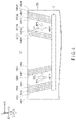
- FIG. 1 is an illustration showing the configuration and the equivalent circuit of a display device of the present embodiment.
- FIG. 2 is a cross-sectional view of a display area of a display panel shown in FIG. 1 .
- FIG. 3 is a plan view showing a mounting portion of the display panel.
- FIG. 4 is a plan view showing a part of a wiring board.
- FIG. 5 is a plan view showing a state where the wiring board shown in FIG. 4 is mounted on the mounting portion shown in FIG. 3 .
- FIG. 6 is a cross-sectional view of the display device along a signal wiring line and a connection wiring line shown in FIG. 5 .
- FIG. 7 is a cross-sectional view of a process of mounting the wiring board on the display panel.
- FIG. 8 is a plan view showing the wiring board and a suction device shown in FIG. 7 .
- FIG. 9 is a cross-sectional view showing the wiring board and the suction device along line A-B shown in FIG. 8 .
- FIG. 10 is a plan view showing a comparison on the mounting portion between a comparative example and the present embodiment.
- FIG. 11 is a plan view showing a comparison on the width of the non-display area in accordance with a change of the width of the wiring board.
- FIG. 12 is a plan view showing the first modification example of the present embodiment.
- FIG. 13 is a plan view showing the second modification example of the present embodiment.
- a display device comprising: a display panel comprising a first substrate; and a wiring board mounted on a mounting portion of the first substrate.
- the display panel comprises a first terminal and a second terminal located in the mounting portion, a first alignment mark located in the mounting portion and located between the first terminal and the second terminal, a first wiring line connected to the first terminal, and a second wiring line connected to the second terminal.
- the wiring board comprises a first connection wiring line connected to the first terminal, a second connection wiring line connected to the second terminal, and a second alignment mark located between the first connection wiring line and the second connection wiring line.
- a method for manufacturing a display device comprising: a display panel comprising a first substrate; and a wiring board mounted on a mounting portion of the first substrate, wherein the display panel comprises a first terminal and a second terminal located in the mounting portion, a first alignment mark located in the mounting portion and located between the first terminal and the second terminal, a first wiring line connected to the first terminal, and a second wiring line connected to the second terminal, and the wiring board comprises a first connection wiring line connected to the first terminal, a second connection wiring line connected to the second terminal, and a second alignment mark located between the first connection wiring line and the second connection wiring line.
- the method comprises: sucking the wiring substrate by a suction device comprising a first suction port and a second suction port, wherein the suction device sucks the wiring substrate such that the first suction port is positioned overlapping the first connection wiring line, the second suction port is positioned overlapping the second connection wiring line, and both sides of the second alignment mark are sucked; aligning the display panel and the wiring board by the first alignment mark and the second alignment mark; and connecting the first terminal and the first connection wiring line together and the second terminal and the second connection wiring line together by an anisotropic conductive film.
- the main configuration of the present embodiment can be used for an electronic device comprising a flexible wiring board such as a display device.
- a display device can be used for various devices such as a smartphone, a tablet computer, a portable telephone, a notebook computer, an in-car device and a game console.
- the present embodiment can be applied to various display devices such as a liquid crystal display device, a self-luminous display device such as an organic electroluminescent display device, a micro-LED display device, an electronic paper display device comprising an electrophoretic element or the like, a display device employing micro-electromechanical systems (MEMS), and a display device employing electrochromism.
- MEMS micro-electromechanical systems
- the present embodiment can also be applied to a wearable display device or a variant display device.
- FIG. 1 is an illustration showing the configuration and the equivalent circuit of the display device DSP of the present embodiment.
- a first direction X, a second direction Y and a third direction Z are orthogonal to one another. However, they may cross one another at an angle other than 90 degrees.
- the first direction X and the second direction Y correspond to directions parallel to the main surface of a substrate constituting the display device DSP
- the third direction Z corresponds to the thickness direction of the display device DSP.
- a direction toward the point of an arrow indicating the third direction Z is referred to as upward (or simply above), and a direction from the point of the arrow toward the opposite side is referred to as downward (or simply below).
- the display device DSP comprises a display panel PNL and a wiring board WB mounted on the display panel PNL.
- the display panel PNL is a liquid crystal display panel, and comprises a first substrate SUB 1 , a second substrate SUB 2 opposed to the first substrate SUB 1 , a sealing member SE, a liquid crystal layer LC, a signal line S, a scanning line G, a switching element SW, a pixel electrode PE, a common electrode CE and the like.
- the display panel PNL comprises a display area DA which displays an image and a non-display area NDA which surrounds the display area DA.
- the first substrate SUB 1 comprises a mounting portion MA exposed to the outside of the second substrate SUB 2 .
- the sealing member SE is located in the non-display area NDA and bonds the first substrate SUB 1 and the second substrate SUB 2 together.
- an area in which the sealing member SE is disposed is indicated by upward-sloping hatch lines.
- the display area DA is located inside surrounded by the sealing member SE.
- the display panel PNL comprises a plurality of pixels PX disposed in a matrix in the first direction X and the second direction Y in the display area DA.
- the signal line S, the scanning line G, the switching element SW, the pixel electrode PE, the common electrode CE and the liquid crystal layer LC are located in the display area DA.
- the signal line S extends along the second direction Y, and the scanning line G extends along the first direction X.
- the switching element SW is composed of, for example, a thin-film transistor (TFT), and is electrically connected to the scanning line G and the signal line S.
- the pixel electrode PE is electrically connected to the switching element SW.
- Each pixel electrode PE is opposed to the common electrode CE, and drives the liquid crystal layer LC by an electric field produced between the pixel electrode PE and the common electrode CE.
- a storage capacitance CS is formed, for example, between an electrode of the same potential as the common electrode CE and an electrode of the same potential as the pixel electrode PE.
- the flexible wiring board WB is mounted on the mounting portion MA.
- the wiring board WB comprises a driver IC chip 2 which drives the display panel PNL.
- the driver IC chip 2 may be mounted on the mounting portion MA.
- the display panel PNL of the present embodiment may be any one of a transmissive type comprising a transmissive display function of displaying an image by selectively transmitting light from the rear side of the first substrate SUB 1 , a reflective type comprising a reflective display function of displaying an image by selectively reflecting light from the front side of the second substrate SUB 2 , and a transflective type comprising the transmissive display function and the reflective display function.
- the display panel PNL may comprise a configuration corresponding to any one of a display mode using a lateral electric field along the main surface of a substrate, a display mode using a longitudinal electric field along a normal to the main surface of a substrate, a display mode using an inclined electric field inclined in an oblique direction with respect to the main surface of a substrate, and a display mode using an arbitrary combination of the lateral electric field, the longitudinal electric field and the inclined electric field.
- the main surface of a substrate here is a surface parallel to an XY-plane defined by the first direction X and the second direction Y.
- FIG. 2 is a cross-sectional view of the display area DA of the display panel PNL shown in FIG. 1 .
- the illustrated example corresponds to an example where the display mode using the lateral electric field is applied to the display panel PNL.
- the display device DSP comprises a first optical element OD 1 , a second optical element OD 2 and an illumination device IL in addition to the display panel PNL.
- the first substrate SUB 1 comprises an insulating substrate 10 , insulating films 11 to 16 , signal lines S 1 and S 2 , metal wiring lines ML 1 and ML 2 , the common electrode CE, the pixel electrode PE, and an alignment film AL 1 .
- the insulating substrate 10 is a substrate having optical transparency such as a glass substrate or a flexible resin substrate.
- the insulating film 11 is located on the insulating substrate 10 .
- the insulating film 12 is located on the insulating film 11 .
- the insulating film 13 is located on the insulating film 12 .
- the signal lines S 1 and S 2 are located on the insulating film 13 , and are covered with the insulating film 14 .
- the metal wiring lines ML 1 and ML 2 are located on the insulating film 14 , and are covered with the insulating film 15 .
- the metal wiring lines ML 1 and ML 2 are located directly above the signal lines S 1 and S 2 , respectively.
- the common electrode CE is located on the insulating film 15 , and is covered with the insulating film 16 .
- the pixel electrode PE is located on the insulating film 16 , and is covered with the alignment film AL 1 .
- the common electrode CE and the pixel electrode PE are transparent electrodes formed of a transparent conductive material such as indium tin oxide (ITO) or indium zinc oxide (IZO).
- the insulating films 11 to 13 and the insulating film 16 are inorganic insulating films formed of an inorganic insulating material such as silicon oxide, silicon nitride or silicon oxynitride, and may have a single-layer structure or a multilayer structure.
- the insulating films 14 and 15 are organic insulating films formed of an organic insulating material such as acrylic resin, for example.
- the second substrate SUB 2 comprises an insulating substrate 20 , a light-shielding layer BM, a color filter CF, an overcoat layer OC, an alignment film AL 2 and the like.
- the insulating substrate 20 is a substrate having optical transparency such as a glass substrate or a resin substrate.
- the light-shielding layer BM and the color filter CF are located on a side of the insulating substrate 20 which is opposed to the first substrate SUB 1 .
- the color filter CF is disposed at a position opposed to the pixel electrode PE, and partially overlaps the light-shielding layer BM.
- the color filter CF comprises a red color filter CFR, a green color filter CFG and a blue color filter CFB.
- the overcoat layer OC covers the color filter CF.
- the overcoat layer OC is formed of transparent resin.
- the alignment film AL 2 covers the overcoat layer OC.
- the alignment film AL 1 and the alignment film AL 2 are formed of, for example, a material exhibiting horizontal alignment properties.
- the first substrate SUB 1 and the second substrate SUB 2 are disposed such that the alignment film AL 1 and the alignment film AL 2 are opposed to each other.
- the first substrate SUB 1 and the second substrate SUB 2 are bonded by the sealing member with a predetermined cell gap in between.
- the liquid crystal layer LC is held between the alignment film AL 1 and the alignment film AL 2 .
- the liquid crystal layer LC comprises liquid crystal molecules LM.
- the liquid crystal layer LC is composed of a positive liquid crystal material (whose dielectric anisotropy is positive) or a negative liquid crystal material (whose dielectric anisotropy is negative).
- the first optical element OD 1 including a polarizer PL 1 is bonded to the insulating substrate 10 .
- the second optical element OD 2 including a polarizer PL 2 is bonded to the insulating substrate 20 .
- the first optical element OD 1 and the second optical element OD 2 may each comprise a retarder, a scattering layer, an antireflective layer and the like as needed.
- the liquid crystal molecules LM are initially aligned in a predetermined direction between the alignment film AL 1 and the alignment film AL 2 .
- the liquid crystal molecules LM are aligned in a direction different from the initial alignment direction by an electric field, and the alignment direction is controlled by the electric field. In this on state, a part of the light from the illumination device IL is transmitted through the first optical element OD 1 and the second optical element OD 2 , and light display is realized.
- FIG. 3 is a plan view showing the mounting portion MA of the display panel PNL.
- a direction crossing at an acute angle counterclockwise with respect to the second direction Y is defined as a direction D 1
- a direction crossing at an acute angle clockwise with respect to the second direction Y is defined as a direction D 2 .
- An angle ⁇ 1 between the second direction Y and the direction D 1 is substantially equal to an angle ⁇ 2 between the second direction Y and the direction D 2 .
- the display panel PNL comprises terminals PD 1 to PD 9 located in the mounting portion MA, terminals PD 21 to PD 29 , alignment marks AM 11 and AM 12 located in the mounting portion MA, signal wiring lines SW 1 to SW 9 connected respectively to the terminals PD 1 and PD 9 , and signal wiring lines SW 21 to SW 29 connected respectively to the terminals PD 21 to PD 29 .
- the signal wiring lines SW can also be referred to simply as wiring lines SW
- wiring lines drawn from the terminals PD of the mounting portion MA may be wiring lines which supply a signal for driving the display panel PNL from the driver IC chip, and each are a power supply line or a wiring line which supplies a voltage of a fixed potential or the like.
- the wiring lines SW 1 to SW 5 are power supply lines which supply various voltages to the display panel PNL
- the wiring lines SW 6 to SW 9 are signal wiring lines which supply various signals to the display panel PNL.
- Wiring lines clustered across the alignment mark AM which will be described later can be grouped according to a purpose or a function.
- the alignment mark AM 11 is located between the terminal PD 5 and the terminal PD 6 .
- the alignment mark AM 12 is located between the terminal PD 24 and the terminal PD 25 .
- the terminals PD 1 to PD 5 , the alignment mark AM 11 and the terminals PD 6 to PD 9 are arranged in parallel in this order in the first direction X.
- the terminals PD 21 to PD 24 , the alignment mark AM 12 and the terminals PD 25 to PD 29 are arranged in parallel in this order in the first direction X.
- the alignment mark AM 11 comprises an island portion I 1 , an island portion I 2 arranged in parallel in the first direction X of the island portion I 1 , an island portion I 3 arranged in parallel in the second direction Y of the island portion I 1 , and an island portion I 4 arranged in parallel in the second direction Y of the island portion I 2 .
- the alignment mark AM 12 comprises an island portion I 5 , an island portion I 6 arranged in parallel in the first direction X of the island portion I 5 , an island portion I 7 arranged in parallel in the second direction Y of the island portion I 5 , and an island portion I 8 arranged in parallel in the second direction Y of the island portion I 6 .
- the island portions I 1 to I 8 are formed in, for example, a rectangular shape. However, they are not limited to a rectangular shape but may be formed in any shape as long as they have a function as an alignment mark.
- the center position of the width along the first direction X of the mounting portion MA is defined as a center line L 1 .
- the center line L 1 is parallel to the second direction Y.
- the terminals PD 1 to PD 9 , the signal wiring lines SW 1 to SW 9 , and the alignment mark AM 11 are located on the left side of the center line L 1 .
- the terminals PD 21 to PD 29 , the signal wiring lines SW 21 to SW 29 , and the alignment mark AM 12 are located on the right side of the center line L 1 .
- the alignment marks AM 11 and AM 12 are disposed at positions substantially symmetric with respect to the center line L 1 .
- the signal wiring lines SW 1 to SW 9 extend along the direction D 1 .
- the signal wiring lines SW 21 to SW 29 extend along the direction D 2 .
- FIG. 4 is a plan view showing a part of the wiring board WB.
- the wiring board WB comprises connection wiring lines WR 1 to WR 9 , connection wiring lines WR 21 to WR 29 , and alignment marks AM 21 and AM 22 .
- the connection wiring lines WR 1 to WR 9 and the connection wiring lines WR 21 to WR 29 are connected to the driver IC chip 2 .
- the connection wiring lines WR can also be referred to simply as wiring lines WR but are referred to as connection wiring lines in the present specification simply because the wiring lines WR of the wiring board WB are connected to the display panel PNL.
- the alignment mark AM 21 is located between the connection wiring line WR 5 and the connection wiring line WR 6 .
- the alignment mark AM 22 is located between the connection wiring line WR 24 and the connection wiring line WR 25 .
- the connection wiring lines WR 1 to WR 5 , the alignment mark AM 21 , and the connection wiring lines WR 6 to WR 9 are arranged in parallel in this order in the first direction X.
- the connection wiring lines WR 21 to WR 24 , the alignment mark AM 22 , and the connection wiring lines WR 25 to WR 29 are arranged in parallel in this order in the first direction X.
- the alignment mark AM 21 is formed in a cross shape comprising an extension portion EP 1 extending in the first direction X and an extension portion EP 2 extending in the second direction Y.
- the alignment mark AM 22 is formed in a cross shape comprising an extension portion EP 3 extending in the first direction X and an extension portion EP 4 extending in the second direction Y.
- the alignment marks of the wiring board WB are not limited to a cross shape but may be formed in any shape as long as they have a function as an alignment mark.
- the center position of the width in the first direction X of the wiring board WB is defined as a center line L 2 .
- the center line L 2 is parallel to the second direction Y.
- the connection wiring lines WR 1 to WR 9 and the alignment mark AM 21 are located on the left side of the center line L 2 .
- the connection wiring lines WR 21 to WR 29 and the alignment mark AM 22 are located on the right side of the center line L 2 .
- the alignment marks AM 21 and AM 22 are disposed at positions substantially symmetric with respect to the center line L 2 .
- the connection wiring lines WR 1 to WR 9 extend along the direction D 1 .
- the connection wiring lines WR 21 to WR 29 extend along the direction D 2 .
- connection wiring lines WR 1 to WR 9 and WR 21 to WR 29 , and the alignment marks AM 21 to AM 22 are formed of, for example, a metal film such as copper, and the surface of the metal film is plated with tin or the like.
- FIG. 5 is a plan view showing a state where the wiring board WB shown in FIG. 4 is mounted on the mounting portion MA shown in FIG. 3 .
- connection wiring lines WR 1 to WR 9 of the wiring board WB are connected to the terminals PD 1 to PD 9 of the mounting portion MA, respectively.
- connection wiring lines WR 21 to WR 29 of the wiring board WB are connected to the terminals PD 21 to PD 29 of the mounting portion MA, respectively.
- the alignment marks AM 11 and AM 21 are arranged in parallel in the second direction Y.
- the alignment marks AM 12 and AM 22 are arranged in parallel in the second direction Y.
- the signal wiring lines SW 1 to SW 9 and the connection wiring lines WR 1 to WR 9 located on the left side of the center line L 1 extend along the direction D 1 . Therefore, a center point O 11 of the alignment mark AM 11 and a center point O 21 of the alignment mark AM 21 are arranged in parallel along the direction D 1 . That is, the center point O 21 is located on the center line L 1 side of the center point O 11 .
- the island portions I 2 and I 4 and the extension portion EP 2 are arranged in the second direction Y.
- the signal wiring lines SW 21 to SW 29 and the connection wiring lines WR 21 to WR 29 located on the right side of the center line L 1 extend along the direction D 2 . Therefore, a center point O 12 of the alignment mark AM 12 and a center point O 22 of the alignment mark AM 22 are arranged in parallel along the direction D 2 . That is, the center point O 22 is located on the center line L 1 side of the center point O 12 .
- the island portions I 5 and I 7 and the extension portion EP 4 are arranged in the second direction Y.
- the alignment marks are used for aligning the display panel PNL and the wiring board WB when they are connected together. They are aligned when the positions of the alignment marks of them reach predetermined values.
- the number of signal wiring lines and the number of connection wiring lines disposed on the right side and the left side of the alignment marks are not limited. Only at least one set of a signal wiring line and a connection wiring line has to be positioned on the left side of the alignment marks AM 11 and AM 21 . Similarly, only at least one set of a signal wiring line and a connection wiring line has to be positioned on the right side of the alignment marks AM 12 and AM 22 . Furthermore, in the illustrated example, the center point of the alignment mark of the display panel PNL and the center point of the alignment mark of the wiring board WB are offset from each other. However, the center point O 11 of the alignment mark AM 11 and the center point O 21 of the alignment mark AM 21 may overlap each other, and the center point O 12 of the alignment mark AM 12 and the center point O 22 of the alignment mark AM 22 may overlap each other.
- FIG. 6 is a cross-sectional view of the display device DSP along the signal wiring line SW 1 and the connection wiring line WR 1 shown in FIG. 5 . That is, FIG. 6 is a plan view along a plane defined by the third direction Z and the direction D 1 .
- the signal wiring line SW 1 is located between the insulating film 12 and the insulating film 13 .
- the signal wiring line SW 1 is located in the same layer as the scanning line G shown in FIG. 1 and is formed of the same material as the scanning line G.
- the signal wiring line SW 1 and the scanning line G are formed of a metal material such as aluminum (Al), titanium (Ti), silver (Ag), molybdenum (Mo), tungsten (W), copper (Cu) or chromium (Cr), an alloy of these metal materials combined together or the like, and may have a single-layer structure or a multilayer structure.
- the signal wiring line SW 1 and the scanning line G are formed of a molybdenum tungsten alloy.
- the alignment marks AM 11 and AM 12 shown in FIG. 5 are located in the same layer as the signal wiring line SW 1 , and are formed of the same material as the signal wiring line SW 1 and the scanning line G.
- the terminal PD 1 is composed of metal layers MEL 1 and MEL 2 and transparent conductive layers TL 1 and TL 2 .
- the metal layer MEL 1 is located between the insulating film 13 and the insulating film 14 , and is in contact with the signal wiring line SW 1 via a contact hole of the insulating film 13 .
- the metal layer MEL 1 is located in the same layer and formed of the same material as the signal lines S 1 and S 2 shown in FIG. 2 .
- the metal layer MEL 1 and the signal lines S 1 and S 2 are formed of any one of the above-described metal materials, an alloy of the above-described metal materials combined together or the like, and may have a single-layer structure or a multilayer structure.
- the metal layer MEL 1 and the signal lines S 1 and S 2 are formed of a layer stack of the first layer containing titanium (Ti), the second layer containing aluminum (Al) and the third layer containing titanium (Ti) stacked in this order.
- the metal layer MEL 2 is located between the insulating film 14 and the insulating film 15 , and is in contact with the metal layer MEL 1 via a contact hole of the insulating film 14 .
- the metal layer MEL 2 is located in the same layer and formed of the same material as the metal wiring lines ML 1 and ML 2 shown in FIG. 2 .
- the metal layer MEL 2 and the metal wiring lines ML 1 and ML 2 are formed of any one of the above-described metal materials, an alloy of the above-described metal materials combined together or the like, and may have a single-layer structure or a multilayer structure.
- the metal layers MEL 2 and the metal wiring lines ML 1 and ML 2 each are a layer stack of the first layer containing titanium (Ti), the second layer containing aluminum (Al) and the third layer containing titanium (Ti) stacked in this order, or a layer stack of the first layer containing molybdenum (Mo), the second layer containing aluminum (Al) and the third layer containing molybdenum (Mo) stacked in this order.
- the transparent conductive layer TL 1 is located between the insulating film 15 and the insulating film 16 , and is in contact with the metal layer MEL 2 via a contact hole of the insulating film 15 .
- the transparent conductive layer TL 1 is located in the same layer and formed of the same material as the common electrode CE shown in FIG. 2 .
- the transparent conductive film TL 2 is located on the insulating film 16 and is in contact with the transparent conductive film TL 1 via a contact hole of the insulating film 16 .
- the transparent conductive film TL 2 is located in the same layer and formed of the same material as the pixel electrode PE shown in FIG. 2 .
- the wiring board WB comprises an insulating substrate 30 , the connection wiring line WR 1 , and a solder resist SR covering the connection wiring line WR 1 .
- the insulating substrate 30 comprises an upper surface 30 a and a lower surface 30 b .
- the insulating substrate 30 is formed of, for example, polyimide.
- the connection wiring line WR 1 is located on the lower surface 30 b of the insulating substrate 30 .
- the solder resistor SR does not extend to a position opposed to the terminal PD 1 of the display panel PNL but exposes the connection wiring line WR 1 at the position opposed to the terminal PD 1 .
- the wiring board WB is electrically connected and bonded to the display panel PNL by an anisotropic conductive film 3 which is a conductive material.
- the anisotropic conductive film 3 is interposed between the first substrate SUB 1 and the wiring board WB.
- the wiring board WB and the display panel PNL are electrically and physically connected together by pressing them from above and below in the third direction Z with the anisotropic conductive film 3 interposed and heating them.
- the anisotropic conductive film 3 connects the terminals PD 1 to PD 5 and the connection wiring lines WR 1 to WR 5 , the terminals PD 6 to PD 9 and the connection wiring lines WR 6 to WR 9 , the terminals PD 21 to PD 24 and the connection wiring lines WR 21 to WR 24 , and the terminals PD 25 to PD 29 and the connection wiring lines WR 25 to WR 29 shown in FIG. 5 .
- FIG. 7 is a cross-sectional view showing a process of mounting the wiring board WB on the display panel PNL.
- the display panel PNL is disposed on a stage ST. As shown in FIGS. 8 and 9 , the wiring board WB is attracted to a suction device 100 .
- the suction device 100 comprises a space inside, and turns the space into a vacuum and attracts the wiring board WB.
- the suction device 100 attracts the upper surface 30 a of the insulating substrate 30 .
- the alignment mark AM 21 of the wiring board WB is located on the lower surface 30 b side of the insulating substrate 30 .
- the mounting of the wiring board WB on the display panel PNL takes the following procedure.
- Light LT is emitted from below the display panel PNL, and an image is captured from below the display panel PNL by a camera for recognizing the alignment marks.
- a manufacturing device recognizes the position of the alignment mark of the display panel PNL and the position of the alignment mark of the wiring board WB, and aligns the display panel PNL and the wiring board WB. Then, the display panel PNL and the wiring board WB are bonded with the anisotropic conductive film interposed by thermocompression bonding.
- FIG. 8 is a plan view showing the wiring board WB and the suction device 100 shown in FIG. 7 .
- FIG. 8 is a plan view from above the suction device 100 shown in FIG. 7 .
- the suction device 100 comprises suction ports SH 1 to SH 4 arranged in the first direction X.
- the suction port SH 1 overlaps the connection wiring lines WR 1 to WR 4
- the suction port SH 2 overlaps the connection wiring lines WR 6 to WR 13
- the suction port SH 3 overlaps the connection wiring lines WR 17 to WR 24
- the suction port SH 4 overlaps the connection wiring line WR 25 to WR 29 .
- the alignment mark AM 21 is located between the suction port SH 1 and the suction port SH 2
- the alignment mark AM 22 is located between the suction port SH 3 and the suction port SH 4 .
- the suction device 100 attracts the wiring board WB such that the suction ports are located on the right side and the left side of the alignment mark.
- the suction device 100 sucks both sides of the alignment mark AM 21 and both sides of the alignment mark AM 22 .
- the suction device 100 comprises suction ports (not shown) also between the suction port SH 2 and the suction port SH 3 .
- the display panel PNL and the wiring board WB are aligned by the alignment marks AM 11 and AM 21 and aligned by the alignment marks AM 12 and AM 22 as shown in FIG. 5 . At this time, the alignment marks AM 11 and AM 21 do not overlap each other, and the alignment marks AM 12 and AM 22 do not overlap each other.
- FIG. 9 is a cross-sectional view showing the wiring board WB and the suction device 100 along line A-B shown in FIG. 8 .
- the suction device 100 comprises a space SP inside.
- the space SP communicates with the suction ports SH 1 to SH 4 .
- the suction ports SH 1 to SH 4 are hermetically closed by the upper surface 30 a of the insulating substrate 30 .
- the wiring board WB tends to roll up under no external force. Since the suction ports SH 1 and SH 2 attract areas on the right side and the left side of the alignment mark AM 21 , a part of the wiring board WB in which the alignment mark AM 21 is located can be maintained flat. Similarly, since the suction ports SH 3 and SH 4 attract areas on the right side and the left side of the alignment marks AM 22 , a part of the wiring board WB in which the alignment mark AM 22 is located can be maintained flat.
- FIG. 10 is a plan view showing a comparison on the positions of the alignment marks AM 11 and AM 12 between a comparative example and the present embodiment.
- FIG. 10 ( a ) is a plan view showing the comparative example
- FIG. 10 ( b ) is a plan view showing the present embodiment.
- the configuration on the left side of the center line L 1 is illustrated. Since the configuration on the right side of the center line L 1 is similar to this configuration, description will be omitted.
- the alignment marks AM 11 and AM 2 l are located more outward than the signal wiring line SW 1 and the connection wiring line WR 1 .
- the suction area AR corresponds to an area indicated by hatch lines in the drawing.
- the width in the first direction X of the suction area AR is about greater than or equal to 0.65 mm.
- the alignment marks AM 11 and AM 21 are located between the signal wiring line SW 5 and the connection wiring line WR 5 and the signal wiring line SW 6 and the connection wiring line WR 6 . Therefore, the suction area AR overlaps the connection wiring lines WR 1 to WR 5 . That is, the suction area AR and the area for disposing the connection wiring lines WR 1 to WR 5 can be combined. Therefore, the distance from the center line L 1 to an edge portion EG of the wiring board WB can be reduced as compared with the comparative example. For example, the distance from the edge portion EG of the wiring board WB to the center line L 1 can be reduced by about 0.35 mm as compared with the comparative example.
- the width in the first direction X of the suction area AR is about greater than or equal to about 0.65 mm. As described above, it is possible to reduce the width of the wiring board WB without reducing the suction area AR. Furthermore, since the width of the wiring substrate WB can be reduced, the wiring board WB fit for the miniaturization of the display panel PNL can be manufactured.
- connection wiring line WR 1 can be located close to the edge portion EG, and the area for disposing the connection wiring lines WR can be increased. Therefore, the number of connection wiring lines WR can be increased or the pitch of the connection wiring lines WR can be increased. Furthermore, when the pitch is increased, the width of the connection wiring lines WR can be increased, and the resistance can be reduced. When the number, the pitch and the width of the connection wiring lines WR are increased, the number, the pitch and the width of the signal wiring lines SW of the display panel PNL can be increased, accordingly. Furthermore, when the pitch and the width of the signal wiring lines SW and the pitch and the width of the connection wiring lines WR are increased, the risk of the misalignment of the display panel PNL and the wiring board WB can be reduced. Note that it is also possible to increase the area for disposing the connection wiring lines WR without reducing the width of the wiring board WB.
- FIG. 11 is a plan view showing a comparison on the mounting portion MA between a comparative example and the present embodiment.
- FIG. 11 ( a ) is a plan view showing the comparative example
- FIG. 11 ( b ) is a plan view showing the present embodiment.
- the display device DSP comprises barcodes BC 1 and BC 2 located in the mounting portion MA and test terminals TT 1 and TT 2 located in the mounting portion MA.
- the barcode BC 1 and the test terminal TT 1 are arranged in the second direction Y on the left side of the wiring board WB
- the barcode BC 2 and the test terminal TT 2 are arranged in the second direction Y on the right side of the wiring board WB.
- the wiring board WB has a width W 11 in the first direction X.
- the mounting portion MA has a width W 1 in the second direction Y.
- the wiring board WB has a width W 12 in the first direction X, and the width W 12 is less than the width W 11 . Therefore, areas on the right side and the left side of the wiring board WB can be expanded as compared with the comparative example. That is, the barcode BC 1 and the test terminal TT 1 can be arranged in the first direction X on the left side of the wiring board WB, and the barcode BC 2 and the test terminal TT 2 can be arranged in the first direction X on the right side of the wiring board WB. Therefore, the width W 2 in the second direction Y of the mounting portion MA can be made less than the width W 1 of the comparative example.
- the barcode and the test terminal are taken as an example. However, the elements are not limited to them but may be other members.
- the curvatures of corner portions CN 1 and CN 2 of the display panel PNL can be expanded. That is, the desired corner portions CN 1 and CN 2 according to the requested shape of the display device can be formed. Furthermore, since the connection wiring lines WR of the wiring board WB can be located more outward, an area for drawing signal wiring lines to be connected can be reduced, and the non-display area NDA on the mounting portion MA side can be reduced.
- FIG. 12 is a plan view showing the first modification example of the present embodiment.
- the configuration shown in FIG. 12 is different from the configuration shown in FIG. 10 ( b ) in that dummy terminals DM 1 to DM 10 are disposed.
- the wiring board WB comprises dummy terminals DM 1 to DM 5 overlapping the alignment mark AM 11 , and dummy terminals DM 6 to DM 10 located on an opposite side to the dummy terminals DM 1 to DM 5 with respect to the alignment mark AM 21 .
- the dummy terminals DM 1 to DM 10 are located between the connection wiring line WR 5 and the connection wiring line WR 6 and extend along the direction D 1 .
- the dummy terminals DM 6 to DM 10 do not overlap the alignment mark AM 11 .
- FIG. 13 is a plan view showing the second modification example of the present embodiment.
- the configuration of FIG. 13 is different from the configuration shown in FIG. 10 ( b ) in that the signal wiring lines SW 1 to SW 9 , the terminals PD 1 to PD 9 , and the connection wiring lines WR 1 to WR 9 extend along the second direction Y.
- the center point O 11 of the alignment mark AM 11 and the center point O 21 of the alignment mark AM 21 are arranged in parallel along the second direction Y.
- the alignment mark AM 11 comprises a gap GP along the second direction Y between the island portions I 1 and I 3 and the island portions I 2 and I 4 .
- the gap GP and the extension portion EP 2 of the alignment mark AM 21 are arranged in the second direction Y.
- a display device, a display panel and a wiring board which can achieve miniaturization can be obtained.
Landscapes
- Physics & Mathematics (AREA)
- Engineering & Computer Science (AREA)
- Nonlinear Science (AREA)
- General Physics & Mathematics (AREA)
- Microelectronics & Electronic Packaging (AREA)
- Mathematical Physics (AREA)
- Chemical & Material Sciences (AREA)
- Crystallography & Structural Chemistry (AREA)
- Optics & Photonics (AREA)
- Theoretical Computer Science (AREA)
- Devices For Indicating Variable Information By Combining Individual Elements (AREA)
- Liquid Crystal (AREA)
- Computer Hardware Design (AREA)
- Power Engineering (AREA)
- Condensed Matter Physics & Semiconductors (AREA)
- Combinations Of Printed Boards (AREA)
Abstract
Description
Claims (6)
Applications Claiming Priority (4)
| Application Number | Priority Date | Filing Date | Title |
|---|---|---|---|
| JP2018178968A JP7123718B2 (en) | 2018-09-25 | 2018-09-25 | DISPLAY DEVICE AND METHOD FOR MANUFACTURING DISPLAY DEVICE |
| JP2018-178968 | 2018-09-25 | ||
| JPJP2018-178968 | 2018-09-25 | ||
| PCT/JP2019/037377 WO2020067062A1 (en) | 2018-09-25 | 2019-09-24 | Display device and method for manufacturing display device |
Related Parent Applications (1)
| Application Number | Title | Priority Date | Filing Date |
|---|---|---|---|
| PCT/JP2019/037377 Continuation WO2020067062A1 (en) | 2018-09-25 | 2019-09-24 | Display device and method for manufacturing display device |
Publications (2)
| Publication Number | Publication Date |
|---|---|
| US20210223597A1 US20210223597A1 (en) | 2021-07-22 |
| US11487170B2 true US11487170B2 (en) | 2022-11-01 |
Family
ID=69951941
Family Applications (1)
| Application Number | Title | Priority Date | Filing Date |
|---|---|---|---|
| US17/205,101 Active US11487170B2 (en) | 2018-09-25 | 2021-03-18 | Display device and method for manufacturing display device |
Country Status (3)
| Country | Link |
|---|---|
| US (1) | US11487170B2 (en) |
| JP (1) | JP7123718B2 (en) |
| WO (1) | WO2020067062A1 (en) |
Families Citing this family (2)
| Publication number | Priority date | Publication date | Assignee | Title |
|---|---|---|---|---|
| CN109742050B (en) * | 2019-01-03 | 2022-02-01 | 京东方科技集团股份有限公司 | Substrate and alignment method and equipment |
| KR20220014405A (en) * | 2020-07-24 | 2022-02-07 | 삼성디스플레이 주식회사 | Display apparatus |
Citations (11)
| Publication number | Priority date | Publication date | Assignee | Title |
|---|---|---|---|---|
| JPH07329914A (en) | 1994-06-06 | 1995-12-19 | Sharp Corp | Tape carrier package alignment mounting method and tape carrier package mounting device |
| JP2002122877A (en) | 2000-10-13 | 2002-04-26 | Hitachi Ltd | Liquid crystal display |
| US20030053056A1 (en) | 2001-09-14 | 2003-03-20 | Tohoku Pioneer Corporation | Mark for visual inspection upon assembling a display |
| JP2003131584A (en) | 2001-10-24 | 2003-05-09 | Seiko Epson Corp | Liquid crystal display panel and manufacturing method thereof, liquid crystal display device, and electronic device |
| CN1632648A (en) | 2004-12-29 | 2005-06-29 | 友达光电股份有限公司 | Identification chip for glass substrate and manufacturing method thereof |
| US20070275578A1 (en) | 2006-05-29 | 2007-11-29 | Epson Imaging Devices Corporation | Wiring board, mount structure, and method for manufacturing the same |
| US20170184903A1 (en) * | 2015-12-28 | 2017-06-29 | Seiko Epson Corporation | Electrooptic device and electronic device |
| US20170357122A1 (en) * | 2016-06-08 | 2017-12-14 | Samsung Display Co., Ltd. | Display apparatus and method of manufacturing the same |
| US20180032190A1 (en) * | 2016-07-29 | 2018-02-01 | Japan Display Inc. | Display device |
| US20190116662A1 (en) * | 2016-05-24 | 2019-04-18 | Boe Technology Group Co., Ltd. | Circuit board structure, binding test method and display device |
| US20190116672A1 (en) * | 2017-10-17 | 2019-04-18 | Boe Technology Group Co., Ltd. | Display panel, detection method thereof, flexible printed circuit and display device |
Family Cites Families (2)
| Publication number | Priority date | Publication date | Assignee | Title |
|---|---|---|---|---|
| JP2002258767A (en) | 2001-02-28 | 2002-09-11 | Toshiba Corp | Flat display device, manufacturing method thereof, and printed wiring board used therefor |
| JP2016075896A (en) | 2014-10-07 | 2016-05-12 | 凸版印刷株式会社 | Display panel and manufacturing method thereof |
-
2018
- 2018-09-25 JP JP2018178968A patent/JP7123718B2/en active Active
-
2019
- 2019-09-24 WO PCT/JP2019/037377 patent/WO2020067062A1/en not_active Ceased
-
2021
- 2021-03-18 US US17/205,101 patent/US11487170B2/en active Active
Patent Citations (13)
| Publication number | Priority date | Publication date | Assignee | Title |
|---|---|---|---|---|
| JPH07329914A (en) | 1994-06-06 | 1995-12-19 | Sharp Corp | Tape carrier package alignment mounting method and tape carrier package mounting device |
| JP2002122877A (en) | 2000-10-13 | 2002-04-26 | Hitachi Ltd | Liquid crystal display |
| US20030053056A1 (en) | 2001-09-14 | 2003-03-20 | Tohoku Pioneer Corporation | Mark for visual inspection upon assembling a display |
| JP2003086999A (en) | 2001-09-14 | 2003-03-20 | Tohoku Pioneer Corp | Visual inspection mark and electronic apparatus |
| JP2003131584A (en) | 2001-10-24 | 2003-05-09 | Seiko Epson Corp | Liquid crystal display panel and manufacturing method thereof, liquid crystal display device, and electronic device |
| CN1632648A (en) | 2004-12-29 | 2005-06-29 | 友达光电股份有限公司 | Identification chip for glass substrate and manufacturing method thereof |
| US20070275578A1 (en) | 2006-05-29 | 2007-11-29 | Epson Imaging Devices Corporation | Wiring board, mount structure, and method for manufacturing the same |
| JP2008010829A (en) | 2006-05-29 | 2008-01-17 | Epson Imaging Devices Corp | Wiring board, mounting structure, and manufacturing method thereof |
| US20170184903A1 (en) * | 2015-12-28 | 2017-06-29 | Seiko Epson Corporation | Electrooptic device and electronic device |
| US20190116662A1 (en) * | 2016-05-24 | 2019-04-18 | Boe Technology Group Co., Ltd. | Circuit board structure, binding test method and display device |
| US20170357122A1 (en) * | 2016-06-08 | 2017-12-14 | Samsung Display Co., Ltd. | Display apparatus and method of manufacturing the same |
| US20180032190A1 (en) * | 2016-07-29 | 2018-02-01 | Japan Display Inc. | Display device |
| US20190116672A1 (en) * | 2017-10-17 | 2019-04-18 | Boe Technology Group Co., Ltd. | Display panel, detection method thereof, flexible printed circuit and display device |
Non-Patent Citations (2)
| Title |
|---|
| International Search Report dated Nov. 26, 2019 in PCT/JP2019/037377 filed on Sep. 24, 2019, 2 pages. |
| Office Action dated May 10, 2022, in corresponding Japanese Patent Application No. 2018-178968 (English Translation only), 6 pages. |
Also Published As
| Publication number | Publication date |
|---|---|
| US20210223597A1 (en) | 2021-07-22 |
| JP2020052125A (en) | 2020-04-02 |
| WO2020067062A1 (en) | 2020-04-02 |
| JP7123718B2 (en) | 2022-08-23 |
Similar Documents
| Publication | Publication Date | Title |
|---|---|---|
| US11335739B2 (en) | Display panel and display device | |
| US20200271977A1 (en) | Liquid crystal display substrate and display device | |
| US8823668B2 (en) | Liquid crystal device | |
| TWI402585B (en) | Flexible printed circuit film mother board having a cut pattern and display device provided with a flexible printed circuit film cut by the mother board | |
| CN112424678A (en) | Display device with higher screen ratio | |
| US11508936B2 (en) | Display device including block patterns | |
| US11681186B2 (en) | Display device | |
| CN106980198B (en) | Display device with sensor | |
| US12245457B2 (en) | Display device layer aligned with display panel and display device having the same | |
| US20220231110A1 (en) | Display device | |
| US10925155B2 (en) | Printed circuit board and display device including the same | |
| US11487170B2 (en) | Display device and method for manufacturing display device | |
| US20240219787A1 (en) | Display device and semiconductor substrate | |
| US11340503B2 (en) | Display device | |
| US20190025659A1 (en) | Display device | |
| US11307694B2 (en) | Display device | |
| US20230280518A1 (en) | Display device | |
| US11934075B2 (en) | Display device | |
| WO2018192370A1 (en) | Display device, electronic equipment, and display device manufacturing method | |
| US11249354B2 (en) | Display device and inter-substrate conducting structure | |
| CN119165977A (en) | Display device | |
| JP2021043420A (en) | Display | |
| JP2003156758A (en) | Liquid crystal display device and portable terminal or display device provided with the liquid crystal display device |
Legal Events
| Date | Code | Title | Description |
|---|---|---|---|
| AS | Assignment |
Owner name: JAPAN DISPLAY INC., JAPAN Free format text: ASSIGNMENT OF ASSIGNORS INTEREST;ASSIGNOR:NAKANO, YASUSHI;REEL/FRAME:055634/0770 Effective date: 20210302 |
|
| FEPP | Fee payment procedure |
Free format text: ENTITY STATUS SET TO UNDISCOUNTED (ORIGINAL EVENT CODE: BIG.); ENTITY STATUS OF PATENT OWNER: LARGE ENTITY |
|
| STPP | Information on status: patent application and granting procedure in general |
Free format text: APPLICATION DISPATCHED FROM PREEXAM, NOT YET DOCKETED |
|
| STPP | Information on status: patent application and granting procedure in general |
Free format text: DOCKETED NEW CASE - READY FOR EXAMINATION |
|
| STPP | Information on status: patent application and granting procedure in general |
Free format text: NON FINAL ACTION MAILED |
|
| STPP | Information on status: patent application and granting procedure in general |
Free format text: NON FINAL ACTION MAILED |
|
| STPP | Information on status: patent application and granting procedure in general |
Free format text: RESPONSE TO NON-FINAL OFFICE ACTION ENTERED AND FORWARDED TO EXAMINER |
|
| STPP | Information on status: patent application and granting procedure in general |
Free format text: NOTICE OF ALLOWANCE MAILED -- APPLICATION RECEIVED IN OFFICE OF PUBLICATIONS |
|
| STPP | Information on status: patent application and granting procedure in general |
Free format text: PUBLICATIONS -- ISSUE FEE PAYMENT VERIFIED |
|
| STCF | Information on status: patent grant |
Free format text: PATENTED CASE |
|
| AS | Assignment |
Owner name: MAGNOLIA WHITE CORPORATION, JAPAN Free format text: ASSIGNMENT OF ASSIGNORS INTEREST;ASSIGNOR:JAPAN DISPLAY INC.;REEL/FRAME:072130/0313 Effective date: 20250625 Owner name: MAGNOLIA WHITE CORPORATION, JAPAN Free format text: ASSIGNMENT OF ASSIGNOR'S INTEREST;ASSIGNOR:JAPAN DISPLAY INC.;REEL/FRAME:072130/0313 Effective date: 20250625 |