US11474547B2 - Apparatus and method of balancing input power from multiple sources - Google Patents
Apparatus and method of balancing input power from multiple sources Download PDFInfo
- Publication number
- US11474547B2 US11474547B2 US16/792,073 US202016792073A US11474547B2 US 11474547 B2 US11474547 B2 US 11474547B2 US 202016792073 A US202016792073 A US 202016792073A US 11474547 B2 US11474547 B2 US 11474547B2
- Authority
- US
- United States
- Prior art keywords
- bridges
- power
- power supply
- supply rail
- phase
- Prior art date
- Legal status (The legal status is an assumption and is not a legal conclusion. Google has not performed a legal analysis and makes no representation as to the accuracy of the status listed.)
- Active, expires
Links
Images


Classifications
-
- H—ELECTRICITY
- H02—GENERATION; CONVERSION OR DISTRIBUTION OF ELECTRIC POWER
- H02M—APPARATUS FOR CONVERSION BETWEEN AC AND AC, BETWEEN AC AND DC, OR BETWEEN DC AND DC, AND FOR USE WITH MAINS OR SIMILAR POWER SUPPLY SYSTEMS; CONVERSION OF DC OR AC INPUT POWER INTO SURGE OUTPUT POWER; CONTROL OR REGULATION THEREOF
- H02M3/00—Conversion of DC power input into DC power output
- H02M3/02—Conversion of DC power input into DC power output without intermediate conversion into AC
- H02M3/04—Conversion of DC power input into DC power output without intermediate conversion into AC by static converters
- H02M3/10—Conversion of DC power input into DC power output without intermediate conversion into AC by static converters using discharge tubes with control electrode or semiconductor devices with control electrode
- H02M3/145—Conversion of DC power input into DC power output without intermediate conversion into AC by static converters using discharge tubes with control electrode or semiconductor devices with control electrode using devices of a triode or transistor type requiring continuous application of a control signal
- H02M3/155—Conversion of DC power input into DC power output without intermediate conversion into AC by static converters using discharge tubes with control electrode or semiconductor devices with control electrode using devices of a triode or transistor type requiring continuous application of a control signal using semiconductor devices only
- H02M3/156—Conversion of DC power input into DC power output without intermediate conversion into AC by static converters using discharge tubes with control electrode or semiconductor devices with control electrode using devices of a triode or transistor type requiring continuous application of a control signal using semiconductor devices only with automatic control of output voltage or current, e.g. switching regulators
- H02M3/158—Conversion of DC power input into DC power output without intermediate conversion into AC by static converters using discharge tubes with control electrode or semiconductor devices with control electrode using devices of a triode or transistor type requiring continuous application of a control signal using semiconductor devices only with automatic control of output voltage or current, e.g. switching regulators including plural semiconductor devices as final control devices for a single load
- H02M3/1584—Conversion of DC power input into DC power output without intermediate conversion into AC by static converters using discharge tubes with control electrode or semiconductor devices with control electrode using devices of a triode or transistor type requiring continuous application of a control signal using semiconductor devices only with automatic control of output voltage or current, e.g. switching regulators including plural semiconductor devices as final control devices for a single load with a plurality of power processing stages connected in parallel
-
- G—PHYSICS
- G05—CONTROLLING; REGULATING
- G05F—SYSTEMS FOR REGULATING ELECTRIC OR MAGNETIC VARIABLES
- G05F1/00—Automatic systems in which deviations of an electric quantity from one or more predetermined values are detected at the output of the system and fed back to a device within the system to restore the detected quantity to its predetermined value or values, i.e. retroactive systems
- G05F1/10—Regulating voltage or current
- G05F1/46—Regulating voltage or current wherein the variable actually regulated by the final control device is DC
- G05F1/56—Regulating voltage or current wherein the variable actually regulated by the final control device is DC using semiconductor devices in series with the load as final control devices
- G05F1/565—Regulating voltage or current wherein the variable actually regulated by the final control device is DC using semiconductor devices in series with the load as final control devices sensing a condition of the system or its load in addition to means responsive to deviations in the output of the system, e.g. current, voltage, power factor
-
- G—PHYSICS
- G05—CONTROLLING; REGULATING
- G05F—SYSTEMS FOR REGULATING ELECTRIC OR MAGNETIC VARIABLES
- G05F1/00—Automatic systems in which deviations of an electric quantity from one or more predetermined values are detected at the output of the system and fed back to a device within the system to restore the detected quantity to its predetermined value or values, i.e. retroactive systems
- G05F1/10—Regulating voltage or current
- G05F1/46—Regulating voltage or current wherein the variable actually regulated by the final control device is DC
- G05F1/56—Regulating voltage or current wherein the variable actually regulated by the final control device is DC using semiconductor devices in series with the load as final control devices
- G05F1/575—Regulating voltage or current wherein the variable actually regulated by the final control device is DC using semiconductor devices in series with the load as final control devices characterised by the feedback circuit
-
- G—PHYSICS
- G06—COMPUTING OR CALCULATING; COUNTING
- G06F—ELECTRIC DIGITAL DATA PROCESSING
- G06F1/00—Details not covered by groups G06F3/00 - G06F13/00 and G06F21/00
- G06F1/26—Power supply means, e.g. regulation thereof
- G06F1/28—Supervision thereof, e.g. detecting power-supply failure by out of limits supervision
-
- H—ELECTRICITY
- H02—GENERATION; CONVERSION OR DISTRIBUTION OF ELECTRIC POWER
- H02J—ELECTRIC POWER NETWORKS; CIRCUIT ARRANGEMENTS OR SYSTEMS FOR SUPPLYING OR DISTRIBUTING ELECTRIC POWER; SYSTEMS FOR STORING ELECTRIC ENERGY
- H02J1/00—Circuit arrangements for DC mains or DC distribution networks
- H02J1/10—Parallel operation of DC sources
- H02J1/106—Parallel operation of DC sources for load balancing, symmetrisation, or sharing
-
- H—ELECTRICITY
- H02—GENERATION; CONVERSION OR DISTRIBUTION OF ELECTRIC POWER
- H02J—ELECTRIC POWER NETWORKS; CIRCUIT ARRANGEMENTS OR SYSTEMS FOR SUPPLYING OR DISTRIBUTING ELECTRIC POWER; SYSTEMS FOR STORING ELECTRIC ENERGY
- H02J1/00—Circuit arrangements for DC mains or DC distribution networks
- H02J1/14—Balancing load and power generation in DC networks
-
- H—ELECTRICITY
- H03—ELECTRONIC CIRCUITRY
- H03M—CODING; DECODING; CODE CONVERSION IN GENERAL
- H03M1/00—Analogue/digital conversion; Digital/analogue conversion
- H03M1/12—Analogue/digital converters
- H03M1/34—Analogue value compared with reference values
-
- H—ELECTRICITY
- H02—GENERATION; CONVERSION OR DISTRIBUTION OF ELECTRIC POWER
- H02J—ELECTRIC POWER NETWORKS; CIRCUIT ARRANGEMENTS OR SYSTEMS FOR SUPPLYING OR DISTRIBUTING ELECTRIC POWER; SYSTEMS FOR STORING ELECTRIC ENERGY
- H02J2105/00—Networks for supplying or distributing electric power characterised by their spatial reach or by the load
- H02J2105/40—Networks for supplying or distributing electric power characterised by their spatial reach or by the load characterised by the loads connecting to the networks or being supplied by the networks
- H02J2105/44—Portable electronic devices
-
- H—ELECTRICITY
- H02—GENERATION; CONVERSION OR DISTRIBUTION OF ELECTRIC POWER
- H02J—ELECTRIC POWER NETWORKS; CIRCUIT ARRANGEMENTS OR SYSTEMS FOR SUPPLYING OR DISTRIBUTING ELECTRIC POWER; SYSTEMS FOR STORING ELECTRIC ENERGY
- H02J2105/00—Networks for supplying or distributing electric power characterised by their spatial reach or by the load
- H02J2105/50—Networks for supplying or distributing electric power characterised by their spatial reach or by the load for selectively controlling the operation of the loads
- H02J2105/52—Networks for supplying or distributing electric power characterised by their spatial reach or by the load for selectively controlling the operation of the loads for limitation of the power consumption in the networks or in one section of the networks, e.g. load shedding or peak shaving
Definitions
- Mid- to high-end discrete graphics cards used in computer systems draw power from the PCIe (peripheral component interconnect express) slot and one or more external connectors from a silver box.
- a graphical processing unit (GPU) requires multiple low voltages for proper operation.
- the power to the GPU is supplied at 12V; hence requiring switching power supplies known as voltage regulators (VRs) to provide the voltage conversion from 12V to the lower voltages required by the GPU.
- VRs voltage regulators
- Industry-standard PCIe specification limits the allowable power (and current) drawn from each source (connector). Therefore, to achieve maximum performance of the GPU, the GPU is to draw maximum power from all sources. This is only possible if the power drawn is balanced among connectors providing the power supply.
- Some level of input power balance is achieved passively through card design by selectively feeding different VRs, or phases of high-current VRs from appropriate sources. For example, different voltage rails and/or phases are passively or statically distributed among the various input power sources.
- Passive power balancing is the least flexible option. It is a static configuration where the level of input power balance depends on discrete power levels of different VRs and each phase of the core rail. In this case, the GPU performance is limited to prevent overpower conditions on any of the sources. For example, it is possible that the most achievable balance results in one source drawing maximum power while the other draws 15% less. That 15% is left on the table and not realized as GPU performance.
- FIG. 1 illustrates a high-level usage architecture of apparatus of balancing input power from multiple sources, in accordance with some embodiments.
- FIG. 2 illustrates an apparatus where a voltage regulator controller measures two input power sources and sends a control signal to a switch for balancing input power from multiple sources, in accordance with some embodiments.
- FIG. 3 illustrates an apparatus where a sensor converts voltage and/or current measurements into signal(s) representing power, and this information is used by a voltage regulator controller to send a control signal to a switch for balancing input power from multiple sources, in accordance with some embodiments.
- FIG. 4 illustrates an apparatus where the voltage regulator controller communicates power level to a processor, which in turn decides the control of the switch for balancing input power from multiple sources, in accordance with some embodiments.
- FIG. 5 illustrates an apparatus with more than two input power supply rails, wherein one or more switches are controlled for balancing input power from multiple sources, in accordance with some embodiments.
- FIG. 6 illustrates an apparatus showing details of the apparatus of FIG. 5 , where input power of each input sources is sensed, summed, and fed to the VR controller for balancing input power from multiple sources, in accordance with some embodiments.
- FIG. 7 illustrates an apparatus showing details of the apparatus of FIG. 5 , where input current of some but not all input sources is sensed, summed, and fed to the VR controller for balancing input power from multiple sources, in accordance with some embodiments.
- FIG. 8 illustrates an apparatus showing details of a modified apparatus of FIG. 5 , where current measurement and inference of power draw is used for balancing input power from multiple sources, in accordance with some embodiments.
- FIG. 9 illustrates apparatus showing details of the apparatus of FIG. 5 , where input power of some but not all input sources is sensed, summed, and fed to the VR controller for balancing input power from multiple sources, in accordance with some embodiments.
- FIG. 10 illustrates an apparatus showing details of a modified apparatus of FIG. 2 , in accordance with some embodiments.
- FIG. 11 illustrates an apparatus showing details of the apparatus of FIG. 2 , in accordance with some embodiments.
- FIG. 12 illustrates an apparatus showing details of the apparatus of FIG. 3 where a separate sensor converts the voltage and current measurements into a signal representing power, in accordance with some embodiments.
- FIGS. 13, 14, 15A -B illustrate control blocks, respectively, with two input power balance loops for balancing input power from multiple sources, in accordance with some embodiments.
- FIG. 16 illustrates a smart device, or a computer system, or a SoC (System-on-Chip) that uses the apparatus for balancing input power from multiple sources, according to some embodiments of the disclosure.
- SoC System-on-Chip
- Some embodiments provide apparatus and schemes of dynamically adjusting an amount of power drawn from individual input power sources to optimize the power usage without violating power limits.
- a coarse adjustment to input power allocation is provided through dynamic phase reallocation.
- one or more switches coupled to voltage regulation bridges and input power supply rails, are dynamically controlled to move one or more phases (associated with corresponding one or more bridges) from one input supply rail to another input supply rail.
- the one or more switches move a phase from a first set of bridges to a second set of bridges if the second set of bridges demands less power than the first (e.g., more power headroom on the second power rail).
- controller adjusts a duty cycle of a drive signal to each bridge of the first and/or second set of bridges to introduce current inequality between the bridges.
- the current inequality between the first and second set of bridges is introduced in response to measured input power. In some embodiments, the current inequality between the first and second set of bridges is introduced in response to measured input current.
- the term “dynamically” generally refers to an automatic action by a controller that may not need physical redesign of a system while the system is operating.
- the term “statically” generally refers to a passive action that requires a system to stop operating to make a physical change to the system.
- a fine adjustment to input power allocation is done through dynamic current steering within the one or more bridges. For example, by adding a control loop around current steering techniques available in digital voltage regulator controllers, power drawn from multiple input rails can be balanced, or to approach parity.
- the apparatus and method described allows users to dynamically maximize the power delivered to discrete processors (e.g., graphics processing units on graphics cards) without violating PCIe specifications. This allows maximum performance with minimal bill-of-material (BOM) cost.
- discrete processors e.g., graphics processing units on graphics cards
- BOM bill-of-material
- signals are represented with lines. Some lines may be thicker, to indicate more constituent signal paths, and/or have arrows at one or more ends, to indicate primary information flow direction. Such indications are not intended to be limiting. Rather, the lines are used in connection with one or more exemplary embodiments to facilitate easier understanding of a circuit or a logical unit. Any represented signal, as dictated by design needs or preferences, may actually comprise one or more signals that may travel in either direction and may be implemented with any suitable type of signal scheme.
- connection means a direct connection, such as electrical, mechanical, or magnetic connection between the things that are connected, without any intermediary devices.
- analog signal is any continuous signal for which the time varying feature (variable) of the signal is a representation of some other time varying quantity, i.e., analogous to another time varying signal.
- digital signal is a physical signal that is a representation of a sequence of discrete values (a quantified discrete-time signal), for example of an arbitrary bit stream, or of a digitized (sampled and analog-to-digital converted) analog signal.
- Coupled means a direct or indirect connection, such as a direct electrical, mechanical, or magnetic connection between the things that are connected or an indirect connection, through one or more passive or active intermediary devices.
- adjacent generally refers to a position of a thing being next to (e.g., immediately next to or close to with one or more things between them) or adjoining another thing (e.g., abutting it).
- circuit or “module” may refer to one or more passive and/or active components that are arranged to cooperate with one another to provide a desired function.
- signal may refer to at least one current signal, voltage signal, power signal, magnetic signal, or data/clock signal.
- the meaning of “a,” “an,” and “the” include plural references.
- the meaning of “in” includes “in” and “on.”
- scaling generally refers to converting a design (schematic and layout) from one process technology to another process technology and subsequently being reduced in layout area.
- scaling generally also refers to downsizing layout and devices within the same technology node.
- scaling may also refer to adjusting (e.g., slowing down or speeding up—i.e. scaling down, or scaling up respectively) of a signal frequency relative to another parameter, for example, power supply level.
- the terms “substantially,” “close,” “approximately,” “near,” and “about,” generally refer to being within +/ ⁇ 10% of a target value.
- phrases “A and/or B” and “A or B” mean (A), (B), or (A and B).
- phrase “A, B, and/or C” means (A), (B), (C), (A and B), (A and C), (B and C), or (A, B and C).
- the transistors in various circuits and logic blocks described here are metal oxide semiconductor (MOS) transistors or their derivatives, where the MOS transistors include drain, source, gate, and bulk terminals.
- MOS transistors include Tri-Gate and Fin Field Effect Transsitors (FETs), Gate All Around Cylindrical Transistors, Tunneling FET (TFET), Square Wire, Rectangular Ribbon Transistors, ferroelectric FET (FeFETs), vertical MOSFETs, or other devices implementing transistor functionality like carbon nanotubes or spintronic devices.
- FETs Tri-Gate and Fin Field Effect Transsitors
- TFET Tunneling FET
- Square Wire Square Wire
- Rectangular Ribbon Transistors ferroelectric FET (FeFETs)
- vertical MOSFETs vertical MOSFETs, or other devices implementing transistor functionality like carbon nanotubes or spintronic devices.
- drain and source terminals are not symmetrical.
- a TFET device For typical MOSFET source and drain terminals are symmetrical i.e., are identical terminals, and are interchangeably used here.
- a TFET device has asymmetric Source and Drain terminals.
- transistors for example, Bi-polar junction transistors (BJT PNP/NPN), BiCMOS, CMOS, etc., may be used without departing from the scope of the disclosure.
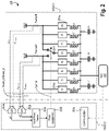
- FIG. 1 illustrates a high-level usage architecture of apparatus 100 of balancing input power from multiple sources, in accordance with some embodiments.
- Apparatus 100 comprises input power supply rails, voltage regulator (VR) bridges and switches 101 , VR controller 102 , and load 103 .
- the VR bridges provide regulated power supply Vout to load 103 .
- Load 103 may have its own VRs to regulate power to various logic domains inside load 103 .
- the VRs of load 103 may use Vout as its input power supply.
- Input power supply rails provide input power supply to the VR bridges from same or different power supply sources.
- the power supply sources may be an AC-DC converter or a DC-DC converter that provides, for example, 12 V DC power supply to the input power supply rails.
- the power supply sources may be coupled to the apparatus via one or more connectors on a board.
- two input supply rails Vin,A and Vin,B are illustrated that may receive power supplies from two different sources.
- any number of input supply rails can be used to provide power to multiple bridges of a voltage regulator (VR).
- VR voltage regulator
- load 103 is to draw maximum power from all input power supply sources. This is only possible if the power drawn is balanced among connectors providing the power supply.
- Some level of input power balance is achieved passively through card design by selectively feeding different VRs, phases or bridges of high-current VRs from appropriate input power supply sources. For example, different voltage rails and/or phases are passively or statically distributed among the various input power sources.
- VR controller 102 senses, measures, and/or estimates (indicated by Sense_A and Sense_B), the current through each power supply rail, voltage of each power supply rail, and/or power of each power supply rail.
- VR controller 102 processes the sensed, measured, and/or estimated values and generates one or more control signals to turn on/off switches that couple or decouple one or more phases (or bridges) from one input power supply rail to another input power supply rail.
- the logic values of the one or more control signals depends on the power limit that can be drawn from the input power supply rails. These values are sensed, measured, and/or estimated values and indicate the imbalance in the amount of power drawn from the input power supply rails.
- VR controller 102 One goal of VR controller 102 is to balance power draw from the various input power supplies (provided on input power supply rails) so that load 103 can operate with maximum power and performance it needs to perform its tasks.
- Load 103 can be any suitable load such as a system-on-chip as discussed with reference to FIG. 16 , a general purpose processor (CPU), a graphics processing unit (GPU), an application specific integrated circuit (ASIC), artificial intelligence processor, an inference chip, a digital signal processor (DSP), etc.
- CPU general purpose processor
- GPU graphics processing unit
- ASIC application specific integrated circuit
- DSP digital signal processor
- VR bridges and switches 101 and/or VR controller 102 are on-board components. In some embodiments, VR bridges and switches 101 and/or VR controller 102 are on a single die. In some embodiments, VR bridges and switches 101 and/or VR controller 102 are within SoC/load 103 .
- FIG. 2 illustrates apparatus 200 where a voltage regulator controller measures two input power sources and sends a control signal to a switch for balancing input power from multiple sources, in accordance with some embodiments.
- Each bridge may comprise a high-side switch and a low-side switch coupled in series with the high-side switch.
- the high-side switch is further coupled to the power supply rail.
- a first set of bridges f 1 , f 2 , f 3 , and f 4 are coupled to a first power supply rail Vin,A while a second set of bridges f 5 , f 6 , f 7 , and f 8 are coupled to a second power supply rail Vin,B.
- VR bridge 201 / 101 also comprises switch SW 1 that is controllable by Control signal from VR controller 102 / 202 .
- Switch SW 1 couples bridge f 5 to the first power supply rail Vin,A or to the second power supply rail Vin,B.
- Switch SW 1 is implemented as a transistor that can be any high voltage transistor of any conductivity type.
- switch SW 1 is an n-type transistor, p-type transistor, or a combination of n-type and p-type transistors.
- a phase e.g., bridge f 5
- Switch SW 1 behaves like a power multiplexer and connects one of the input power sources to one or more phases based on the control signal.
- control signal is a digital signal.
- VR controller 102 / 202 comprises analog-to-digital converters (ADCs) 202 a and 202 b , input power sense circuitry 202 c , phase assignment circuitry 202 d , and communication interface 202 e .
- ADCs 202 a and 202 b are apparatuses that convert continuous physical quantities (e.g., voltages) to digital numbers that represent the amplitude of the physical quantities.
- ADCs 202 a and 202 b convert the analog signals Sense_A (e.g., voltage V insen,A and current I insen,A ) and Sense_B (e.g., voltage V insen,B and current V insen,B ) to their corresponding digital representations d 1 and d 2 , respectively.
- Sense_A e.g., voltage V insen,A and current I insen,A
- Sense_B e.g., voltage V insen,B and current V insen,B
- ADC 202 a/b is one of: direct-conversion ADC (for flash ADC), two-step flash ADC, successive-approximation ADC (SAR ADC), ramp-compare ADC, Wilkinson ADC, integrating ADC, delta-encoded ADC or counter-ramp, pipeline ADC (also called subranging quantizer), sigma-delta ADC (also known as a delta-sigma ADC), time-interleaved ADC, ADC with intermediate FM stage, or time-stretch ADC.
- ADCs 202 a and 202 b are considered to be flash ADCs.
- Input power sense circuitry 202 c receives the digital representations d 1 and d 2 .
- input power sense circuitry 202 c compares the values of d 1 and d 2 against reference codes ref 1 and ref 2 , respectively.
- the same reference code is used to compare with d 1 and d 2 values.
- d 1 and d 2 represent current.
- d 1 and d 2 carry voltage and current information.
- the reference codes are predetermined or programmable.
- the reference code represents the maximum current limit of the power supply rails Vin,A and Vin,B.
- input power sense circuitry 202 c first calculates power based on values within d 1 and d 2 .
- the same reference code is used to compare d 1 and d 2 values.
- the reference codes are predetermined or programmable.
- the maximum power limit of the power supply rails Vin,A and Vin,B represents the maximum power that can be drawn from power supply sources or connectors providing power supply to the power supply rails Vin,A and Vin,B.
- the phase assignment circuitry 202 d receives the output of the comparing.
- phase assignment circuitry 202 d determines whether the digital presentations d 1 and/or d 2 are above a power limit as indicated by the reference code(s). When phase assignment circuitry 202 d determines that the supply rail Vin.A is not fully utilized compared to the supply rail Vin,B, then it sends a control signal to switch SW 1 to couple bridge or phase f 5 to supply rail Vin,A. As such, power demand from the input supply rails Vin,A and Vin,B is substantially balanced. In a similar case, when phase assignment circuitry 202 d determines that the supply rail Vin.B is not fully utilized compared to the supply rail Vin,A, then it sends a control signal to switch SW 1 to couple bridge or phase f 5 to supply rail Vin,B. As such, power demand from input supply rails Vin,A and Vin,B is substantially balanced. This scheme of moving one or more bridge/phases from one input power supply rail to another input power supply rail results in coarse adjustment of input power load balancing.
- VR controller 102 / 202 also monitors loading conditions of SoC 103 .
- VR controller 102 / 202 monitors Vout to determine whether it is at its expected level (e.g., when compared with a reference voltage).
- VR controller 102 / 202 receives Vout information via communication interface 202 e along with sensed power and/or current of the input supply rails, and then adjusts duty cycle of a pulse train signal that drives the high-side and/or low-side switches of each phase or bridge.
- SoC 103 commands a voltage for VR controller 102 / 202 to regulate to.
- all input and output voltage and current measurements are performed by VR controller 102 / 202 .
- the control is passed to SoC 103 via communication interface 202 e .
- SoC 103 then controls switch SW 1 . This implementation reduces the pin count of VR controller 102 / 202 .
- FIG. 3 illustrates apparatus 300 where a sensor converts voltage and current measurements into signal representing power, and this information is used by a voltage regulator controller to send a control signal to a switch for balancing input power from multiple sources, in accordance with some embodiments.
- Apparatus 300 is similar to apparatus 200 but for the type of sense signals (Sense,A, and Sense,B) provided to VR controller 102 / 302 .
- a separate sensor converts the voltage and current measurements (e.g., V insen,A , V insen,B , and I insen,B ) into a signal representing power (e.g., P insen,A and P insen,B ).
- VR bridge circuitry 101 / 301 measures or estimates power through the power supply rails Vin,A and Vin,B.
- a corresponding power sensor is coupled for each power supply rail.
- Power Sensor 301 a couples to sense resistor RsenseA of power supply rail Vin,A
- Power Sensor 301 b couples to sense resistor RsenseB of power supply rail Vin,B.
- Output of Power Sensor 301 a is P insen,A while output of Power Sensor 301 b is P insen,B .
- ADCs 302 a/b are simpler in design than ADCs 202 a/b in that each ADC 302 a/b receives a single analog input signal P insen,A , or P insen,B and converts that to a corresponding digital representation. If a power sensor is used, a single data conversion takes place, in accordance with some embodiments. Otherwise, VR controller 102 / 302 measures voltage and current, converts both quantities, and then multiplies them to get power. Similarly, if current is used to make decisions then a single data conversion takes place, in accordance with some embodiments. The operation of controlling switch SW 1 for coarse adjustment and controlling current through the phases for fine adjustment is same as that explained with reference to FIG. 2 .
- the control is passed to SoC 103 via communication interface 202 e .
- SoC 103 then controls switch SW 1 . This implementation further reduces the pin count of VR controller 102 / 202 .
- FIG. 4 illustrates apparatus 400 where the voltage regulator controller communicates power level to a processor, which in turn decides the control of the switch for balancing input power from multiple sources, in accordance with some embodiments.
- an additional VR driver VR 2 , switch SW 2 , and power supply rail Vin,C is shown for VR bridge 101 / 401 .
- VR Driver VR 2 has two bridges f 1 and f 2 , which couple to two corresponding inductors L 12 and L 22 , which in turn are coupled to capacitor C 12 .
- SW 2 couples bridge/phase f 2 of VR 2 to first supply rail Vin,A.
- SW 2 couples bridge/phase f 2 of VR 2 to third supply rail Vin,C.
- VR driver VR 2 can have any number of bridges of phases where at least one phase or bridge is switchable between first supply rail Vin,A and third supply rail Vin,C. While switch SW 2 is shown to couple phase or bridge f 2 of VR 2 , it can also be used to couple bridge or phase f 1 of VR 1 to third power supply rail Vin,C.
- a sense resistor RsenseC is coupled between VR 2 and third supply rail Vin,C.
- VR controller 102 / 402 receives the sense information from the third input power supply rail Vin,C (e.g., V insen,C and I insen,C ) along with sense information from the first input power supply rail Vin,A (e.g., V insen,A and Iinsen,A ), and the sense information from the second input power supply rail Vin,B (e.g., V insen,B and Iinsen,B ).
- VR controller 102 / 402 includes an additional ADC 402 b to convert the sense information from the third input power supply rail Vin,C (e.g., V insen,C and I insen,C ) into its digital representation d 3 .
- input power sense circuitry 202 c compares the values of d 1 , d 2 , and d 3 against reference codes ref 1 , ref 2 , and ref 3 , respectively. In some embodiments, the same reference code is compared with d 1 , d 2 , and d 3 values.
- the reference codes are predetermined or programmable.
- the reference codes represent the maximum power limit of the power supply rails Vin,A, Vin,B, and Vin,C. For example, ref 1 represents the power limit of Vin,A, ref 2 represents the power limit of Vin,B, and ref 3 represents the power limit of Vin,C.
- phase assignment circuitry 202 d receives the output of the comparing.
- phase assignment circuitry 202 d determines whether the digital presentations d 1 , d 2 , and/or d 3 are above the power limits as indicated by the reference code(s). When phase assignment circuitry 202 d determines that supply rail Vin.A is not fully utilized compared to supply rail Vin,B, then it sends a control signal to switch SW 1 to couple bridge or phase f 5 to supply rail Vin,A. As such, power demand from input supply rails Vin,A and Vin,B is substantially balanced. In a similar case, when phase assignment circuitry 202 d determines that supply rail Vin.B is not fully utilized compared to supply rail Vin,A, then it sends a control signal to switch SW 1 to couple bridge or phase f 5 to supply rail Vin,B.
- phase assignment circuitry 202 d determines that supply rail Vin.A is not fully utilized compared to supply rail Vin,C, then it sends a control signal to switch SW 2 to couple bridge or phase f 2 to supply rail Vin,A. As such, power demand from input supply rails Vin,C and Vin,A is substantially balanced.
- phase assignment circuitry 202 d determines that supply rail Vin.C is not fully utilized compared to supply rail Vin,A, then it sends a control signal to switch SW 2 to couple bridge or phase f 2 to supply rail Vin,C. As such, power demand from input supply rails Vin,A Vin,B, and Vin,C is substantially balanced.
- This scheme of moving one or more bridge/phases from one input power supply rail to another input power supply rail results in coarse adjustment of input power load balancing.
- the controls are passed to SoC 103 via communication interface 202 e .
- SoC 103 then controls switches SW 1 and SW 2 . This implementation further reduces the pin count of VR controller 102 / 402 .
- FIG. 5 illustrates apparatus 500 with more than two input power supply rails, wherein one or more switches are controlled for balancing input power from multiple sources, in accordance with some embodiments.
- Apparatus 500 is similar to apparatus 400 but for the type of sense signals provided to VR controller 102 / 402 .
- separate sensors converts the voltage and current measurements into signals representing power.
- VR bridge circuitry 101 / 501 measures or estimates power through the power supply rails Vin,A Vin,B. and Vin,C In this case, for each power supply rail, a corresponding power sensor is coupled.
- Power Sensor 301 a couples to sense resistor RsenseA of power supply rail Vin,A
- Power Sensor 301 b couples to sense resistor RsenseB of power supply rail Vin,B
- Power Sensor 501 c couples to sense resistor RsenseC of power supply rail Vin,C.
- the output of power sensor 301 a is P insen
- the output of Power Sensor 301 b is P insen,B
- the output of power sensor 501 c is P insen,C .
- ADCs 302 a/b and 502 b are simpler in design than ADCs 202 a/b and 402 a in that each ADC 302 a/b and 501 c receives a single analog input signal P insen,A , P insen,B , or P insen,C and converts that to corresponding digital representations d 1 , d 2 , or d 3 , respectively.
- the operation of controlling switches SW 1 and SW 2 for coarse adjustment and controlling current through the phases for fine adjustment is same as that explained with reference to FIG. 4 .
- the controls are passed to SoC 103 via communication interface 202 e .
- SoC 103 then controls switches SW 1 and SW 2 . This implementation further reduces the pin count of VR controller 102 / 402 .
- FIG. 6 illustrates apparatus 600 showing details of the apparatus of FIG. 5 , where input power of each input sources is sensed, summed, and fed to the VR controller for balancing input power from multiple sources, in accordance with some embodiments.
- Apparatus 600 comprises comparators 601 a , 601 b , and 601 c for each power sensor 301 a , 301 b , and 501 c , respectively.
- Apparatus 600 also includes an OR logic gate 602 that generates the control for SoC 103 .
- SoC 103 also receives the sum P total of P all sensed powers (e.g., P insen,A , P insen,B , P insen,C ).
- Node 603 generates the sum P total of all sensed powers (e.g., P insen,A, Pinsen,B , P insen,C ).
- VR Controller 102 receives P total .
- Comparator 601 a compares P insen,A with reference P limit,A .
- the output of comparator 601 a is Cmp,A.
- Comparator 601 b compares P insen,B with reference P limit,B .
- the output of comparator 601 b is Cmp,B.
- Comparator 601 c compares P insen,C with reference P limit,C .
- the output of comparator 601 c is Cmp,C.
- OR gate 602 performs an OR logic function on Cmp,A, CmpB, and Cmp,C, and generates a control signal for SoC 103 .
- the control signal indicates over-power on one or more power sources.
- SoC 103 then generates the appropriate control signals for the switches SW 1 and/or SW 2 to move the phases or bridges from one power supply rail to another power supply rail to balance the power drawn from the input power supply rails.
- FIG. 7 illustrates apparatus 700 showing details of the apparatus of FIG. 5 , where input current of some but not all input sources is sensed, summed, and fed to the VR controller for balancing input power from multiple sources, in accordance with some embodiments.
- input current of some but not all input sources is sensed, summed, and fed to the VR controller for balancing input power from multiple sources, in accordance with some embodiments.
- the printed circuit board (PCB) layout, stack-up of layers in the PCB, and signal integrity constraints may not allow I insen,A, Iinsen,B , or I insen,C to be summed up at node 703 for VR controller 102 .
- Physically distant power supply sources can have their own current sensors which communicates with SoC 103 independently. SoC 103 then generates the control signals for switches SW 1 and SW 2 .
- Apparatus 700 comprises comparators 702 a and 702 b for a subset of current sensors (or amplifiers) 701 a and 701 b , respectively.
- Current sensor 701 a senses the current through resistor Rsense,A on the first power supply rail Vin,A.
- the current I insen,A is measured by measuring voltage V 1 insen,A and V 2 insen,A across resistor RsenseA.
- Current sensor 701 b senses the current through resistor Rsense,B on the first power supply rail Vin,B.
- the current I insen,B is measured by measuring voltage V 1 insen,B and V 2 insen,B across resistor RsenseB.
- Apparatus 700 also includes an OR logic gate 704 that generates the control for SoC 103 .
- SoC 103 also receives the sum current I total of a subset of sensed or measured currents (e.g., I insen,A and I insenB ).
- Node 703 generates the sum I total of all sensed currents (e.g., I insen,A and I insenB ).
- VR Controller 102 receives I total .
- Comparator 702 a compares I insen,A with reference current limit I insen,A .
- the output of comparator 702 a is Cmp,A.
- Comparator 702 b compares I insen,B with reference current limit P limit,B .
- the output of comparator 702 b is Cmp,B.
- OR gate 602 performs an OR logic function on Cmp,A and CmpB, and generates a control signal for SoC 103 .
- the control current information signal indicates over-power condition on one or more power sources.
- SoC also directly receives power sensed through the third power supply rail Vin,C via Power Sensor 501 c .
- SoC 103 then generates the appropriate control signals for the switches SW 1 and/or SW 2 to move the phases or bridges from one power supply rail to another power supply rail to balance the power drawn from the input power supply rails.
- FIG. 8 illustrates apparatus 800 showing details of a modified apparatus of FIG. 5 , where current measurement and inference of power draw is used for balancing input power from multiple sources, in accordance with some embodiments.
- Apparatus 800 is similar to apparatus 700 but for inferring power draw from the third power supply rail Vin,C.
- SoC 103 knows the current it is consuming and from that information SoC 103 knows power drawn from third power supply rail Vin,C in view of the total current I total .
- I total is the sum of currents I insen,A and I insen,B .
- K pwr is linear gain
- P in,C:Static is an offset power that exists when 0 Watt is measured.
- SoC 103 then generates the appropriate control signals for the switches SW 1 and/or SW 2 to move the phases or bridges from one power supply rail to another power supply rail to balance the power drawn from the input power supply rails.
- FIG. 9 illustrates apparatus 900 showing details of the apparatus of FIG. 5 , where input power of some but not all input sources is sensed, summed, and fed to the VR controller for balancing input power from multiple sources, in accordance with some embodiments.
- the PCB layout, stack-up of layers in the PCB, and signal integrity constraints may not allow power measurements P insen,A , P insen,B , or P insen,C to be summed up at node 903 for VR controller 102 .
- Physically distant power supply sources can have their own power sensors which communicates with SoC 103 independently. SoC 103 then generates the control signals for switches SW 1 and SW 2 .
- Power Sensor 501 c generates its own power measurements and sends it directly to SoC 103 .
- Apparatus 900 comprises comparators 902 a and 902 b for a subset of power sensors 501 a and 501 b , respectively.
- Power Sensor 501 a senses the current through resistor Rsense,A on the first power supply rail Vin,A.
- Apparatus 900 also includes an OR logic gate 704 that generates the control for SoC 103 .
- SoC 103 also receives the sum power P total of a subset of sensed or measured power (e.g., P insen,A and P insenB ).
- Node 903 generates the sum P total of all sensed powers (e.g., P insen,A and P insenB ).
- VR Controller 102 receives P total .
- Comparator 902 a compares P insen,A with reference power limit P limit,A .
- the output of comparator 902 a is Cmp,A.
- Comparator 902 b compares P insen,B with reference power limit P limit,B .
- the output of comparator 902 b is Cmp,B.
- OR gate 704 performs an OR logic function on Cmp,A and CmpB, and generates a control signal for SoC 103 . SoC 103 then generates the appropriate control signals for the switches SW 1 and/or SW 2 in view of the total power, control signal, and power measurement from Power Sensor 501 c to move the phases or bridges from one power supply rail to another power supply rail to balance the power drawn from the input power supply rails.
- the comparators, summation node, and OR gate are positioned in the VR bridge 101 or VR controller 102 .
- FIG. 10 illustrates apparatus 1000 with details of a modified apparatus of FIG. 2 , in accordance with some embodiments.
- phases 1-3 e.g., 201 a 1-3
- phases 4 through Nph e.g., 201 a 4-Nph
- second power rail Vin,B each bridge or phase (e.g., 201 a 1-N ) is shown with a high-side switch MP and a low-side switch MN coupled in series.
- the high-side switch MP is controllable by buffer or driver 201 ab while the low side switch MN is controllable by inverter 201 ai .
- Both the buffer 201 ab and inverter 201 ai are driven by a corresponding pulse width modulated (PWM) signal.
- PWM pulse width modulated
- bridge or phase 201 a 1 is driven by PWM 1
- bridge or phase 201 a 2 is driven by PWM 2
- bridge 201 a Ni is driven by PWM Nph .
- VR controller 102 / 1001 comprises voltage sense circuitry 1002 a , summation node 1002 b , compensation circuitry 1002 c , PWM generator 1002 d , input power sense circuitry 1002 e / 202 c , input power balance circuitry 1002 f , current balance circuitry 1002 g , current sense circuitry 1002 h , resistor ladder 1002 i , and summing node 1002 j.
- voltage sense 1002 a comprises a voltage divider that divides down Vout to a lower representative voltage Vsense.
- Circuitry 1002 b provides Verr′, which is the difference between a modified value of Vref and the sensed voltage. For example, a voltage VLL is subtracted from Vref to generate a modified Vref. The voltage VLL is the product of measured current I total and load-line resistance 1002 i .
- Compensator 1002 c receives Verr.
- Compensator 1002 c generates a modified reference voltage Vfb (feedback voltage) for PWM generator 1002 d.
- PWM generator 1002 d comprises a waveform synthesizer and N comparators or amplifiers.
- the N comparators or amplifiers receive Vfb from compensation circuitry 1002 c and the output of waveform synthesizer, and generates outputs which are the PWM 1-Nph signals for timing control and for bridge drivers 201 ab and 201 ai of bridges 201 a 1-N .
- the output of waveform synthesizer are N number of triangular waves.
- the triangular waves are periodic and have a voltage swing between Vh (high voltage threshold) and V 1 (low voltage reference).
- the waveform synthesizer produces N number of sawtooth waves.
- current balance circuitry 1002 g comprises N current mixers.
- current mixers receive sensed phase currents (i (1-Nph) ) of each bridge from among bridges 201 a 1-N and subtract average current from all bridges 201 a 1-N to generate error currents which are used to generate corresponding voltage for inputs of corresponding comparators of PWM generator 1002 d .
- the feedback voltage (i.e., output of compensation 1002 c ) of each phase (or bridge) is shifted up or down.
- shifting the feedback voltage up increases the PWM duty cycle which increases phase current
- shifting the feedback voltage down decreases the PWM duty cycle which decreases phase current (i.e., from output of bridge from among bridge 201 a 1-N ).
- current balance circuitry 1002 g has a compensation network for individual phase currents to introduce delta duty cycles for each phase in an attempt to balance the current. So each phase duty cycle is the sum of the common duty cycle and current balance duty cycle.
- the VR controller 102 has two loops—main voltage loop and current loop.
- RLL R load-line ;
- the main VR loop (including PWM 1002 d ⁇ bridge drivers 201 a 1-N ⁇ Voltage sense 1002 a ⁇ compensator 1002 c ) regulates the output voltage Vout while the current sensing loop (including current mixers ⁇ comparators ⁇ bridge drivers 201 a 1-N ⁇ current sensors 1002 h ⁇ current balance 1002 g ) checks and maintains that all phases (i.e., bridges 201 a 1-N ) generate the same amount of current.
- current sensor 1002 h is in VR controller 102 . In some embodiments, current sensor 1002 h are within the power stages and the sensed current is received by VR controller 102 .
- Current sense block 1002 h receives current information from all phases and passes individual phase currents and their sum I total to Current Balance 1002 g . I total is also used in the voltage loop for load line (LL). The total current through all phases or bridges 201 a 1-N is I total (e.g., I total is the sum of currents I L1 through I LNph ) I total is converted to a corresponding voltage V total via load-line resistance 1002 i .
- duty cycle of PWM signals is modified, which in turn changes the current flow through bridges 201 a 1-N .
- the output of current balance circuitry 1002 g is ⁇ D 1-Nph .
- FIG. 15A illustrates the generation of ⁇ D 1-Nph .
- Input power sense 202 c / 1002 e senses input signals of the input power supplied by power supply rails Vin,A and Vin,B. In general, Input Power Sense 202 c / 1002 e calculates the measured input power using measured voltage and current, measured power (from an external power sensor), or measured current and programmed voltage (e.g., assume 12V, measure current). SOC 103 receives information sensed by Input Power Sense 202 c / 1002 e through communication 202 e . Power supplied by sources Vin,A and Vin,B are communicated to Input Power Balance 1002 f . Input Power Balance 1002 f generates scaling factors k iA and k iB used in Current Balance 1002 g .
- scaling factors k iA and k iB are generated to balance sources VinA, VinB proportional to their limits (See, e.g., FIG. 13 ). In some embodiments, scaling factors k iA and k iB are generated to balance the available (or unused) power of sources VinA, VinB (See, e.g., FIG. 14 ). In some embodiments, scaling factors k iA , k iB are used to scale the reference current Iref in Current Balance 1002 g (See, e.g., FIG. 15A ). In some embodiments, k iA ,k iB scale the measured phase current I 1 , I 2 , . . . I Nph in Current Balance 1002 g.
- FIG. 11 illustrates apparatus 1100 with details of the apparatus of FIG. 2 , in accordance with some embodiments.
- ADCs 202 a/b provides digital representations of the measured current (and/or voltage) or power through the first and second power supply rails, and this information is provided to power sense 1002 e .
- current sense 1002 h generates digital codes representing the current through each phase.
- ADCs 1102 1-N are provided to convert analog current I L1 though I LNph into corresponding digital representations, and these digital representations are used by current sense 1002 h to generate codes for sensed currents I 1 through I Nph .
- Input power sense 202 c / 1002 e receives digital representation of input signals of the input power supplied by Vin,A and Vin,B.
- d 1 and d 2 contain voltage and current information of sources Vin,A and Vin,B.
- d 1 and d 2 contain current information of sources Vin,A and Vin,B.
- Voltage information required to calculate power may be a programmable value.
- SOC 103 receives information contained in d 1 and d 2 through communication 202 e.
- FIG. 12 illustrates apparatus 1200 details of the apparatus of FIG. 3 where a separate sensor converts the voltage and current measurements into a signal representing power, in accordance with some embodiments.
- a separate sensor converts the voltage and current measurements into a signal representing power, in accordance with some embodiments.
- separate sensors 301 a/b convert the voltage and current measurements into a signal representing power. This saves pins on the VR controller 102 / 1001 .
- FIGS. 13, 14, and 15A and B illustrate control blocks 1300 , 1400 , and 1500 , respectively, with two input power balance loops for balancing input power from multiple sources, in accordance with some embodiments.
- the control blocks 1300 , 1400 , and 1500 correspond to circuitry of input power balance 1002 f and current balance 1003 g .
- two input power balance loops are described.
- the first loop is to balance the power proportional to the capability of the input power supply source (e.g., Vin,A and Vin,B).
- the second loop balances the available power for each input power supply source.
- Control block 1300 comprises summation circuitries 1301 , 1302 , and 1303 , scaling units 1304 and 1305 , compensation networks 1306 and 1308 , and safety limiters 1307 and 1309 .
- P A and P B are the measured power drawn from input power supply rails Vin,A and Vin,B, respectively.
- P TOT is the total power or summation of power drawn from input power supply rails Vin,A and Vin,B.
- P A hits its limit or is near its limit then current is steered from input power supply rail Vin,A to Vin.B.
- Limiters 1307 and 1309 prevent saturation of current through inductors L 1 through L Nph .
- the measured total power P TOT is scaled for each individual source by k A or k B with the target power draw for each power source (e.g., power sources providing power to input power supply rails Vin,A and Vin,B). Power measured for each power source is compared to its target, and the result is compensated by G P to generate ki A and ki B , where k iA and k iB are the current steering coefficients that are used in the current balancing loop.
- Power balancing implemented in control block 1300 can be enabled to run at all times to constantly and continuously balance input power supplies. Alternatively, control block 1300 can be activated to operate under certain conditions. In some embodiments, control block 1300 can be activated when total power P TOT exceeds a limit. In some embodiments, control block 1300 can be activated to balance power when powers P A or P B exceed a limit related to the rated limit of the power source. The limits can be less than or equal to the rated limit of the power sources. The limits can be programmable.
- Control block 1400 includes summation circuitries 1401 , 1402 , 1403 , 1404 in addition to the ones described with reference to control block 1300 .
- P A,ref and P B,ref are individual reference power limits on input power supply rails Vin,A and Vin,B.
- P TOT,ref is the total reference power limit.
- e PA is the error between the measured power P A and limit of Power Source P A,ref .
- e PB is the error between the measured power P B and limit of Power Source P B,ref .
- e PTOT is the error between the total measured power and the limit of the input power supply rails Vin,A and Vin,B (e.g., limit of the sources providing power to these rails).
- the current steering coefficients k iA and k iB are used in the current balancing loop.
- the total error e PTOT is scaled for each individual input power source by k A or k B . Error of each input power source is compared to its target, and the result is compensated by G p to generate ki A and ki B .
- the power balancing loop can operate in one of many configurations. For example, the power balance loop can be always enabled to run at all times to constantly and continuously balance input power supplies.
- the power balance loop can balance if one of the input sources exceeds its limit (P ref ).
- the power balance loop can balance if one of the input sources approaches limit (e.g., passes a threshold lower than the limit).
- the power balance loop can balance when scaled error (e PTOT *k A/B ) approaches a threshold.
- the power balance loop can be used when a difference in scaled errors cross a threshold.
- the power balance loop can be used when the total load power (e.g., VR output power) exceeds a threshold.
- Control loop 1500 illustrates the current balance loop.
- I ref is the average of the total current supplied by the voltage regulator.
- Currents I 1 , I 2 , through I Nph are the measured currents of the individual VR phases.
- k iA and k iB scale the reference current, Gi is a compensation network.
- Each measured phase current is compared to the augmented reference (1+k iA/B ) to create a phase-specific delta duty cycle and to steer the current between phases.
- Increasing current through a phase increases current (hence power) drawn from the supply rail it is connected to.
- Apparatus 1520 calculates the I ref signal required to equalize currents through the phases.
- source Vin A has 75 Watt (W) limit and source Vin,B has 150 W limit for a total limit of 225 W.
- the power drawn by the bridges is 210 W and the measured error for each input power source is 7.5 W.
- the difference between measured error and target error for each source is compensated by G P to generate k iA and k iB .
- FIGS. 15A-B In the current balance loop (e.g., FIGS. 15A-B ), k iA and k iB augments reference to increase/decrease duty cycles of the PWM signal of each phase to draw more/less power for each input power source.
- FIGS. 15 A-B also show the internals of current balance 1002 g.
- a scheme can be used for not balancing the error.
- an input power source is allowed to be drawn at its limit and phases are scaled up on the other input power source(s) to force them to draw more power.
- This scheme effectively clamps one source at its limit and allows the other source to provide more until it also hits its limit.
- one supply is clamped so other supplies are forced to increase until they also reach their limit.
- an input power source is allowed to be drawn at its limit and then current is provided by the supported phases is reduced. This scheme forces all phases (e.g., phases connected to supplies Vin,A and Vin,B) to increase together until they both reach their limits.
- phase current steering is identified on datasheets as a static means of overcoming non-uniform phase heating.
- the scheme can be extended to thermal balancing input power balancing loop. For example, input power is balanced by steering current and thermals are balanced with further steering of current.
- FIG. 16 illustrates a smart device, or a computer system, or a SoC (System-on-Chip) 103 / 2500 that uses the apparatus for balancing input power from multiple sources, according to some embodiments of the disclosure.
- device 2500 represents an appropriate computing device, such as a computing tablet, a mobile phone or smart-phone, a laptop, a desktop, an Internet-of-Things (IOT) device, a server, a wearable device, a set-top box, a wireless-enabled e-reader, or the like. It will be understood that certain components are shown generally, and not all components of such a device are shown in device 2500 .
- IOT Internet-of-Things
- the voltage regulator(s) of the SoC may also steer current through the phases or bridges to balance the power drawn from the input power supply rails.
- the VR(s) may adjust the duty cycle of PWM signals to change the current driven or sunk from high-side and/or low-side switches of the phases or bridges.
- the device 2500 comprises a SoC (System-on-Chip) 2501 .
- SoC System-on-Chip
- An example boundary of the SOC 2501 is illustrated using dotted lines in FIG. 16 , with some example components being illustrated to be included within SOC 2501 —however, SOC 2501 may include any appropriate components of device 2500 .
- device 2500 includes processor 2504 .
- Processor 2504 can include one or more physical devices, such as microprocessors, application processors, microcontrollers, programmable logic devices, processing cores, or other processing means.
- the processing operations performed by processor 2504 include the execution of an operating platform or operating system on which applications and/or device functions are executed.
- the processing operations include operations related to I/O (input/output) with a human user or with other devices, operations related to power management, operations related to connecting computing device 2500 to another device, and/or the like.
- the processing operations may also include operations related to audio I/O and/or display I/O.
- processor 2504 includes multiple processing cores (also referred to as cores) 2508 a , 2508 b , 2508 c . Although merely three cores 2508 a , 2508 b , 2508 c are illustrated, processor 2504 may include any other appropriate number of processing cores, e.g., tens, or even hundreds of processing cores. Processor cores 2508 a , 2508 b , 2508 c may be implemented on a single integrated circuit (IC) chip. Moreover, the chip may include one or more shared and/or private caches, buses or interconnections, graphics and/or memory controllers, or other components.
- IC integrated circuit
- processor 2504 includes cache 2506 .
- sections of cache 2506 may be dedicated to individual cores 2508 (e.g., a first section of cache 2506 dedicated to core 2508 a , a second section of cache 2506 dedicated to core 2508 b , and so on).
- one or more sections of cache 2506 may be shared among two or more of cores 2508 .
- Cache 2506 may be split in different levels, e.g., level 1 (L1) cache, level 2 (L2) cache, level 3 (L3) cache, etc.
- processor core 2504 may include a fetch unit to fetch instructions (including instructions with conditional branches) for execution by the core 2504 .
- the instructions may be fetched from any storage devices such as the memory 2530 .
- Processor core 2504 may also include a decode unit to decode the fetched instruction.
- the decode unit may decode the fetched instruction into a plurality of micro-operations.
- Processor core 2504 may include a schedule unit to perform various operations associated with storing decoded instructions.
- the schedule unit may hold data from the decode unit until the instructions are ready for dispatch, e.g., until all source values of a decoded instruction become available.
- the schedule unit may schedule and/or issue (or dispatch) decoded instructions to an execution unit for execution.
- the execution unit may execute the dispatched instructions after they are decoded (e.g., by the decode unit) and dispatched (e.g., by the schedule unit).
- the execution unit may include more than one execution unit (such as an imaging computational unit, a graphics computational unit, a general-purpose computational unit, etc.).
- the execution unit may also perform various arithmetic operations such as addition, subtraction, multiplication, and/or division, and may include one or more an arithmetic logic units (ALUs).
- ALUs arithmetic logic units
- a co-processor (not shown) may perform various arithmetic operations in conjunction with the execution unit.
- execution unit may execute instructions out-of-order.
- processor core 2504 may be an out-of-order processor core in one embodiment.
- Processor core 2504 may also include a retirement unit.
- the retirement unit may retire executed instructions after they are committed. In an embodiment, retirement of the executed instructions may result in processor state being committed from the execution of the instructions, physical registers used by the instructions being de-allocated, etc.
- the processor core 2504 may also include a bus unit to enable communication between components of the processor core 2504 and other components via one or more buses.
- Processor core 2504 may also include one or more registers to store data accessed by various components of the core 2504 (such as values related to assigned app priorities and/or sub-system states (modes) association.
- device 2500 comprises connectivity circuitries 2531 .
- connectivity circuitries 2531 includes hardware devices (e.g., wireless and/or wired connectors and communication hardware) and/or software components (e.g., drivers, protocol stacks), e.g., to enable device 2500 to communicate with external devices.
- Device 2500 may be separate from the external devices, such as other computing devices, wireless access points or base stations, etc.
- connectivity circuitries 2531 may include multiple different types of connectivity.
- the connectivity circuitries 2531 may include cellular connectivity circuitries, wireless connectivity circuitries, etc.
- Cellular connectivity circuitries of connectivity circuitries 2531 refers generally to cellular network connectivity provided by wireless carriers, such as provided via GSM (global system for mobile communications) or variations or derivatives, CDMA (code division multiple access) or variations or derivatives, TDM (time division multiplexing) or variations or derivatives, 3rd Generation Partnership Project (3GPP) Universal Mobile Telecommunications Systems (UMTS) system or variations or derivatives, 3GPP Long-Term Evolution (LTE) system or variations or derivatives, 3GPP LTE-Advanced (LTE-A) system or variations or derivatives, Fifth Generation (5G) wireless system or variations or derivatives, 5G mobile networks system or variations or derivatives, 5G New Radio (NR) system or variations or derivatives, or other cellular service standards.
- GSM global system for mobile communications
- CDMA code division multiple access
- TDM time division multiplexing
- 3GPP
- Wireless connectivity circuitries (or wireless interface) of the connectivity circuitries 2531 refers to wireless connectivity that is not cellular, and can include personal area networks (such as Bluetooth, Near Field, etc.), local area networks (such as Wi-Fi), and/or wide area networks (such as WiMax), and/or other wireless communication.
- connectivity circuitries 2531 may include a network interface, such as a wired or wireless interface, e.g., so that a system embodiment may be incorporated into a wireless device, for example, cell phone or personal digital assistant.
- device 2500 comprises control hub 2532 , which represents hardware devices and/or software components related to interaction with one or more I/O devices.
- processor 2504 may communicate with one or more of display 2522 , one or more peripheral devices 2524 , storage devices 2528 , one or more other external devices 2529 , etc., via control hub 2532 .
- Control hub 2532 may be a chipset, a Platform Control Hub (PCH), and/or the like.
- PCH Platform Control Hub
- control hub 2532 illustrates one or more connection points for additional devices that connect to device 2500 , e.g., through which a user might interact with the system.
- devices e.g., devices 2529
- devices that can be attached to device 2500 include microphone devices, speaker or stereo systems, audio devices, video systems or other display devices, keyboard or keypad devices, or other I/O devices for use with specific applications such as card readers or other devices.
- control hub 2532 can interact with audio devices, display 2522 , etc.
- input through a microphone or other audio device can provide input or commands for one or more applications or functions of device 2500 .
- audio output can be provided instead of, or in addition to display output.
- display 2522 includes a touch screen
- display 2522 also acts as an input device, which can be at least partially managed by control hub 2532 .
- control hub 2532 manages devices such as accelerometers, cameras, light sensors or other environmental sensors, or other hardware that can be included in device 2500 .
- the input can be part of direct user interaction, as well as providing environmental input to the system to influence its operations (such as filtering for noise, adjusting displays for brightness detection, applying a flash for a camera, or other features).
- control hub 2532 may couple to various devices using any appropriate communication protocol, e.g., PCIe (Peripheral Component Interconnect Express), USB (Universal Serial Bus), Thunderbolt, High Definition Multimedia Interface (HDMI), Firewire, etc.
- PCIe Peripheral Component Interconnect Express
- USB Universal Serial Bus
- Thunderbolt Thunderbolt
- HDMI High Definition Multimedia Interface
- Firewire etc.
- display 2522 represents hardware (e.g., display devices) and software (e.g., drivers) components that provide a visual and/or tactile display for a user to interact with device 2500 .
- Display 2522 may include a display interface, a display screen, and/or hardware device used to provide a display to a user.
- display 2522 includes a touch screen (or touch pad) device that provides both output and input to a user.
- display 2522 may communicate directly with the processor 2504 .
- Display 2522 can be one or more of an internal display device, as in a mobile electronic device or a laptop device or an external display device attached via a display interface (e.g., DisplayPort, etc.).
- display 2522 can be a head mounted display (HMD) such as a stereoscopic display device for use in virtual reality (VR) applications or augmented reality (AR) applications.
- HMD head mounted display
- VR virtual reality
- AR augmented reality
- device 2500 may include Graphics Processing Unit (GPU) comprising one or more graphics processing cores, which may control one or more aspects of displaying contents on display 2522 .
- GPU Graphics Processing Unit
- Control hub 2532 may include hardware interfaces and connectors, as well as software components (e.g., drivers, protocol stacks) to make peripheral connections, e.g., to peripheral devices 2524 .
- software components e.g., drivers, protocol stacks
- device 2500 could both be a peripheral device to other computing devices, as well as have peripheral devices connected to it.
- Device 2500 may have a “docking” connector to connect to other computing devices for purposes such as managing (e.g., downloading and/or uploading, changing, synchronizing) content on device 2500 .
- a docking connector can allow device 2500 to connect to certain peripherals that allow computing device 2500 to control content output, for example, to audiovisual or other systems.
- device 2500 can make peripheral connections via common or standards-based connectors.
- Common types can include a Universal Serial Bus (USB) connector (which can include any of a number of different hardware interfaces), DisplayPort including MiniDisplayPort (MDP), High Definition Multimedia Interface (HDMI), Firewire, or other types.
- USB Universal Serial Bus
- MDP MiniDisplayPort
- HDMI High Definition Multimedia Interface
- Firewire or other types.
- connectivity circuitries 2531 may be coupled to control hub 2532 , e.g., in addition to, or instead of, being coupled directly to the processor 2504 .
- display 2522 may be coupled to control hub 2532 , e.g., in addition to, or instead of, being coupled directly to processor 2504 .
- device 2500 comprises memory 2530 coupled to processor 2504 via memory interface 2534 .
- Memory 2530 includes memory devices for storing information in device 2500 .
- Memory can include nonvolatile (state does not change if power to the memory device is interrupted) and/or volatile (state is indeterminate if power to the memory device is interrupted) memory devices.
- Memory device 2530 can be a dynamic random access memory (DRAM) device, a static random access memory (SRAM) device, flash memory device, phase-change memory device, or some other memory device having suitable performance to serve as process memory.
- DRAM dynamic random access memory
- SRAM static random access memory
- flash memory device phase-change memory device, or some other memory device having suitable performance to serve as process memory.
- memory 2530 can operate as system memory for device 2500 , to store data and instructions for use when the one or more processors 2504 executes an application or process.
- Memory 2530 can store application data, user data, music, photos, documents, or other data, as well as system data (whether long-term or
- Elements of various embodiments and examples are also provided as a machine-readable medium (e.g., memory 2530 ) for storing the computer-executable instructions (e.g., instructions to implement any other processes discussed herein).
- the machine-readable medium e.g., memory 2530
- embodiments of the disclosure may be downloaded as a computer program (e.g., BIOS) which may be transferred from a remote computer (e.g., a server) to a requesting computer (e.g., a client) by way of data signals via a communication link (e.g., a modem or network connection).
- BIOS a computer program
- a remote computer e.g., a server
- a requesting computer e.g., a client
- a communication link e.g., a modem or network connection
- device 2500 comprises temperature measurement circuitries 2540 , e.g., for measuring temperature of various components of device 2500 .
- temperature measurement circuitries 2540 may be embedded, or coupled or attached to various components, whose temperature are to be measured and monitored.
- temperature measurement circuitries 2540 may measure temperature of (or within) one or more of cores 2508 a , 2508 b , 2508 c , voltage regulator 2514 , memory 2530 , a mother-board of SOC 2501 , and/or any appropriate component of device 2500 .
- device 2500 comprises power measurement circuitries 2542 , e.g., for measuring power consumed by one or more components of the device 2500 .
- the power measurement circuitries 2542 may measure voltage and/or current.
- the power measurement circuitries 2542 may be embedded, or coupled or attached to various components, whose power, voltage, and/or current consumption are to be measured and monitored.
- power measurement circuitries 2542 may measure power, current and/or voltage supplied by one or more voltage regulators 2514 , power supplied to SOC 2501 , power supplied to device 2500 , power consumed by processor 2504 (or any other component) of device 2500 , etc.
- device 2500 comprises one or more voltage regulator circuitries, generally referred to as voltage regulator (VR) 2514 VR having a high bandwidth and low power differential-to-single-ended type-III compensator.
- VR 2514 generates signals at appropriate voltage levels, which may be supplied to operate any appropriate components of the device 2500 .
- VR 2514 is illustrated to be supplying signals to processor 2504 of device 2500 .
- VR 2514 receives one or more Voltage Identification (VID) signals, and generates the voltage signal at an appropriate level, based on the VID signals.
- VID Voltage Identification
- Various type of VRs may be utilized for the VR 2514 .
- VR 2514 may include a “buck” VR, “boost” VR, a combination of buck and boost VRs, low dropout (LDO) regulators, switching DC-DC regulators, etc.
- Buck VR is generally used in power delivery applications in which an input voltage needs to be transformed to an output voltage in a ratio that is smaller than unity.
- Boost VR is generally used in power delivery applications in which an input voltage needs to be transformed to an output voltage in a ratio that is larger than unity.
- each processor core has its own VR which is controlled by PCU 2510 a/b and/or PMIC 2512 .
- each core has a network of distributed LDOs to provide efficient control for power management.
- the LDOs can be digital, analog, or a combination of digital or analog LDOs.
- the VR is an adaptive VR that can provide an adaptive voltage output as discussed with reference to various embodiments.
- device 2500 comprises one or more clock generator circuitries, generally referred to as clock generator 2516 .
- Clock generator 2516 generates clock signals at appropriate frequency levels, which may be supplied to any appropriate components of device 2500 .
- clock generator 2516 is illustrated to be supplying clock signals to processor 2504 of device 2500 .
- clock generator 2516 receives one or more Frequency Identification (FID) signals, and generates the clock signals at an appropriate frequency, based on the FID signals.
- FID Frequency Identification
- Clock generator 2516 is an adaptive clock source that can provide an adaptive frequency output as discussed with reference to various embodiments.
- device 2500 comprises battery 2518 supplying power to various components of device 2500 .
- battery 2518 is illustrated to be supplying power to processor 2504 .
- device 2500 may comprise a charging circuitry, e.g., to recharge the battery, based on Alternating Current (AC) power supply received from an AC adapter.
- AC Alternating Current
- device 2500 comprises Power Control Unit (PCU) 2510 (also referred to as Power Management Unit (PMU), Power Controller, etc.).
- PCU Power Control Unit
- some sections of PCU 2510 may be implemented by one or more processing cores 2508 , and these sections of PCU 2510 are symbolically illustrated using a dotted box and labelled PCU 2510 a .
- some other sections of PCU 2510 may be implemented outside the processing cores 2508 , and these sections of PCU 2510 are symbolically illustrated using a dotted box and labelled as PCU 2510 b .
- PCU 2510 may implement various power management operations for device 2500 .
- PCU 2510 may include hardware interfaces, hardware circuitries, connectors, registers, etc., as well as software components (e.g., drivers, protocol stacks), to implement various power management operations for device 2500 .
- device 2500 comprises Power Management Integrated Circuit (PMIC) 2512 , e.g., to implement various power management operations for device 2500 .
- PMIC 2512 is a Reconfigurable Power Management ICs (RPMICs) and/or an IMVP (Intel® Mobile Voltage Positioning).
- RPMICs Reconfigurable Power Management ICs
- IMVP Intelligent Mobile Voltage Positioning
- the PMIC is within an IC chip separate from processor 2504 .
- The may implement various power management operations for device 2500 .
- PMIC 2512 may include hardware interfaces, hardware circuitries, connectors, registers, etc., as well as software components (e.g., drivers, protocol stacks), to implement various power management operations for device 2500 .
- device 2500 comprises one or both PCU 2510 or PMIC 2512 .
- any one of PCU 2510 or PMIC 2512 may be absent in device 2500 , and hence, these components are illustrated using dotted lines.
- Various power management operations of device 2500 may be performed by PCU 2510 , by PMIC 2512 , or by a combination of PCU 2510 and PMIC 2512 .
- PCU 2510 and/or PMIC 2512 may select a power state (e.g., P-state) for various components of device 2500 .
- PCU 2510 and/or PMIC 2512 may select a power state (e.g., in accordance with the ACPI (Advanced Configuration and Power Interface) specification) for various components of device 2500 .
- ACPI Advanced Configuration and Power Interface
- PCU 2510 and/or PMIC 2512 may cause various components of the device 2500 to transition to a sleep state, to an active state, to an appropriate C state (e.g., C0 state, or another appropriate C state, in accordance with the ACPI specification), etc.
- PCU 2510 and/or PMIC 2512 may control a voltage output by VR 2514 (e.g., SCVR) and/or a frequency of a clock signal output by the clock generator, e.g., by outputting the VID signal and/or the FID signal, respectively.
- PCU 2510 and/or PMIC 2512 may control battery power usage, charging of battery 2518 , and features related to power saving operation.
- the clock generator 2516 can comprise a phase locked loop (PLL), frequency locked loop (FLL), or any suitable clock source.
- each core of processor 2504 has its own clock source. As such, each core can operate at a frequency independent of the frequency of operation of the other core.
- PCU 2510 and/or PMIC 2512 performs adaptive or dynamic frequency scaling or adjustment. For example, clock frequency of a processor core can be increased if the core is not operating at its maximum power consumption threshold or limit.
- PCU 2510 and/or PMIC 2512 determines the operating condition of each core of a processor, and opportunistically adjusts frequency and/or power supply voltage of that core without the core clocking source (e.g., PLL of that core) losing lock when the PCU 2510 and/or PMIC 2512 determines that the core is operating below a target performance level. For example, if a core is drawing current from a power supply rail less than a total current allocated for that core or processor 2504 , then PCU 2510 and/or PMIC 2512 can temporality increase the power draw for that core or processor 2504 (e.g., by increasing clock frequency and/or power supply voltage level) so that the core or processor 2504 can perform at higher performance level. As such, voltage and/or frequency can be increased temporality for processor 2504 without violating product reliability.
- the core clocking source e.g., PLL of that core
- PCU 2510 and/or PMIC 2512 may perform power management operations, e.g., based at least in part on receiving measurements from power measurement circuitries 2542 , temperature measurement circuitries 2540 , charge level of battery 2518 , and/or any other appropriate information that may be used for power management.
- PMIC 2512 is communicatively coupled to one or more sensors to sense/detect various values/variations in one or more factors having an effect on power/thermal behavior of the system/platform. Examples of the one or more factors include electrical current, voltage droop, temperature, operating frequency, operating voltage, power consumption, inter-core communication activity, etc.
- sensors may be provided in physical proximity (and/or thermal contact/coupling) with one or more components or logic/IP blocks of a computing system. Additionally, sensor(s) may be directly coupled to PCU 2510 and/or PMIC 2512 in at least one embodiment to allow PCU 2510 and/or PMIC 2512 to manage processor core energy at least in part based on value(s) detected by one or more of the sensors.
- processors 2504 may execute application programs 2550 , Operating System 2552 , one or more Power Management (PM) specific application programs (e.g., generically referred to as PM applications 2558 ), and/or the like. PM applications 2558 may also be executed by the PCU 2510 and/or PMIC 2512 .
- OS 2552 may also include one or more PM applications 2556 a , 2556 b , 2556 c .
- the OS 2552 may also include various drivers 2554 a , 2554 b , 2554 c , etc., some of which may be specific for power management purposes.
- device 2500 may further comprise a Basic Input/Output System (BIOS) 2520 . BIOS 2520 may communicate with OS 2552 (e.g., via one or more drivers 2554 ), communicate with processors 2504 , etc.
- BIOS Basic Input/Output System
- PM applications 2558 , 2556 , drivers 2554 , BIOS 2520 , etc. may be used to implement power management specific tasks, e.g., to control voltage and/or frequency of various components of device 2500 , to control wake-up state, sleep state, and/or any other appropriate power state of various components of device 2500 , control battery power usage, charging of the battery 2518 , features related to power saving operation, etc.
- first embodiment may be combined with a second embodiment anywhere the particular features, structures, functions, or characteristics associated with the two embodiments are not mutually exclusive.
- Example 1 An apparatus comprising: a first power supply rail to provide a first power supply as input to a first set of bridges, wherein the first set of bridges is coupled to a first set of inductors; a second power supply rail to provide a second power supply as input to a second set of bridges, wherein the second set of bridges is coupled to a second set of inductors; and a controller to monitor electrical characteristics associated with the first and second power supply rails, and to control one or more switches to substantially balance power received by the first and second set of bridges, wherein the one or more switches are coupled to the first and second bridges and the first and second power supply rails.
- Example 2 The apparatus of example 1, wherein an individual bridge of the first set of bridges is to provide a first phase to a load, wherein an individual bridge of the second set of bridges is to provide a second phase to the load, and wherein the first phase is different from the second phase.
- Example 3 The apparatus of example 2, wherein the load is a system-on-chip.
- Example 4 The apparatus of example 1, wherein the controller is to close the one or more switches to move a phase of a bridge of the first set of bridges to the second set of bridges if the second set of bridges demands less power from the second power supply rail than the first set of bridges demand from the first power supply rail.
- Example 5 The apparatus of example 1, wherein the controller is to adjust a duty cycle of a drive signal to each bridge of the first and/or second set of bridges to introduce current inequality between the bridges.
- Example 6 The method of example 5, wherein the current inequality between the first and second set of bridges is introduced in response to measured input power.
- Example 7 The method of example 5, wherein the current inequality between the first and second set of bridges is introduced in response to measured input current.
- Example 8 The apparatus of example 1, wherein the controller comprises: a first analog-to-digital converter coupled to a first resistor between the first power supply rail and the first set of bridges, wherein the first analog-to-digital converter is to receive a first voltage of the first power supply rail and a first current through the first power supply rail towards the first set of bridges.
- Example 9 The apparatus of example 8, wherein the controller comprises: a second analog-to-digital converter coupled to a second resistor between the second power supply rail and the second set of bridges, wherein the second analog-to-digital converter is to receive a second voltage of the first power supply rail and a second current through the second power supply rail towards the second set of bridges.
- Example 10 The apparatus of example 1 comprises: a first power sensor to measure first power through the first power supply rail; and a second power sensor to measure second power through the second power supply rail.
- Example 11 The apparatus of example 10, wherein the controller comprises: a first analog-to-digital converter coupled to an output of the first power sensor, wherein the first analog-to-digital converter is to convert the first measured power to a digital representation of the measured power; and a second analog-to-digital converter coupled to an output of the second power sensor, wherein the second analog-to-digital converter is to convert the second measured power to a digital representation of the measured power.
- Example 12 The apparatus of example 10 comprises a node to sum the measured first and second powers, and provide the sum to the controller.
- Example 13 The apparatus of example 10 comprises: a first comparator to compare the first measured power with a first reference power; and a second comparator to compare the second measured power to a second reference power; and an OR gate to perform an OR logic function with outputs of the first and second comparators, wherein an output of the OR gate is provided to a load.
- Example 14 An apparatus comprising: a first power supply rail to provide a first power supply as input to a first set of bridges, wherein the first set of bridges is coupled to a first set of inductors; a second power supply rail to provide a second power supply as input to a second set of bridges, wherein the second set of bridges is coupled to a second set of inductors; and a controller to balance power drawn from the first and second power supply rails via: a coarse adjustment of one or more phases of the first and second set of bridges; and a fine adjust of current through the one or more phases of the first and second set of bridges.
- Example 15 The apparatus of example 14, wherein the controller is to monitor electrical characteristics associated with the first and second power supply rails.
- Example 16 The apparatus of example 15, wherein the electrical characteristics include one or more of current through the first and second power supply rails, or power associated with the first and second power supply rails.
- Example 17 The apparatus of example 14, wherein the controller is to control one or more switches for the coarse adjustment to substantially balance power received by the first and second set of bridges, wherein the one or more switches are coupled to the first and second bridges and the first and second power supply rails.
- Example 18 The apparatus of example 12, wherein the controller is to adjust a duty cycle of a drive signal to each bridge of the first and/or second set of bridges to introduce current inequality between the bridges, wherein the current inequality between the first and second set of bridges is introduced in response to measured input power; or wherein the current inequality between the first and second set of bridges is introduced in response to measured input current.
- Example 19 A system comprising: a first set of inductors; a first power supply rail to provide a first power supply as input to a first set of bridges, wherein the first set of bridges is coupled to the first set of inductors; a second set of inductors; a second power supply rail to provide a second power supply as input to a second set of bridges, wherein the second set of bridges is coupled to the second set of inductors; and a system-on-chip coupled to the first and second set of inductors; one or more switches are coupled to the first and second bridges and the first and second power supply rails; a voltage regulator (VR) controller to monitor electrical characteristics associated with the first and second power supply rails, and to dynamically control the one or more switches to substantially balance power received by the first and second set of bridges.
- VR voltage regulator
- Example 20 The system of example 19, wherein the VR controller is to close the one or more switches to move a phase of a bridge of the first set of bridges to the second set of bridges if the second set of bridges demands less power from the second power supply rail than the first set of bridges demand from the first power supply rail.
- Example 21 The system of example 19, wherein the VR controller is to adjust a duty cycle of a drive signal to each bridge of the first and/or second set of bridges to balance current flow through the bridge.
- Example 22 The system of example 19, wherein an individual bridge of the first set of bridges is to provide a first phase to a load, wherein an individual bridge of the second set of bridges is to provide a second phase to the load, and wherein the first phase is different from the second phase.
Landscapes
- Engineering & Computer Science (AREA)
- Theoretical Computer Science (AREA)
- Physics & Mathematics (AREA)
- General Physics & Mathematics (AREA)
- Power Engineering (AREA)
- Electromagnetism (AREA)
- Radar, Positioning & Navigation (AREA)
- Automation & Control Theory (AREA)
- General Engineering & Computer Science (AREA)
- Dc-Dc Converters (AREA)
Abstract
Description
P in,measured =P in,A +P in,B
P in,total =P in,measured +P in,C:model
P in,total =P in,measured +K pwe P in,measured +P in,C:Static
P in,total=(1+K pwr)P in,measured +P in,C:static
e PTOT=(P A,ref +P B,ref)−(P A +P B)
Claims (24)
Priority Applications (2)
| Application Number | Priority Date | Filing Date | Title |
|---|---|---|---|
| US16/792,073 US11474547B2 (en) | 2020-02-14 | 2020-02-14 | Apparatus and method of balancing input power from multiple sources |
| EP20213743.6A EP3866323A1 (en) | 2020-02-14 | 2020-12-14 | Apparatus and method of balancing input power from multiple sources |
Applications Claiming Priority (1)
| Application Number | Priority Date | Filing Date | Title |
|---|---|---|---|
| US16/792,073 US11474547B2 (en) | 2020-02-14 | 2020-02-14 | Apparatus and method of balancing input power from multiple sources |
Publications (2)
| Publication Number | Publication Date |
|---|---|
| US20210255650A1 US20210255650A1 (en) | 2021-08-19 |
| US11474547B2 true US11474547B2 (en) | 2022-10-18 |
Family
ID=73835398
Family Applications (1)
| Application Number | Title | Priority Date | Filing Date |
|---|---|---|---|
| US16/792,073 Active 2040-09-23 US11474547B2 (en) | 2020-02-14 | 2020-02-14 | Apparatus and method of balancing input power from multiple sources |
Country Status (2)
| Country | Link |
|---|---|
| US (1) | US11474547B2 (en) |
| EP (1) | EP3866323A1 (en) |
Cited By (1)
| Publication number | Priority date | Publication date | Assignee | Title |
|---|---|---|---|---|
| US20230246551A1 (en) * | 2018-10-10 | 2023-08-03 | Samsung Electronics Co., Ltd. | Multi-phase switching regulator including interleaving circuit and switching regulating method using the same |
Families Citing this family (5)
| Publication number | Priority date | Publication date | Assignee | Title |
|---|---|---|---|---|
| US20220014149A1 (en) * | 2020-02-27 | 2022-01-13 | Robert Bruce Ganton | System and apparatus for generating dynamic reference voltage in power constrained devices |
| US11424752B2 (en) * | 2020-11-06 | 2022-08-23 | AyDeeKay LLC | Interleaved analog-to-digital converter (ADC) gain calibration |
| US11601063B2 (en) * | 2021-01-08 | 2023-03-07 | Astec International Limited | Power supply unit with autonomous input power limiting |
| KR20220121385A (en) * | 2021-02-25 | 2022-09-01 | 삼성전자주식회사 | Application processor and electronic device including same |
| US20240158063A1 (en) * | 2022-11-11 | 2024-05-16 | Brunswick Corporation | Electric marine propulsion system and control method |
Citations (17)
| Publication number | Priority date | Publication date | Assignee | Title |
|---|---|---|---|---|
| US5814972A (en) * | 1993-05-13 | 1998-09-29 | Canon Kabushiki Kaisha | Electronic apparatus having multiple loads, driven by plural batteries |
| US6177783B1 (en) | 1999-09-13 | 2001-01-23 | Adc Telecommunications, Inc. | Current balancing for voltage regulator having inputs from multiple power supplies |
| US6215290B1 (en) | 1999-11-15 | 2001-04-10 | Semtech Corporation | Multi-phase and multi-module power supplies with balanced current between phases and modules |
| US7498694B2 (en) * | 2006-04-12 | 2009-03-03 | 02Micro International Ltd. | Power management system with multiple power sources |
| US20130038289A1 (en) * | 2010-02-20 | 2013-02-14 | Lawrence Tze-Leung Tse | Battery-cell converter systems |
| US8856557B2 (en) | 2010-06-03 | 2014-10-07 | International Business Machines Corporation | Digital power balancing controller |
| US20150002095A1 (en) * | 2012-02-09 | 2015-01-01 | Mitsubishi Electric Corporation | Parallel electricity-storage system and control method thereof |
| US9100757B2 (en) * | 2012-07-02 | 2015-08-04 | Apple Inc. | Headset impedance detection |
| US9553449B2 (en) * | 2014-05-08 | 2017-01-24 | Fujitsu Limited | Power supply apparatus, method of controlling power supply, and base station apparatus |
| US10027135B2 (en) * | 2015-09-30 | 2018-07-17 | Silergy Semiconductor Technology (Hangzhou) Ltd | Apparatus for balancing battery power |
| US10069414B2 (en) | 2015-04-01 | 2018-09-04 | Infineon Technologies Austria Ag | Switching voltage regulator input voltage and current sensing |
| US10218355B2 (en) * | 2013-09-27 | 2019-02-26 | Renesas Electronics Corporation | Power supply circuit and control method thereof |
| US10270262B2 (en) * | 2015-12-21 | 2019-04-23 | Samsung Electronics Co., Ltd. | Battery control method and apparatus, and battery pack |
| US10311253B2 (en) * | 2013-08-22 | 2019-06-04 | Siemens Ag Österreich | Method for protecting an integrated circuit against unauthorized access |
| US10889190B2 (en) * | 2016-04-20 | 2021-01-12 | Lsis Co., Ltd. | Apparatus for controlling electric vehicle charging system |
| US20210257841A1 (en) * | 2020-02-17 | 2021-08-19 | Samsung Electronics Co., Ltd. | Semiconductor circuit |
| US11152860B2 (en) * | 2018-10-10 | 2021-10-19 | Samsung Electronics Co., Ltd. | Multi-phase switching regulator including interleaving circuit and switching regulating method using the same |
Family Cites Families (3)
| Publication number | Priority date | Publication date | Assignee | Title |
|---|---|---|---|---|
| JP5205083B2 (en) * | 2008-03-07 | 2013-06-05 | ルネサスエレクトロニクス株式会社 | Power supply |
| US9385609B2 (en) * | 2014-02-14 | 2016-07-05 | Infineon Technologies Ag | Analog current estimation and digital estimation correction for a multiphase buck converter |
| US11379708B2 (en) * | 2018-08-09 | 2022-07-05 | Nvidia Corporation | Techniques for efficiently operating a processing system based on energy characteristics of instructions and machine learning |
-
2020
- 2020-02-14 US US16/792,073 patent/US11474547B2/en active Active
- 2020-12-14 EP EP20213743.6A patent/EP3866323A1/en active Pending
Patent Citations (17)
| Publication number | Priority date | Publication date | Assignee | Title |
|---|---|---|---|---|
| US5814972A (en) * | 1993-05-13 | 1998-09-29 | Canon Kabushiki Kaisha | Electronic apparatus having multiple loads, driven by plural batteries |
| US6177783B1 (en) | 1999-09-13 | 2001-01-23 | Adc Telecommunications, Inc. | Current balancing for voltage regulator having inputs from multiple power supplies |
| US6215290B1 (en) | 1999-11-15 | 2001-04-10 | Semtech Corporation | Multi-phase and multi-module power supplies with balanced current between phases and modules |
| US7498694B2 (en) * | 2006-04-12 | 2009-03-03 | 02Micro International Ltd. | Power management system with multiple power sources |
| US20130038289A1 (en) * | 2010-02-20 | 2013-02-14 | Lawrence Tze-Leung Tse | Battery-cell converter systems |
| US8856557B2 (en) | 2010-06-03 | 2014-10-07 | International Business Machines Corporation | Digital power balancing controller |
| US20150002095A1 (en) * | 2012-02-09 | 2015-01-01 | Mitsubishi Electric Corporation | Parallel electricity-storage system and control method thereof |
| US9100757B2 (en) * | 2012-07-02 | 2015-08-04 | Apple Inc. | Headset impedance detection |
| US10311253B2 (en) * | 2013-08-22 | 2019-06-04 | Siemens Ag Österreich | Method for protecting an integrated circuit against unauthorized access |
| US10218355B2 (en) * | 2013-09-27 | 2019-02-26 | Renesas Electronics Corporation | Power supply circuit and control method thereof |
| US9553449B2 (en) * | 2014-05-08 | 2017-01-24 | Fujitsu Limited | Power supply apparatus, method of controlling power supply, and base station apparatus |
| US10069414B2 (en) | 2015-04-01 | 2018-09-04 | Infineon Technologies Austria Ag | Switching voltage regulator input voltage and current sensing |
| US10027135B2 (en) * | 2015-09-30 | 2018-07-17 | Silergy Semiconductor Technology (Hangzhou) Ltd | Apparatus for balancing battery power |
| US10270262B2 (en) * | 2015-12-21 | 2019-04-23 | Samsung Electronics Co., Ltd. | Battery control method and apparatus, and battery pack |
| US10889190B2 (en) * | 2016-04-20 | 2021-01-12 | Lsis Co., Ltd. | Apparatus for controlling electric vehicle charging system |
| US11152860B2 (en) * | 2018-10-10 | 2021-10-19 | Samsung Electronics Co., Ltd. | Multi-phase switching regulator including interleaving circuit and switching regulating method using the same |
| US20210257841A1 (en) * | 2020-02-17 | 2021-08-19 | Samsung Electronics Co., Ltd. | Semiconductor circuit |
Cited By (2)
| Publication number | Priority date | Publication date | Assignee | Title |
|---|---|---|---|---|
| US20230246551A1 (en) * | 2018-10-10 | 2023-08-03 | Samsung Electronics Co., Ltd. | Multi-phase switching regulator including interleaving circuit and switching regulating method using the same |
| US12323062B2 (en) * | 2018-10-10 | 2025-06-03 | Samsung Electronics Co., Ltd. | Multi-phase switching regulator including interleaving circuit and switching regulating method using the same |
Also Published As
| Publication number | Publication date |
|---|---|
| EP3866323A1 (en) | 2021-08-18 |
| US20210255650A1 (en) | 2021-08-19 |
Similar Documents
| Publication | Publication Date | Title |
|---|---|---|
| US11474547B2 (en) | Apparatus and method of balancing input power from multiple sources | |
| US11658570B2 (en) | Seamless non-linear voltage regulation control to linear control apparatus and method | |
| EP3907866B1 (en) | Accurate load current sensing apparatus and method | |
| US11757357B2 (en) | Hybrid digital linear and switched capacitor voltage regulator | |
| US12164319B2 (en) | Dual loop voltage regulator | |
| US11205962B2 (en) | Real-time switching period estimation apparatus and method | |
| US10976764B2 (en) | Differential to single-ended high bandwidth compensator | |
| US11742754B2 (en) | Enhanced constant-on-time buck intellectual property apparatus and method | |
| EP4092896B1 (en) | Computational current sensor | |
| US12051976B2 (en) | Dual-folded boot-strap based buck-boost converter | |
| US12113442B2 (en) | Stacked buck converter with inductor switching node pre-charge and conduction modulation control | |
| US12117469B2 (en) | Per-part real-time load-line measurement apparatus and method | |
| KR20220040376A (en) | Processor peak current control apparatus and method | |
| US11336270B2 (en) | Fuse-less self-start controller | |
| US11429172B2 (en) | Digital linear regulator clamping method and apparatus | |
| US12537433B2 (en) | Device, system and method to deliver power with phase circuits of an integrated circuit die |
Legal Events
| Date | Code | Title | Description |
|---|---|---|---|
| FEPP | Fee payment procedure |
Free format text: ENTITY STATUS SET TO UNDISCOUNTED (ORIGINAL EVENT CODE: BIG.); ENTITY STATUS OF PATENT OWNER: LARGE ENTITY |
|
| AS | Assignment |
Owner name: INTEL CORPORATION, CALIFORNIA Free format text: ASSIGNMENT OF ASSIGNORS INTEREST;ASSIGNORS:TSCHIRHART, DARRYL;WU, ALAN;LEE PACK, JASON;AND OTHERS;SIGNING DATES FROM 20200212 TO 20200214;REEL/FRAME:051845/0934 |
|
| STPP | Information on status: patent application and granting procedure in general |
Free format text: DOCKETED NEW CASE - READY FOR EXAMINATION |
|
| STPP | Information on status: patent application and granting procedure in general |
Free format text: NON FINAL ACTION MAILED |
|
| STPP | Information on status: patent application and granting procedure in general |
Free format text: RESPONSE TO NON-FINAL OFFICE ACTION ENTERED AND FORWARDED TO EXAMINER |
|
| STPP | Information on status: patent application and granting procedure in general |
Free format text: NOTICE OF ALLOWANCE MAILED -- APPLICATION RECEIVED IN OFFICE OF PUBLICATIONS |
|
| STPP | Information on status: patent application and granting procedure in general |
Free format text: PUBLICATIONS -- ISSUE FEE PAYMENT VERIFIED |
|
| STCF | Information on status: patent grant |
Free format text: PATENTED CASE |
|
| MAFP | Maintenance fee payment |
Free format text: PAYMENT OF MAINTENANCE FEE, 4TH YEAR, LARGE ENTITY (ORIGINAL EVENT CODE: M1551); ENTITY STATUS OF PATENT OWNER: LARGE ENTITY Year of fee payment: 4 |