US11462537B2 - Semiconductor device - Google Patents
Semiconductor device Download PDFInfo
- Publication number
- US11462537B2 US11462537B2 US16/919,300 US202016919300A US11462537B2 US 11462537 B2 US11462537 B2 US 11462537B2 US 202016919300 A US202016919300 A US 202016919300A US 11462537 B2 US11462537 B2 US 11462537B2
- Authority
- US
- United States
- Prior art keywords
- pattern
- lower pattern
- device isolation
- isolation layer
- stack
- Prior art date
- Legal status (The legal status is an assumption and is not a legal conclusion. Google has not performed a legal analysis and makes no representation as to the accuracy of the status listed.)
- Active
Links
Images


Classifications
-
- H01L27/0924—
-
- H10W10/0145—
-
- H—ELECTRICITY
- H10—SEMICONDUCTOR DEVICES; ELECTRIC SOLID-STATE DEVICES NOT OTHERWISE PROVIDED FOR
- H10D—INORGANIC ELECTRIC SEMICONDUCTOR DEVICES
- H10D84/00—Integrated devices formed in or on semiconductor substrates that comprise only semiconducting layers, e.g. on Si wafers or on GaAs-on-Si wafers
- H10D84/80—Integrated devices formed in or on semiconductor substrates that comprise only semiconducting layers, e.g. on Si wafers or on GaAs-on-Si wafers characterised by the integration of at least one component covered by groups H10D12/00 or H10D30/00, e.g. integration of IGFETs
- H10D84/82—Integrated devices formed in or on semiconductor substrates that comprise only semiconducting layers, e.g. on Si wafers or on GaAs-on-Si wafers characterised by the integration of at least one component covered by groups H10D12/00 or H10D30/00, e.g. integration of IGFETs of only field-effect components
- H10D84/83—Integrated devices formed in or on semiconductor substrates that comprise only semiconducting layers, e.g. on Si wafers or on GaAs-on-Si wafers characterised by the integration of at least one component covered by groups H10D12/00 or H10D30/00, e.g. integration of IGFETs of only field-effect components of only insulated-gate FETs [IGFET]
- H10D84/85—Complementary IGFETs, e.g. CMOS
- H10D84/853—Complementary IGFETs, e.g. CMOS comprising FinFETs
-
- H—ELECTRICITY
- H10—SEMICONDUCTOR DEVICES; ELECTRIC SOLID-STATE DEVICES NOT OTHERWISE PROVIDED FOR
- H10D—INORGANIC ELECTRIC SEMICONDUCTOR DEVICES
- H10D84/00—Integrated devices formed in or on semiconductor substrates that comprise only semiconducting layers, e.g. on Si wafers or on GaAs-on-Si wafers
- H10D84/80—Integrated devices formed in or on semiconductor substrates that comprise only semiconducting layers, e.g. on Si wafers or on GaAs-on-Si wafers characterised by the integration of at least one component covered by groups H10D12/00 or H10D30/00, e.g. integration of IGFETs
- H10D84/82—Integrated devices formed in or on semiconductor substrates that comprise only semiconducting layers, e.g. on Si wafers or on GaAs-on-Si wafers characterised by the integration of at least one component covered by groups H10D12/00 or H10D30/00, e.g. integration of IGFETs of only field-effect components
- H10D84/83—Integrated devices formed in or on semiconductor substrates that comprise only semiconducting layers, e.g. on Si wafers or on GaAs-on-Si wafers characterised by the integration of at least one component covered by groups H10D12/00 or H10D30/00, e.g. integration of IGFETs of only field-effect components of only insulated-gate FETs [IGFET]
- H10D84/834—Integrated devices formed in or on semiconductor substrates that comprise only semiconducting layers, e.g. on Si wafers or on GaAs-on-Si wafers characterised by the integration of at least one component covered by groups H10D12/00 or H10D30/00, e.g. integration of IGFETs of only field-effect components of only insulated-gate FETs [IGFET] comprising FinFETs
-
- H—ELECTRICITY
- H10—SEMICONDUCTOR DEVICES; ELECTRIC SOLID-STATE DEVICES NOT OTHERWISE PROVIDED FOR
- H10D—INORGANIC ELECTRIC SEMICONDUCTOR DEVICES
- H10D30/00—Field-effect transistors [FET]
- H10D30/60—Insulated-gate field-effect transistors [IGFET]
- H10D30/611—Insulated-gate field-effect transistors [IGFET] having multiple independently-addressable gate electrodes influencing the same channel
-
- H—ELECTRICITY
- H01—ELECTRIC ELEMENTS
- H01L—SEMICONDUCTOR DEVICES NOT COVERED BY CLASS H10
- H01L23/00—Details of semiconductor or other solid state devices
- H01L23/52—Arrangements for conducting electric current within the device in operation from one component to another, i.e. interconnections, e.g. wires, lead frames
- H01L23/535—Arrangements for conducting electric current within the device in operation from one component to another, i.e. interconnections, e.g. wires, lead frames including internal interconnections, e.g. cross-under constructions
-
- H01L29/42392—
-
- H—ELECTRICITY
- H10—SEMICONDUCTOR DEVICES; ELECTRIC SOLID-STATE DEVICES NOT OTHERWISE PROVIDED FOR
- H10D—INORGANIC ELECTRIC SEMICONDUCTOR DEVICES
- H10D30/00—Field-effect transistors [FET]
- H10D30/60—Insulated-gate field-effect transistors [IGFET]
- H10D30/62—Fin field-effect transistors [FinFET]
- H10D30/6215—Fin field-effect transistors [FinFET] having multiple independently-addressable gate electrodes
-
- H—ELECTRICITY
- H10—SEMICONDUCTOR DEVICES; ELECTRIC SOLID-STATE DEVICES NOT OTHERWISE PROVIDED FOR
- H10D—INORGANIC ELECTRIC SEMICONDUCTOR DEVICES
- H10D30/00—Field-effect transistors [FET]
- H10D30/60—Insulated-gate field-effect transistors [IGFET]
- H10D30/67—Thin-film transistors [TFT]
- H10D30/6729—Thin-film transistors [TFT] characterised by the electrodes
- H10D30/673—Thin-film transistors [TFT] characterised by the electrodes characterised by the shapes, relative sizes or dispositions of the gate electrodes
- H10D30/6735—Thin-film transistors [TFT] characterised by the electrodes characterised by the shapes, relative sizes or dispositions of the gate electrodes having gates fully surrounding the channels, e.g. gate-all-around
-
- H—ELECTRICITY
- H10—SEMICONDUCTOR DEVICES; ELECTRIC SOLID-STATE DEVICES NOT OTHERWISE PROVIDED FOR
- H10D—INORGANIC ELECTRIC SEMICONDUCTOR DEVICES
- H10D30/00—Field-effect transistors [FET]
- H10D30/60—Insulated-gate field-effect transistors [IGFET]
- H10D30/67—Thin-film transistors [TFT]
- H10D30/6757—Thin-film transistors [TFT] characterised by the structure of the channel, e.g. transverse or longitudinal shape or doping profile
-
- H—ELECTRICITY
- H10—SEMICONDUCTOR DEVICES; ELECTRIC SOLID-STATE DEVICES NOT OTHERWISE PROVIDED FOR
- H10D—INORGANIC ELECTRIC SEMICONDUCTOR DEVICES
- H10D30/00—Field-effect transistors [FET]
- H10D30/60—Insulated-gate field-effect transistors [IGFET]
- H10D30/791—Arrangements for exerting mechanical stress on the crystal lattice of the channel regions
- H10D30/795—Arrangements for exerting mechanical stress on the crystal lattice of the channel regions being in lateral device isolation regions, e.g. STI
-
- H—ELECTRICITY
- H10—SEMICONDUCTOR DEVICES; ELECTRIC SOLID-STATE DEVICES NOT OTHERWISE PROVIDED FOR
- H10D—INORGANIC ELECTRIC SEMICONDUCTOR DEVICES
- H10D84/00—Integrated devices formed in or on semiconductor substrates that comprise only semiconducting layers, e.g. on Si wafers or on GaAs-on-Si wafers
- H10D84/01—Manufacture or treatment
- H10D84/0123—Integrating together multiple components covered by H10D12/00 or H10D30/00, e.g. integrating multiple IGBTs
- H10D84/0126—Integrating together multiple components covered by H10D12/00 or H10D30/00, e.g. integrating multiple IGBTs the components including insulated gates, e.g. IGFETs
- H10D84/0165—Integrating together multiple components covered by H10D12/00 or H10D30/00, e.g. integrating multiple IGBTs the components including insulated gates, e.g. IGFETs the components including complementary IGFETs, e.g. CMOS devices
- H10D84/0172—Manufacturing their gate conductors
- H10D84/0177—Manufacturing their gate conductors the gate conductors having different materials or different implants
-
- H10W10/021—
-
- H10W10/17—
-
- H10W10/20—
-
- H10W20/20—
Definitions
- Embodiments relate to a semiconductor device.
- a high dielectric layer-metal gate structure has been proposed instead of a general field effect transistor including a gate insulation layer and a gate electrode formed using silicon oxide and polysilicon, respectively.
- a length of a gate and a length of a channel thereunder become small.
- a manufacturing process and structure of an integrated circuit device are variously studied to improve an operation stability and reliability of transistors, which are factors for determining a performance of the integrated circuits.
- Embodiments are directed to a semiconductor device, including a substrate, a first lower pattern and a second lower pattern on the substrate and arranged in a line in a first direction, a first active pattern stack disposed on and spaced apart from the first lower pattern, a second active pattern stack disposed on and spaced apart from the first lower pattern, a fin-cut gate structure disposed on the first lower pattern and overlapping a portion of the first lower pattern, a first gate structure surrounding the first active pattern stack and extending in a second direction crossing the first direction, a second gate structure surrounding the second active pattern stack and extending in the second direction, and a device isolation layer between the first gate structure and the second gate structure and separating the first lower pattern and the second lower pattern.
- Embodiments are also directed to a semiconductor device, including a substrate, a lower pattern disposed on the substrate and extending in a first direction parallel to an upper surface of the substrate, a plurality of sheet patterns disposed on the lower pattern and arranged in a second direction that is perpendicular to the upper surface of the substrate, a gate electrode surrounding the plurality of sheet patterns, and an insulation pattern contacting the plurality of sheet patterns and including a linear insulation pattern and a plurality of protruding insulation patterns.
- the linear insulation pattern may extend in the second direction, and each of the plurality of protruding insulation patterns may protrudes in the first direction from a sidewall of the linear insulation pattern.
- Embodiments are also directed to a semiconductor device, including a substrate including a first region and a second region, a first lower pattern in the first region and extending in a first direction, a second lower pattern in the second region and extending in a second direction, a first active pattern stack on the first lower pattern, the first active pattern stack including a plurality of first sheet patterns, a second active pattern stack on the second lower pattern, the second active pattern stack including a plurality of second sheet patterns, a first gate structure surrounding the plurality of first sheet patterns, a second gate structure surrounding the plurality of second sheet patterns, a first device isolation layer extending along a sidewall of the first gate structure and contacting the first lower pattern, and a second device isolation layer extending along a sidewall of the second gate structure and contacting the second lower pattern.
- the first device isolation layer may include a first portion between an upper surface of the first lower pattern and an uppermost surface of the first active pattern stack
- the second device isolation layer may include a second portion between an upper surface of the second lower pattern and the uppermost surface of the second active pattern
- the first portion of the first device isolation layer may have a first width in the first direction
- the second portion of the second device isolation layer may have a second width in the second direction greater than the first width
- FIG. 1 illustrates a plan view of a semiconductor device according to an example embodiment.
- FIG. 2 illustrates a cross-sectional view taken along line A-A of FIG. 1 .
- FIG. 3 illustrates a cross-sectional view taken along line B-B of FIG. 1 .
- FIG. 4 illustrates an enlarged view of portion X of FIG. 2 .
- FIG. 5 illustrates an enlarged view of portion Y of FIG. 2 .
- FIG. 6 illustrates a view of a semiconductor device according to an example embodiment.
- FIG. 7 illustrates a view of a semiconductor device according to an example embodiment.
- FIG. 8 illustrates a view of a semiconductor device according to an example embodiment.
- FIG. 9 illustrates a view of a semiconductor device according to an example embodiment.
- FIG. 10 illustrates a view of a semiconductor device according to an example embodiment.
- FIG. 11 illustrates a view of a semiconductor device according to an example embodiment.
- FIG. 12 illustrates a view of a semiconductor device according to an example embodiment.
- FIG. 13 illustrates a view of a semiconductor device according to an example embodiment.
- FIG. 14 illustrates a view of a semiconductor device according to an example embodiment.
- FIG. 15 illustrates a plan view of a semiconductor device according to an example embodiment.
- FIG. 16 illustrates a cross-sectional view taken along line C-C of FIG. 15 .
- FIG. 17 illustrates a cross-sectional view taken along line D-D of FIG. 15 .
- FIG. 18 illustrates a view of a semiconductor device according to an example embodiment.
- FIG. 19 illustrates a view of a semiconductor device according to an example embodiment.
- FIG. 20 illustrates a view of a semiconductor device according to an example embodiment.
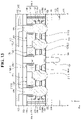
- FIG. 1 is a plan view illustrating a semiconductor device according to an example embodiment.
- FIG. 2 is a cross-sectional view taken along line A-A of FIG. 1 .
- FIG. 3 is a cross-sectional view taken along line B-B of FIG. 1 .
- FIG. 4 is an enlarged view of portion X of FIG. 2 .
- FIG. 5 is an enlarged view of portion Y of FIG. 2 .
- a semiconductor device may include a substrate 100 , a first lower pattern 110 , a second lower pattern 210 , first active pattern stacks 115 and 115 _ 1 , a first fin-cut pattern stack 116 , contacts 175 and 275 , a wiring structure 180 , interlayer insulation layers 191 , 192 , and 193 , second active pattern stacks 215 and 215 _ 1 , a second fin-cut pattern stack 216 , a second fin-cut pattern stack 216 , first gate structures 120 and 120 _ 1 , second gate structures 220 and 220 _ 1 , a first fin-cut gate structure 120 _ 2 , a second fin-cut gate structure 220 _ 2 , and a first device isolation layer 160 .
- the interlayer insulation layers 191 , 192 , and 193 , the contacts 175 and 275 , and the wiring structure 180 are omitted.
- the substrate 100 may be, for example, a bulk silicon substrate or a silicon-on-insulator (SOI) substrate.
- the substrate 100 may include for example, silicon germanium, silicon germanium on insulator (SGOI), indium antimonide, lead tellurium compound, indium arsenide, indium phosphide, gallium arsenide or gallium antimonide, etc.
- the first lower pattern 110 and the second lower pattern 210 may protrude from the substrate 100 .
- the first lower pattern 110 and the second lower pattern 210 may respectively extend lengthwise along a first direction X 1 parallel to an upper surface of the substrate 100 .
- the first lower pattern 110 and the second lower pattern 210 may be arranged in a line in the first direction X 1 and may be spaced apart from each other in the first direction X 1 .
- a long sidewall of the first lower pattern 110 and a long sidewall of the second lower pattern 210 that extend in the first direction X 1 may be defined by a fin trench 105 t .
- one of short sidewalls of the first lower pattern 110 and one of short sidewalls of the second lower pattern 210 that extend in a second direction Y 1 crossing the first direction X 1 may be defined by the fin trench 105 t .
- the short sidewall of the first lower pattern 110 and the short sidewall of the second lower pattern 210 may be defined by a first device isolation trench 160 t .
- Each of the first lower pattern 110 and the second lower pattern 210 may have, for example, a fin type shape.
- first lower pattern 110 and the second lower pattern 210 may be completely separated by the first device isolation trench 160 t .
- a semiconductor pattern for connecting a lower portion of the first lower pattern 110 and a lower portion of the second lower pattern 210 may be disposed between the first device isolation layer 160 and the substrate 100 .
- Each of the first lower pattern 110 and the second lower pattern 210 may be formed by etching a portion of the substrate 100 or may include an epitaxial layer grown from the substrate 100 .
- Each of the first lower pattern 110 and the second lower pattern 210 may include a semiconductor material, for example, silicon (Si) or germanium (Ge).
- each of the first lower pattern 110 and the second lower pattern 210 may include a compound semiconductor, for example, a group IV-IV compound semiconductor or a group III-V compound semiconductor.
- the group IV-IV compound semiconductor may include a binary compound or a ternary compound including at least two of carbon (C), silicon (Si), germanium (Ge), and tin (Sn), or a compound doped with a group IV element.
- the group III-V compound semiconductor may include a binary compound, a ternary compound, or a quaternary compound, each of which is formed by combination of a group III element, for example, at least one of aluminum (Al), gallium (Ga), and indium (In), and a group V element, for example, one of phosphorus (P), arsenic (As), and antimony (Sb).
- the first lower pattern 110 and the second lower pattern 210 may include the same material.
- the field insulation layer 105 may be formed on the substrate 100 .
- the field insulation layer 105 may fill at least a portion of the fin trench 105 t .
- the field insulation layer 105 may be disposed on a sidewall of the first lower pattern 110 and a sidewall of the second lower pattern 210 .
- the field insulation layer 105 may include, for example, at least one of silicon oxide, silicon nitride, and silicon oxynitride.
- the first active pattern stacks 115 and 115 _ 1 and the first fin-cut pattern stack 116 may be disposed on the first lower pattern 110 , and may be spaced apart from the first lower pattern 110 in a thickness direction Z of the substrate 100 .
- the first active pattern stacks 115 and 115 _ 1 and the first fin-cut pattern stack 116 may respectively include one or more sheet patterns 115 NS, 115 NS_ 1 , and 116 NS that are arranged in the thickness direction Z of the substrate 100 .
- the first active pattern stacks 115 and 115 _ 1 and the first fin-cut pattern stack 116 may respectively include a plurality of sheet patterns 115 NS, 115 NS_ 1 , and 116 NS.
- each of the first active pattern stacks 115 and 115 _ 1 and the first fin-cut pattern stack 116 may include three sheet patterns.
- the first active pattern stacks 115 and 115 _ 1 may include a first normal pattern stack 115 and a first dummy pattern stack 115 _ 1 .
- the first active pattern stacks 115 and 115 _ 1 and the first fin-cut pattern stack 116 may be arranged in the first direction X 1 along an upper surface of the first lower pattern 110 .
- a first epitaxial pattern 150 may be disposed between respective ones of the first active pattern stacks 115 and 115 _ 1 and the first fin-cut pattern stack 116 .
- the first normal pattern stack 115 may be connected to two first epitaxial patterns 150 at opposite sides of the first normal pattern stack 115 .
- Each of the first dummy pattern stack 115 _ 1 and the first fin-cut pattern stack 116 may be connected to one first epitaxial pattern 150 .
- the first fin-cut pattern stack 116 may be disposed on one end portion of the first lower pattern 110 defined by the fin trench 105 t .
- the first dummy pattern stack 115 _ 1 may be disposed on another end portion of the first lower pattern 110 defined by the first device isolation trench 160 t.
- the second active pattern stacks 215 and 215 _ 1 and the second fin-cut pattern stack 216 may be disposed on the second lower pattern 210 . and may be spaced apart from the second lower pattern 210 in the thickness direction Z of the substrate 100 .
- the second active pattern stacks 215 and 215 _ 1 and the second fin-cut pattern stack 216 may respectively include one or more sheet patterns 215 NS, 215 NS_ 1 , and 216 NS that are arranged in the thickness direction Z of the substrate 100 .
- the second active pattern stacks 215 and 215 _ 1 may include a second normal pattern stack 215 and a second dummy pattern stack 215 _ 1 .
- the second active pattern stacks 215 and 215 _ 1 and the second fin-cut pattern stack 216 may be arranged in the first direction X 1 along an upper surface of the second lower pattern 210 .
- a second epitaxial pattern 250 may be disposed between respective ones of the second active pattern stacks 215 and 215 _ 1 and the second fin-cut pattern stack 216 .
- the second normal pattern stack 215 may be connected to two second epitaxial patterns 250 at opposite sides of the second normal pattern stack 215 .
- Each of the second dummy pattern stack 215 _ 1 and the second fin-cut pattern stack 216 may be connected to one second epitaxial pattern 250 .
- the second fin-cut pattern stack 216 may be disposed on one end portion of the second lower pattern 210 defined by the fin trench 105 t .
- the second dummy pattern stack 215 _ 1 may be disposed on another end portion of the second lower pattern 210 defined by the first device isolation trench 160 t.
- Each of the first active pattern stacks 115 and 115 _ 1 , the first fin-cut pattern stack 116 , the second active pattern stacks 215 and 215 _ 1 , and the second fin-cut pattern stack 216 may include silicon, germanium, or compound semiconductor, such as a group Iv-Iv compound semiconductor or a group III-v compound semiconductor.
- the first active pattern stacks 115 and 115 _ 1 , the first fin-cut pattern stack 116 , the second active pattern stacks 215 and 215 _ 1 , and the second fin-cut pattern stack 216 that are located at the same level may include the same material.
- the first normal pattern stack 115 and the second normal pattern stack 215 may be used as channel regions of transistors of the same conductive type.
- the first gate structures 120 and 120 _ 1 and the first fin-cut gate structure 120 _ 2 may extend in the second direction Y 1 and may traverse the first lower pattern 110 .
- the first gate structures 120 and 120 _ 1 and the first fin-cut gate structure 120 _ 2 may be disposed on the first lower pattern 110 .
- the first fin-cut gate structure 120 _ 2 may overlap a portion of the first lower pattern 110 .
- the first gate structures 120 and 120 _ 1 may overlap the first lower pattern 110 .
- an overlapping width between the first fin-cut gate structure 120 _ 2 and the first lower pattern 110 in the first direction X 1 may be smaller than a width of the first fin-cut gate structure 120 _ 2 in the first direction X 1 .
- An overlapping width between each of the first gate structures 120 and 120 _ 1 and the first lower pattern 110 may be the same as a width of each of the first gate structures 120 and 120 _ 1 in the first direction X 1 .
- the first gate structures 120 and 120 _ 1 may surround the first active pattern stacks 115 and 115 _ 1 , respectively.
- the first gate structures 120 and 120 _ 1 may include a first normal gate structure 120 surrounding the first normal pattern stack 115 and a first dummy gate structure 120 _ 1 surrounding the first dummy pattern stack 115 _ 1 .
- the first fin-cut gate structure 120 _ 2 may cover the first fin-cut pattern stack 116 .
- the second gate structures 220 and 220 _ 1 and the second fin-cut gate structure 220 _ 2 may extend in the second direction Y 1 and may traverse the second lower pattern 210 .
- the second gate structures 220 and 220 _ 1 and the second fin-cut gate structure 220 _ 2 may be disposed on the second lower pattern 210 .
- the second fin-cut gate structure 220 _ 2 may overlap a portion of the second lower pattern 210 .
- the second gate structures 220 and 220 _ 1 may overlap the second lower pattern 210 .
- the second gate structures 220 and 220 _ 1 may surround the second active pattern stacks 215 and 215 _ 1 , respectively.
- the second gate structures 220 and 220 _ 1 may include a second normal gate structure 220 surrounding the second normal pattern stack 215 and a second dummy gate structure 220 _ 1 surrounding the second dummy pattern stack 215 _ 1 .
- the second fin-cut gate structure 220 _ 2 may cover the second fin-cut pattern stack 216 .
- Each of the first gate structures 120 and 120 _ 1 and the first fin-cut gate structure 120 _ 2 may include a first gate electrode 130 , a first gate insulation layer 135 , first gate spacers 140 , and a first capping pattern 145 .
- Each of the second gate structures 220 and 220 _ 1 and the second fin-cut gate structure 220 _ 2 may include a second gate electrode 230 , a second gate insulation layer 235 , second gate spacers 240 , and a second capping pattern 245 .
- the first gate structures 120 and 120 _ 1 and the first fin-cut gate structure 120 _ 2 will be further described. Descriptions of the second gate structures 220 and 220 _ 1 and the second fin-cut gate structure 220 _ 2 may easily be understood through descriptions of the first gate structures 120 and 120 _ 1 and the first fin-cut gate structure 120 _ 2 .
- the first gate spacers 140 may extend in the second direction Y 1 .
- the first gate spacers 140 may cross the first active pattern stacks 115 and 115 _ 1 and the first fin-cut pattern stack 116 .
- the first gate spacers 140 may be disposed on opposite ends of each of the first active pattern stacks 115 and 115 _ 1 extending in the first direction X 1 .
- the first normal sheet patterns 115 NS and the first dummy sheet patterns 115 NS_ 1 may penetrate the first gate spacers 140 that are opposite to each other.
- the first fin-cut sheet pattern 116 NS may penetrate one of the first gate spacers 140 that are opposite to each other.
- Each of the first gate spacers 140 may include a first inner spacer 142 and a first outer spacer 141 .
- the first inner spacer 142 may disposed between the first lower pattern 110 and each of the first active pattern stacks 115 and 115 _ 1 , between the first lower pattern 110 and the first fin-cut pattern stack 116 , and between respective ones of the sheet patterns 115 NS, 115 NS_ 1 , and 116 NS that are adjacent to each other in the thickness direction Z of the substrate 100 .
- the first outer spacer 141 may be disposed on each of the first active pattern stacks 115 and 115 _ 1 and the first fin-cut pattern stack 116 .
- the first outer spacer 141 and the first inner spacer 142 may include, for example, silicon nitride (SiN), silicon oxynitride (SiON), silicon oxide (SiO 2 ), silicon oxycarbonitride (SiOCN), silicon boron nitride (SiBN), silicon oxyboronitride (SiOBN), silicon oxycarbide (SiOC), or a combination thereof.
- the first inner spacer 142 may be a single layer.
- the first gate insulation layer 135 may extend along a surface of each of the first active pattern stacks 115 and 115 _ 1 and the first fin-cut pattern stack 116 .
- the first gate insulation layer 135 may be disposed on an upper surface of the field insulation layer 105 and on the first lower pattern 110 .
- the first gate insulation layer 135 may extend along inner sidewalls of the first gate spacers 140 .
- An interfacial layer may be disposed between the first gate insulation layer 135 and each of the first active pattern stacks 115 and 115 _ 1 , between the first gate insulation layer 135 and the first fin-cut pattern stack 116 , between the first gate insulation layer 135 and the first lower pattern 110 .
- the first gate insulation layer 135 may include silicon oxide, silicon oxynitride, silicon nitride, and/or a high-k dielectric material having a higher dielectric constant than silicon oxide.
- the first gate insulation layer 135 may include the high-k dielectric material, for example, hafnium oxide, hafnium silicon oxide, hafnium aluminum oxide, lanthanum oxide, lanthanum aluminum oxide, zirconium oxide, zirconium silicon oxide, tantalum oxide, titanium oxide, barium strontium titanium oxide, barium titanium oxide, strontium titanium oxide, yttrium oxide, aluminum oxide, lead scandium tantalum oxide, and/or lead zinc niobate.
- a boundary between the first inner spacer 142 and the first gate insulation layer 135 may be curved, for example.
- the first gate electrode 130 may surround the surface of each of the first active pattern stacks 115 and 115 _ 1 and the first fin-cut pattern stack 116 .
- the first gate electrode 130 may be disposed on the first gate insulation layer 135 , between the first gate spacers 140 .
- the first gate electrode 130 may include, for example, titanium nitride (TiN), tantalum carbide (TaC), tantalum nitride (TaN), titanium silicon nitride (TiSiN), tantalum silicon nitride (TaSiN), tantalum titanium nitride (TaTiN), titanium aluminum nitride (TiAlN), tantalum aluminum nitride (TaAlN), tungsten nitride (WN), ruthenium (Ru).
- TiN titanium nitride
- TaC tantalum carbide
- TaN tantalum nitride
- TiSiN titanium silicon nitride
- TaSiN tantalum silicon nitride
- TaTiN tantalum titanium nitride
- TiAlN titanium aluminum nitride
- TaAlN tantalum aluminum nitride
- WN tungsten nitride
- the first gate electrode 130 may include conductive metal oxide
- the first capping pattern 145 may be disposed on the first gate electrode 130 .
- the first gate insulation layer 135 may not be disposed between the first gate spacers 140 and the first capping pattern 145 .
- the first capping pattern 145 may be disposed between the inner sidewalls of the first gate spacers 140 , but the inventive concept is not limited thereto.
- upper surfaces of the first gate spacers 140 may be recessed lower than an upper surface of a first interlayer insulation layer 191 to be formed in a subsequent process, like the first gate electrode 130 .
- the first capping pattern 145 may be disposed on the upper surfaces of the first gate spacers 140 and an upper surface of the first gate electrode 130 .
- the first capping pattern 145 may be coplanar with the upper surface of the first interlayer insulation layer 191 .
- the first capping pattern 145 may include a material having an etch selectivity with respect to a material of the first interlayer insulation layer 191 .
- the first capping pattern 145 may include, for example, silicon nitride (SiN), silicon oxynitride (SiON), silicon oxide (SiO 2 ), silicon carbonitride (SiCN), silicon oxycarbonitride (SiOCN), or a combination thereof.
- a first epitaxial pattern 150 may be disposed between respective ones of the first gate structures 120 and 120 _ 1 and the first fin-cut gate structure 120 _ 2 .
- the first epitaxial pattern 150 may be disposed on the first lower pattern 110 .
- a second epitaxial pattern 250 may be disposed between respective ones of the second gate structures 220 and 220 _ 1 and the second fin-cut gate structure 220 _ 2 .
- the second epitaxial pattern 250 may be disposed on the second lower pattern 210 .
- the first epitaxial pattern 150 and the second epitaxial pattern 250 may be formed by an epitaxial growth process.
- the first epitaxial pattern 150 may be included in a source/drain of the transistor utilizing the first normal pattern stack 115 as the channel region.
- the second epitaxial pattern 250 may be included in a source/drain of the transistor utilizing the second normal pattern stack 215 as the channel region.
- a first etch stop layer 170 may be disposed on an upper surface of the first epitaxial pattern 150 , an upper surface of the second epitaxial pattern 250 , outer sidewalls of the first gate spacers 140 , outer sidewalls of the second gate spacers 240 , and an upper surface of the field insulation layer 105 .
- the first etch stop layer 170 may include, for example, silicon nitride (SiN), silicon oxynitride (SiON), silicon oxide (SiO 2 ), silicon oxycarbonitride (SiOCN), or a combination thereof.
- the first etch stop layer 170 may include a material having an etch selectivity with respect to the material of the first interlayer insulation layer 191 .
- the first interlayer insulation layer 191 may be disposed on the first etch stop layer 170 .
- the first interlayer insulation layer 191 may cover the outer sidewalls of the first gate spacers 140 and the outer sidewalls of the second gate spacers 240 .
- the first interlayer insulation layer 191 may include, for example, silicon oxide, silicon nitride, and/or silicon oxynitride.
- a second interlayer insulation layer 192 may be disposed on the first interlayer insulation layer 191 .
- the second interlayer insulation layer 192 may cover the first gate structures 120 and 120 _ 1 , the first fin-cut gate structure 120 _ 2 , the second gate structures 220 and 220 _ 1 , and the second fin-cut gate structure 220 _ 2 .
- the second interlayer insulation layer 192 may include, for example, at least one of silicon oxide, silicon nitride, and silicon oxynitride.
- the first device isolation layer 160 may be disposed between the first lower pattern 110 and the second lower pattern 210 .
- the first device isolation layer 160 may separate the first lower pattern 110 and the second lower pattern 210 .
- the first device isolation layer 160 may be disposed between the first gate structure (i.e., the first dummy gate structure) 120 _ 1 and the second gate structure (i.e., the second dummy gate structure) 220 _ 1 .
- the first device isolation layer 160 may extend along a sidewall of the first dummy gate structure 120 _ 1 and a sidewall of the second dummy gate structure 220 _ 1 .
- the first device isolation layer 160 may fill the first device isolation trench 160 t .
- a portion of the first device isolation trench 160 t may be defined by the first lower pattern 110 and the second lower pattern 210 .
- the first device isolation layer 160 may extend between the first dummy gate structure 120 _ 1 and the second dummy gate structure 220 _ 1 , between the first dummy pattern stack 115 _ 1 and the second dummy pattern stack 215 _ 1 , and between the first lower pattern 110 and the second lower pattern 210 .
- the first device isolation layer 160 may extend lengthwise in the thickness direction Z of the substrate 100 .
- the first device isolation layer 160 may contact the first dummy pattern stack 115 _ 1 and the second dummy pattern stack 215 _ 1 .
- the first device isolation layer 160 may contact the first inner spacer 142 and the second inner spacer 242 .
- the first inner spacer 142 and the second inner spacer 242 may protrude in the first direction X 1 from a sidewall 160 s of the first device isolation layer 160 .
- a height from the upper surface of the first lower pattern 110 to an upper surface of the first device isolation layer 160 may be greater than a height from the upper surface of the first lower pattern 110 to an upper surface of the first dummy gate structure 120 _ 1 .
- the height from the upper surface of the first lower pattern 110 to the upper surface of the first device isolation layer 160 may be equal to the height from the upper surface of the first lower pattern 110 to the upper surface of the first dummy gate structure 120 _ 1 .
- the first device isolation layer 160 may have a first width W 11 in the first direction X 1 .
- the first device isolation layer 160 may have a second width W 12 in the first direction X 1 .
- the first width W 11 of the first device isolation layer 160 may be equal to the second width W 12 of the first device isolation layer 160 .
- the uppermost surface of the first dummy pattern stack 115 _ 1 may be an upper surface of an uppermost one of the first dummy sheet patterns 115 NS_ 1 included in the first dummy pattern stack 115 _ 1 .
- the first width W 11 of the first device isolation layer 160 may be a distance between an outer sidewall of the first outer spacer 141 and an outer sidewall of the second outer sidewall 241 , on the uppermost surface of the first dummy pattern stack 115 _ 1 .
- the first device isolation layer 160 may include a first portion contacting the first lower pattern 110 and the second lower pattern 210 , a second portion between the upper surface of the first lower pattern 110 and the uppermost surface of the first dummy pattern stack 115 _ 1 , and a third portion between the uppermost surface of the first dummy pattern stack 115 _ 1 and the upper surface of the first dummy gate structure 120 _ 1 .
- the first portion of the first device isolation layer 160 may have a third width W 13 in the first direction X 1 .
- the third width W 13 of the first portion of the first device isolation layer 160 may be smaller than the second width W 12 of the first device isolation layer 160 .
- the third width W 13 of the first device isolation layer 160 may increase.
- the third width W 13 of the first portion of the first device isolation layer 160 may decrease in a direction from the upper surface of the first lower pattern 110 to the substrate 100 .
- the second portion of the first device isolation layer 160 may have a fourth width W 14 in the first direction X 1 .
- the fourth width W 14 of the second portion of the first device isolation layer 160 may be constant.
- the fourth width W 14 of the second portion of the first device isolation layer 160 may be constant between the upper surface of the first lower pattern 110 and the uppermost surface of the first dummy pattern stack 115 _ 1 .
- the sidewall 160 s of the first device isolation layer 160 may include a fine unevenness.
- the width is constant means that a distance between opposite sidewalls 160 s of the first device isolation layer 160 is exactly equal but a fine variation in the width generated due to the fine unevenness of the sidewall 160 s of the first device isolation layer 160 is included.
- a portion of the first etch stop layer 170 may be disposed between the third portion of the first device isolation layer 160 and the first dummy gate structure 120 _ 1 .
- portion of the first etch stop layer 170 may be disposed along a portion of the outer sidewall of the first outer spacer 141 .
- the third portion of the first device isolation layer 160 may include a second sub region 160 b and a first sub region 160 a on the second sub region 160 b .
- a width of the first sub region 160 a in the first direction X 1 may be smaller than a width of the second sub region 160 b in the first direction X 1 .
- the first device isolation layer 160 may cross between two first lower patterns 110 and two second lower patterns 210 , but the inventive concept is not limited thereto.
- the first device isolation layer 160 , the first inner spacer 142 , and the second inner spacer 242 may constitute an insulation pattern.
- the insulation pattern may include a linear insulation pattern extending lengthwise in the thickness direction Z of the substrate 100 and protruding insulation patterns protruding in the first direction X 1 from the linear insulation pattern and contacting the linear insulation pattern.
- the linear insulation pattern may be a first device isolation layer 160
- each of the protruding insulation patterns may be the first inner spacer 142 and the second inner spacer 242 .
- the protruding insulation patterns may contact a plurality of first dummy sheet patterns 115 NS_ 1 and a plurality of second dummy sheet patterns 215 NS_ 1 .
- the linear insulation pattern may contact the first lower pattern 110 and the second lower pattern 210 .
- the protruding insulation patterns may be disposed on an upper surface of the first lower pattern 110 and an upper surface of the second lower pattern 210 . Since each of the protruding insulation patterns is the first inner spacer 142 and the second inner spacer 242 , a portion of the first dummy sheet pattern 115 NS_ 1 and a portion of the second dummy sheet pattern 215 NS_ 1 may be disposed between the protruding insulation patterns that are adjacent to each other in the thick direction Z of the substrate 100 .
- a first contact 175 and a second contact 275 may be disposed in the second interlayer insulation layer 192 and the first interlayer insulation layer 191 .
- the first contact 175 may be connected to the first epitaxial pattern 150 on the first lower pattern 110 .
- the second contact 275 may be connected to the second epitaxial pattern 250 on the second lower pattern 210 .
- a silicide layer may be disposed between the first contact 175 and the first epitaxial pattern 150 and between the second contact 275 and the second epitaxial pattern 250 .
- the first contact 175 may be connected to one first epitaxial pattern 150
- the second contact 275 may be connected to one second epitaxial pattern 250 .
- an upper surface of the first contact 175 , an upper surface of the second contact 275 , the upper surface of the first device isolation layer 160 , and an upper surface of the second interlayer insulation layer 192 may be coplanar with each other.
- a height from the upper surface of the first lower pattern 110 to the upper surface of the first contact 175 may be equal to a height from the upper surface of the first lower pattern 110 to the upper surface of the first device isolation layer 160 .
- the height is equal means that heights of two positions are exactly equal but a fine difference in the height generated due to a process margin is included.
- the third interlayer insulation layer 193 may be disposed on the second interlayer insulation layer 192 .
- the third interlayer insulation layer 193 may be disposed on the first contact 175 , the second contact 275 , and the first device isolation layer 160 .
- the third interlayer insulation layer 193 may include, for example, at least one of silicon oxide, silicon nitride, silicon oxynitride.
- a wiring structure 180 may be disposed on the third interlayer insulation layer 193 .
- the wiring structure 180 may be formed in a back-end-of-line (BEOL) process.
- the wiring structure 180 may be connected to the first contact 175 and the second contact 275 .
- the wiring structure 180 may include a via pattern 181 and a wiring pattern 182 .
- each of the first contact 175 , the second contact 275 , and the wiring structure 180 is shown to be a single layer, this is merely an example.
- FIG. 6 is a view illustrating a semiconductor device according to an example embodiment.
- FIG. 7 is a view illustrating a semiconductor device according to an example embodiment.
- FIGS. 6 and 7 are enlarged views of portion X of FIG. 2 . The same elements as described with reference to FIGS. 1 to 5 will not be described again or will be briefly mentioned.
- the first inner spacer 142 may have a double-layered structure.
- the first inner spacer 142 may include double layers including different materials.
- the first inner spacer 142 may include an outer protruding insulation layer 142 a and an inner protruding insulation layer 142 b .
- the outer protruding insulation layer 142 a and the inner protruding insulation layer 142 b may contact the first device isolation layer 160 .
- the outer protruding insulation layer 142 a may contact the first gate insulation layer 135 .
- the inner protruding insulation layer 142 b may be disposed between the first device isolation layer 160 and the outer protruding insulation layer 142 a .
- the outer protruding insulation layer 142 a may include silicon nitride, and the inner protruding insulation layer 142 b may include silicon oxide.
- the first inner spacer 142 may include the outer protruding insulation layer 142 a and an inner air gap insulation layer 142 c .
- the outer protruding insulation layer 142 a and the inner air gap insulation layer 142 c may contact the first device isolation layer 160 .
- the inner air gap insulation layer 142 c may include an air gap.
- the air gap may be disposed between the outer protruding insulation layer 142 a and the first device isolation layer 160 .
- the second inner spacer 242 may have the same double-layered structure as the first inner spacer 142 . In an example embodiment, the second inner spacer 242 may have a doubled-layered structure different from the first inner spacer 142 . In an example embodiment, the second inner spacer 242 may have a single-layered structure.
- the first inner spacer 142 may include two layers of different materials. In another example embodiment, the first inner spacer 142 may include three or more layers.
- FIG. 8 is a view illustrating a semiconductor device according to an example embodiment. The same elements as described with reference to FIGS. 1 to 5 will not be described again or will be briefly mentioned.
- the first width W 11 of the first device isolation layer 160 at an uppermost surface of the first dummy pattern stack 115 _ 1 may be smaller than the second width W 12 of the first device isolation layer 160 at an upper surface of the first lower pattern 110 .
- the fourth width W 14 of the first device isolation layer 160 between the upper surface of the first lower pattern 110 and the uppermost surface of the first dummy pattern stack 115 _ 1 may be greater than the first width W 11 of the first device isolation layer 160 at the uppermost of the first dummy pattern stack 115 _ 1 .
- FIG. 9 is a view illustrating a semiconductor device according to an example embodiment. The same elements as described with reference to FIGS. 1 to 5 will not be described again or will be briefly mentioned.
- the first device isolation layer 160 may include a first device isolation liner 161 and a first device isolation filling layer 162 .
- the first device isolation liner 161 may extend along a sidewall and a bottom surface of a first device isolation trench 160 t .
- the first device isolation filling layer 162 may be disposed on the first device isolation liner 161 and may fill the first device isolation trench 160 t .
- the first device isolation liner 161 and the first device isolation filling layer 162 may include different materials.
- FIG. 10 is a view illustrating a semiconductor device according to an example embodiment. The same elements as described with reference to FIGS. 1 to 5 will not be described again or will be briefly mentioned.
- the first contact 175 may include a first lower contact 175 a and a first upper contact 175 b .
- the second contact 275 may include a second lower contact 275 a and a second upper contact 275 b.
- the second interlayer insulation layer 192 may include a second lower interlayer insulation layer 192 a on the first interlayer insulation layer 191 and a second upper interlayer insulation layer 192 b on the second lower interlayer insulation layer 192 a.
- the first lower contact 175 a and the second lower contact 275 a may be disposed in the second lower interlayer insulation layer 192 a and the first interlayer insulation layer 191 .
- the first upper contact 175 b and the second upper contact 275 b may be disposed in the second upper interlayer insulation layer 192 b .
- the first device isolation layer 160 may be disposed in the second lower interlayer insulation layer 192 a , but may not be disposed in the second upper interlayer insulation layer 192 b .
- the second upper interlayer insulation layer 192 b may cover an upper surface of the first device isolation layer 160 .
- an upper surface of the first lower contact 175 a , an upper surface of the second lower contact 275 a , the upper surface of the first device isolation layer 160 , and an upper surface of the second lower interlayer insulation layer 192 a may be coplanar with each other.
- a height from an upper surface of the first lower pattern 110 to the upper surface of the first lower contact 175 a may be equal to a height from the upper surface of the first lower pattern 110 to the upper surface of the first device isolation layer 160 .
- the height from the upper surface of the first lower pattern 110 to the upper surface of the first device isolation layer 160 may be smaller than a height from the upper surface of the first lower pattern 110 to an upper surface of the first contact 175 .
- FIG. 11 is a view illustrating a semiconductor device according to an example embodiment. The same elements as described with reference to FIGS. 1 to 5 will not be described again or will be briefly mentioned.
- the first etch stop layer 170 may not be disposed between the first device isolation layer 160 and the first dummy gate structure 120 _ 1 and between the first device isolation layer 160 and the second dummy gate structure 220 _ 1 .
- a width of the first device isolation layer 160 in the first direction X 1 between an uppermost surface of the first dummy pattern stack 115 _ 1 and an upper surface of the first dummy gate structure 120 _ 1 may be equal to a distance between the first dummy gate structure 120 _ 1 and the second dummy gate structure 220 _ 1 .
- FIG. 12 is a view illustrating a semiconductor device according to an example embodiment. The same elements as described with reference to FIGS. 1 to 5 will not be described again or will be briefly mentioned.
- each of the first gate structures 120 and 120 _ 1 , the first fin-cut gate structure 120 _ 2 , the second gate structures 220 and 220 _ 1 , and the second fin-cut gate structure 220 _ 2 may not include an inner spacer.
- the first gate insulation layer 135 and the second gate insulation layer 235 may contact the first device isolation layer 160 .
- the first gate insulation layer 135 may contact the first epitaxial pattern 150 .
- the second gate insulation layer 235 may contact the second epitaxial pattern 250 .
- the first width W 11 of the first device isolation layer 160 at an uppermost surface of the first dummy pattern stack 115 _ 1 may be equal to the second width W 12 of the first device isolation layer 160 at an upper surface of the first lower pattern 110 .
- the fourth width W 14 of the first device isolation layer 160 may not be constant between the upper surface of the first lower pattern 110 and the uppermost surface of the first dummy pattern stack 115 _ 1 .
- the fourth width W 14 of the first device isolation layer 160 may increase and then decrease between the upper surface of the first lower pattern 110 and the uppermost surface of the first dummy pattern stack 115 _ 1 .
- the fourth width W 14 of the first device isolation layer 160 may increase and then decrease between the upper surface of the first lower pattern 110 and the uppermost surface of the first dummy pattern stack 115 _ 1 .
- the fourth width W 14 of the first device isolation layer 160 may increase and then decrease in a direction from the upper surface of the first lower pattern 110 to the uppermost surface of the first dummy pattern stack 115 _ 1 .
- FIG. 13 is a view illustrating a semiconductor device according to an example embodiment. The same elements as described with reference to FIGS. 1 to 5 will not be described again or will be briefly mentioned.
- the first width W 11 of the first device isolation layer 160 at an uppermost surface of the first dummy pattern stack 115 _ 1 may be greater than the second width W 12 of the first device isolation layer 160 at an upper surface of the first lower pattern 110 .
- the width of the first device isolation layer 160 may increase and then decrease in a direction from the upper surface of the first lower pattern 110 to the uppermost surface of the first dummy pattern stack 115 _ 1 .
- FIG. 14 is a view illustrating a semiconductor device according to an example embodiment. The same elements as described with reference to FIGS. 1 to 5 will not be described again or will be briefly mentioned.
- a portion of the first contact 175 may extend into the first epitaxial pattern 150 .
- a portion of the second contact 275 may extend into the second epitaxial pattern 250 .
- a first silicide layer 176 may be disposed between the first epitaxial pattern 150 and the portion of the first contact 175 inserted into the first epitaxial pattern 150 .
- a second silicide layer 276 may be disposed between the second epitaxial pattern 250 and the portion of the second contact 275 inserted into the second epitaxial pattern 250 .
- Each of the first silicide layer 176 and the second silicide layer 276 may include a metal silicide.
- a lower surface of the first contact 175 may be disposed between an upper surface of a lowermost one of respective ones of the plurality of sheet patterns 115 NS, 115 NS_ 1 , and 116 NS and a lower surface of an uppermost one of respective ones of the plurality of sheet patterns 115 NS, 115 NS_ 1 , and 116 NS.
- a lower surface of the second contact 275 may be disposed between an upper surface of a lowermost one of respective ones of the plurality of sheet patterns 215 NS, 215 NS_ 1 , and 216 NS and a lower surface of an uppermost one of respective ones of the plurality of sheet patterns 215 NS, 215 NS_ 1 , and 216 NS.
- FIG. 15 is a plan view illustrating a semiconductor device according to an example embodiment.
- FIG. 16 is a cross-sectional view taken along line C-C of FIG. 15 .
- FIG. 17 is a cross-sectional view taken along line D-D of FIG. 15 .
- the interlayer insulation layers 191 and 192 and contacts 375 , 475 , 575 , and 675 are omitted.
- the wiring structure 180 and the third interlayer insulation layer 193 are omitted.
- a semiconductor device may include the third to sixth lower patterns 310 , 410 , 510 , and 610 , the third to sixth active pattern stacks 315 , 315 _, 415 , 415 _ 1 , 515 , 515 _ 1 , 615 , and 615 _ 1 , the third to sixth fin-cut pattern stacks 316 , 416 , 516 , and 616 , the third to sixth gate structures 320 , 320 _ 1 , 420 , 420 _ 1 , 520 , 520 _ 1 , 620 , and 620 _ 1 , the third to sixth fin-cut gate structures 320 _ 2 , 420 _ 2 , 520 _ 2 , and 620 _ 2 , a second device isolation layer 360 , and a third device isolation layer 560 .
- the substrate 100 may include a first region I and a second region II.
- the first region I and the second region II may include transistors of different conductivity types.
- the first region I of the substrate 100 may be a region in which an NMOS transistor is formed
- the second region II of the substrate 100 may be a region in which a PMOS transistor is formed.
- the third and fourth lower patterns 310 and 410 In the first region I of the substrate 100 , the third and fourth lower patterns 310 and 410 , the third and fourth active pattern stacks 315 . 315 _ 1 , 415 , and 415 _ 1 , the third and fourth fin-cut pattern stacks 316 and 416 , the third and fourth gate structures 320 , 320 _ 1 , 420 , and 420 _ 1 , the third and fourth fin-cut gate structures 320 _ 2 and 420 _ 2 , and the second device isolation layer 360 may be formed.
- the fifth to sixth lower patterns 510 and 610 In the second region II of the substrate 100 , the fifth to sixth lower patterns 510 and 610 , the fifth and sixth active pattern stacks 515 , 515 _ 1 , 615 , and 615 _ 1 , the fifth and sixth fin-cut pattern stacks 516 and 616 , the fifth and sixth gate structures 520 , 520 _ 1 , 620 , and 620 _ 1 , the fifth and sixth fin-cut gate structures 520 _ 2 and 620 _ 2 , and the third device isolation layer 560 may be formed.
- the third lower pattern 310 and the fourth lower pattern 410 may extend lengthwise along a third direction X 2 parallel to the upper surface of the substrate 100 .
- the third lower pattern 310 and the fourth lower pattern 410 may be arranged in a line in the third direction X 2 that is a length direction thereof.
- the third lower pattern 310 and the fourth lower pattern 410 may be spaced apart from each other in the third direction X 2 .
- the fifth lower pattern 510 and the sixth lower pattern 610 may extend lengthwise along a fifth direction X 3 parallel to an upper surface of the substrate 100 .
- the fifth lower pattern 510 and the sixth lower pattern 610 may be arranged in a line in the fifth direction X 3 that is a length direction thereof.
- the fifth lower pattern 510 and the sixth lower pattern 610 may be spaced apart from each other in the fifth direction X 3 .
- the field insulation layer 105 may be disposed on sidewalls of the third to sixth lower patterns 310 , 410 , 510 , and 610 .
- the third active pattern stacks 315 and 315 _ 1 and the third fin-cut pattern stack 316 may be disposed on the third lower pattern 310 and may be spaced apart from the third lower pattern 310 in the thickness direction Z of the substrate 100 .
- the third active pattern stacks 315 and 315 _ 1 and the third fin-cut pattern stack 316 may include one or more sheet patterns 315 NS, 315 NS_ 1 , and 316 NS, respectively, arranged in the thickness direction Z of the substrate 100 .
- Each of the third active pattern stacks 315 and 315 _ 1 may include a third normal pattern stack 315 and a third dummy pattern stack 315 _ 1 .
- the fourth active pattern stacks 415 and 415 _ 1 and the fourth fin-cut pattern stack 416 may be disposed on the fourth lower pattern 410 and may be spaced apart from the fourth lower pattern 410 in the thickness direction Z of the substrate 100 .
- the fourth active pattern stacks 415 and 415 _ 1 and the fourth fin-cut pattern stack 416 may include one or more sheet patterns 415 NS, 415 NS_ 1 and 416 NS, respectively, arranged in the thickness direction Z of the substrate 100 .
- Each of the fourth active pattern stacks 415 and 415 _ 1 may include a fourth normal pattern stack 415 and a fourth dummy pattern stack 415 _ 1 .
- the fifth active pattern stacks 515 and 515 _ 1 and the fifth fin-cut pattern stack 516 may be disposed on the fifth lower pattern 510 and may be spaced apart from the fifth lower pattern 510 in the thickness direction Z of the substrate 100 .
- the fifth active pattern stacks 515 and 515 _ 1 and the fifth fin-cut pattern stack 516 may include one or more sheet patterns 515 NS, 515 NS_ 1 and 516 NS, respectively, in the thickness direction Z of the substrate 100 .
- Each of the fifth active pattern stacks 515 and 515 _ 1 may include a fifth normal pattern stack 515 and a fifth dummy pattern stack 515 _ 1 .
- the sixth active pattern stacks 615 and 615 _ 1 and the sixth fin-cut pattern stack 616 may be disposed on the sixth lower pattern 610 and may be spaced apart from the sixth lower pattern 610 in the thickness direction Z of the substrate 100 .
- the sixth active pattern stacks 615 and 615 _ 1 and the sixth fin-cut pattern stack 616 may include one or more sheet patterns 615 NS, 615 NS_ 1 and 616 NS, respectively, in the thickness direction Z of the substrate 100 .
- Each of the sixth active pattern stacks 615 and 615 _ 1 may include a sixth normal pattern stack 615 and a sixth dummy pattern stack 615 _ 1 .
- the third gate structures 320 and 320 _ 1 and the third fin-cut gate structure 320 _ 2 may extend in a fourth direction Y 2 crossing the third direction X 2 and may cross the third lower pattern 310 .
- the third fin-cut gate structure 320 _ 2 may overlap a portion of the third lower pattern 310 .
- the third gate structures 320 and 320 _ 1 may overlap the third lower pattern 310 .
- the third gate structures 320 and 320 _ 1 may cover the third active pattern stacks 315 and 315 _ 1 , respectively.
- Each of the third gate structures 320 and 320 _ 1 may include a third normal gate structure 320 surrounding the third normal pattern stack 315 and a third dummy gate structure 320 _ 1 surrounding the third dummy pattern stack 315 _ 1 .
- the third fin-cut gate structure 320 _ 2 may surround the third fin-cut pattern stack 316 .
- the fourth gate structures 420 and 420 _ 1 and the fourth fin-cut gate structure 420 _ 2 may extend in the fourth direction Y 2 and may cross the fourth lower pattern 410 .
- the fourth fin-cut gate structure 420 _ 2 may overlap a portion of the fourth lower pattern 410 .
- the fourth gate structures 420 and 420 _ 1 may overlap the fourth lower pattern 410 .
- the fourth gate structures 420 and 420 _ 1 may cover the fourth active pattern stacks 415 and 415 _ 1 , respectively.
- Each of the fourth gate structures 420 and 420 _ 1 may include a fourth normal gate structure 420 surrounding the fourth normal pattern stack 415 and a fourth dummy gate structure 420 _ 1 surrounding the fourth dummy pattern stack 415 _ 1 .
- the fourth fin-cut gate structure 420 _ 2 may surround the fourth fin-cut pattern stack 416 .
- the fifth gate structures 520 and 520 _ 1 and the fifth fin-cut gate structure 520 _ 2 may extend in a sixth direction Y 3 crossing the fifth direction X 3 and may cross the fifth lower pattern 510 .
- the fifth fin-cut gate structure 520 _ 2 may overlap a portion of the fifth lower pattern 510 .
- the fifth gate structures 520 and 520 _ 1 may overlap the fifth lower pattern 510 .
- the fifth gate structures 520 and 520 _ 1 may cover the fifth active pattern stacks 515 and 515 _ 1 , respectively.
- Each of the fifth gate structures 520 and 520 _ 1 may include a fifth normal gate structure 520 surrounding the fifth normal pattern stack 515 and a fifth dummy gate structure 520 _ 1 surrounding the fifth dummy pattern stack 515 _ 1 .
- the fifth fin-cut gate structure 520 _ 2 may surround the fifth fin-cut pattern stack 516 .
- the sixth gate structures 620 and 620 _ 1 and the sixth fin-cut gate structure 620 _ 2 may extend in the sixth direction Y 3 and may cross the sixth lower pattern 610 .
- the sixth fin-cut gate structure 620 _ 2 may overlap a portion of the sixth lower pattern 610 .
- the sixth gate structures 620 and 620 _ 1 may overlap the sixth lower pattern 610 .
- the sixth gate structures 620 and 620 _ 1 may cover the sixth active pattern stacks 615 and 615 _ 1 , respectively.
- the sixth gate structures 620 and 620 _ 1 may include a sixth normal gate structure 620 surrounding the sixth normal pattern stack 615 and a sixth dummy gate structure 620 _ 1 surrounding the sixth dummy pattern stack 615 _ 1 .
- the sixth fin-cut gate structure 620 _ 2 may surround the sixth fin-cut pattern stack 616 .
- Each of the third and fourth gate structures 320 , 320 _ 1 , 420 , and 420 _ 1 and the third and fourth fin-cut gate structures 320 _ 2 and 420 _ 2 may include an inner spacer (refer to 142 of FIG. 2 ). However, each of the fifth and sixth gate structures 520 , 520 _ 1 , 620 , and 620 _ 1 and the fifth and sixth fin-cut gate structures 520 _ 2 and 620 _ 2 may not include an inner spacer.
- a third epitaxial pattern 350 may be disposed between respective ones of the third gate structures 320 and 320 _ 1 and the third fin-cut gate structure 320 _ 2 that are adjacent to each other.
- the third epitaxial pattern 350 may be disposed on the third lower pattern 310 .
- a fourth epitaxial pattern 450 may be disposed between respective ones of the fourth gate structures 420 and 420 _ 1 and the fourth fin-cut gate structure 420 _ 2 that are adjacent to each other.
- the fourth epitaxial pattern 450 may be disposed on the fourth lower pattern 410 .
- a fifth epitaxial pattern 550 may be disposed between respective ones of the fifth gate structures 520 and 520 _ 1 and the fifth fin-cut gate structure 520 _ 2 that are adjacent to each other.
- the fifth epitaxial pattern 550 may be disposed on the fifth lower pattern 510 .
- a sixth epitaxial pattern 650 may be disposed between respective ones of the sixth gate structures 620 and 620 _ 1 and the sixth fin-cut gate structure 620 _ 2 that are adjacent to each other.
- the sixth epitaxial pattern 650 may be disposed on the sixth lower pattern 610 .
- a second etch stop layer 370 may be disposed on an upper surface of the third epitaxial pattern 350 , an upper surface of the fourth epitaxial pattern 450 , outer sidewalls of the third gate structures 320 and 320 _ 1 , an outer sidewall of the third fin-cut gate structure 320 _ 2 , outer sidewalls of the fourth gate structures 420 and 420 _ 1 , an outer sidewall of the fourth fin-cut gate structure 420 _ 2 , and an upper surface of the field insulation layer 105 .
- a third etch stop layer 570 may be disposed on an upper surface of the fifth epitaxial pattern 550 , an upper surface of the sixth epitaxial pattern 650 , outer sidewalls of the fifth gate structures 520 and 520 _ 1 , an outer sidewall of the fifth fin-cut gate structure 520 _ 2 , outer sidewalls of the sixth gate structures 620 and 620 _ 1 , an outer sidewall of the sixth fin-cut gate structure 620 _ 2 , and the upper surface of the field insulation layer 105 .
- the second device isolation layer 360 may separate the third lower pattern 310 and the fourth lower pattern 410 .
- the second device isolation layer 360 may contact the third lower pattern 310 and the fourth lower pattern 410 .
- the second device isolation layer 360 may be disposed between the third dummy gate structure 320 _ 1 and the fourth dummy gate structure 420 _ 1 .
- the second device isolation layer 360 may extend along a sidewall of the third dummy gate structure 320 _ 1 and a sidewall of the fourth dummy gate structure 420 _ 1 .
- the second device isolation layer 360 may fill a second device isolation trench 360 t .
- the second device isolation layer 360 may not contact a gate insulation layer included in each of the third dummy gate structure 320 _ 1 and the fourth dummy gate structure 420 _ 1 .
- the second device isolation layer 360 may contact an inner spacer included in each of the third dummy gate structure 320 _ 1 and the fourth dummy gate structure 420 _ 1 .
- the second device isolation layer 360 may have a fifth width W 21 in the third direction X 2 at an uppermost surface of the third dummy pattern stack 315 _ 1 .
- the second device isolation layer 360 may have a sixth width W 22 in the third direction X 2 at an upper surface of the third lower pattern 310 .
- the second device isolation layer 360 may include a first portion contacting the third lower pattern 310 and the fourth lower pattern 410 , a second portion between the upper surface of the third lower pattern 310 and the uppermost surface of the third dummy pattern stack 315 _ 1 , and a third portion between the uppermost surface of the third dummy pattern stack 315 _ 1 and an upper surface of the third dummy gate structure 320 _ 1 .
- the second portion of the second device isolation layer 360 may have a seventh width W 23 in the third direction X 2 .
- the second device isolation layer 360 may have the seventh width W 23 between the upper surface of the third lower pattern 310 and the uppermost surface of the third dummy pattern stack 315 _ 1 .
- the fifth width W 21 of the second device isolation layer 360 may be equal to the sixth width W 22 of the second device isolation layer 360 .
- the seventh width W 23 of the second portion of the second device isolation layer 360 may be constant between the upper surface of the third lower pattern 310 and the uppermost surface of the third dummy pattern stack 315 _ 1 .
- the third device isolation layer 560 may have an eighth width W 31 in the fifth direction X 3 at an uppermost surface of the fifth dummy pattern stack 515 _ 1 .
- the third device isolation layer 560 may have a ninth width W 32 in the fifth direction X 3 at the upper surface of the fifth lower pattern 510 .
- the third device isolation layer 560 may include a first portion contacting the fifth lower pattern 510 and the sixth lower pattern 610 , a second portion between the upper surface of the fifth lower pattern 510 and the uppermost surface of the fifth dummy pattern stack 515 _ 1 , and a third portion between the uppermost surface of the fifth dummy pattern stack 515 _ 1 and an upper surface of the fifth dummy gate structure 520 _ 1 .
- the second portion of the third device isolation layer 560 may have a tenth width W 33 in the fifth direction X 3 .
- the third device isolation layer 560 may have the tenth width W 33 between the upper surface of the fifth lower pattern 510 and the uppermost surface of the fifth dummy pattern stack 515 _ 1 .
- the eighth width W 31 of the third device isolation layer 560 may be equal to the ninth width W 32 of the third device isolation layer 560 .
- the tenth width W 33 of the second portion of the third device isolation layer 560 may increase and then decrease in a direction away from the upper surface of the fifth lower pattern 510 .
- the ninth width W 32 of the third device isolation layer 560 at the upper surface of the fifth lower pattern 510 may be equal to the sixth width W 22 of the second device isolation layer 360 at the upper surface of the third lower pattern 310 .
- the eighth width W 31 of the third device isolation layer 560 at the uppermost surface of the fifth dummy pattern stack 515 _ 1 may be equal to the fifth width W 21 of the second device isolation layer 360 at the uppermost surface of the third dummy pattern stack 315 _ 1 .
- the tenth width W 33 of the second portion of the third device isolation layer 560 increases in the direction away from the upper surface of the fifth lower pattern 510 , the tenth width W 33 of the second portion of the third device isolation layer 560 may be greater than the seventh width W 23 of the second portion of the second device isolation layer 360 .
- a depth d 1 of the first portion of the second device isolation layer 360 contacting the third lower pattern 310 may be equal to a depth d 2 of the first portion of the third device isolation layer 560 contacting the fifth lower pattern 510 .
- the third contact 375 and the fourth contact 475 may be disposed in the second interlayer insulation layer 192 and the first interlayer insulation layer 191 .
- the third contact 375 may be connected to the third epitaxial pattern 350 on the third lower pattern 310 .
- the fourth contact 475 may be connected to the fourth epitaxial pattern 450 on the fourth lower pattern 410 .
- the fifth contact 575 and the sixth contact 675 may be disposed in the second interlayer insulation layer 192 and the first interlayer insulation layer 191 .
- the fifth contact 575 may be connected to the fifth epitaxial pattern 550 on the fifth lower pattern 510 .
- the sixth contact 675 may be connected to the sixth epitaxial pattern 650 on the sixth lower pattern 610 .
- FIG. 18 is a view illustrating a semiconductor device according to an example embodiment. The same elements as described with reference to FIGS. 15 to 17 will not be described again or will be briefly mentioned.
- the ninth width W 32 of the third device isolation layer 560 at an upper surface of the fifth lower pattern 510 may be smaller than the sixth width W 22 of the second device isolation layer 360 at an upper surface of the third lower pattern 310 as shown in FIG. 16 .
- the eighth width W 31 of the third device isolation layer 560 at the uppermost surface of the fifth dummy pattern stack 515 _ 1 may be greater than the ninth width W 32 of the third device isolation layer 560 at the upper surface of the fifth lower pattern 510 .
- FIG. 19 is a view illustrating a semiconductor device according to an example embodiment. The same elements as described with reference to FIGS. 15 to 17 will not be described again or will be briefly mentioned.
- the depth d 1 of the first portion of the second device isolation layer 360 contacting the third lower pattern 310 may be greater than the depth d 2 of the first portion of the third device isolation layer 560 contacting the fifth lower pattern 510 .
- FIG. 20 is a view illustrating a semiconductor device according to an example embodiment. The same elements as described with reference to FIGS. 15 to 17 will not be described again or will be briefly mentioned.
- an upper surface of the third epitaxial pattern 350 and an upper surface of the fourth epitaxial pattern 450 may be higher than upper surfaces of uppermost sheets of respective ones of the plurality of sheet patterns 315 NS, 315 NS_ 1 , 316 NS, 415 NS, 415 NS_ 1 , and 416 NS, with respect to an upper surface of the third lower pattern 310 and an upper surface of the fourth lower pattern 410 .
- An upper surface of the fifth epitaxial pattern 550 and an upper surface of the sixth epitaxial pattern 650 may be located at the same level as upper surfaces of uppermost sheets of respective ones of the plurality of sheet patterns 515 NS, 515 NS_ 1 , 516 NS, 615 NS, 615 NS_ 1 , and 616 NS, with respect to an upper surface of the fifth lower pattern 510 and an upper surface of the sixth lower pattern 610 .
- embodiments relate to a semiconductor device including a MBCFET (Multi-Bridge Channel Effect Transistor).
- MBCFET Multi-Bridge Channel Effect Transistor
Landscapes
- Engineering & Computer Science (AREA)
- Physics & Mathematics (AREA)
- Condensed Matter Physics & Semiconductors (AREA)
- General Physics & Mathematics (AREA)
- Computer Hardware Design (AREA)
- Microelectronics & Electronic Packaging (AREA)
- Power Engineering (AREA)
- Insulated Gate Type Field-Effect Transistor (AREA)
- Metal-Oxide And Bipolar Metal-Oxide Semiconductor Integrated Circuits (AREA)
- Manufacturing & Machinery (AREA)
Abstract
Description
Claims (20)
Applications Claiming Priority (2)
| Application Number | Priority Date | Filing Date | Title |
|---|---|---|---|
| KR10-2019-0091487 | 2019-07-29 | ||
| KR1020190091487A KR102795462B1 (en) | 2019-07-29 | 2019-07-29 | Semiconductor device |
Publications (2)
| Publication Number | Publication Date |
|---|---|
| US20210035976A1 US20210035976A1 (en) | 2021-02-04 |
| US11462537B2 true US11462537B2 (en) | 2022-10-04 |
Family
ID=74260531
Family Applications (1)
| Application Number | Title | Priority Date | Filing Date |
|---|---|---|---|
| US16/919,300 Active US11462537B2 (en) | 2019-07-29 | 2020-07-02 | Semiconductor device |
Country Status (3)
| Country | Link |
|---|---|
| US (1) | US11462537B2 (en) |
| KR (1) | KR102795462B1 (en) |
| CN (1) | CN112310076B (en) |
Families Citing this family (7)
| Publication number | Priority date | Publication date | Assignee | Title |
|---|---|---|---|---|
| KR102913534B1 (en) * | 2021-02-08 | 2026-01-15 | 삼성전자주식회사 | A semiconductor device and a method of manufacturing the semiconductor device |
| KR102912938B1 (en) * | 2021-02-08 | 2026-01-14 | 삼성전자주식회사 | Semiconductor device |
| US11610805B2 (en) * | 2021-02-26 | 2023-03-21 | Taiwan Semiconductor Manufacturing Company, Ltd. | Replacement material for backside gate cut feature |
| US12040219B2 (en) * | 2021-03-19 | 2024-07-16 | Taiwan Semiconductor Manufacturing Company, Ltd. | Etch profile control of isolation trench |
| US11855079B2 (en) * | 2021-04-30 | 2023-12-26 | Taiwan Semiconductor Manufacturing Co., Ltd. | Integrated circuit with backside trench for metal gate definition |
| KR20230048184A (en) | 2021-10-01 | 2023-04-11 | 삼성전자주식회사 | Semiconductor device |
| US20240120414A1 (en) * | 2022-10-09 | 2024-04-11 | Taiwan Semiconductor Manufacturing Company, Ltd. | Semiconductor device structure and methods of forming the same |
Citations (14)
| Publication number | Priority date | Publication date | Assignee | Title |
|---|---|---|---|---|
| US9780200B2 (en) | 2013-11-28 | 2017-10-03 | Institute of Microelectronics, Chinese Academy of Sciences | Semiconductor arrangement for a FinFET and method for manufacturing the same |
| US9793273B2 (en) | 2014-07-18 | 2017-10-17 | Taiwan Semiconductor Manufacturing Company, Ltd. | Fin-based semiconductor device including a metal gate diffusion break structure with a conformal dielectric layer |
| US20170365604A1 (en) * | 2016-06-21 | 2017-12-21 | Samsung Electronics Co., Ltd. | Semiconductor device |
| US20180090491A1 (en) | 2016-09-29 | 2018-03-29 | Taiwan Semiconductor Manufacturing Company, Ltd. | FinFET Cut-Last Process Using Oxide Trench Fill |
| US20180261596A1 (en) | 2017-03-10 | 2018-09-13 | Samsung Electronics Co., Ltd. | Integrated circuit device and method of fabricating the same |
| US10090382B1 (en) | 2017-11-14 | 2018-10-02 | Globalfoundries Inc. | Integrated circuit structure including single diffusion break and end isolation region, and methods of forming same |
| US20180315839A1 (en) | 2017-04-26 | 2018-11-01 | Semiconductor Manufacturing International (Shanghai) Corporation | Finfet device with non-recessed sti |
| US10141312B2 (en) | 2015-10-20 | 2018-11-27 | Samsung Electronics Co., Ltd. | Semiconductor devices including insulating materials in fins |
| US10157800B2 (en) | 2017-04-24 | 2018-12-18 | Taiwan Semiconductor Manufacturing Co., Ltd. | Semiconductor device and manufacturing method thereof |
| US20180366329A1 (en) | 2017-06-20 | 2018-12-20 | Samsung Electronics Co., Ltd. | Semiconductor devices and methods of manufacturing the same |
| US20190013314A1 (en) | 2017-07-05 | 2019-01-10 | Samsung Electronics Co., Ltd. | Integrated circuit device and method of manufacturing the same |
| US20190165118A1 (en) * | 2017-11-27 | 2019-05-30 | International Business Machines Corporation | Non-planar field effect transistor devices with wrap-around source/drain contacts |
| US10312350B1 (en) * | 2017-11-28 | 2019-06-04 | International Business Machines Corporation | Nanosheet with changing SiGe percentage for SiGe lateral recess |
| US20190214459A1 (en) * | 2018-01-11 | 2019-07-11 | International Business Machines Corporation | Inner spacer for nanosheet transistors |
Family Cites Families (3)
| Publication number | Priority date | Publication date | Assignee | Title |
|---|---|---|---|---|
| KR102549340B1 (en) * | 2016-09-27 | 2023-06-28 | 삼성전자주식회사 | Semiconductor device and method for fabricating the same |
| KR102360410B1 (en) * | 2017-08-30 | 2022-02-08 | 삼성전자주식회사 | Semiconductor device |
| US10658225B2 (en) * | 2018-01-19 | 2020-05-19 | Taiwan Semiconductor Manufacturing Co., Ltd. | FinFET devices and methods of forming the same |
-
2019
- 2019-07-29 KR KR1020190091487A patent/KR102795462B1/en active Active
-
2020
- 2020-06-24 CN CN202010591338.4A patent/CN112310076B/en active Active
- 2020-07-02 US US16/919,300 patent/US11462537B2/en active Active
Patent Citations (14)
| Publication number | Priority date | Publication date | Assignee | Title |
|---|---|---|---|---|
| US9780200B2 (en) | 2013-11-28 | 2017-10-03 | Institute of Microelectronics, Chinese Academy of Sciences | Semiconductor arrangement for a FinFET and method for manufacturing the same |
| US9793273B2 (en) | 2014-07-18 | 2017-10-17 | Taiwan Semiconductor Manufacturing Company, Ltd. | Fin-based semiconductor device including a metal gate diffusion break structure with a conformal dielectric layer |
| US10141312B2 (en) | 2015-10-20 | 2018-11-27 | Samsung Electronics Co., Ltd. | Semiconductor devices including insulating materials in fins |
| US20170365604A1 (en) * | 2016-06-21 | 2017-12-21 | Samsung Electronics Co., Ltd. | Semiconductor device |
| US20180090491A1 (en) | 2016-09-29 | 2018-03-29 | Taiwan Semiconductor Manufacturing Company, Ltd. | FinFET Cut-Last Process Using Oxide Trench Fill |
| US20180261596A1 (en) | 2017-03-10 | 2018-09-13 | Samsung Electronics Co., Ltd. | Integrated circuit device and method of fabricating the same |
| US10157800B2 (en) | 2017-04-24 | 2018-12-18 | Taiwan Semiconductor Manufacturing Co., Ltd. | Semiconductor device and manufacturing method thereof |
| US20180315839A1 (en) | 2017-04-26 | 2018-11-01 | Semiconductor Manufacturing International (Shanghai) Corporation | Finfet device with non-recessed sti |
| US20180366329A1 (en) | 2017-06-20 | 2018-12-20 | Samsung Electronics Co., Ltd. | Semiconductor devices and methods of manufacturing the same |
| US20190013314A1 (en) | 2017-07-05 | 2019-01-10 | Samsung Electronics Co., Ltd. | Integrated circuit device and method of manufacturing the same |
| US10090382B1 (en) | 2017-11-14 | 2018-10-02 | Globalfoundries Inc. | Integrated circuit structure including single diffusion break and end isolation region, and methods of forming same |
| US20190165118A1 (en) * | 2017-11-27 | 2019-05-30 | International Business Machines Corporation | Non-planar field effect transistor devices with wrap-around source/drain contacts |
| US10312350B1 (en) * | 2017-11-28 | 2019-06-04 | International Business Machines Corporation | Nanosheet with changing SiGe percentage for SiGe lateral recess |
| US20190214459A1 (en) * | 2018-01-11 | 2019-07-11 | International Business Machines Corporation | Inner spacer for nanosheet transistors |
Also Published As
| Publication number | Publication date |
|---|---|
| KR102795462B1 (en) | 2025-04-11 |
| CN112310076B (en) | 2025-01-14 |
| KR20210013811A (en) | 2021-02-08 |
| CN112310076A (en) | 2021-02-02 |
| US20210035976A1 (en) | 2021-02-04 |
Similar Documents
| Publication | Publication Date | Title |
|---|---|---|
| US11462537B2 (en) | Semiconductor device | |
| US11967630B2 (en) | Semiconductor device including work function adjusting metal gate structure | |
| US12107135B2 (en) | Semiconductor device | |
| US11710770B2 (en) | Semiconductor device | |
| US12261201B2 (en) | Semiconductor device | |
| US11929366B2 (en) | Semiconductor device | |
| US10332797B2 (en) | Method for fabricating semiconductor device | |
| US10529859B2 (en) | Multi-channel transistor including an asymmetrical source/drain contact | |
| CN114068716A (en) | Semiconductor device with a plurality of semiconductor chips | |
| TW202341435A (en) | Semiconductor memory device | |
| US12062706B2 (en) | Semiconductor device | |
| US20250081599A1 (en) | Semiconductor device | |
| US12451422B2 (en) | Semiconductor device | |
| US20250079265A1 (en) | Semiconductor device | |
| US20240282829A1 (en) | Semiconductor devices | |
| US20240258396A1 (en) | Semiconductor device | |
| US11728409B2 (en) | Semiconductor device | |
| US20240222453A1 (en) | Semiconductor device | |
| US20240404863A1 (en) | Method for fabricating semiconductor device | |
| US20260013219A1 (en) | Semiconductor device | |
| US20250056838A1 (en) | Semiconductor device and method for fabricating the same | |
| US20240371784A1 (en) | Semiconductor device fabricating method | |
| US20240222450A1 (en) | Semiconductor device | |
| US20250031442A1 (en) | Semiconductor device | |
| CN121285035A (en) | Semiconductor device with a semiconductor device having a plurality of semiconductor chips |
Legal Events
| Date | Code | Title | Description |
|---|---|---|---|
| AS | Assignment |
Owner name: SAMSUNG ELECTRONICS CO., LTD., KOREA, REPUBLIC OF Free format text: ASSIGNMENT OF ASSIGNORS INTEREST;ASSIGNORS:GWON, YEONG HAN;JEONG, SOO YEON;BAE, GEUM JONG;AND OTHERS;REEL/FRAME:053106/0786 Effective date: 20200623 |
|
| FEPP | Fee payment procedure |
Free format text: ENTITY STATUS SET TO UNDISCOUNTED (ORIGINAL EVENT CODE: BIG.); ENTITY STATUS OF PATENT OWNER: LARGE ENTITY |
|
| STPP | Information on status: patent application and granting procedure in general |
Free format text: DOCKETED NEW CASE - READY FOR EXAMINATION |
|
| STPP | Information on status: patent application and granting procedure in general |
Free format text: NON FINAL ACTION MAILED |
|
| STPP | Information on status: patent application and granting procedure in general |
Free format text: RESPONSE TO NON-FINAL OFFICE ACTION ENTERED AND FORWARDED TO EXAMINER |
|
| STPP | Information on status: patent application and granting procedure in general |
Free format text: FINAL REJECTION MAILED |
|
| STPP | Information on status: patent application and granting procedure in general |
Free format text: RESPONSE AFTER FINAL ACTION FORWARDED TO EXAMINER |
|
| STPP | Information on status: patent application and granting procedure in general |
Free format text: ADVISORY ACTION MAILED |
|
| STPP | Information on status: patent application and granting procedure in general |
Free format text: DOCKETED NEW CASE - READY FOR EXAMINATION |
|
| STPP | Information on status: patent application and granting procedure in general |
Free format text: NOTICE OF ALLOWANCE MAILED -- APPLICATION RECEIVED IN OFFICE OF PUBLICATIONS |
|
| STPP | Information on status: patent application and granting procedure in general |
Free format text: PUBLICATIONS -- ISSUE FEE PAYMENT VERIFIED |
|
| STCF | Information on status: patent grant |
Free format text: PATENTED CASE |