US11437392B2 - Compact memory cell with a shared conductive select gate and methods of making such a memory cell - Google Patents
Compact memory cell with a shared conductive select gate and methods of making such a memory cell Download PDFInfo
- Publication number
- US11437392B2 US11437392B2 US16/940,586 US202016940586A US11437392B2 US 11437392 B2 US11437392 B2 US 11437392B2 US 202016940586 A US202016940586 A US 202016940586A US 11437392 B2 US11437392 B2 US 11437392B2
- Authority
- US
- United States
- Prior art keywords
- gate
- memory
- semiconductor substrate
- positioned above
- layer
- Prior art date
- Legal status (The legal status is an assumption and is not a legal conclusion. Google has not performed a legal analysis and makes no representation as to the accuracy of the status listed.)
- Active, expires
Links
Images


Classifications
-
- H—ELECTRICITY
- H10—SEMICONDUCTOR DEVICES; ELECTRIC SOLID-STATE DEVICES NOT OTHERWISE PROVIDED FOR
- H10B—ELECTRONIC MEMORY DEVICES
- H10B43/00—EEPROM devices comprising charge-trapping gate insulators
- H10B43/30—EEPROM devices comprising charge-trapping gate insulators characterised by the memory core region
-
- H01L27/11568—
-
- H—ELECTRICITY
- H10—SEMICONDUCTOR DEVICES; ELECTRIC SOLID-STATE DEVICES NOT OTHERWISE PROVIDED FOR
- H10D—INORGANIC ELECTRIC SEMICONDUCTOR DEVICES
- H10D64/00—Electrodes of devices having potential barriers
- H10D64/01—Manufacture or treatment
- H10D64/031—Manufacture or treatment of data-storage electrodes
- H10D64/037—Manufacture or treatment of data-storage electrodes comprising charge-trapping insulators
-
- G—PHYSICS
- G11—INFORMATION STORAGE
- G11C—STATIC STORES
- G11C16/00—Erasable programmable read-only memories
- G11C16/02—Erasable programmable read-only memories electrically programmable
- G11C16/04—Erasable programmable read-only memories electrically programmable using variable threshold transistors, e.g. FAMOS
- G11C16/0466—Erasable programmable read-only memories electrically programmable using variable threshold transistors, e.g. FAMOS comprising cells with charge storage in an insulating layer, e.g. metal-nitride-oxide-silicon [MNOS], silicon-oxide-nitride-oxide-silicon [SONOS]
-
- H01L29/792—
-
- H—ELECTRICITY
- H10—SEMICONDUCTOR DEVICES; ELECTRIC SOLID-STATE DEVICES NOT OTHERWISE PROVIDED FOR
- H10D—INORGANIC ELECTRIC SEMICONDUCTOR DEVICES
- H10D30/00—Field-effect transistors [FET]
- H10D30/60—Insulated-gate field-effect transistors [IGFET]
- H10D30/69—IGFETs having charge trapping gate insulators, e.g. MNOS transistors
- H10D30/694—IGFETs having charge trapping gate insulators, e.g. MNOS transistors characterised by the shapes, relative sizes or dispositions of the gate electrodes
- H10D30/696—IGFETs having charge trapping gate insulators, e.g. MNOS transistors characterised by the shapes, relative sizes or dispositions of the gate electrodes having at least one additional gate, e.g. program gate, erase gate or select gate
-
- H—ELECTRICITY
- H10—SEMICONDUCTOR DEVICES; ELECTRIC SOLID-STATE DEVICES NOT OTHERWISE PROVIDED FOR
- H10D—INORGANIC ELECTRIC SEMICONDUCTOR DEVICES
- H10D64/00—Electrodes of devices having potential barriers
- H10D64/20—Electrodes characterised by their shapes, relative sizes or dispositions
- H10D64/27—Electrodes not carrying the current to be rectified, amplified, oscillated or switched, e.g. gates
- H10D64/311—Gate electrodes for field-effect devices
- H10D64/411—Gate electrodes for field-effect devices for FETs
- H10D64/511—Gate electrodes for field-effect devices for FETs for IGFETs
- H10D64/512—Disposition of the gate electrodes, e.g. buried gates
Definitions
- the present disclosure generally relates to the fabrication of integrated circuits, and, more particularly, to various embodiments of a novel compact memory cell with a shared conductive select gate and various novel methods of making such a memory cell.
- Non-volatile memory cells are in widespread use in many modern integrated circuit devices and in many consumer products.
- memory cells are the means by which electrical information is stored.
- memory cells There are a variety of different forms of memory cells, e.g., floating-gate type memory cells, charge-trapping type memory cells, etc.
- One typical configuration of a charge-trapping memory cell includes a gate insulation layer positioned on a semiconductor substrate, a charge storage layer positioned on the gate insulation layer, a blocking insulation layer positioned on the charge storage layer and a gate electrode positioned above the blocking insulation layer. Millions of such memory cells are typically included in even the most basic electronic consumer product.
- the various structures of the memory cell may be made of a variety of different materials.
- the gate insulation layer and the blocking insulation layer are made of silicon dioxide and the charge storage layer is made of silicon nitride (or a silicon rich nitride).
- Such a memory cell is sometimes referred to as an “ONO” type memory cell because of the materials employed (Oxide-Nitride-Oxide) in the memory cell.
- the gate electrode may be comprised of a variety of different conductive materials, e.g., polysilicon, a metal, a metal compound, etc.
- the gate insulation layer and the blocking insulation layer are made of silicon dioxide
- the charge storage layer is made of silicon nitride
- the gate electrode is made of polysilicon
- a memory cell is generally known as a SONOS (Silicon-Oxide-Nitride-Oxide-Silicon) type memory cell.
- SONOS Silicon-Oxide-Nitride-Oxide-Silicon
- MONOS Metal-Oxide-Nitride-Oxide-Silicon
- the blocking insulation layer may be made of a high-insulation material (k value greater than 10) and the gate electrode is made of polysilicon.
- a memory cell is sometimes referred to as a SHINOS (Silicon-HI-k-Nitride-Oxide-Silicon) memory cell.
- SHINOS Silicon-HI-k-Nitride-Oxide-Silicon
- the present disclosure is directed to various embodiments of a novel compact memory cell with a shared conductive select gate and various novel methods of making such a memory cell.
- One illustrative device disclosed herein includes a first memory cell comprising a first memory gate positioned above an upper surface of a semiconductor substrate and a second memory cell comprising a second memory gate positioned above the upper surface of the semiconductor substrate.
- the device also includes a conductive select gate structure positioned above the upper surface of the semiconductor substrate between the first and second memory gates, wherein the conductive select gate structure is shared by the first and second memory cells.
- FIGS. 1-15 depict various embodiments of a novel compact memory cell with a shared conductive select gate and various novel methods of making such a memory cell.
- the drawings are not to scale.
- the various embodiments of the IC product 100 disclosed herein may be incorporated into any type of integrated circuit product, e.g., it may be a stand-alone memory product, a product where memory circuits are embedded with logic circuits, etc.
- the various components, structures and layers of material depicted herein may be formed using a variety of different materials and by performing a variety of known process operations, e.g., chemical vapor deposition (CVD), atomic layer deposition (ALD), a thermal growth process, spin-coating techniques, etc.
- CVD chemical vapor deposition
- ALD atomic layer deposition
- the thicknesses of these various layers of material may also vary depending upon the particular application.
- FIGS. 1-15 depict various embodiments of an IC product 100 that includes a novel and compact arrangement of memory cells 101 A, 101 B (collectively referenced using the numeral 101 ) with a shared conductive select gate and various novel methods of making such memory cells 101 .
- the memory cells 101 may be either an N-type device or a P-type device. In the illustrative example depicted herein, the memory cells 101 will be N-type devices.
- the memory cells 101 will be formed on and above a semiconductor substrate 102 .
- the semiconductor substrate 102 may have a variety of configurations, such as a bulk silicon configuration.
- the substrate 102 may also have a semiconductor-on-insulator (SOI) configuration that includes a base semiconductor layer, a buried insulation layer and an active semiconductor layer positioned above the buried insulation layer, wherein transistor devices (not shown) that are formed on the substrate 102 are formed in and above the active semiconductor layer.
- SOI semiconductor-on-insulator
- the substrate 102 may be made of silicon or it may be made of semiconductor materials other than silicon.
- the terms “substrate” or “semiconductor substrate” should be understood to cover all semiconductor materials and all forms of such semiconductor materials.
- FIG. 1 depicts the IC product 100 at an early stage of fabrication after several processing operations were performed.
- an isolation structure 104 was formed in the substrate 102 by performing known manufacturing techniques.
- the isolation structure 104 may be comprised of a variety of materials, e.g., silicon dioxide.
- a P-well region 106 was formed in the substrate 102 .
- the P-well region 106 may be formed by performing a known ion implantation process through a patterned implantation mask (not shown), e.g., a patterned layer of photoresist.
- the P-well region 106 may be formed using a P-type dopant, such as boron or boron difluoride.
- the parameters of the ion implantation process that is performed to form the P-well region 106 may vary depending upon the application.
- the various doped regions will be simplistically depicted as having a generally rectangular shaped cross-sectional configuration in their as-implanted position, i.e., the approximate position of the implanted dopant atoms immediately after the conclusion of the implantation process.
- the dopant atoms in the P-well region 106 will tend to migrate from their as-implanted position due to various processing operations that are performed to complete the manufacture of the IC product 100 after the formation of the P-well region 106 .
- FIG. 2 depicts the IC product 100 after several process operations were performed.
- various layers of material for the memory cells 101 were sequentially formed above the substrate 102 . More specifically, a gate insulation layer 108 , a charge storage layer 110 , a blocking insulation layer 112 , a layer of gate electrode material 114 and a layer of capping material 116 were formed above the substrate 102 .
- a patterned etch mask 117 that was formed above the layer of capping material 116 .
- the patterned etch mask 117 may be a patterned layer of photoresist or OPL. In other applications, the patterned etch mask 117 may be a patterned hard mask. The patterned etch mask 117 may be formed by performing known manufacturing techniques.
- the layers of material shown in FIG. 2 may be made of a variety of different materials and they may be formed to a variety of different thicknesses depending upon the particular application.
- the gate insulation layer 108 may be comprised of a material such as silicon dioxide, Al 2 O 3 , hafnium oxide, a high-k insulating material (k value of 10 or greater), etc.
- the charge storage layer 110 may be comprised of a material such as silicon nitride, HfO 2 , HfO x , HfAlO, etc.
- the blocking insulation layer 112 may be comprised of a material such as silicon dioxide, a high-k insulating material (k value of 10 or greater) HfO x , etc.
- the layer of gate electrode material 114 may be comprised of any conductive material such as polysilicon, amorphous polysilicon, etc.
- the capping material 116 may be comprised of a material such as silicon nitride, an oxide material, etc.
- the gate insulation layer 108 may be made of silicon dioxide
- the charge storage layer 110 may be made of silicon nitride
- the blocking insulation layer 112 may be made of silicon dioxide
- the gate electrode material 114 may be polysilicon
- the capping material 116 may be silicon nitride.
- the gate insulation layer 108 may be thinner than the blocking insulation layer 112 , but that may not be the case in all applications, e.g., the gate insulation layer 108 may have a thickness of about 2 nm, while the blocking insulation layer 112 may have a thickness of about 5 nm.
- FIG. 3 depicts the IC product 100 after several process operations were performed.
- one or more etching processes were performed through the patterned etch mask 117 to pattern the various layers of material shown in FIG. 3 .
- This process operation results in the formation of a plurality of gate structures 121 A, 121 B (collectively referenced using the numeral 121 ) for the memory cells 101 A, 101 B, respectively.
- the patterned etch mask 117 was removed.
- the capping layer 116 may be referred to as a gate cap since it is positioned above a gate structure.
- FIG. 4 depicts the IC product 100 after first and second sidewall spacers 118 A, 118 B (collectively referenced using the numeral 118 ) were formed adjacent the sidewalls of the gate structures 121 A, 121 B, respectively.
- the sidewall spacers 118 may be formed by depositing a conformal layer of spacer material and thereafter performing an anisotropic etching process.
- the sidewall spacers 118 may be of any desired thickness (at its base) and they may be made of any desired material, e.g., silicon nitride, a low-k material (k values of less than 3.5), etc.
- the sidewall spacers 118 are positioned on and in physical contact with the sidewalls of the gate structures 121 . In some cases, there may be multiple sidewall spacers formed adjacent the sidewalls of the gate structures 121 .
- FIG. 5 depicts the IC product 100 after several process operations were performed.
- a layer of insulating material 120 was deposited in the spaces between the gate structures 121 .
- a timed, recess etching process was performed to remove a portion of the vertical thickness of the layer of insulating material 120 such that the upper surface 120 R on the layer of insulating material is positioned at a desired height level above the upper surface of the substrate 102 .
- the final thickness of the layer of insulating material 120 may vary depending upon the particular application.
- the layer of insulating material 120 may be comprised of, for example, silicon dioxide, a HARP oxide, HDP oxide, flowable oxide, etc., or a combination of such materials.
- FIG. 6 depicts the IC product 100 after a conformal deposition process was performed to form a conformal layer of conductive material 122 above the substrate 102 .
- the conformal layer of conductive material 122 may be comprised of a variety of different conductive materials, e.g., a doped polysilicon, amorphous polysilicon, etc., and it may be formed to any desired thickness. Note that the conformal layer of conductive material 122 is formed in such a manner that it “pinches off” and substantially overfills the space 123 between the first sidewall spacer 118 A and the second sidewall spacer 118 B on the adjacent gate structure 121 A, 121 B, respectively.
- FIG. 7 depicts the IC product 100 after an anisotropic etching process was performed on the conformal layer of conductive material 122 .
- This process operation results in the formation of a first conductive structure 122 A positioned on one side of the gate structure 121 A adjacent the spacer 118 A, a combined or merged second conductive structure 122 B positioned in the space 123 between the two gate structures 121 and a third conductive structure 122 C positioned on one side of the gate structure 121 B adjacent the spacer 118 B.
- the combined conductive structure 122 B is positioned between the first and second sidewall spacers 118 A and 118 B.
- the first conductive structure 122 A is positioned on and in physical contact with the first sidewall spacer 118 A
- the combined or merged second conductive structure 122 B is positioned on and in physical contact with both the first sidewall spacer 118 A and the second sidewall spacer 118 B
- the third conductive structure 122 C is positioned on and in physical contact with the second sidewall spacer 118 B.
- the conductive structures 122 A, 122 B and 122 C may have any desired lateral thickness (as measured at their base in the direction indicated by the double arrowed line 125 ).
- the insulating material 120 still remains positioned between the bottom surfaces of the conductive structures 122 A, 122 B and 122 C and the upper surface of the substrate 102 . Also note that, in this particular example, the upper surfaces of the conductive structures 122 A, 122 B and 122 C are positioned at a level that is substantially co-planar with or slightly below the upper surfaces 116 S of the gate caps 116 .
- FIG. 8 depicts the IC product 100 after several process operations were performed.
- a patterned etch mask 129 was formed on the IC product 100 .
- the patterned etch mask 129 may be a patterned layer of photoresist or OPL, and it may be formed by performing known manufacturing techniques.
- the patterned etch mask 129 exposes the conductive structures 122 A and 122 C.
- an etching process was performed to remove the conductive structures 122 A and 122 C.
- Another etching process was then performed to remove the portions of the recessed layer of insulating material 120 exposed by the removal of the conductive structures 122 A and 122 C.
- FIG. 9 depicts the IC product 100 after several process operations were performed.
- the patterned etch mask 129 was removed.
- an ion implantation process was performed to form N-type implant regions 124 A, 124 B (collectively referenced using the numeral 124 ) in the substrate 102 .
- the concentration of dopant atoms in the implant regions 124 may vary depending upon the particular application. Note that, in this embodiment, a portion of the implant region 124 A extends under the first sidewall spacer 118 A and a portion of the implant region 124 B extends under the second sidewall spacer 118 B.
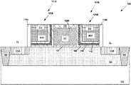
- FIG. 9 depicts the two memory cells 101 A, 101 B (e.g., a dual-bit memory cell).
- the memory cell 101 A comprises a memory gate (MG0) and the memory cell 101 B comprises a memory gate (MG1).
- the combined, merged conductive structure 122 B functions as a shared select gate (SG) for both of the memory cells 101 .
- the doped regions 124 A, 124 B function as, respectively, a source line (SL) and a bit line (BL) for both of the memory cells 101 .
- the dual-bit memory cell may be erased by Fowler-Nordheim (F-N) tunneling or hot-hole injection, and each of the individual memory cells 101 A, 101 B may be programmed separately by source side injection.
- F-N Fowler-Nordheim
- FIG. 10 depicts a bias table for the dual bit memory cell shown in FIG. 9 .
- the novel dual bit memory cell disclosed herein may be arranged in an array having a variety of different configurations.
- FIG. 11 depicts one possible configuration of a memory array wherein all of the dual bit memory cells share a common or local source line.
- FIG. 12 depicts yet another possible configuration of a memory array wherein the source line and the bit line are shared locally between alternating dual bit memory cells.
- the novel, dual bit memory cell disclosed herein is significantly more compact as compared to other memory cells due to the formation of the combined conductive structure 122 B that functions as a shared select gate (SG) for both of the two memory cells 101 A, 101 B.
- the cell size is approximately 0.128 ⁇ m 2 or about 42.2 F 2 .
- the novel arrangement of the compact memory cells 101 shown in FIG. 9 has a cell size of approximately 0.07 ⁇ m 2 or about 23.1 F 2 , which is about 45% less than the cell size of the prior art SONOS cell.
- traditional manufacturing operations may be performed to complete the fabrication of the IC product 100 .
- the novel, dual bit memory cell disclosed herein may come in a variety of configurations where the conductive structure 122 B is a select gate (SG) that is shared by both of the memory cells 101 A and 101 B.
- FIG. 13 depicts an embodiment wherein the conductive material for the conductive structures 122 is deposited and patterned in such a manner that the upper surface of the second conductive structure 122 B (i.e., the shared select gate) is positioned at a level that is above the level of the upper surface of the gate caps 116 .
- a first portion of the second conductive structure 122 B is positioned vertically above a portion of the gate structure 121 A of the memory cell 101 A, while a second portion of the second conductive structure 122 B is positioned vertically above a portion of the gate structure 121 B of the memory cell 101 B.
- the cap layer 116 is positioned above the conductive structure 122 B, i.e., the shared select gate (SG).
- This structure may be achieved by sequentially depositing the materials for the insulation layer 120 , the conductive structures 122 and the capping layer 116 on the product and thereafter patterning those materials by performing known masking and etching techniques. Thereafter, the gate structure 121 A for the memory cell 101 A was formed between the first conductive structure 122 A and the second conductive structure 122 B, and the gate structure 121 B for the memory cell 101 B was formed between the second conductive structure 122 B and the third conductive structure 122 C.
- the materials for the gate insulation layer 108 , the charge storage layer 110 and the blocking insulation layer 112 were formed by performing conformal deposition processes. Thereafter, the gate electrode material 114 was deposited so as to over-fill the remaining spaces between the conductive structures 122 . At that point, the materials for the gate structures were patterned by performing known masking and etching techniques. Thereafter, the first conductive structure 122 A and the third conductive structure 122 C were removed. Note that the uppermost surface of the gate structures 121 is positioned at a level that is above the level of the upper surface of the conductive structure 122 B.
- a portion of the gate structure 121 A of the memory cell 101 A is positioned vertically above a portion of the second conductive structure 122 B and a portion of the gate structure 121 B of the memory cell 101 B is positioned vertically above the second conductive structure 122 B.
- the gate structure 121 A of the memory cell 101 A, and particularly the gate insulation layer 108 is positioned on and in physical contact with the conductive structure 122 B (i.e., the shared select gate (SG)), while the gate structure 121 B of the memory cell 101 B, and particularly the gate insulation layer 108 , is positioned on and in physical contact with the conductive structure 122 B.
- FIG. 15 depicts an embodiment that is similar to the embodiment shown in FIG. 14 , in that the capping material 116 is positioned above the conductive structure 122 B and that the materials for the gate insulation layer 108 , the charge storage layer 110 and the blocking insulation layer 112 were formed by performing conformal deposition processes.
- a CMP process operation was performed to remove all materials above the upper surface of the cap layer 116 .
- the upper surface of the gate structures is substantially co-planar with the upper surface of the cap layer 116 .
- the gate structure 121 A of the memory cell 101 A, and particularly the gate insulation layer 108 is positioned on and in physical contact with the conductive structure 122 B, while the gate structure 121 B of the memory cell 101 B, and particularly the gate insulation layer 108 , is positioned on and in physical contact with the conductive structure 122 B.
Landscapes
- Engineering & Computer Science (AREA)
- Microelectronics & Electronic Packaging (AREA)
- Non-Volatile Memory (AREA)
- Semiconductor Memories (AREA)
Abstract
Description
Claims (20)
Priority Applications (2)
| Application Number | Priority Date | Filing Date | Title |
|---|---|---|---|
| US16/940,586 US11437392B2 (en) | 2020-07-28 | 2020-07-28 | Compact memory cell with a shared conductive select gate and methods of making such a memory cell |
| CN202110850629.5A CN114005874A (en) | 2020-07-28 | 2021-07-27 | Compact memory cell with shared conductive select gate and method of making the same |
Applications Claiming Priority (1)
| Application Number | Priority Date | Filing Date | Title |
|---|---|---|---|
| US16/940,586 US11437392B2 (en) | 2020-07-28 | 2020-07-28 | Compact memory cell with a shared conductive select gate and methods of making such a memory cell |
Publications (2)
| Publication Number | Publication Date |
|---|---|
| US20220037349A1 US20220037349A1 (en) | 2022-02-03 |
| US11437392B2 true US11437392B2 (en) | 2022-09-06 |
Family
ID=79920991
Family Applications (1)
| Application Number | Title | Priority Date | Filing Date |
|---|---|---|---|
| US16/940,586 Active 2040-08-27 US11437392B2 (en) | 2020-07-28 | 2020-07-28 | Compact memory cell with a shared conductive select gate and methods of making such a memory cell |
Country Status (2)
| Country | Link |
|---|---|
| US (1) | US11437392B2 (en) |
| CN (1) | CN114005874A (en) |
Families Citing this family (1)
| Publication number | Priority date | Publication date | Assignee | Title |
|---|---|---|---|---|
| US11437392B2 (en) | 2020-07-28 | 2022-09-06 | Globalfoundries Singapore Pte. Ltd. | Compact memory cell with a shared conductive select gate and methods of making such a memory cell |
Citations (11)
| Publication number | Priority date | Publication date | Assignee | Title |
|---|---|---|---|---|
| US6630383B1 (en) | 2002-09-23 | 2003-10-07 | Advanced Micro Devices, Inc. | Bi-layer floating gate for improved work function between floating gate and a high-K dielectric layer |
| US20070215929A1 (en) | 2006-03-15 | 2007-09-20 | Naoki Yasuda | Nonvolatile semiconductor memory device |
| US20080237696A1 (en) | 2004-07-01 | 2008-10-02 | Chih-Hsin Wang | Alignment protection in non-volatile memory and array |
| US20090016113A1 (en) | 2007-07-10 | 2009-01-15 | Silicon Storage Technology, Inc. | Non-diffusion junction split-gate nonvolatile memory cells and arrays, methods of programming, erasing, and reading thereof, and methods of manufacture |
| US20090140317A1 (en) | 2007-12-03 | 2009-06-04 | Interuniversitair Microelektronica Centrum (Imec) | Multiple Layer floating gate non-volatile memory device |
| US20100173485A1 (en) | 2009-01-07 | 2010-07-08 | Seung-Jun Lee | Method of manufacturing a non-volatile memory device |
| US20150187787A1 (en) * | 2013-12-30 | 2015-07-02 | Globalfoundries Singapore Pte. Ltd. | Multi-level memory cells and methods for forming multi-level memory cells |
| US20170062446A1 (en) | 2015-08-24 | 2017-03-02 | Renesas Electronics Corporation | Semiconductor device and method of manufacturing the same |
| US20200350325A1 (en) | 2019-04-30 | 2020-11-05 | Shanghai Huali Microelectronics Corporation | Semiconductor structure of split gate flash memory cell and method for manufacturing the same |
| CN114005874A (en) | 2020-07-28 | 2022-02-01 | 格芯新加坡私人有限公司 | Compact memory cell with shared conductive select gate and method of making the same |
| CN114005873A (en) | 2020-07-28 | 2022-02-01 | 格芯新加坡私人有限公司 | Compact memory cell with shared conductive word line and method of making the same |
Family Cites Families (21)
| Publication number | Priority date | Publication date | Assignee | Title |
|---|---|---|---|---|
| US6133098A (en) * | 1999-05-17 | 2000-10-17 | Halo Lsi Design & Device Technology, Inc. | Process for making and programming and operating a dual-bit multi-level ballistic flash memory |
| JP4715024B2 (en) * | 2001-05-08 | 2011-07-06 | セイコーエプソン株式会社 | Program method for nonvolatile semiconductor memory device |
| TW583673B (en) * | 2001-07-06 | 2004-04-11 | Halo Lsi Inc | A control gate decoder for twin MONOS memory with two bit erase capability |
| JP2004071646A (en) * | 2002-08-01 | 2004-03-04 | Nec Electronics Corp | Nonvolatile semiconductor memory device and method of manufacturing and controlling the same |
| DE10238784A1 (en) * | 2002-08-23 | 2004-03-11 | Infineon Technologies Ag | Non-volatile semiconductor memory element and associated manufacturing and control method |
| KR100521371B1 (en) * | 2003-01-22 | 2005-10-12 | 삼성전자주식회사 | Silicon-Oxide-Nitride-Oxide-Silicon (SONOS) Type Nonvolatile Memory And Method Of Fabricating The Same |
| JP2004342682A (en) * | 2003-05-13 | 2004-12-02 | Sharp Corp | Semiconductor device and its manufacturing method, portable electronic device, and IC card |
| US7129539B2 (en) * | 2003-05-15 | 2006-10-31 | Sharp Kabushiki Kaisha | Semiconductor storage device and manufacturing method therefor, semiconductor device, portable electronic equipment and IC card |
| TWI235462B (en) * | 2004-07-21 | 2005-07-01 | Powerchip Semiconductor Corp | Nonvolatile memory and manufacturing method thereof |
| JP4902196B2 (en) * | 2005-02-09 | 2012-03-21 | シャープ株式会社 | Nonvolatile semiconductor memory device |
| US7488645B2 (en) * | 2005-04-13 | 2009-02-10 | United Microelectronics Corp. | Method of fabricating a non-volatile memory |
| TWI265626B (en) * | 2005-08-19 | 2006-11-01 | Powerchip Semiconductor Corp | Non-volatile memory and manufacturing method and operating method thereof |
| US7915123B1 (en) * | 2006-04-20 | 2011-03-29 | Spansion Llc | Dual charge storage node memory device and methods for fabricating such device |
| US7557008B2 (en) * | 2007-01-23 | 2009-07-07 | Freescale Semiconductor, Inc. | Method of making a non-volatile memory device |
| US8803217B2 (en) * | 2007-03-13 | 2014-08-12 | Freescale Semiconductor, Inc. | Process of forming an electronic device including a control gate electrode, a semiconductor layer, and a select gate electrode |
| US8785307B2 (en) * | 2012-08-23 | 2014-07-22 | Silicon Storage Technology, Inc. | Method of forming a memory cell by reducing diffusion of dopants under a gate |
| US9257554B2 (en) * | 2013-08-13 | 2016-02-09 | Globalfoundries Singapore Pte. Ltd. | Split gate embedded memory technology and method of manufacturing thereof |
| US9159842B1 (en) * | 2014-03-28 | 2015-10-13 | Taiwan Semiconductor Manufacturing Co., Ltd. | Embedded nonvolatile memory |
| TWI594378B (en) * | 2015-05-04 | 2017-08-01 | 北京芯盈速騰電子科技有限責任公司 | Non-volatile memory cell and manufacture method of the same |
| US9859291B2 (en) * | 2015-08-03 | 2018-01-02 | Iotmemory Technology Inc. | Non-volatile memory and manufacturing method thereof |
| US10658479B2 (en) * | 2017-11-15 | 2020-05-19 | Taiwan Semiconductor Manufacturing Co., Ltd. | Flash memory cell structure with step-shaped floating gate |
-
2020
- 2020-07-28 US US16/940,586 patent/US11437392B2/en active Active
-
2021
- 2021-07-27 CN CN202110850629.5A patent/CN114005874A/en active Pending
Patent Citations (11)
| Publication number | Priority date | Publication date | Assignee | Title |
|---|---|---|---|---|
| US6630383B1 (en) | 2002-09-23 | 2003-10-07 | Advanced Micro Devices, Inc. | Bi-layer floating gate for improved work function between floating gate and a high-K dielectric layer |
| US20080237696A1 (en) | 2004-07-01 | 2008-10-02 | Chih-Hsin Wang | Alignment protection in non-volatile memory and array |
| US20070215929A1 (en) | 2006-03-15 | 2007-09-20 | Naoki Yasuda | Nonvolatile semiconductor memory device |
| US20090016113A1 (en) | 2007-07-10 | 2009-01-15 | Silicon Storage Technology, Inc. | Non-diffusion junction split-gate nonvolatile memory cells and arrays, methods of programming, erasing, and reading thereof, and methods of manufacture |
| US20090140317A1 (en) | 2007-12-03 | 2009-06-04 | Interuniversitair Microelektronica Centrum (Imec) | Multiple Layer floating gate non-volatile memory device |
| US20100173485A1 (en) | 2009-01-07 | 2010-07-08 | Seung-Jun Lee | Method of manufacturing a non-volatile memory device |
| US20150187787A1 (en) * | 2013-12-30 | 2015-07-02 | Globalfoundries Singapore Pte. Ltd. | Multi-level memory cells and methods for forming multi-level memory cells |
| US20170062446A1 (en) | 2015-08-24 | 2017-03-02 | Renesas Electronics Corporation | Semiconductor device and method of manufacturing the same |
| US20200350325A1 (en) | 2019-04-30 | 2020-11-05 | Shanghai Huali Microelectronics Corporation | Semiconductor structure of split gate flash memory cell and method for manufacturing the same |
| CN114005874A (en) | 2020-07-28 | 2022-02-01 | 格芯新加坡私人有限公司 | Compact memory cell with shared conductive select gate and method of making the same |
| CN114005873A (en) | 2020-07-28 | 2022-02-01 | 格芯新加坡私人有限公司 | Compact memory cell with shared conductive word line and method of making the same |
Non-Patent Citations (17)
Also Published As
| Publication number | Publication date |
|---|---|
| CN114005874A (en) | 2022-02-01 |
| US20220037349A1 (en) | 2022-02-03 |
Similar Documents
| Publication | Publication Date | Title |
|---|---|---|
| TWI663715B (en) | String select line gate oxide method for 3d vertical channel nand memory | |
| US7795088B2 (en) | Method for manufacturing memory cell | |
| CN108461395B (en) | Method for manufacturing semiconductor device | |
| US20200350213A1 (en) | Embedded sonos and high voltage select gate with a high-k metal gate and manufacturing methods of the same | |
| US8803220B2 (en) | P-type control gate in non-volatile storage | |
| WO2011160011A1 (en) | Isolation between nonvolatile memory cells by means of low- dielectric- constant dielectrics and air gaps and corresponding manufacturing method | |
| US9230971B2 (en) | NAND string containing self-aligned control gate sidewall cladding | |
| US20170117372A1 (en) | Semiconductor device and method of fabricating semiconductor device | |
| US11678491B2 (en) | Embedded memory using SOI structures and methods | |
| US20040238878A1 (en) | Manufacturing method of a semiconductor integrated circuit device | |
| US11101281B2 (en) | Semiconductor device and method of manufacturing the same | |
| US20140367766A1 (en) | Nonvolatile semiconductor storage device and method of manufacture thereof | |
| US20120286349A1 (en) | Non-Volatile Memory Device With Additional Conductive Storage Layer | |
| CN107731827A (en) | Flash memory device | |
| US9935119B2 (en) | Dual control gate spacer structure for embedded flash memory | |
| US6448126B1 (en) | Method of forming an embedded memory | |
| US20230067382A1 (en) | Integrated chip with a gate structure disposed within a trench | |
| US7842993B2 (en) | Nonvolatile semiconductor memory device suppressing fluctuation in threshold voltage | |
| US11437392B2 (en) | Compact memory cell with a shared conductive select gate and methods of making such a memory cell | |
| CN101388416B (en) | Nonvolatile semiconductor storage device and manufacturing method thereof | |
| US11309324B2 (en) | Compact memory cell with a shared conductive word line and methods of making such a memory cell | |
| US20080123433A1 (en) | Flash memory device and method of manufacturing the same | |
| US20110175155A1 (en) | Nonvolatile semiconductor memory device | |
| US20250344394A1 (en) | Nand flash memory and manufacturing method thereof | |
| KR101983682B1 (en) | Edge rounded field effect transistors and methods of manufacturing |
Legal Events
| Date | Code | Title | Description |
|---|---|---|---|
| AS | Assignment |
Owner name: GLOBALFOUNDRIES SINGAPORE PTE LTD, SINGAPORE Free format text: ASSIGNMENT OF ASSIGNORS INTEREST;ASSIGNORS:SUN, YONGSHUN;TOH, ENG HUAT;TAN, SHYUE SENG;AND OTHERS;REEL/FRAME:053326/0799 Effective date: 20200728 |
|
| FEPP | Fee payment procedure |
Free format text: ENTITY STATUS SET TO UNDISCOUNTED (ORIGINAL EVENT CODE: BIG.); ENTITY STATUS OF PATENT OWNER: LARGE ENTITY |
|
| STPP | Information on status: patent application and granting procedure in general |
Free format text: RESPONSE TO NON-FINAL OFFICE ACTION ENTERED AND FORWARDED TO EXAMINER |
|
| STPP | Information on status: patent application and granting procedure in general |
Free format text: NOTICE OF ALLOWANCE MAILED -- APPLICATION RECEIVED IN OFFICE OF PUBLICATIONS |
|
| STPP | Information on status: patent application and granting procedure in general |
Free format text: AWAITING TC RESP., ISSUE FEE NOT PAID |
|
| STPP | Information on status: patent application and granting procedure in general |
Free format text: NOTICE OF ALLOWANCE MAILED -- APPLICATION RECEIVED IN OFFICE OF PUBLICATIONS |
|
| STPP | Information on status: patent application and granting procedure in general |
Free format text: PUBLICATIONS -- ISSUE FEE PAYMENT VERIFIED |
|
| STCF | Information on status: patent grant |
Free format text: PATENTED CASE |
|
| MAFP | Maintenance fee payment |
Free format text: PAYMENT OF MAINTENANCE FEE, 4TH YEAR, LARGE ENTITY (ORIGINAL EVENT CODE: M1551); ENTITY STATUS OF PATENT OWNER: LARGE ENTITY Year of fee payment: 4 |