US11430965B2 - Organic light emitting diode and organic light emitting display device including the same - Google Patents
Organic light emitting diode and organic light emitting display device including the same Download PDFInfo
- Publication number
- US11430965B2 US11430965B2 US16/701,611 US201916701611A US11430965B2 US 11430965 B2 US11430965 B2 US 11430965B2 US 201916701611 A US201916701611 A US 201916701611A US 11430965 B2 US11430965 B2 US 11430965B2
- Authority
- US
- United States
- Prior art keywords
- layer
- charge generation
- organic light
- light emitting
- organic
- Prior art date
- Legal status (The legal status is an assumption and is not a legal conclusion. Google has not performed a legal analysis and makes no representation as to the accuracy of the status listed.)
- Active, expires
Links
Images


Classifications
-
- H—ELECTRICITY
- H10—SEMICONDUCTOR DEVICES; ELECTRIC SOLID-STATE DEVICES NOT OTHERWISE PROVIDED FOR
- H10K—ORGANIC ELECTRIC SOLID-STATE DEVICES
- H10K50/00—Organic light-emitting devices
- H10K50/10—OLEDs or polymer light-emitting diodes [PLED]
- H10K50/19—Tandem OLEDs
-
- H—ELECTRICITY
- H10—SEMICONDUCTOR DEVICES; ELECTRIC SOLID-STATE DEVICES NOT OTHERWISE PROVIDED FOR
- H10K—ORGANIC ELECTRIC SOLID-STATE DEVICES
- H10K50/00—Organic light-emitting devices
- H10K50/10—OLEDs or polymer light-emitting diodes [PLED]
- H10K50/11—OLEDs or polymer light-emitting diodes [PLED] characterised by the electroluminescent [EL] layers
- H10K50/125—OLEDs or polymer light-emitting diodes [PLED] characterised by the electroluminescent [EL] layers specially adapted for multicolour light emission, e.g. for emitting white light
- H10K50/13—OLEDs or polymer light-emitting diodes [PLED] characterised by the electroluminescent [EL] layers specially adapted for multicolour light emission, e.g. for emitting white light comprising stacked EL layers within one EL unit
- H10K50/131—OLEDs or polymer light-emitting diodes [PLED] characterised by the electroluminescent [EL] layers specially adapted for multicolour light emission, e.g. for emitting white light comprising stacked EL layers within one EL unit with spacer layers between the electroluminescent layers
-
- H01L51/504—
-
- H01L51/0067—
-
- H01L51/0072—
-
- H01L51/0073—
-
- H01L51/5004—
-
- H—ELECTRICITY
- H10—SEMICONDUCTOR DEVICES; ELECTRIC SOLID-STATE DEVICES NOT OTHERWISE PROVIDED FOR
- H10K—ORGANIC ELECTRIC SOLID-STATE DEVICES
- H10K50/00—Organic light-emitting devices
- H10K50/10—OLEDs or polymer light-emitting diodes [PLED]
- H10K50/11—OLEDs or polymer light-emitting diodes [PLED] characterised by the electroluminescent [EL] layers
- H10K50/12—OLEDs or polymer light-emitting diodes [PLED] characterised by the electroluminescent [EL] layers comprising dopants
-
- H—ELECTRICITY
- H10—SEMICONDUCTOR DEVICES; ELECTRIC SOLID-STATE DEVICES NOT OTHERWISE PROVIDED FOR
- H10K—ORGANIC ELECTRIC SOLID-STATE DEVICES
- H10K50/00—Organic light-emitting devices
- H10K50/10—OLEDs or polymer light-emitting diodes [PLED]
- H10K50/11—OLEDs or polymer light-emitting diodes [PLED] characterised by the electroluminescent [EL] layers
- H10K50/125—OLEDs or polymer light-emitting diodes [PLED] characterised by the electroluminescent [EL] layers specially adapted for multicolour light emission, e.g. for emitting white light
- H10K50/13—OLEDs or polymer light-emitting diodes [PLED] characterised by the electroluminescent [EL] layers specially adapted for multicolour light emission, e.g. for emitting white light comprising stacked EL layers within one EL unit
-
- H—ELECTRICITY
- H10—SEMICONDUCTOR DEVICES; ELECTRIC SOLID-STATE DEVICES NOT OTHERWISE PROVIDED FOR
- H10K—ORGANIC ELECTRIC SOLID-STATE DEVICES
- H10K59/00—Integrated devices, or assemblies of multiple devices, comprising at least one organic light-emitting element covered by group H10K50/00
- H10K59/30—Devices specially adapted for multicolour light emission
- H10K59/35—Devices specially adapted for multicolour light emission comprising red-green-blue [RGB] subpixels
- H10K59/351—Devices specially adapted for multicolour light emission comprising red-green-blue [RGB] subpixels comprising more than three subpixels, e.g. red-green-blue-white [RGBW]
-
- H—ELECTRICITY
- H10—SEMICONDUCTOR DEVICES; ELECTRIC SOLID-STATE DEVICES NOT OTHERWISE PROVIDED FOR
- H10K—ORGANIC ELECTRIC SOLID-STATE DEVICES
- H10K85/00—Organic materials used in the body or electrodes of devices covered by this subclass
- H10K85/60—Organic compounds having low molecular weight
- H10K85/649—Aromatic compounds comprising a hetero atom
- H10K85/654—Aromatic compounds comprising a hetero atom comprising only nitrogen as heteroatom
-
- H—ELECTRICITY
- H10—SEMICONDUCTOR DEVICES; ELECTRIC SOLID-STATE DEVICES NOT OTHERWISE PROVIDED FOR
- H10K—ORGANIC ELECTRIC SOLID-STATE DEVICES
- H10K85/00—Organic materials used in the body or electrodes of devices covered by this subclass
- H10K85/60—Organic compounds having low molecular weight
- H10K85/649—Aromatic compounds comprising a hetero atom
- H10K85/657—Polycyclic condensed heteroaromatic hydrocarbons
- H10K85/6572—Polycyclic condensed heteroaromatic hydrocarbons comprising only nitrogen in the heteroaromatic polycondensed ring system, e.g. phenanthroline or carbazole
-
- H—ELECTRICITY
- H10—SEMICONDUCTOR DEVICES; ELECTRIC SOLID-STATE DEVICES NOT OTHERWISE PROVIDED FOR
- H10K—ORGANIC ELECTRIC SOLID-STATE DEVICES
- H10K85/00—Organic materials used in the body or electrodes of devices covered by this subclass
- H10K85/60—Organic compounds having low molecular weight
- H10K85/649—Aromatic compounds comprising a hetero atom
- H10K85/657—Polycyclic condensed heteroaromatic hydrocarbons
- H10K85/6574—Polycyclic condensed heteroaromatic hydrocarbons comprising only oxygen in the heteroaromatic polycondensed ring system, e.g. cumarine dyes
-
- H01L2251/303—
-
- H01L2251/5307—
-
- H01L2251/5315—
-
- H01L2251/552—
-
- H01L2251/558—
-
- H01L27/3244—
-
- H01L51/5056—
-
- H01L51/5072—
-
- H01L51/5088—
-
- H01L51/5092—
-
- H01L51/5096—
-
- H—ELECTRICITY
- H10—SEMICONDUCTOR DEVICES; ELECTRIC SOLID-STATE DEVICES NOT OTHERWISE PROVIDED FOR
- H10K—ORGANIC ELECTRIC SOLID-STATE DEVICES
- H10K2101/00—Properties of the organic materials covered by group H10K85/00
- H10K2101/30—Highest occupied molecular orbital [HOMO], lowest unoccupied molecular orbital [LUMO] or Fermi energy values
-
- H—ELECTRICITY
- H10—SEMICONDUCTOR DEVICES; ELECTRIC SOLID-STATE DEVICES NOT OTHERWISE PROVIDED FOR
- H10K—ORGANIC ELECTRIC SOLID-STATE DEVICES
- H10K2101/00—Properties of the organic materials covered by group H10K85/00
- H10K2101/40—Interrelation of parameters between multiple constituent active layers or sublayers, e.g. HOMO values in adjacent layers
-
- H—ELECTRICITY
- H10—SEMICONDUCTOR DEVICES; ELECTRIC SOLID-STATE DEVICES NOT OTHERWISE PROVIDED FOR
- H10K—ORGANIC ELECTRIC SOLID-STATE DEVICES
- H10K2102/00—Constructional details relating to the organic devices covered by this subclass
-
- H—ELECTRICITY
- H10—SEMICONDUCTOR DEVICES; ELECTRIC SOLID-STATE DEVICES NOT OTHERWISE PROVIDED FOR
- H10K—ORGANIC ELECTRIC SOLID-STATE DEVICES
- H10K2102/00—Constructional details relating to the organic devices covered by this subclass
- H10K2102/301—Details of OLEDs
- H10K2102/302—Details of OLEDs of OLED structures
- H10K2102/3023—Direction of light emission
- H10K2102/3026—Top emission
-
- H—ELECTRICITY
- H10—SEMICONDUCTOR DEVICES; ELECTRIC SOLID-STATE DEVICES NOT OTHERWISE PROVIDED FOR
- H10K—ORGANIC ELECTRIC SOLID-STATE DEVICES
- H10K2102/00—Constructional details relating to the organic devices covered by this subclass
- H10K2102/301—Details of OLEDs
- H10K2102/351—Thickness
-
- H—ELECTRICITY
- H10—SEMICONDUCTOR DEVICES; ELECTRIC SOLID-STATE DEVICES NOT OTHERWISE PROVIDED FOR
- H10K—ORGANIC ELECTRIC SOLID-STATE DEVICES
- H10K50/00—Organic light-emitting devices
- H10K50/10—OLEDs or polymer light-emitting diodes [PLED]
- H10K50/14—Carrier transporting layers
- H10K50/15—Hole transporting layers
-
- H—ELECTRICITY
- H10—SEMICONDUCTOR DEVICES; ELECTRIC SOLID-STATE DEVICES NOT OTHERWISE PROVIDED FOR
- H10K—ORGANIC ELECTRIC SOLID-STATE DEVICES
- H10K50/00—Organic light-emitting devices
- H10K50/10—OLEDs or polymer light-emitting diodes [PLED]
- H10K50/14—Carrier transporting layers
- H10K50/16—Electron transporting layers
-
- H—ELECTRICITY
- H10—SEMICONDUCTOR DEVICES; ELECTRIC SOLID-STATE DEVICES NOT OTHERWISE PROVIDED FOR
- H10K—ORGANIC ELECTRIC SOLID-STATE DEVICES
- H10K50/00—Organic light-emitting devices
- H10K50/10—OLEDs or polymer light-emitting diodes [PLED]
- H10K50/17—Carrier injection layers
-
- H—ELECTRICITY
- H10—SEMICONDUCTOR DEVICES; ELECTRIC SOLID-STATE DEVICES NOT OTHERWISE PROVIDED FOR
- H10K—ORGANIC ELECTRIC SOLID-STATE DEVICES
- H10K50/00—Organic light-emitting devices
- H10K50/10—OLEDs or polymer light-emitting diodes [PLED]
- H10K50/17—Carrier injection layers
- H10K50/171—Electron injection layers
-
- H—ELECTRICITY
- H10—SEMICONDUCTOR DEVICES; ELECTRIC SOLID-STATE DEVICES NOT OTHERWISE PROVIDED FOR
- H10K—ORGANIC ELECTRIC SOLID-STATE DEVICES
- H10K50/00—Organic light-emitting devices
- H10K50/10—OLEDs or polymer light-emitting diodes [PLED]
- H10K50/18—Carrier blocking layers
-
- H—ELECTRICITY
- H10—SEMICONDUCTOR DEVICES; ELECTRIC SOLID-STATE DEVICES NOT OTHERWISE PROVIDED FOR
- H10K—ORGANIC ELECTRIC SOLID-STATE DEVICES
- H10K50/00—Organic light-emitting devices
- H10K50/10—OLEDs or polymer light-emitting diodes [PLED]
- H10K50/18—Carrier blocking layers
- H10K50/181—Electron blocking layers
-
- H—ELECTRICITY
- H10—SEMICONDUCTOR DEVICES; ELECTRIC SOLID-STATE DEVICES NOT OTHERWISE PROVIDED FOR
- H10K—ORGANIC ELECTRIC SOLID-STATE DEVICES
- H10K59/00—Integrated devices, or assemblies of multiple devices, comprising at least one organic light-emitting element covered by group H10K50/00
- H10K59/10—OLED displays
- H10K59/12—Active-matrix OLED [AMOLED] displays
- H10K59/131—Interconnections, e.g. wiring lines or terminals
Definitions
- the present disclosure relates to an organic light emitting diode, and more particularly, to an organic light emitting diode (OLED) having high emitting efficiency and long lifespan and an organic light emitting display device including the same.
- OLED organic light emitting diode
- the OLED emits light by injecting electrons from a cathode as an electron injection electrode and holes from an anode as a hole injection electrode into an organic emitting layer, combining the electrons with the holes, generating an exciton, and transforming the exciton from an excited state to a ground state.
- a flexible transparent substrate for example, a plastic substrate, can be used as a base substrate where elements are formed.
- the OLED can be operated at a voltage (e.g., 10V or below) lower than a voltage required to operate other display devices and has low power consumption.
- the light from the OLED has excellent color purity.
- the OLED may include a first electrode, which is formed over a substrate and acts as an anode, a second electrode, which faces the first electrode and acts as a cathode, and an organic emitting layer therebetween.
- an organic light emitting display device which includes an OLED, which emits white light in a red pixel, a green pixel and a blue pixel, and a color filter, is introduced.
- the light emitting diode may be called as a white organic light emitting diode (W-OLED).
- the above W-OLED has a stack structure which includes at least two emitting parts. However, a driving voltage of the stack structure W-OLED is increased, and a lifespan of the stack structure W-OLED is decreased.
- embodiments of the present disclosure are directed to an organic light emitting diode and an organic light emitting display device including the same that substantially obviate one or more of the problems due to limitations and disadvantages of the related art.
- an organic light emitting diode comprises a first electrode; a second electrode facing the first electrode; and an organic emitting layer between the first and second electrodes, wherein the organic emitting layer includes a first emitting part between the first and second electrodes, a second emitting part between the first emitting part and the second electrode, and a charge generation layer between the first emitting part and the second emitting part; wherein the charge generation layer includes an n-type charge generation layer between the first emitting part and the second emitting part, and a p-type charge generation layer between the n-type charge generation layer and the second emitting part, and wherein the p-type charge generation layer has a multi-layered structure, where an organic charge generation material layer and an inorganic charge generation material layer are alternately stacked.
- an organic light emitting diode comprises a first electrode; a second electrode facing the first electrode; and an organic emitting layer between the first and second electrodes; wherein the organic emitting layer includes a multi-stack structure comprising a plurality of emitting parts, and a charge generation layer between the adjacent emitting parts; wherein the charge generation layer includes an n-type charge generation layer and a p-type charge generation layer; wherein the p-type charge generation layer includes first and second layers and a third layer between the first and second layers, and wherein each of the first and second layers includes one of organic charge generation material and inorganic charge generation material, and the third layer includes the other one of organic charge generation material and inorganic charge generation material.
- an organic light emitting display device comprises a substrate; and an organic light emitting diode over the substrate, the organic light emitting diode including: a first electrode; a second electrode facing the first electrode; and an organic emitting layer between the first and second electrodes, wherein the organic emitting layer includes a first emitting part between the first and second electrodes, a second emitting part between the first emitting part and the second electrode, and a charge generation layer between the first emitting part and the second emitting part; wherein the charge generation layer includes an n-type charge generation layer between the first emitting part and the second emitting part, and a p-type charge generation layer between the n-type charge generation layer and the second emitting part, and wherein the p-type charge generation layer has a multi-layered structure, where an organic charge generation material layer and an inorganic charge generation material layer are alternately stacked.
- an organic light emitting display device comprises a substrate; and an organic light emitting diode over the substrate, the organic light emitting diode including: a first electrode; a second electrode facing the first electrode; and an organic emitting layer between the first and second electrodes; wherein the organic emitting layer includes a multi-stack structure comprising a plurality of emitting parts, and a charge generation layer between the adjacent emitting parts; wherein the charge generation layer includes an n-type charge generation layer and a p-type charge generation layer; wherein the p-type charge generation layer includes first and second layers and a third layer between the first and second layers, and wherein each of the first and second layers includes one of organic charge generation material and inorganic charge generation material, and the third layer includes the other one of organic charge generation material and inorganic charge generation material.
- FIG. 1 is a schematic circuit diagram of an organic light emitting display device according to the present disclosure.
- FIG. 2 is a schematic cross-sectional view of an OLED according to a first embodiment of the present disclosure.
- FIGS. 3A and 3B are schematic cross-sectional views illustrating a p-type charge generation layer, respectively.
- FIG. 4 is a schematic cross-sectional view of an organic light emitting display device according to a second embodiment of the present disclosure.
- FIG. 5 is a schematic cross-sectional view of an organic light emitting display device according to a third embodiment of the present disclosure.
- FIG. 1 is a schematic circuit diagram of an organic light emitting display device according to the present disclosure.
- a gate line GL, a data line DL and a power line PL are formed, and a pixel region P is defined by the gate and data lines GL and DL.
- a switching thin film transistor (TFT) Ts, a driving TFT Td, a storage capacitor Cst and an organic light emitting diode (OLED) D are formed.
- the switching TFT Ts is connected to the gate line GL and the data line DL, and the driving TFT Td and the storage capacitor Cst are connected to the switching TFT Ts and the power line PL.
- the OLED D is connected to the driving TFT Td.
- the switching TFT Ts when the switching TFT Ts is turned on by a gate signal applied through the gate line GL, a data signal from the data line DL is applied to a gate electrode of the driving TFT Td and an electrode of the storage capacitor Cst through the switching TFT Ts.
- the driving TFT Td When the driving TFT Td is turned on by the data signal, an electric current is supplied to the OLED D from the power line PL through the driving TFT Td. As a result, the OLED D emits light.
- the storage capacitor Cst serves to maintain the voltage of the gate electrode of the driving TFT Td for one frame. Accordingly, the organic light emitting display device displays images.
- FIG. 2 is a schematic cross-sectional view of an OLED according to a first embodiment of the present disclosure
- FIGS. 3A and 3B are schematic cross-sectional views illustrating a p-type charge generation layer, respectively.
- the OLED D includes a first electrode 110 , a second electrode 114 facing the first electrode 110 and an organic emitting layer 112 between the first and second electrodes 110 and 114 .
- the first electrode 110 may include a conductive material having a relatively high work function to serve as an anode.
- the first electrode 110 may be formed of a transparent conductive material such as indium-tin-oxide (ITO) or indium-zinc-oxide (IZO).
- the second electrode 114 may cover a display area of an organic light emitting display device and may include a conductive material having a relatively low work function to serve as a cathode.
- the second electrode 114 may be formed of aluminum (Al), magnesium (Mg) or Al—Mg alloy.
- the light from the organic emitting layer 112 may be displayed through the first electrode 110 .
- the OLED D may be a bottom-emission type.
- the organic emitting layer 112 includes a first emitting part 120 between the first and second electrodes 110 and 114 , a second emitting part 130 between the first emitting part 120 and the second electrode 114 and a charge generation layer (CGL) 140 between the first emitting part 120 and the second emitting part 130 .
- the organic emitting layer 112 has a multi-stack structure.
- the CGL 140 is positioned between the first and second emitting parts 120 and 130 and provides an electron into the first emitting part 120 and a hole into the second emitting part 130 .
- the first emitting part 120 includes a first emitting material layer (EML) 126 .
- EML first emitting material layer
- the first EML 126 may include a host and a blue dopant to emit blue light.
- the first emitting part 120 may further include a hole injection layer (HIL) 122 between the first electrode 110 and the first EML 126 , a first hole transporting layer (HTL) 124 between the HIL 122 and the first EML 126 and a first electron transporting layer 128 between the first EML 126 and the CGL 140 .
- the first emitting part 120 may include the first EML 126 , a first hole auxiliary layer between the first electrode 110 and the first EML 126 and including the HIL 122 and the first HTL 124 and a first electron auxiliary layer between the first EML 126 and the CGL 140 and including the first ETL 128 .
- the first emitting part 120 may further include an electron blocking layer between the first HTL 124 and the first EML 126 and a hole blocking layer between the first EML 126 and the first ETL 128 .
- the second emitting part 130 includes a second EML 134 .
- the second EML 134 may include a host and a yellow-green dopant to emit yellow-green light.
- the first EML 126 may emit yellow-green light
- the second EML 134 may emit blue light.
- the blue light or the yellow-green light from the first emitting part 120 and the yellow-green light or the blue light from the second emitting part 130 are mixed such that the OLED emits white light.
- the second emitting part 130 may further include a second HTL 132 between the CGL 140 and the second EML 134 , a second ETL 136 between the second EML 134 and the second electrode 114 and an electron injection layer (EIL) 138 between the second ETL 136 and the second electrode 114 .
- the second emitting part 130 may include the second EML 134 , a second hole auxiliary layer between the CGL 140 and the second EML 134 and including the second HTL 132 and a second electron auxiliary layer between the second EML 134 and the second electrode 114 and including the second ETL 136 and the EIL 138 .
- a thickness of the first HTL 124 may be larger than that of the second HTL 132 , and a thickness of the first ETL 128 may be smaller than that of the second ETL 136 .
- the first HTL 124 may have a thickness of about 500 to 1500 ⁇
- the second HTL 132 may have a thickness of about 100 to 300 ⁇
- the first ETL 128 may have a thickness of about 100 to 300 ⁇
- the second ETL 136 may have a thickness of about 300 to 400 ⁇ .
- the electron injection property from the CGL 140 into the first emitting part 120 and the hole injection property from the CGL 140 into the second emitting part 130 are improved.
- the CGL 140 includes an n-type CGL 142 between the first emitting part 120 and the second emitting part 130 and a p-type CGL 144 between the n-type CGL 142 and the second emitting part 130 .
- the p-type CGL 144 has a triple-layered structure including at least one layer, which is formed of an organic charge generation material, and at least one layer, which is formed of an inorganic charge generation material.
- the p-type CGL 144 includes first and second layers 146 and 147 and a third layer 148 between the first and second layers 146 and 147 .
- Each of the first and second layers 146 and 147 includes one of the organic charge generation material and the inorganic charge generation material
- the third layer 148 includes the other one of the organic charge generation material and the inorganic charge generation material.
- the inorganic charge generation material may be a metal oxide and may have a conduction band level of about 4.0 to 7.5 eV.
- the inorganic charge generation material may be one of WO 3 , MoO 3 , Be 2 O 3 and V 2 O 5 .
- the driving voltage of the OLED is increased. Accordingly, when the p-type CGL 144 is formed of only organic charge generation material, the organic charge generation material is thermally degraded such that the emitting efficiency and the lifespan of the OLED are decreased. Particularly, when the blue EML includes a delayed fluorescent dopant to increase the emitting efficiency, the thermal degradation problem of the organic charge generation material is strongly generated.
- the p-type CGL 144 has a multi-layered structure, where an organic charge generation material layer and an inorganic charge generation material layer are alternately stacked, both the thermal degradation problem by the organic charge generation material and the color shift problem by the inorganic charge generation material are prevented or minimized.
- each of the first and second layers 146 and 147 includes the organic charge generation material
- the third layer 148 includes the inorganic charge generation material
- the organic charge generation material may be the HATCN compound
- the inorganic charge generation material may be the metal oxide, e.g., WO 3 , MoO 3 , Be 2 O 3 or V 2 O 5 .
- the first and second layers 146 and 147 may have a first thickness t 1 and a second thickness t 2 , respectively, and the third layer 148 may have a third thickness t 3 being equal to or greater than each of the first thickness t 1 and the second thickness t 2 .
- each of the first thickness t 1 and the second thickness t 2 may have a range of about 10 to 30 ⁇
- the third thickness t 3 may have a range of about 30 to 80 ⁇ .
- the first and second layers 146 and 147 may include the same material or different material and may have the same thickness or different thicknesses.
- each of the first and second layers 146 and 147 includes the inorganic charge generation material
- the third layer 148 includes the organic charge generation material
- the organic charge generation material may be the HATCN compound
- the inorganic charge generation material may be the metal oxide, e.g., WO 3 , MoO 3 , Be 2 O 3 or V 2 O 5 .
- each of the first thickness t 1 and the second thickness may have a range of about 30 to 80 ⁇
- the third thickness t 3 may have a range of about 10 to 30 ⁇ .
- the first and second layers 146 and 147 may include the same material or different material and may have the same thickness or different thicknesses.
- the electron injection into the first EML 126 which may include a delayed fluorescent host and a delayed fluorescent dopant to serve as a blue EML, is too rich such that a problem of transporting the electron into the first HTL 124 may be generated.
- an electron blocking layer (EBL) including an electron blocking material may be formed between the first EML 126 and the first HTL 124 .
- a difference of a HOMO level of the delayed fluorescent host (HOMO TH ) and a HOMO level of the electron blocking material (HOMO EBM ) may be smaller than 0.3 eV
- a difference of an LUMO level of the delayed fluorescent host (LUMO TH ) and an LUMO level of the electron blocking material (LUMO EBM ) may be equal to or greater than 0.3 eV.
- the delayed fluorescent host may be represented by Formula 1.
- each of A and B is independently selected from the group consisting of substituted or non-substituted dibenzofuranyl, substituted or non-substituted dibenzofuranyl phenyl, substituted or non-substituted carbazolyl and substituted or non-substituted carbazolyl phenyl.
- the substituent may be a cyano group.
- At least one of A and B may be substituted or non-substituted dibenzofuranyl.
- a dibenzofuranyl substituent is bonded (combined) to at least one of a 4 th position or a 6 th position of the dibenzofuran core.
- the delayed fluorescent dopant may be selected from compounds in Formula 2.
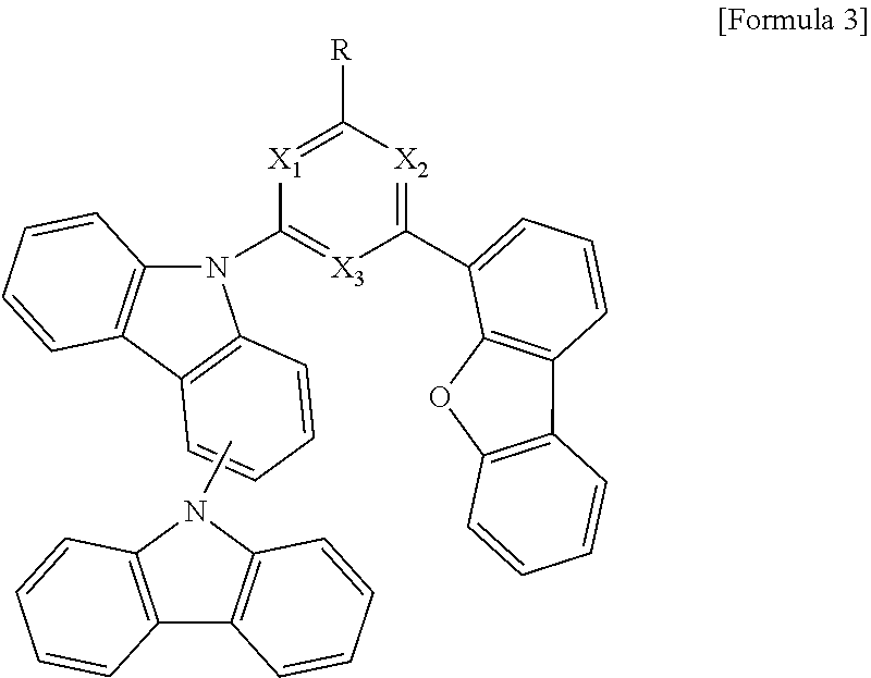
- the electron blocking material may be represented by Formula 3.
- each of X 1 to X 3 is selected from carbon and nitrogen, and at least one of X 1 to X 3 is nitrogen.
- at least one of X 1 to X 3 is nitrogen.
- two of X 1 to X 3 may be nitrogen.
- R is C6 to C30 aryl group.
- the electron blocking material may be selected from compounds in Formula 4.
- an energy level of triplet state of the delayed fluorescent host may be equal to or greater than an energy level of triplet state of the delayed fluorescent dopant (T1 TD ) and may be equal to or smaller than an energy level of triplet state of the electron blocking material (T1 EBL ).
- T1 TD ⁇ T1 TH ⁇ T1 EBL the energy level of triplet state of the delayed fluorescent host (T1 TH ) may be greater than the energy level of triplet state of the delayed fluorescent dopant (T1 TD ) and may be smaller than the energy level of triplet state of the electron blocking material (T1 EBL ).
- the OLED D has a double-stack structure including the first emitting part 120 emitting blue light and the second emitting part 130 emitting yellow-green light.
- the OLED D may has a triple-stack structure including a first emitting part emitting blue light, a second emitting part emitting green light and a third emitting part emitting red light.
- HIL HTCN, 50 ⁇
- HTL HTL
- TCTA HTL
- EBL EBL
- TCTA EBL
- blue EML host (Formula 7): dopant (Formula 8, 30 wt %), 250 ⁇ ), (e) HBL (Formula 9, 100 ⁇ ), (f) first ETL (Formula 10, 100 ⁇ ), (g) n-type CGL (bephene (Formula 11): Li (2 wt %), 100 ⁇ ), (h) p-type CGL (100 ⁇ ), (i) second HTL ( ⁇ -NPB, 100 ⁇ ), (j) yellow-green EML (host (Formula 12): dopant (Formula 13, 5 wt %), 300 ⁇ ), (k) second ETL (Formula 10, 300 ⁇ ), (l) EIL (LiF, 5 ⁇ ), and (
- HATCN compound is used to form the p-type CGL.
- the p-type CGL in the OLED has the HATCN/WO 3 /HATCN structure or the WO 3 /HATCN/WO 3 structure, the brightness, the emitting efficiency and the lifespan of the OLED are improved.
- Example 5 and Example 8 when the WO 3 layer has a thickness being equal to or greater than the HATCN layer, the emitting efficiency and the lifespan of the OLED are further improved.
- the thickness of the WO 3 layer may be greater than that of the HATCN layer.
- FIG. 4 is a schematic cross-sectional view of an organic light emitting display device according to a second embodiment of the present disclosure.
- the organic light emitting display device 100 includes a substrate 150 , a thin film transistor (TFT) Td on the substrate 150 and the OLED D connected to the TFT Td.
- TFT thin film transistor
- the substrate 150 may be a glass substrate or a flexible substrate of polyimide.
- the substrate 150 may have a flexible property.
- a buffer layer of an inorganic material e.g., silicon oxide or silicon nitride, may be formed on the substrate 150 .
- the TFT Td is connected to the switching TFT Ts (of FIG. 1 ) and includes a semiconductor layer 152 , a gate electrode 160 , a source electrode 170 and a drain electrode 172 .
- the semiconductor layer 152 is formed on the substrate 150 .
- the semiconductor layer 152 may be formed of an oxide semiconductor material or a poly-silicon.
- a light-shielding pattern (not shown) may be formed under the semiconductor layer 152 .
- the light to the semiconductor layer 152 is shielded or blocked by the light-shielding pattern such that thermal degradation of the semiconductor layer 152 can be prevented.
- impurities may be doped into both sides of the semiconductor layer 152 .
- a gate insulating layer 154 is formed on the semiconductor layer 152 .
- the gate insulating layer 154 may be formed of an inorganic insulating material such as silicon oxide or silicon nitride.
- a gate electrode 160 which is formed of a conductive material, e.g., metal, is formed on the gate insulating layer 154 to correspond to a center of the semiconductor layer 152 .
- the gate electrode 160 is connected to the switching TFT Ts.
- the gate insulating layer 154 is formed on the entire surface of the substrate 150 .
- the gate insulating layer 154 may be patterned to have the same shape as the gate electrode 160 .
- An interlayer insulating layer 162 which is formed of an insulating material, is formed on an entire surface of the substrate 150 including the gate electrode 160 .
- the interlayer insulating layer 162 may be formed of an inorganic insulating material, e.g., silicon oxide or silicon nitride, or an organic insulating material, e.g., benzocyclobutene or photo-acryl.
- the interlayer insulating layer 162 includes first and second contact holes 166 and 164 exposing both sides of the semiconductor layer 152 .
- the first and second contact holes 166 and 164 are positioned at both sides of the gate electrode 160 to be spaced apart from the gate electrode 160 .
- the first and second contact holes 166 and 164 extend into the gate insulating layer 154 .
- the gate insulating layer 154 is patterned to have the same shape as the gate electrode 160 , there may be no first and second contact holes 166 and 164 in the gate insulating layer 154 .
- a source electrode 170 and a drain electrode 172 which are formed of a conductive material, e.g., metal, are formed on the interlayer insulating layer 162 .
- the source electrode 170 and the drain electrode 172 are spaced apart from each other with respect to the gate electrode 160 and respectively contact both sides of the semiconductor layer 152 through the first and second contact holes 166 and 164 .
- the source electrode 170 is connected to the power line PL ( FIG. 1 ).
- the TFT Td including the semiconductor layer 152 , the gate electrode 160 , the source electrode 170 and the drain electrode 172 serves as a driving element.
- the gate electrode 160 , the source electrode 170 and the drain electrode 172 are positioned over the semiconductor layer 152 .
- the TFT Td has a coplanar structure.
- the gate electrode may be positioned under the semiconductor layer, and the source and drain electrodes may be positioned over the semiconductor layer such that the TFT Td may have an inverted staggered structure.
- the semiconductor layer may include amorphous silicon.
- the switching TFT Ts may have substantially same structure as the TFT Td.
- a passivation layer 174 which includes a drain contact hole 176 exposing the drain electrode 172 of the TFT Td, is formed to cover the TFT Td.
- the OLED D including the first electrode 110 , the organic emitting layer 112 and the second electrode 114 is formed on the passivation layer 174 and over the substrate 150 .
- the first electrode 110 which is connected to the drain electrode 172 of the TFT Td through the drain contact hole 176 , is separately formed on the passivation layer 174 in each pixel region.
- the first electrode 110 may be an anode and may be formed of a conductive material having a relatively high work function.
- the first electrode 110 may be formed of a transparent conductive material such as indium-tin-oxide (ITO) or indium-zinc-oxide (IZO).
- a bank layer 115 which covers edges of the first electrode 110 , is formed on the passivation layer 174 .
- the bank 115 exposes a center of the first electrode 110 in the pixel region.
- the organic emitting layer 112 is formed on the first electrode 110 .
- the organic emitting layer 112 includes the first emitting part 120 between the first and second electrodes 110 and 114 , the second emitting part 130 between the first emitting part 120 and the second electrode 114 and the CGL 140 between the first and second emitting parts 120 and 130 .
- the organic emitting layer 112 has a multi-stack structure.
- the CGL 140 includes the n-type CGL 142 and the p-type CGL 144
- the p-type CGL 144 includes the first and second layers 146 and 147 , each of which includes one of the organic charge generation material and the inorganic charge generation material, and the third layer 148 , which includes the other one of the organic charge generation material and the inorganic charge generation material.
- the second electrode 114 is formed over the substrate 150 including the organic emitting layer 112 .
- the second electrode 114 is positioned at an entire surface of the display area.
- the second electrode 114 may be a cathode and may be formed of a conductive material having a relatively low work function.
- the second electrode 114 may be formed of aluminum (Al), magnesium (Mg) or Al—Mg alloy.
- a polarization plate preventing an ambient light reflection may be disposed over the OLED D or under the substrate 150 .
- the polarization plate may be a circular polarization plate.
- FIG. 5 is a schematic cross-sectional view of an organic light emitting display device according to a third embodiment of the present disclosure.
- the organic light emitting display device 200 includes a first substrate 250 , where a red pixel RP, a green pixel GP and a blue pixel BP are defined, a second substrate 280 facing the first substrate 250 , the OLED D, which is positioned between the first and second substrates 250 and 280 and emits white light, and a color filter layer 290 between the OLED D and the second substrate 280 .
- Each of the first and second substrates 250 and 280 may be a glass substrate or a flexible substrate of polyimide. Each of the first and second substrates 250 and 280 may have a flexible property.
- the TFT Td as the driving element is formed in each of the red, green and blue pixels RP, GP and BP.
- the TFT Td may include the semiconductor layer 152 , the gate electrode 160 , the source electrode 170 and the drain electrode 172 .
- the gate electrode 160 , the source electrode 170 and the drain electrode 172 may be positioned over the semiconductor layer 152 such that the TFT Td may have a coplanar structure.
- the passivation layer 274 including the drain contact hole 276 , which exposes an electrode, e.g., the drain electrode, of the TFT Td is formed to cover the TFT Td.
- the OLED D is positioned on the passivation layer 274 and includes the first electrode 110 , the second electrode 114 and the organic emitting layer 112 .
- the first electrode 112 is separately formed in each of the red, green and blue pixels RP, GP and BP.
- the first electrode 110 may be an anode and may be formed of a conductive material having a relatively high work function.
- the first electrode 110 may be formed of a transparent conductive material such as indium-tin-oxide (ITO) or indium-zinc-oxide (IZO).
- a reflection electrode or a reflection layer may be formed under the first electrode 110 .
- the reflection electrode or the reflection layer may be formed of aluminum-palladium-copper (APC) alloy.
- the bank layer 215 which covers edges of the first electrode 110 , is formed on the passivation layer 274 .
- the bank 215 exposes a center of the first electrode 110 .
- the organic emitting layer 112 is formed on the first electrode 110 .
- the organic emitting layer 112 includes the first emitting part 120 between the first and second electrodes 110 and 114 , the second emitting part 130 between the first emitting part 120 and the second electrode 114 and the CGL 140 between the first and second emitting parts 120 and 130 .
- the organic emitting layer 112 has a multi-stack structure.
- the CGL 140 includes the n-type CGL 142 and the p-type CGL 144
- the p-type CGL 144 includes the first and second layers 146 and 147 , each of which includes one of the organic charge generation material and the inorganic charge generation material, and the third layer 148 , which includes the other one of the organic charge generation material and the inorganic charge generation material.
- the organic layer 112 may be formed to cover an entire surface of the red, green and blue pixels RP, GP and BP. In this instance, the bank layer 215 may be omitted.
- the second electrode 114 is formed over the first substrate 250 including the organic emitting layer 112 .
- the second electrode 114 is positioned at an entire surface of the display area.
- the second electrode 114 may be a cathode and may be formed of a conductive material having a relatively low work function.
- the second electrode 114 may be formed of aluminum (Al), magnesium (Mg) or Al—Mg alloy.
- the second electrode 114 since the light from the organic emitting layer 112 is incident to the color filter layer 290 through the second electrode 114 , the second electrode 114 has a thin profile such that the light passes through the second electrode 114 (semitransparent).
- the color filter layer 290 is positioned over the OLED D and includes a red color filter 292 , a green color filter 294 and a blue color filter 296 respectively corresponding to the red pixel RP, the green pixel GP and the blue pixel BP.
- the color filter layer 290 may be attached to the OLED D using an adhesive layer. Alternatively, the color filter layer 290 may be directly formed on the OLED D.
- a polarization plate preventing an ambient light reflection may be disposed at an outer side of the second substrate 280 .
- the polarization plate may be a circular polarization plate.
- the light from the OLED D passes through the second electrode 114 , and the color filter layer 290 is disposed over the OLED D.
- the color filter layer 290 may be disposed between the OLED D and the first substrate 250 .
- a color conversion layer (not shown) may be formed instead of the color filter layer 290 or between the color filter layer 290 and the OLED D.
Landscapes
- Physics & Mathematics (AREA)
- Optics & Photonics (AREA)
- Engineering & Computer Science (AREA)
- Spectroscopy & Molecular Physics (AREA)
- Chemical & Material Sciences (AREA)
- Materials Engineering (AREA)
- Electroluminescent Light Sources (AREA)
- Microelectronics & Electronic Packaging (AREA)
Abstract
Description


| TABLE 1 | |||||
| Voltage | Cd/A | EQE | ClEx, ClEy | LIFESPAN | |
| Ref | 9.2 | 53.0 | 22.7 | 0.311, 0.349 | 1 |
| Ex1 | 9.0 | 51.2 | 21.1 | 0.321, 0.379 | 1.1 |
| Ex2 | 8.8 | 53.1 | 22.9 | 0.329, 0.380 | 1.2 |
| Ex3 | 8.2 | 56.2 | 27.9 | 0.331, 0.352 | 1.4 |
| Ex4 | 9.1 | 51.7 | 21.7 | 0.323, 0.369 | 1.07 |
| Ex5 | 8.1 | 58.9 | 28.9 | 0.322, 0.338 | 2.2 |
| Ex6 | 8.3 | 56.2 | 21.7 | 0.322, 0.375 | 1.9 |
| Ex7 | 8.6 | 51.5 | 20.2 | 0.381, 0.399 | 1.7 |
| Ex8 | 8.0 | 59.2 | 28.7 | 0.322, 0.368 | 2.2 |
Claims (20)


Applications Claiming Priority (2)
| Application Number | Priority Date | Filing Date | Title |
|---|---|---|---|
| KR10-2018-0159938 | 2018-12-12 | ||
| KR1020180159938A KR102748698B1 (en) | 2018-12-12 | 2018-12-12 | Organic light emitting diode and Organic light emitting display device including the same |
Publications (2)
| Publication Number | Publication Date |
|---|---|
| US20200194704A1 US20200194704A1 (en) | 2020-06-18 |
| US11430965B2 true US11430965B2 (en) | 2022-08-30 |
Family
ID=71073021
Family Applications (1)
| Application Number | Title | Priority Date | Filing Date |
|---|---|---|---|
| US16/701,611 Active 2040-10-31 US11430965B2 (en) | 2018-12-12 | 2019-12-03 | Organic light emitting diode and organic light emitting display device including the same |
Country Status (3)
| Country | Link |
|---|---|
| US (1) | US11430965B2 (en) |
| KR (1) | KR102748698B1 (en) |
| CN (1) | CN111312909B (en) |
Families Citing this family (5)
| Publication number | Priority date | Publication date | Assignee | Title |
|---|---|---|---|---|
| KR20220092736A (en) | 2020-12-24 | 2022-07-04 | 삼성디스플레이 주식회사 | Organic light-emitting diode and display apparatus including the same |
| KR20220132678A (en) | 2021-03-22 | 2022-10-04 | 삼성디스플레이 주식회사 | Light emitting device |
| CN113178526B (en) * | 2021-04-26 | 2022-07-26 | 京东方科技集团股份有限公司 | Electroluminescent device and display device |
| CN117322157A (en) * | 2022-04-26 | 2023-12-29 | 京东方科技集团股份有限公司 | Charge generation layer, organic electroluminescent device and organic light emitting device |
| KR102826162B1 (en) * | 2024-06-12 | 2025-06-30 | 솔루스첨단소재 주식회사 | Organic electroluminescent device |
Citations (10)
| Publication number | Priority date | Publication date | Assignee | Title |
|---|---|---|---|---|
| US20060040132A1 (en) | 2004-08-20 | 2006-02-23 | Eastman Kodak Company | White OLED having multiple white electroluminescence units |
| CN101447555A (en) | 2008-12-29 | 2009-06-03 | 中国科学院长春应用化学研究所 | Laminated organic electro-luminescent device of an organic semiconductor-based hetero-junction electric-charge generating layer taken as a connecting layer and preparation method thereof |
| US20110240971A1 (en) | 2010-03-31 | 2011-10-06 | Semiconductor Energy Laboratory Co., Ltd. | Light-Emitting Element, Light-Emitting Device, Electronic Device, and Lighting Device |
| CN103050632A (en) | 2012-11-27 | 2013-04-17 | 昆山维信诺显示技术有限公司 | Laminated OLED (organic light emitting diode) device |
| CN103165818A (en) | 2011-12-16 | 2013-06-19 | 乐金显示有限公司 | Organic light emitting device |
| US20140117338A1 (en) * | 2012-10-31 | 2014-05-01 | Lg Display Co., Ltd. | Organic light emitting display device |
| US20150144897A1 (en) * | 2012-05-31 | 2015-05-28 | Lg Chem, Ltd. | Organic light emitting diode |
| CN104681729A (en) | 2013-12-03 | 2015-06-03 | 乐金显示有限公司 | Organic light emitting device and organic light emitting display device using the same |
| EP3151301A1 (en) | 2015-09-30 | 2017-04-05 | LG Display Co., Ltd. | Organic light emitting device |
| KR101926524B1 (en) | 2012-08-29 | 2018-12-11 | 엘지디스플레이 주식회사 | Organic light emitting display device |
Family Cites Families (2)
| Publication number | Priority date | Publication date | Assignee | Title |
|---|---|---|---|---|
| KR101429924B1 (en) * | 2011-12-08 | 2014-08-14 | 엘지디스플레이 주식회사 | Tandem White Organic Emitting Device |
| KR102518836B1 (en) * | 2016-11-29 | 2023-04-06 | 엘지디스플레이 주식회사 | Light emitting diode and orgnic light emitting didoe display device having improved light properites |
-
2018
- 2018-12-12 KR KR1020180159938A patent/KR102748698B1/en active Active
-
2019
- 2019-11-26 CN CN201911176098.5A patent/CN111312909B/en active Active
- 2019-12-03 US US16/701,611 patent/US11430965B2/en active Active
Patent Citations (12)
| Publication number | Priority date | Publication date | Assignee | Title |
|---|---|---|---|---|
| US20060040132A1 (en) | 2004-08-20 | 2006-02-23 | Eastman Kodak Company | White OLED having multiple white electroluminescence units |
| CN101447555A (en) | 2008-12-29 | 2009-06-03 | 中国科学院长春应用化学研究所 | Laminated organic electro-luminescent device of an organic semiconductor-based hetero-junction electric-charge generating layer taken as a connecting layer and preparation method thereof |
| US20110240971A1 (en) | 2010-03-31 | 2011-10-06 | Semiconductor Energy Laboratory Co., Ltd. | Light-Emitting Element, Light-Emitting Device, Electronic Device, and Lighting Device |
| CN103165818A (en) | 2011-12-16 | 2013-06-19 | 乐金显示有限公司 | Organic light emitting device |
| US20130153867A1 (en) | 2011-12-16 | 2013-06-20 | Lg Display Co., Ltd. | Organic light emitting device |
| US20150144897A1 (en) * | 2012-05-31 | 2015-05-28 | Lg Chem, Ltd. | Organic light emitting diode |
| KR101926524B1 (en) | 2012-08-29 | 2018-12-11 | 엘지디스플레이 주식회사 | Organic light emitting display device |
| US20140117338A1 (en) * | 2012-10-31 | 2014-05-01 | Lg Display Co., Ltd. | Organic light emitting display device |
| CN103050632A (en) | 2012-11-27 | 2013-04-17 | 昆山维信诺显示技术有限公司 | Laminated OLED (organic light emitting diode) device |
| CN104681729A (en) | 2013-12-03 | 2015-06-03 | 乐金显示有限公司 | Organic light emitting device and organic light emitting display device using the same |
| US20150155513A1 (en) | 2013-12-03 | 2015-06-04 | Lg Display Co., Ltd. | Organic light emitting device and organic light emitting display device using the same |
| EP3151301A1 (en) | 2015-09-30 | 2017-04-05 | LG Display Co., Ltd. | Organic light emitting device |
Non-Patent Citations (2)
| Title |
|---|
| First Examination Report dated Oct. 13, 2021, issued in corresponding Indian Patent Application No. 201914049653. |
| First Office Action dated Jul. 1, 2022, issued in corresponding Chinese Patent Application No. 201911176098.5. |
Also Published As
| Publication number | Publication date |
|---|---|
| CN111312909B (en) | 2022-12-02 |
| US20200194704A1 (en) | 2020-06-18 |
| KR102748698B1 (en) | 2024-12-30 |
| CN111312909A (en) | 2020-06-19 |
| KR20200072124A (en) | 2020-06-22 |
Similar Documents
| Publication | Publication Date | Title |
|---|---|---|
| US10490618B2 (en) | Light emitting device | |
| US11430965B2 (en) | Organic light emitting diode and organic light emitting display device including the same | |
| US10566561B2 (en) | Organic light emitting diode and organic light emitting display device including the same | |
| US11637255B2 (en) | Organic light emitting diode, lighting device and organic light emitting display device | |
| KR20170132018A (en) | Organic light emitting display device | |
| US11251391B2 (en) | Light emitting diode and electroluminescent display device including the same | |
| KR20180015788A (en) | Organic light emitting diode and display device having the same | |
| US20160218157A1 (en) | Organic light emitting diode display | |
| US20090079333A1 (en) | Light-emitting device | |
| US20090078945A1 (en) | Light emitting device | |
| US9608223B2 (en) | Organic light emitting diode and organic light emitting diode display device including the same | |
| US11384072B2 (en) | Organic compound, and organic light emitting diode and organic light emitting display device including the same | |
| KR20160090780A (en) | Organic Light Emitting Display Device | |
| KR20070112547A (en) | OLED display and manufacturing method thereof | |
| KR20110053568A (en) | Organic light emitting display device | |
| KR20080102576A (en) | Organic light emitting display | |
| TWI831423B (en) | Electroluminescent display device | |
| TWI905861B (en) | Display device | |
| US20240244869A1 (en) | Organometallic compound and organic light emitting diode comprising the same | |
| US20240244867A1 (en) | Organometallic compound and organic light emitting diode comprising the same | |
| US20240260295A1 (en) | Organic light emitting diode comprising organometallic compound and plurality of host materials | |
| KR101464752B1 (en) | Organic electroluminescent display device | |
| KR102733721B1 (en) | Organic light emitting diode and Organic light emitting display device including the same | |
| KR101696455B1 (en) | Organic Light Emitting Display Device | |
| KR100647691B1 (en) | Flat panel display device |
Legal Events
| Date | Code | Title | Description |
|---|---|---|---|
| AS | Assignment |
Owner name: LG DISPLAY CO., LTD., KOREA, REPUBLIC OF Free format text: ASSIGNMENT OF ASSIGNORS INTEREST;ASSIGNORS:SEO, BO-MIN;YOON, KYUNG-JIN;YANG, JOONG-HWAN;REEL/FRAME:051163/0187 Effective date: 20190904 |
|
| FEPP | Fee payment procedure |
Free format text: ENTITY STATUS SET TO UNDISCOUNTED (ORIGINAL EVENT CODE: BIG.); ENTITY STATUS OF PATENT OWNER: LARGE ENTITY |
|
| STPP | Information on status: patent application and granting procedure in general |
Free format text: DOCKETED NEW CASE - READY FOR EXAMINATION |
|
| STPP | Information on status: patent application and granting procedure in general |
Free format text: NON FINAL ACTION MAILED |
|
| STPP | Information on status: patent application and granting procedure in general |
Free format text: RESPONSE TO NON-FINAL OFFICE ACTION ENTERED AND FORWARDED TO EXAMINER |
|
| STPP | Information on status: patent application and granting procedure in general |
Free format text: NOTICE OF ALLOWANCE MAILED -- APPLICATION RECEIVED IN OFFICE OF PUBLICATIONS |
|
| STPP | Information on status: patent application and granting procedure in general |
Free format text: PUBLICATIONS -- ISSUE FEE PAYMENT VERIFIED |
|
| STPP | Information on status: patent application and granting procedure in general |
Free format text: NOTICE OF ALLOWANCE MAILED -- APPLICATION RECEIVED IN OFFICE OF PUBLICATIONS |
|
| STPP | Information on status: patent application and granting procedure in general |
Free format text: PUBLICATIONS -- ISSUE FEE PAYMENT VERIFIED |
|
| STCF | Information on status: patent grant |
Free format text: PATENTED CASE |
|
| MAFP | Maintenance fee payment |
Free format text: PAYMENT OF MAINTENANCE FEE, 4TH YEAR, LARGE ENTITY (ORIGINAL EVENT CODE: M1551); ENTITY STATUS OF PATENT OWNER: LARGE ENTITY Year of fee payment: 4 |