US11424358B2 - Semiconductor device with sensor for crack detection - Google Patents
Semiconductor device with sensor for crack detection Download PDFInfo
- Publication number
- US11424358B2 US11424358B2 US16/838,189 US202016838189A US11424358B2 US 11424358 B2 US11424358 B2 US 11424358B2 US 202016838189 A US202016838189 A US 202016838189A US 11424358 B2 US11424358 B2 US 11424358B2
- Authority
- US
- United States
- Prior art keywords
- region
- sensor
- semiconductor device
- contact pad
- horizontal
- Prior art date
- Legal status (The legal status is an assumption and is not a legal conclusion. Google has not performed a legal analysis and makes no representation as to the accuracy of the status listed.)
- Active, expires
Links
Images


Classifications
-
- H01L29/7811—
-
- H—ELECTRICITY
- H10—SEMICONDUCTOR DEVICES; ELECTRIC SOLID-STATE DEVICES NOT OTHERWISE PROVIDED FOR
- H10D—INORGANIC ELECTRIC SEMICONDUCTOR DEVICES
- H10D30/00—Field-effect transistors [FET]
- H10D30/60—Insulated-gate field-effect transistors [IGFET]
- H10D30/64—Double-diffused metal-oxide semiconductor [DMOS] FETs
- H10D30/66—Vertical DMOS [VDMOS] FETs
- H10D30/665—Vertical DMOS [VDMOS] FETs having edge termination structures
-
- H01L29/0615—
-
- H01L29/0692—
-
- H01L29/0847—
-
- H01L29/1095—
-
- H01L29/404—
-
- H01L29/4238—
-
- H01L29/49—
-
- H01L29/66666—
-
- H01L29/7827—
-
- H—ELECTRICITY
- H10—SEMICONDUCTOR DEVICES; ELECTRIC SOLID-STATE DEVICES NOT OTHERWISE PROVIDED FOR
- H10D—INORGANIC ELECTRIC SEMICONDUCTOR DEVICES
- H10D30/00—Field-effect transistors [FET]
- H10D30/01—Manufacture or treatment
- H10D30/021—Manufacture or treatment of FETs having insulated gates [IGFET]
- H10D30/025—Manufacture or treatment of FETs having insulated gates [IGFET] of vertical IGFETs
-
- H—ELECTRICITY
- H10—SEMICONDUCTOR DEVICES; ELECTRIC SOLID-STATE DEVICES NOT OTHERWISE PROVIDED FOR
- H10D—INORGANIC ELECTRIC SEMICONDUCTOR DEVICES
- H10D30/00—Field-effect transistors [FET]
- H10D30/60—Insulated-gate field-effect transistors [IGFET]
- H10D30/63—Vertical IGFETs
-
- H—ELECTRICITY
- H10—SEMICONDUCTOR DEVICES; ELECTRIC SOLID-STATE DEVICES NOT OTHERWISE PROVIDED FOR
- H10D—INORGANIC ELECTRIC SEMICONDUCTOR DEVICES
- H10D62/00—Semiconductor bodies, or regions thereof, of devices having potential barriers
- H10D62/10—Shapes, relative sizes or dispositions of the regions of the semiconductor bodies; Shapes of the semiconductor bodies
- H10D62/102—Constructional design considerations for preventing surface leakage or controlling electric field concentration
- H10D62/103—Constructional design considerations for preventing surface leakage or controlling electric field concentration for increasing or controlling the breakdown voltage of reverse-biased devices
- H10D62/105—Constructional design considerations for preventing surface leakage or controlling electric field concentration for increasing or controlling the breakdown voltage of reverse-biased devices by having particular doping profiles, shapes or arrangements of PN junctions; by having supplementary regions, e.g. junction termination extension [JTE]
-
- H—ELECTRICITY
- H10—SEMICONDUCTOR DEVICES; ELECTRIC SOLID-STATE DEVICES NOT OTHERWISE PROVIDED FOR
- H10D—INORGANIC ELECTRIC SEMICONDUCTOR DEVICES
- H10D62/00—Semiconductor bodies, or regions thereof, of devices having potential barriers
- H10D62/10—Shapes, relative sizes or dispositions of the regions of the semiconductor bodies; Shapes of the semiconductor bodies
- H10D62/124—Shapes, relative sizes or dispositions of the regions of semiconductor bodies or of junctions between the regions
- H10D62/126—Top-view geometrical layouts of the regions or the junctions
-
- H—ELECTRICITY
- H10—SEMICONDUCTOR DEVICES; ELECTRIC SOLID-STATE DEVICES NOT OTHERWISE PROVIDED FOR
- H10D—INORGANIC ELECTRIC SEMICONDUCTOR DEVICES
- H10D62/00—Semiconductor bodies, or regions thereof, of devices having potential barriers
- H10D62/10—Shapes, relative sizes or dispositions of the regions of the semiconductor bodies; Shapes of the semiconductor bodies
- H10D62/13—Semiconductor regions connected to electrodes carrying current to be rectified, amplified or switched, e.g. source or drain regions
- H10D62/149—Source or drain regions of field-effect devices
- H10D62/151—Source or drain regions of field-effect devices of IGFETs
-
- H—ELECTRICITY
- H10—SEMICONDUCTOR DEVICES; ELECTRIC SOLID-STATE DEVICES NOT OTHERWISE PROVIDED FOR
- H10D—INORGANIC ELECTRIC SEMICONDUCTOR DEVICES
- H10D62/00—Semiconductor bodies, or regions thereof, of devices having potential barriers
- H10D62/10—Shapes, relative sizes or dispositions of the regions of the semiconductor bodies; Shapes of the semiconductor bodies
- H10D62/17—Semiconductor regions connected to electrodes not carrying current to be rectified, amplified or switched, e.g. channel regions
- H10D62/393—Body regions of DMOS transistors or IGBTs
-
- H—ELECTRICITY
- H10—SEMICONDUCTOR DEVICES; ELECTRIC SOLID-STATE DEVICES NOT OTHERWISE PROVIDED FOR
- H10D—INORGANIC ELECTRIC SEMICONDUCTOR DEVICES
- H10D64/00—Electrodes of devices having potential barriers
- H10D64/111—Field plates
- H10D64/112—Field plates comprising multiple field plate segments
-
- H—ELECTRICITY
- H10—SEMICONDUCTOR DEVICES; ELECTRIC SOLID-STATE DEVICES NOT OTHERWISE PROVIDED FOR
- H10D—INORGANIC ELECTRIC SEMICONDUCTOR DEVICES
- H10D64/00—Electrodes of devices having potential barriers
- H10D64/20—Electrodes characterised by their shapes, relative sizes or dispositions
- H10D64/27—Electrodes not carrying the current to be rectified, amplified, oscillated or switched, e.g. gates
- H10D64/311—Gate electrodes for field-effect devices
- H10D64/411—Gate electrodes for field-effect devices for FETs
- H10D64/511—Gate electrodes for field-effect devices for FETs for IGFETs
- H10D64/517—Gate electrodes for field-effect devices for FETs for IGFETs characterised by the conducting layers
- H10D64/519—Gate electrodes for field-effect devices for FETs for IGFETs characterised by the conducting layers characterised by their top-view geometrical layouts
-
- H—ELECTRICITY
- H10—SEMICONDUCTOR DEVICES; ELECTRIC SOLID-STATE DEVICES NOT OTHERWISE PROVIDED FOR
- H10D—INORGANIC ELECTRIC SEMICONDUCTOR DEVICES
- H10D64/00—Electrodes of devices having potential barriers
- H10D64/60—Electrodes characterised by their materials
- H10D64/66—Electrodes having a conductor capacitively coupled to a semiconductor by an insulator, e.g. MIS electrodes
-
- H—ELECTRICITY
- H10—SEMICONDUCTOR DEVICES; ELECTRIC SOLID-STATE DEVICES NOT OTHERWISE PROVIDED FOR
- H10D—INORGANIC ELECTRIC SEMICONDUCTOR DEVICES
- H10D84/00—Integrated devices formed in or on semiconductor substrates that comprise only semiconducting layers, e.g. on Si wafers or on GaAs-on-Si wafers
- H10D84/101—Integrated devices comprising main components and built-in components, e.g. IGBT having built-in freewheel diode
- H10D84/141—VDMOS having built-in components
-
- H—ELECTRICITY
- H10—SEMICONDUCTOR DEVICES; ELECTRIC SOLID-STATE DEVICES NOT OTHERWISE PROVIDED FOR
- H10D—INORGANIC ELECTRIC SEMICONDUCTOR DEVICES
- H10D62/00—Semiconductor bodies, or regions thereof, of devices having potential barriers
- H10D62/10—Shapes, relative sizes or dispositions of the regions of the semiconductor bodies; Shapes of the semiconductor bodies
- H10D62/102—Constructional design considerations for preventing surface leakage or controlling electric field concentration
- H10D62/103—Constructional design considerations for preventing surface leakage or controlling electric field concentration for increasing or controlling the breakdown voltage of reverse-biased devices
- H10D62/105—Constructional design considerations for preventing surface leakage or controlling electric field concentration for increasing or controlling the breakdown voltage of reverse-biased devices by having particular doping profiles, shapes or arrangements of PN junctions; by having supplementary regions, e.g. junction termination extension [JTE]
- H10D62/109—Reduced surface field [RESURF] PN junction structures
- H10D62/111—Multiple RESURF structures, e.g. double RESURF or 3D-RESURF structures
-
- H—ELECTRICITY
- H10—SEMICONDUCTOR DEVICES; ELECTRIC SOLID-STATE DEVICES NOT OTHERWISE PROVIDED FOR
- H10D—INORGANIC ELECTRIC SEMICONDUCTOR DEVICES
- H10D62/00—Semiconductor bodies, or regions thereof, of devices having potential barriers
- H10D62/10—Shapes, relative sizes or dispositions of the regions of the semiconductor bodies; Shapes of the semiconductor bodies
- H10D62/102—Constructional design considerations for preventing surface leakage or controlling electric field concentration
- H10D62/112—Constructional design considerations for preventing surface leakage or controlling electric field concentration for preventing surface leakage due to surface inversion layers, e.g. by using channel stoppers
Definitions
- the instant disclosure relates to a semiconductor device, in particular to a semiconductor device with an integrated sensor device.
- Semiconductor devices such as insulated gate power transistor devices, e.g., power MOSFETs (Metal Oxide Semiconductor Field-Effect Transistors), are widely used as electronic switches in various types of electronic applications.
- Such semiconductor devices are usually formed in a semiconductor body. At its outer edges, the semiconductor bodies are often prone to so-called chip cracks. That is, material forming the semiconductor body may crack or even chip off. A chip or crack may initially be comparably small but may increase over time. Small cracks may not have an impact on the operation of the semiconductor device at all. However, cracks exceeding a certain size may negatively affect the operation of the semiconductor device integrated in the semiconductor body, and may even lead to the failure of the device.
- power MOSFETs Metal Oxide Semiconductor Field-Effect Transistors
- the semiconductor device includes a semiconductor body including a first surface, a second surface opposite to the first surface, an active region, and an edge region surrounding the active region in a horizontal plane.
- the semiconductor device further includes a plurality of transistor cells at least partly integrated in the active region, each transistor cell including a source region, a body region, a drift region separated from the source region by the body region, and a gate electrode dielectrically insulated from the body region.
- the semiconductor device further includes a sensor device, wherein the sensor device includes a first sensor region of a first doping type integrated in the edge region, wherein the first sensor region is electrically coupled to a first contact pad and to a second contact pad, each of the first contact pad and the second contact pad arranged either on the first surface or on the second surface.
- the sensor device at least partially extends around the active region.
- FIG. 1 schematically illustrates a cross sectional view of a semiconductor body.
- FIG. 2 schematically illustrates a top view of a semiconductor body.
- FIGS. 3A and 3B schematically illustrate angled views of semiconductor bodies including a sensor device.
- FIG. 4 schematically illustrates a top view of a semiconductor body including a sensor device according to another example.
- FIG. 5 schematically illustrates an angled view of a semiconductor body including a sensor device according to another example.
- FIG. 6 schematically illustrates a cross sectional view in a section plane B-B′ of the semiconductor body of FIG. 4 .
- FIG. 7 schematically illustrates a cross sectional view in a section plane C-C′ of the semiconductor body of FIG. 4 .
- FIG. 8 schematically illustrates a cross sectional view of a semiconductor body including a sensor device.
- FIG. 9 schematically illustrates an equivalent circuit of the semiconductor device and the sensor device included in a semiconductor body.
- FIG. 10 schematically illustrates a circuit diagram of a circuit for detecting chip cracks.
- FIG. 11 schematically illustrates a cross sectional view in a section plane D-D′ of the semiconductor body of FIG. 4 .
- the semiconductor body 100 may include a conventional semiconductor material such as, for example, silicon (Si), silicon carbide (SiC), gallium nitride (GaN), gallium arsenide (GaAs), or the like.
- a transistor device is formed in the semiconductor body 100 , the transistor device being arranged in an active region 220 of the semiconductor body 100 . In FIG. 1 , only a small section of the transistor device is shown.
- the semiconductor body 100 includes at least one working transistor cell 30 with a gate electrode 33 that is dielectrically insulated from a body region 32 by a gate dielectric 34 .
- the body region 32 is a doped semiconductor region in the active region 220 of the semiconductor body 100 .
- the body region 32 extends from a first surface 101 into the semiconductor body 100 , and the gate electrode 33 is arranged above the first surface 101 of the semiconductor body 100 .
- the transistor device illustrated in FIG. 1 further includes a drift region 35 formed in the semiconductor body 100 .
- the drift region 35 adjoins the body region 32 of the at least one transistor cell 30 and forms a pn-j unction with the body region 32 .
- the drift region 35 is arranged between the body region 32 of the at least one transistor cell 30 and a semiconductor layer 110 .
- the semiconductor layer 110 is arranged between a second surface 102 of the semiconductor body 100 and the drift region 35 .
- the second surface 102 is arranged opposite to the first surface 101 in a vertical direction y of the semiconductor body 100 .
- the semiconductor layer 110 comprises a common drain region 36 of the same doping type as the drift region 35 and adjoining the second surface 102 .
- the common drain region 36 is shared by the at least one transistor cell 30 .
- a vertical field-stop-region 111 of the same doping type as the drift region 35 and the drain region 36 , but less highly doped than the drain region 36 may be arranged between the drift region 35 and the drain region 36 . That is, the semiconductor layer 110 may be formed by the drain region 36 and the adjoining vertical field-stop-region 111 , as is illustrated in FIG. 1 .
- the vertical field-stop-region 111 may be formed by a single layer or by a plurality of separate sub-layers, e.g., at least two sub-layers.
- Sub-layers that are arranged closer to the drift region 35 may be less highly doped than sub-layers that are arranged further away from the drift region 35 .
- a doping concentration of a sub-layer that is arranged adjacent to the drift region 35 may be selected from a range of between 1E15 and 5E16 cm ⁇ 3 or lower.
- a doping concentration of a sub-layer that is arranged adjacent to the drain region 36 may be higher than a doping concentration of a sub-layer that is arranged horizontally above.
- the doping concentration of the sub-layer that is arranged adjacent to the drain region 36 may be lower than a doping concentration of the drain region 36 .
- a doping concentration of the different sub-layers may increase from the drift region 35 towards the drain region 36 .
- the semiconductor layer 110 comprising a vertical field-stop-region 111 and a drain region 36 , however, is only an example. According to another example (not illustrated), the semiconductor layer 110 is formed only by the drain region 36 , that is, the drain region 36 may directly adjoin the drift region 35 and at least one compensation region 38 , which will be described in further detail below.
- the transistor device includes at least one compensation region 38 of a doping type complementary to the doping type of the drift region 35 .
- the transistor device includes a plurality of transistor cells 30 and each transistor cell 30 includes a compensation region 38 adjoining the body region 32 of the respective transistor cell 30 .
- the at least one compensation region 38 in the active region 220 extends from the body region 32 into the semiconductor body 100 towards the semiconductor layer 110 .
- the transistor device further includes a source electrode 41 .
- the source electrode 41 is electrically connected to the source region 31 and the body region 32 of the at least one transistor cell 30 by means of contact plugs 42 .
- the contact plugs 42 may comprise at least one of tungsten, aluminum, copper, and a Ti/TiN barrier liner, for example.
- This source electrode 41 forms a source node S or is electrically connected to a source node S of the transistor device.
- the transistor device further includes a drain node D electrically connected to the drain region 36 .
- a drain electrode electrically connected to the drain region 36 may form the drain node D.
- Such a drain electrode may comprise a first metallization layer adjacent and electrically connected to the drain region 36 . However, such drain electrode is not explicitly illustrated in FIG. 1 .
- the transistor device can be an n-type transistor device or a p-type transistor device.
- the device type is defined by the doping type of the source region 31 .
- the source region 31 is an n-type region
- the body region 32 is a p-type region
- the drift region 35 which has a doping type complementary to the doping type of the body region 32
- the at least one compensation region 38 is a p-type region.
- the source region 31 is a p-type region
- the body region 32 is an n-type region
- the drift region 35 is a p-type region
- the at least one compensation region 38 is an n-type region.
- the transistor device can be implemented as a MOSFET, for example.
- the drain region 36 has the same doping type as the drift region 35 , as has been described above.
- a doping concentration of the drain region 36 is selected from a range of between 1E18 and 1E19 cm ⁇ 3 , 1E18 and 1E20 cm ⁇ 3 , or 1E18 and 1E21 cm ⁇ 3
- doping concentrations of the drift region 35 and the compensation region 38 are selected from a range of between 1E15 and 5E17 cm 3
- a doping concentration of the body region 32 is selected from between 5E16 cm ⁇ 3 and 5E17 cm ⁇ 3 .
- the transistor cells 30 illustrated in the Figures are planar transistor cells.
- the transistor cells 30 are implemented as trench transistor cells. That is, the at least one gate electrode 33 is arranged in a trench that extends from the first surface 101 into the semiconductor body 100 .
- a plurality of transistor cells 30 is connected in parallel. That is, the source regions 31 of these transistor cells 30 are connected to the source node S, the common drain region 36 is connected to the drain node D, and the at least one gate electrode 33 is connected to a gate node G.
- the source electrode 41 in the example of FIG. 1 is not a continuous layer completely covering the semiconductor body 100 .
- a gate runner 10 , and a field plate electrode 44 may be arranged adjacent to the source electrode 41 in a horizontal direction x of the semiconductor body 100 .
- the gate runner 10 may be a circumferential, electrically conducting layer that is configured to electrically couple the gate electrodes 33 to a gate pad (not specifically illustrated).
- the source electrode 41 and the field plate electrode 44 are not directly connected to each other but are spaced apart with a gap formed between the source electrode 41 and the field plate electrode 44 .
- the gate runner 10 may be arranged in the gap between the source electrode 41 and the field plate electrode 44 .
- the source electrode 41 and the field plate electrode 44 are electrically connected to each other via a base region 321 and a junction termination region 90 formed in the semiconductor body 100 .
- the base region 321 may be a depletable semiconductor region, i.e. a semiconductor region which is already substantially depleted when in an off-state a reverse voltage is applied between the drain node D and the source node S, reversely biasing the pn-junctions formed between adjoining drift regions 35 and compensation regions 38 which is lower than a rated breakdown voltage of the semiconductor device. Due to using a depletable base region 321 , or at least a partly depletable base region 321 , a major part of the edge region 210 differs from the source potential at higher reverse voltage. Thus, a reduction of the breakdown voltage may be avoided. “At least partly depletable” in this context refers to a base region 321 that is largely depletable.
- a section X of the base region 321 which directly adjoins a contact plug that electrically couples the base region 321 to the source electrode 41 may not be depletable. This is, because this contact region in some applications should not be pinched off. Therefore, the section X forming the transition between the base region 321 and the contact plug may be more highly doped than other sections of the base region 321 that are arranged further away from the contact plug. For example, a doping concentration of the base region 321 may decrease in the horizontal direction x from the contact plug towards a horizontal edge (outer edge) 105 of the semiconductor body 100 .
- the base region 321 may be of the same doping type as the body regions 32 .
- the doping concentration of the base region 321 is typically chosen such that the base region 321 is substantially depleted only above high enough reverse voltages of e.g. at least about a fifth or half of a rated breakdown voltage which is applied between the source node S and the drain node D. As has been described above, this may not be applicable for the section X of the base region 321 which may be more highly doped and, therefore, may not be depletable at all.
- the junction termination region 90 may also be a depletable region.
- the junction termination region 90 may be of the opposite doping type than the body regions 32 and the base region 321 and may form a pn-junction with the base region 321 .
- the base region 321 may extend from the first surface 101 into the semiconductor body 100 and may have a larger width in the horizontal direction x as compared to the body regions 32 .
- the junction termination region 90 may also extend from the first surface 101 into the semiconductor body 100 , a first section of the junction termination region 90 being arranged between the first surface 101 and the base region 321 .
- a vertically integrated dopant concentration of the junction termination region 90 may match or may be lower than a vertically integrated dopant concentration of the base region 321 .
- the junction termination region 90 may stabilize the edge region 210 against surface charges on the first surface 101 .
- the source electrode 41 is electrically connected to the base region 321 by means of a contact plug, and the field plate electrode 44 is electrically connected to the junction termination region 90 by means of a contact plug.
- the contact plugs similar to the contact plugs 42 connecting the source electrode 41 and the body regions 32 , may comprise at least one of tungsten, aluminum, polysilicon, copper, and a Ti/TiN barrier liner, for example.
- the field plate electrode 44 may be replaced by one or more floating field plate electrodes (not illustrated).
- floating field plate electrodes may be formed from polycrystalline semiconductor material, for example, and may not be electrically connected to any of the other elements of the semiconductor device.
- the contact plugs 42 that are arranged below the source electrode 41 and, optionally, below the gate runner 10 , and the field plate electrode 44 extend from the source and body regions 31 , 32 , from the gate electrode 33 , or from the junction termination region 90 through an insulation layer 51 that is formed on the top surface 101 of the semiconductor body 100 to the source electrode 41 , the gate runner 10 , or the field plate electrode 44 to electrically couple the source and body regions 31 , 32 to the source electrode 41 , the gate electrodes 33 to the gate runner 10 , and the junction termination region 90 to the field plate electrode 44 , respectively.
- the insulation layer 51 is illustrated as a single continuous layer which extends from the first surface 101 of the semiconductor body 100 to the source electrode 41 , the gate runner 10 , and the field plate electrode 44 . This, however, is only an example. Often, a gate oxide layer with a thickness of, e.g., 5 nm to 200 nm or 40 nm to 120 nm, is arranged on the first surface 101 of the semiconductor body 100 .
- the insulation layer 51 may comprise this gate oxide layer and an additional layer which is formed on top of this gate oxide layer.
- This additional layer may comprise an undoped TEOS (tetraethyl orthosilicate) which may have a thickness of about 50 nm to 500 nm, and a doped BPSG (borophosphosilicate glass) having a thickness of about 200 nm to 2 ⁇ m or 1100 nm to 1300 nm, for example.
- the insulation layer 51 therefore, may comprise several sub-layers.
- a field oxide layer 92 that is arranged between the first surface 101 and the insulation layer 51 in an edge region 210 is schematically illustrated in FIG. 1 .
- Floating field plate electrodes may be arranged within the insulation layer 51 and may be completely surrounded by the material of the insulation layer 51 , for example.
- a semiconductor body 100 usually comprises not only an active region 220 , but also an inactive region, also referred to as passive region or edge (termination) region 210 .
- the semiconductor arrangement that is, the plurality of transistor cells 30 , may be implemented within the active region 220 of the semiconductor body 100 .
- An edge region 210 e.g., may be a region adjacent to the horizontal edges (outer edges) 105 of the semiconductor body 100 .
- the outer edges 105 extend in the vertical direction y between the first surface 101 and the second surface 102 and are essentially perpendicular to the first surface 101 and the second surface 102 .
- the active region 220 is horizontally surrounded by the edge region 210 , as is schematically illustrated in FIG. 2 , which shows a top view of a semiconductor body 100 comprising an active region 220 and an edge region 210 .
- the edge region 210 generally does not comprise any working transistor cells 30 .
- an edge region 210 may be a region that does not include all active components that are necessary to form a functioning (working) transistor cell 30 .
- Active components are, e.g., gate oxide, source regions 31 , body regions 32 , gate electrodes 33 , or drain regions 36 ,
- the edge region 210 may be a region within the semiconductor body 100 which does not comprise any source regions 31 .
- the source electrode 41 may be arranged on the active region 220 of the semiconductor body 100 .
- a field plate electrode such as the field plate electrode 44 , for example, may be arranged on the edge region 210 of the semiconductor body 100 .
- Optional floating field plate electrodes may also be arranged on the edge region 210 .
- conductive field plates 44 may be used on the edge region 210 of the semiconductor body 100 in order to spread the electric field more uniformly in the edge region 210 .
- Such field plates 44 may be electrically connected to the underlying pillars formed by the drift regions 35 and the compensation regions 38 , such that they can assume the potential of the corresponding pillars.
- the termination field plate electrode 44 may be arranged adjacent to an outer edge 105 of the edge region 210 .
- the termination field plate electrode 44 may be electrically connected to the junction termination region 90 .
- Such field plates are generally known and will, therefore, not be described in further detail herein.
- the edge region 210 may comprise a horizontal field-stop-region 91 b of the same doping type as the drift region 35 .
- the horizontal field-stop-region 91 b terminates the drift region 35 horizontally towards the outer edge 105 . That is, the horizontal field-stop-region 91 b extends horizontally from the outer edge 105 into the semiconductor body 100 .
- the horizontal field-stop-region 91 b may not comprise any compensation regions 38 .
- the horizontal field-stop-region 91 b may be arranged adjacent to a first section 91 c of the edge region 210 , the first section 91 c comprising one or more compensation regions 38 .
- a doping concentration of the drift region 35 may decrease in the first horizontal direction x from the active region 220 towards the horizontal field-stop-region 91 b .
- doping concentrations of the drift region 35 (in the active region 220 ) may be selected from a range of between 1E15 and 5E17 cm ⁇ 3 .
- this doping concentration may decrease towards the horizontal field-stop-region 91 b such that a doping concentration of the drift region 35 close to the horizontal field-stop-region 91 b may be, e.g., between 20% and up to 90% of the doping concentration of the drift region 35 in the active region 220 .
- a compensation region 38 that is arranged closer to the active region 220 may have a doping concentration (e.g., between 1E15 and 5E17 cm ⁇ 3 ) that is higher than a doping concentration (e.g., between 20% and up to 90% of the doping concentration of the compensation region 38 in the active region 220 ) of a compensation region 38 that is arranged closer to the horizontal field-stop-region 91 b .
- a doping concentration of the horizontal field-stop-region 91 b may be selected from a range of between 1E15 and 1E17 cm ⁇ 3 , for example.
- a substantially intrinsic region 91 a may be arranged locally between the horizontal field-stop-region 91 b and the active region 220 .
- the substantially intrinsic region 91 a does not comprise any compensation regions 38 .
- the substantially intrinsic region 91 a may have a doping concentration (e.g., between 1E13 and 5E14 cm ⁇ 3 ) that is lower than a doping concentration of the drift region 35 in the active region 220 and in the first section 91 c .
- “Locally” in this context refers to an intrinsic region 91 a that does not extend all the way from the horizontal field-stop-region 91 b to the active region 220 . That is, the intrinsic region 91 a may not be arranged directly adjacent to the active region 220 .
- the first section 91 c of the edge region 210 may be arranged between the active region 220 and the intrinsic region 91 a.
- the manufacturing of the semiconductor device is usually performed on wafer-level. That is, a plurality of semiconductor bodies 100 is included in a semiconductor wafer. After forming the semiconductor devices in the individual semiconductor bodies 100 , the semiconductor bodies 100 are separated. For example, the individual semiconductor bodies 100 may be separated using mechanical sawing processes or the like. Such processes may result in damages of the semiconductor bodies 100 . For example, so-called chip-cracks, may occur during or after a separation (e.g., sawing) process. It is possible, for example, that (micro) cracks or ruptures develop which extend from the outer edges 105 of the semiconductor body 100 into the semiconductor body 100 .
- a semiconductor device comprises a sensor device 80 .
- a semiconductor device comprising a sensor device 80 is exemplarily illustrated in FIG. 3A .
- the sensor device 80 comprises a first sensor region 83 .
- the first sensor region 83 may be of the same doping type as the horizontal edge-termination-region 230 , and may be integrated in the edge region 210 .
- the sensor device 80 may be integrated in the horizontal edge-termination-region 230 .
- the first sensor region 83 may be a monocrystalline semiconductor region, for example.
- the first sensor region 83 is electrically coupled to a first contact pad 81 and to a second contact pad 82 .
- the first contact pad 81 is arranged on the second surface 102 of the semiconductor body 100 and the second contact pad 82 is arranged on the first surface 101 of the semiconductor body 100 .
- Arranging the contact pads 81 , 82 on different sides of the semiconductor body 100 is only an example. It is also possible to arrange both contact pads 81 , 82 on the first surface 101 , or on the second surface 102 (not specifically illustrated).
- the first sensor region 83 extends between the first contact pad 81 and the second contact pad 82 .
- the first sensor region 83 is coupled to the first contact pad 81 with its first end, and to the second contact pad 82 with its second end.
- the first sensor region 83 is an elongated semiconductor region extending in the edge region 210 and surrounding the active region 220 , in order to be able to detect chips and cracks around the circumference of the semiconductor body 100 , the first sensor region 83 may extend at least partly around the active region 220 . In the example illustrated in FIG. 3A , the first sensor region 83 extends around the active region 220 once. It is, however, also possible that the first sensor region 83 does not fully surround the active region 220 .
- the first contact pad 81 and the second contact pad 82 are arranged on different sides of the semiconductor body 100 . Further, the first contact pad 81 in the example of FIG. 3A is arranged directly below the second contact pad 82 in the vertical direction y.
- the first sensor region 83 comprises horizontal sections 831 .
- the horizontal sections 831 extend around the active region 220 .
- the first sensor region 83 further comprises a first vertical section 832 , extending between a horizontal section 831 and the first contact pad 81 , and a second vertical section 833 , extending between another one of the horizontal sections 831 and the second contact pad 82 . If the contact pads 81 , 82 are arranged directly above each other as illustrated in FIG. 3A , the first sensor region 83 may further comprise at least one additional vertical section 834 , extending between two horizontal sections 831 , as is schematically illustrated in FIG. 3A .
- the first sensor region 83 may surround the active region 220 less than once. However, in order to be able to reliably detect chips and cracks around the entire circumference on all outer edges 105 of the semiconductor body 100 , the first sensor region 83 may surround the active region 220 , e.g., to at least 80% or at least 90%. Generally, it is also possible that the first sensor region 83 surrounds the active region less than 80%. However, in those regions of the edge region 210 without a first sensor region 83 , no chips or cracks may be reliably detected.
- At least one of the horizontal sections 831 may extend centrally between the first surface 101 and the second surface 102 . That is, a distance between the horizontal section 831 and the first surface 101 may be identical to a distance between the same horizontal section 831 and the second surface 102 . This, however, is only an example. It is also possible, that at least some of the horizontal sections 831 are arranged closer to the first surface 101 than to the second surface 102 , or vice versa. According to another example, the horizontal sections 831 extend centrally between the first surface 101 and the semiconductor layer 110 . For example, the horizontal sections 831 may not be arranged within the drain region 36 or the vertical field-stop-region 111 .
- a horizontal section 831 is arranged centrally between the first surface 101 and the second surface 102 , chips or cracks originating from each of the surfaces 101 , 102 may be equally detected. If a horizontal section 831 is arranged closer to one of the surfaces 101 , 102 , chips or cracks originating from this surface may be more reliably detected than chips or cracks originating from the opposite surface.
- the first sensor region 83 may also extend around the active region 220 more than once.
- the first sensor region 83 may extend around the active region 220 at least twice, as is exemplarily illustrated in FIG. 5 .
- the first sensor region 83 extends around the active region 220 multiple times. It is also possible that not each of the multiple loops is fully completed. If the first sensor region 83 forms two or more loops around the active region 220 , the horizontal sections 831 forming a first loop may be arranged closer to the first surface 101 , and horizontal sections 831 forming a second loop may be arranged closer to the second surface 102 , for example. In this way, chips or cracks originating from either side of the semiconductor body 100 may be reliably detected.
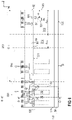
- FIG. 4 a top view of a semiconductor device comprising a sensor device 80 is exemplarily illustrated.
- the semiconductor body 100 may comprise a first longitudinal side L 1 , a second longitudinal side L 2 , a first narrow side B 1 , and a second narrow side B 2 .
- the first sensor region 83 may extend along each of the longitudinal sides L 1 , L 2 and along each of the narrow sides B 1 , B 2 at least partially.
- the second contact pad 82 is also schematically illustrated.
- the first contact pad 81 in this example similar to the example of FIG. 3A , is arranged vertically below the second contact pad 82 and is, therefore, concealed by the second contact pad 82 in this top view. This, however, is only an example. As has been described above, if one loop of the first sensor region 83 around the active region 220 is not fully completed, the horizontal positions of the first contact pad 81 and the second contact pad 82 may differ from each other.
- the first sensor region 83 may be arranged at a first distance d 1 from the respective outer edge 105 in a horizontal direction x, z.
- the horizontal direction x, z is perpendicular to the respective outer edge 105 .
- the horizontal field-stop-region 91 b has a first width d 91b in a first horizontal direction x.
- a ratio between the first distance d 1 and the first width d 91b is between 0.1 and 0.8.
- the horizontal field-stop-region 91 b may have a first width d 91b of between 10 ⁇ m and 150 ⁇ m.
- the first distance d 1 may be between 2 ⁇ m and 20 ⁇ m, for example.
- the first distance d 1 may be small enough to be able to detect cracks or chips, and may be great enough not to be influenced by surface charges or residues (e.g., AuSn residues) and not to be unintentionally damaged during separation of the individual semiconductor bodies 100 .
- a certain unevenness (fraying) of the outer edges 105 is common after separation of the semiconductor bodies 100 . It is generally unavoidable that the outer edges 105 are damaged (frayed) to a certain degree during separation. Such comparably small damages, however, do not affect the functionality of the semiconductor device.
- first sensor region 83 is arranged too close to the outer edges 105 , there is a risk that each individual semiconductor device is detected to be malfunctioning due to the typical fraying, even if no severe chips or cracks have formed in the semiconductor device. On the other hand, if the first sensor region 83 is arranged too far from the outer edge 105 , there is a risk that even severe chips or cracks may not be reliably detected.
- the first sensor region 83 may have a second width d 83 in the horizontal direction x, z.
- the second width d 83 may be between 2 ⁇ m and 10 ⁇ m, for example. However, according to another example, a second width d 83 of up to several 10 ⁇ m is also possible. However, the second width d 83 is less than the first width d 91b of the horizontal field-stop-region 91 b such that the first sensor region 83 may be completely enclosed by the horizontal field-stop-region 91 b in the horizontal directions x, z.
- the first sensor region 83 may be separated from the horizontal field-stop-region 91 b by means of a second sensor region 84 .
- the second sensor region 84 may surround the first sensor region 83 such that no direct connection is formed between the first sensor region 83 and the horizontal field-stop-region 91 b .
- the second sensor region 84 may be of the second doping type, for example.
- the second sensor region 84 may be arranged all around the first sensor region 83 except for those surfaces of the first sensor region 83 that are arranged adjacent to the first surface 101 and the semiconductor layer 110 , for example. This allows to electrically contact the first sensor region 83 .
- FIG. 6 schematically illustrates a cross sectional view of a semiconductor device in a section plane B-B′ (see FIG. 4 ). That is, the cross section of the first sensor region 83 in FIG. 6 is a cross section of one of the horizontal sections 831 extending along the second longitudinal side L 2 .
- FIG. 7 schematically illustrates a cross sectional view of a semiconductor device in a section plane C-C′ (see FIG. 4 ). That is, the cross section of the first sensor region 83 illustrated in FIG. 7 is a cross section of the first and second vertical sections 832 , 833 .
- the first vertical section 832 may be electrically coupled to a first contact pad on the second surface 102 (first contact pad 81 not specifically illustrated in FIG. 7 ).
- first contact pad 81 not specifically illustrated in FIG. 7
- an ohmic contact is formed only between the first sensor region 83 and the first contact pad 81 , but not between the second sensor region 84 and the first contact pad.
- the second vertical section 833 may be electrically coupled to the field plate electrode 44 by means of a contact plug.
- the contact plug may comprise at least one of tungsten, aluminum, copper, and a Ti/TiN barrier liner, for example.
- another contact plug electrically couples the field plate electrode 44 to the junction termination region 90 .
- the first contact pad 81 is formed by the drain node D (drain electrode or drain metallization) and the second contact pad 82 is formed by the source node S (source electrode 41 ).
- the drain metallization (not illustrated in the Figures), which is usually a continuous layer (non-structured layer) covering the drain region 36 , is not referred to as a “pad”.
- the drain metallization may be used as (form) the first contact pad 81 , the drain metallization in the following is designated as the “first contact pad” nevertheless.
- the electrical path between the drain node D and the source node S through the sensor device 80 is schematically illustrated in FIG. 8 .
- the first sensor region 83 and the second sensor region 84 are illustrated as vertical regions extending between the semiconductor layer 110 and the first surface 101 .
- Horizontal sections 831 are not specifically illustrated in FIG. 8 .
- the electrical path extends from the source electrode 41 through a first one of the contact plugs 42 to the base region 321 .
- the base region 321 acts as a first resistance R 1 .
- a first JFET T 1 may be formed by the base region 321 , the junction termination region 90 and the horizontal field-stop-region 91 b , wherein the junction termination region 90 and the horizontal field-stop-region 91 b may act as a gate of the first JFET T 1 .
- the base region 321 may extend from the first contact plug 42 (electrically coupling the source electrode 41 to the base region 321 ) to the second vertical section 833 and may adjoin the second sensor region 84 .
- the junction termination region 90 may not adjoin the second sensor region 84 .
- the electrical path further extends through another one of the contact plugs through the field plate electrode 44 and through a third one of the contact plugs 42 to the first sensor region 83 .
- the first sensor region 83 acts as a second resistance R 2 .
- the electrical path further extends from the first sensor region 83 through the semiconductor layer 110 to the drain electrode D.
- a sensor pad may be arranged above the second vertical section 833 of the sensor device 80 . That is, the field plate electrode 44 may be omitted in a section above the second vertical section 833 , but may be present in those sections along the outer edges 105 that are arranged above the horizontal sections 831 of the sensor device 80 .
- Such a dedicated sensor pad may be electrically coupled to the first sensor region 83 by means of a contact plug 42 .
- the first sensor region 83 acts as a resistor R 2 between the first contact pad 81 and the second contact pad 82 . If a chip or crack occurs, this affects the electrical properties of the first sensor region 83 , thereby altering the resistor value of the first sensor region 83 . That is, if a change of the resistor value of the first sensor region 83 is detected, this may be seen as an indicator that a chip or crack occurred. Severe chips or cracks may also completely interrupt an electrical connection between the first contact pad 81 and the second contact pad 82 .
- the second transistor device T 2 illustrated in the circuit diagram of FIG. 9 corresponds to the transistor device formed by the plurality of transistor cells 30 .
- the sensor device 80 is electrically coupled in parallel to the second transistor device T 2 between the source node S and the drain node D.
- the first resistor R 1 , the first transistor device (JFET) T 1 , and the second resistor R 2 are coupled in series between the source node S and the drain node D.
- a gate node of the first transistor device T 1 is coupled to the drain node D.
- the first transistor device T 1 may be a p-channel JFET, as the current carrying path between its source and its drain may be formed by the base region 321 , which may be a p-type region.
- the first transistor device T 1 is an n-channel JFET, if the base region 321 is an n-type region.
- the second transistor device TT 2 may represent a p-type resistor. This results in an applicable drain-source current of the sensor device 80 in the range of several 100 nA up to several 100 ⁇ A or even up to several 1 mA. When a chip or crack occurs, the resistance value of the second resistor R 2 significantly increases.
- FIG. 10 an exemplary circuit diagram of a circuit for detecting chip cracks is schematically illustrated.
- FIG. 10 schematically illustrates external circuitry that may be coupled to the first contact pad 81 and the second contact pad 82 .
- an external sense resistor R 3 may be coupled to the second contact pad 82 (sense pad SP).
- the sense resistor R 3 may be a high ohmic shunt resistor, for example.
- a measuring voltage V batt may be applied via a series connection of the second resistor R 2 and the sense resistor R 3 . If a chip or a crack occurs which extends into the first sensor region 83 , the resulting sensing current decreases.
- the sensing voltage V meas across the sense resistor R 3 will significantly decrease.
- the voltage drop of the sensing voltage V meas may be detected by a detection circuit comprising, e.g., an operational amplifier OA.
- the amplified voltage may be provided to a level shifter LS which may shift the amplified voltage to a lower electrical potential in order to be able to provide the voltage to a microcontroller ⁇ C.
- the microcontroller ⁇ C may be configured to evaluate the detected voltage, detect whether a chip or crack occurred, and to set the semiconductor device to a safe state and to generate a warning, for example, if a chip or crack has been detected.
- the circuit illustrated in FIG. 10 is only an example. Any other suitable circuit may be used to detect a chip or crack which corrupts the first sensor region 83 .
- the gate electrodes 33 of the transistor cells 30 may be provided as a plurality of longitudinal semiconductor regions.
- a length of the gate electrodes 33 in the second horizontal direction z may be considerably larger than a respective width in the first horizontal direction x, the horizontal directions x, z being perpendicular to each other.
- the gate electrodes 33 may have an elongated form that is similar to the form of the compensation regions 38 .
- Each of the gate electrodes 33 may be electrically connected to a gate runner 10 , for example.
- the gate runner 10 may be a circumferential, electrically conducting layer which electrically couples the gate electrodes 33 to the gate pad 43 .
- the gate runner 10 overlaps each of the longitudinal gate electrodes 33 , that is, at least one end of each of the gate electrodes 33 is located below the gate runner 10 in the vertical direction y.
- all ends of the gate electrodes 33 that are overlapped by the gate runner 10 are electrically connected to the gate runner 10 .
- it is also possible that some ends that are overlapped by the gate runner 10 are not directly connected to the gate runner 10 (not illustrated in the Figures). “Not directly connected” means that there is no contact plug between the longitudinal end of the respective gate electrodes 33 and the gate runner 10 .
- such longitudinal ends may still be indirectly connected to the gate runner 10 via another one of the gate electrodes 33 .
- an insulation layer 51 is formed on top of the first surface 101 of the semiconductor body 100 .
- the gate runner 10 may be formed on this insulation layer 51 .
- a source region 31 is illustrated in dashed lines in FIG. 11 , as it is arranged in a plane different from the plane that is illustrated in the Figure and is not immediately visible in the cross-section of FIG. 11 .
- the contact plugs 42 may be provided as a plurality of longitudinal regions. A length of the contact plugs 42 in the second horizontal direction z may be considerably larger than a respective width in the first horizontal direction x.
- the boundary between the edge region 210 and the active region 220 is usually defined by the lateral end of the source region 31 or, more specifically, by a contact plug 43 electrically coupling the base region 321 to the source electrode 41 . That is, the width d 210 of the edge region 210 generally corresponds to a distance between the contact plug 43 that electrically couples the base region 321 to the source electrode 41 and the outer edge 105 of the semiconductor body 100 . This, however, is only an example.
- FIG. 11 schematically illustrates a cross-section through one of the pillars formed by the drift region 35 .
- the doping concentration of the drift region 35 may decrease in the in the intrinsic region 91 a from the drift region towards the horizontal field-stop-region 91 b in the second horizontal direction z.
- the first semiconductor region 83 may extend in the edge region 210 along the narrow sides B 1 , B 2 in the same way as has been described with respect to the longitudinal sides L 1 , L 2 in FIG. 6 above.
- the first contact pad 81 and the second contact pad 82 are arranged adjacent to the first longitudinal side L 1 of the semiconductor body 100 . This, however, is only an example. It is generally also possible to arrange the first contact pad 81 and the second contact pad 82 adjacent to any one of the first and second longitudinal sides L 1 , L 2 and the first and second narrow sides B 1 , B 2 .
- the first contact pad 81 and the second contact pad 82 do not necessarily need to be arranged adjacent to the same side L 1 , L 2 , B 1 , B 2 .
- the monolithically integrated sensor device 80 that has been described with respect to the Figures above allows to efficiently test semiconductor devices with regard to chips and cracks in a very fast and cost-effective way.
- the sensor device 80 is not active during normal operation of the transistor device formed by the plurality of transistor cells 30 .
Landscapes
- Metal-Oxide And Bipolar Metal-Oxide Semiconductor Integrated Circuits (AREA)
Abstract
Description
Claims (15)
Applications Claiming Priority (3)
| Application Number | Priority Date | Filing Date | Title |
|---|---|---|---|
| EP19167047 | 2019-04-03 | ||
| EP19167047.0A EP3719848A1 (en) | 2019-04-03 | 2019-04-03 | Semiconductor device |
| EP19167047.0 | 2019-04-03 |
Publications (2)
| Publication Number | Publication Date |
|---|---|
| US20200321463A1 US20200321463A1 (en) | 2020-10-08 |
| US11424358B2 true US11424358B2 (en) | 2022-08-23 |
Family
ID=66092059
Family Applications (1)
| Application Number | Title | Priority Date | Filing Date |
|---|---|---|---|
| US16/838,189 Active 2040-06-06 US11424358B2 (en) | 2019-04-03 | 2020-04-02 | Semiconductor device with sensor for crack detection |
Country Status (2)
| Country | Link |
|---|---|
| US (1) | US11424358B2 (en) |
| EP (1) | EP3719848A1 (en) |
Families Citing this family (1)
| Publication number | Priority date | Publication date | Assignee | Title |
|---|---|---|---|---|
| CN116018667A (en) * | 2020-09-17 | 2023-04-25 | 罗姆股份有限公司 | Semiconductor device |
Citations (6)
| Publication number | Priority date | Publication date | Assignee | Title |
|---|---|---|---|---|
| JP3357804B2 (en) | 1996-11-06 | 2002-12-16 | 株式会社東芝 | Semiconductor device and manufacturing method thereof |
| US20100207206A1 (en) * | 2004-05-19 | 2010-08-19 | Infineon Technologies Ag | Transistor |
| US20140367772A1 (en) | 2013-06-12 | 2014-12-18 | Infineon Technologies Austria Ag | Semiconductor Device Including a Drift Zone and a Drift Control Zone |
| US20150333060A1 (en) * | 2014-05-14 | 2015-11-19 | Infineon Technologies Ag | Semiconductor Device |
| DE102015106707A1 (en) | 2015-04-30 | 2016-11-03 | Infineon Technologies Austria Ag | Semiconductor devices and methods of forming a semiconductor device |
| US20170250255A1 (en) | 2016-02-25 | 2017-08-31 | Infineon Technologies Austria Ag | Semiconductor Device with Needle-Shaped Field Plate Structures in a Transistor Cell Region and in an Inner Termination Region |
-
2019
- 2019-04-03 EP EP19167047.0A patent/EP3719848A1/en not_active Withdrawn
-
2020
- 2020-04-02 US US16/838,189 patent/US11424358B2/en active Active
Patent Citations (6)
| Publication number | Priority date | Publication date | Assignee | Title |
|---|---|---|---|---|
| JP3357804B2 (en) | 1996-11-06 | 2002-12-16 | 株式会社東芝 | Semiconductor device and manufacturing method thereof |
| US20100207206A1 (en) * | 2004-05-19 | 2010-08-19 | Infineon Technologies Ag | Transistor |
| US20140367772A1 (en) | 2013-06-12 | 2014-12-18 | Infineon Technologies Austria Ag | Semiconductor Device Including a Drift Zone and a Drift Control Zone |
| US20150333060A1 (en) * | 2014-05-14 | 2015-11-19 | Infineon Technologies Ag | Semiconductor Device |
| DE102015106707A1 (en) | 2015-04-30 | 2016-11-03 | Infineon Technologies Austria Ag | Semiconductor devices and methods of forming a semiconductor device |
| US20170250255A1 (en) | 2016-02-25 | 2017-08-31 | Infineon Technologies Austria Ag | Semiconductor Device with Needle-Shaped Field Plate Structures in a Transistor Cell Region and in an Inner Termination Region |
Also Published As
| Publication number | Publication date |
|---|---|
| EP3719848A1 (en) | 2020-10-07 |
| US20200321463A1 (en) | 2020-10-08 |
Similar Documents
| Publication | Publication Date | Title |
|---|---|---|
| US7906810B2 (en) | LDMOS device for ESD protection circuit | |
| JP5589052B2 (en) | Semiconductor device | |
| CN102714205B (en) | Bond pad with integrated transient overvoltage protection | |
| CN105428359B (en) | Semiconductor devices with current sensor | |
| US9728529B2 (en) | Semiconductor device with electrostatic discharge protection structure | |
| US9450019B2 (en) | Power semiconductor device, manufacturing method therefor, and method for operating the power semiconductor device | |
| US9735264B2 (en) | Semiconductor switch with integrated temperature sensor | |
| KR20080106951A (en) | ESD Protection Circuit and Method Having Separate Diode Devices | |
| US10971620B2 (en) | Method for producing a semiconductor arrangement | |
| KR101742447B1 (en) | Semiconductor device | |
| EP0242383A1 (en) | PROTECTING AN IGFET-INTEGRATED CIRCUIT FROM ELECTROSTATIC DISCHARGE. | |
| US20170271451A1 (en) | Semiconductor device | |
| KR102153550B1 (en) | Power semiconductor device | |
| US20110163384A1 (en) | Semiconductor device | |
| US11424358B2 (en) | Semiconductor device with sensor for crack detection | |
| US10290714B2 (en) | Transistor structure with field plate for reducing area thereof | |
| JP2025514117A (en) | Dynamic performance of on-chip current sensors | |
| CN112997294A (en) | Semiconductor device with a plurality of semiconductor chips | |
| US12021139B2 (en) | Semiconductor arrangement with an integrated temperature sensor | |
| US9196610B1 (en) | Semiconductor structure and electrostatic discharge protection circuit | |
| JP2014116507A (en) | Method of inspecting semiconductor device and semiconductor device | |
| US20230145562A1 (en) | Semiconductor device | |
| WO2005112134A2 (en) | High current mos device with avalanche protection and method of operation | |
| US12237412B2 (en) | Protection structures for semiconductor devices with sensor arrangements | |
| CN111415930A (en) | Electrostatic discharge protection structure and electrostatic discharge protection circuit |
Legal Events
| Date | Code | Title | Description |
|---|---|---|---|
| FEPP | Fee payment procedure |
Free format text: ENTITY STATUS SET TO UNDISCOUNTED (ORIGINAL EVENT CODE: BIG.); ENTITY STATUS OF PATENT OWNER: LARGE ENTITY |
|
| AS | Assignment |
Owner name: INFINEON TECHNOLOGIES DRESDEN GMBH & CO. KG, GERMANY Free format text: ASSIGNMENT OF ASSIGNORS INTEREST;ASSIGNORS:WEYERS, JOACHIM;BOEHM, ANDREAS;HIRLER, FRANZ;AND OTHERS;REEL/FRAME:052378/0452 Effective date: 20200403 |
|
| STPP | Information on status: patent application and granting procedure in general |
Free format text: DOCKETED NEW CASE - READY FOR EXAMINATION |
|
| STPP | Information on status: patent application and granting procedure in general |
Free format text: NON FINAL ACTION MAILED |
|
| STPP | Information on status: patent application and granting procedure in general |
Free format text: RESPONSE TO NON-FINAL OFFICE ACTION ENTERED AND FORWARDED TO EXAMINER |
|
| STPP | Information on status: patent application and granting procedure in general |
Free format text: NOTICE OF ALLOWANCE MAILED -- APPLICATION RECEIVED IN OFFICE OF PUBLICATIONS |
|
| STPP | Information on status: patent application and granting procedure in general |
Free format text: PUBLICATIONS -- ISSUE FEE PAYMENT VERIFIED |
|
| STCF | Information on status: patent grant |
Free format text: PATENTED CASE |