US11424237B2 - Memory device - Google Patents
Memory device Download PDFInfo
- Publication number
- US11424237B2 US11424237B2 US16/928,988 US202016928988A US11424237B2 US 11424237 B2 US11424237 B2 US 11424237B2 US 202016928988 A US202016928988 A US 202016928988A US 11424237 B2 US11424237 B2 US 11424237B2
- Authority
- US
- United States
- Prior art keywords
- lines
- program
- program lines
- decoders
- twisted
- Prior art date
- Legal status (The legal status is an assumption and is not a legal conclusion. Google has not performed a legal analysis and makes no representation as to the accuracy of the status listed.)
- Active, expires
Links
Images


Classifications
-
- H—ELECTRICITY
- H10—SEMICONDUCTOR DEVICES; ELECTRIC SOLID-STATE DEVICES NOT OTHERWISE PROVIDED FOR
- H10D—INORGANIC ELECTRIC SEMICONDUCTOR DEVICES
- H10D89/00—Aspects of integrated devices not covered by groups H10D84/00 - H10D88/00
- H10D89/10—Integrated device layouts
-
- H01L27/0207—
-
- G—PHYSICS
- G11—INFORMATION STORAGE
- G11C—STATIC STORES
- G11C11/00—Digital stores characterised by the use of particular electric or magnetic storage elements; Storage elements therefor
- G11C11/21—Digital stores characterised by the use of particular electric or magnetic storage elements; Storage elements therefor using electric elements
- G11C11/34—Digital stores characterised by the use of particular electric or magnetic storage elements; Storage elements therefor using electric elements using semiconductor devices
- G11C11/40—Digital stores characterised by the use of particular electric or magnetic storage elements; Storage elements therefor using electric elements using semiconductor devices using transistors
- G11C11/41—Digital stores characterised by the use of particular electric or magnetic storage elements; Storage elements therefor using electric elements using semiconductor devices using transistors forming static cells with positive feedback, i.e. cells not needing refreshing or charge regeneration, e.g. bistable multivibrator or Schmitt trigger
- G11C11/413—Auxiliary circuits, e.g. for addressing, decoding, driving, writing, sensing, timing or power reduction
-
- G—PHYSICS
- G06—COMPUTING OR CALCULATING; COUNTING
- G06F—ELECTRIC DIGITAL DATA PROCESSING
- G06F30/00—Computer-aided design [CAD]
- G06F30/30—Circuit design
- G06F30/39—Circuit design at the physical level
- G06F30/392—Floor-planning or layout, e.g. partitioning or placement
-
- G—PHYSICS
- G06—COMPUTING OR CALCULATING; COUNTING
- G06F—ELECTRIC DIGITAL DATA PROCESSING
- G06F30/00—Computer-aided design [CAD]
- G06F30/30—Circuit design
- G06F30/39—Circuit design at the physical level
- G06F30/394—Routing
-
- G—PHYSICS
- G11—INFORMATION STORAGE
- G11C—STATIC STORES
- G11C11/00—Digital stores characterised by the use of particular electric or magnetic storage elements; Storage elements therefor
- G11C11/21—Digital stores characterised by the use of particular electric or magnetic storage elements; Storage elements therefor using electric elements
- G11C11/34—Digital stores characterised by the use of particular electric or magnetic storage elements; Storage elements therefor using electric elements using semiconductor devices
- G11C11/40—Digital stores characterised by the use of particular electric or magnetic storage elements; Storage elements therefor using electric elements using semiconductor devices using transistors
- G11C11/41—Digital stores characterised by the use of particular electric or magnetic storage elements; Storage elements therefor using electric elements using semiconductor devices using transistors forming static cells with positive feedback, i.e. cells not needing refreshing or charge regeneration, e.g. bistable multivibrator or Schmitt trigger
- G11C11/413—Auxiliary circuits, e.g. for addressing, decoding, driving, writing, sensing, timing or power reduction
- G11C11/417—Auxiliary circuits, e.g. for addressing, decoding, driving, writing, sensing, timing or power reduction for memory cells of the field-effect type
- G11C11/418—Address circuits
-
- G—PHYSICS
- G11—INFORMATION STORAGE
- G11C—STATIC STORES
- G11C5/00—Details of stores covered by group G11C11/00
- G11C5/02—Disposition of storage elements, e.g. in the form of a matrix array
- G11C5/025—Geometric lay-out considerations of storage- and peripheral-blocks in a semiconductor storage device
-
- G—PHYSICS
- G11—INFORMATION STORAGE
- G11C—STATIC STORES
- G11C7/00—Arrangements for writing information into, or reading information out from, a digital store
- G11C7/10—Input/output [I/O] data interface arrangements, e.g. I/O data control circuits, I/O data buffers
- G11C7/1006—Data managing, e.g. manipulating data before writing or reading out, data bus switches or control circuits therefor
- G11C7/1009—Data masking during input/output
-
- G—PHYSICS
- G11—INFORMATION STORAGE
- G11C—STATIC STORES
- G11C8/00—Arrangements for selecting an address in a digital store
- G11C8/14—Word line organisation; Word line lay-out
-
- H01L27/1104—
-
- H01L27/1116—
-
- H—ELECTRICITY
- H10—SEMICONDUCTOR DEVICES; ELECTRIC SOLID-STATE DEVICES NOT OTHERWISE PROVIDED FOR
- H10B—ELECTRONIC MEMORY DEVICES
- H10B10/00—Static random access memory [SRAM] devices
- H10B10/12—Static random access memory [SRAM] devices comprising a MOSFET load element
-
- H—ELECTRICITY
- H10—SEMICONDUCTOR DEVICES; ELECTRIC SOLID-STATE DEVICES NOT OTHERWISE PROVIDED FOR
- H10B—ELECTRONIC MEMORY DEVICES
- H10B10/00—Static random access memory [SRAM] devices
- H10B10/18—Peripheral circuit regions
-
- G—PHYSICS
- G11—INFORMATION STORAGE
- G11C—STATIC STORES
- G11C8/00—Arrangements for selecting an address in a digital store
- G11C8/10—Decoders
Definitions
- Static random access memory is one type of semiconductor memory having an array of memory cells.
- a specified memory cell is activated by a corresponding word line and a corresponding bit line, and both of the word lines and the bit lines are selected by a control circuit comprising address lines.
- the SRAM is designed according to routing, for example, including the word lines, the bit lines and the address lines, and parasitic capacitance thereof.
- FIG. 1 is a schematic diagram of a memory device, in accordance with some embodiments of the present disclosure.
- FIG. 2 is a schematic diagram of a memory device shown in FIG. 1 , in accordance with some embodiments of the present disclosure.
- FIG. 3 is a flow chart of a method for generating a layout design of a memory device shown in FIG. 2 , in accordance with some embodiments of the present disclosure.
- FIGS. 4A-4B are schematic diagrams of a memory device, to be operated in a method in FIG. 3 , in accordance with some embodiments of the present disclosure.
- FIG. 5 is a layout diagram of a memory device shown in FIG. 2 , in accordance with some embodiments of the present disclosure.
- FIG. 6 is a schematic diagram of a memory device shown in FIG. 1 , in accordance with some embodiments of the present disclosure.
- FIG. 7 is a schematic diagram of a memory device shown in FIG. 1 , in accordance with some embodiments of the present disclosure.
- FIG. 8 is a schematic diagram of a memory device shown in FIG. 1 , in accordance with some embodiments of the present disclosure.
- FIG. 9 is a schematic diagram of a memory device shown in FIG. 1 , in accordance with some embodiments of the present disclosure.
- FIG. 10 is a block diagram of a system for designing an IC layout design, in accordance with some embodiments of the present disclosure.
- FIG. 11 is a block diagram of an IC manufacturing system, and an IC manufacturing flow associated therewith, in accordance with some embodiments of the present disclosure.
- first and second features are formed in direct contact
- additional features may be formed between the first and second features, such that the first and second features may not be in direct contact
- present disclosure may repeat reference numerals and/or letters in the various examples. This repetition is for the purpose of simplicity and clarity and does not in itself dictate a relationship between the various embodiments and/or configurations discussed.
- first may be termed a second element, and, similarly, a second element could be termed a first element, without departing from the scope of the embodiments.
- the term “and/or” includes any and all combinations of one or more of the associated listed items.
- Coupled may also be termed as “electrically coupled”, and the term “connected” may be termed as “electrically connected”. “Coupled” and “connected” may also be used to indicate that two or more elements cooperate or interact with each other.
- spatially relative terms such as “underlying,” “below,” “lower,” “overlying,” “upper” and the like, may be used throughout the description for ease of understanding to describe one element or feature's relationship to another element(s) or feature(s) as illustrated in the figures.
- the spatially relative terms are intended to encompass different orientations of the device in use or operation in addition to the orientation depicted in the figures.
- the structure may be otherwise oriented (e.g., rotated 90 degrees or at other orientations) and the spatially relative descriptors used herein may likewise be interpreted accordingly.
- “around”, “about”, “approximately” or “substantially” shall generally refer to any approximate value of a given value or range, in which it is varied depending on various arts in which it pertains, and the scope of which should be accorded with the broadest interpretation understood by the person skilled in the art to which it pertains, so as to encompass all such modifications and similar structures. In some embodiments, it shall generally mean within 20 percent, preferably within 10 percent, and more preferably within 5 percent of a given value or range. Numerical quantities given herein are approximate, meaning that the term “around”, “about”, “approximately” or “substantially” can be inferred if not expressly stated, or meaning other approximate values.
- FIG. 1 illustrates a schematic diagram of a memory device 100 , in accordance with some embodiments of the present disclosure.
- the memory device 100 is implemented by static random access memory (SRAM).
- SRAM static random access memory
- the memory device 100 includes an array of memory cells 110 a , an array of memory cells 110 b , a program circuit 120 , a control circuit 130 , an input/output (I/O) circuitry 140 a and an I/O circuitry 140 b .
- the program circuit 120 is disposed between the array of memory cells 110 a and the array of memory cells 110 b , and is coupled through word lines (not shown in FIG. 1 ) to the array of memory cells 110 a and the array of memory cells 110 b .
- the control circuit 130 is coupled through address lines AL to the program circuit 120 , and is also indicated as “CTRL” in FIG. 1 .
- the control circuit 130 is further coupled to the I/O circuitry 140 a and the I/O circuitry 140 b .
- the I/O circuitry 140 a and the I/O circuitry 140 b are coupled to the array of memory cells 110 a and the array of memory cells 110 b , respectively.
- Each of the array of memory cells 110 a and the array of memory cells 110 b includes memory cells (not shown) arranged in rows and columns.
- each of the memory cells is configured to store a bit data based on signals transmitted from the I/O circuitry 140 a , the I/O circuitry 140 b and the word lines.
- each of the memory cells is implemented by 6 or 8 transistors.
- the program circuit 120 is also referred to a decoder circuit.
- the program circuit 120 includes word line decoders 121 arranged in columns, and each of the word line decoders 121 corresponds to one memory cell of the array of memory cells 110 a and one memory cells of the array of memory cells 110 b .
- each of the word line decoders 121 includes logic operators (not shown) to decode voltages of the address lines AL, for identifying which word line to be charged or be activated.
- the address lines AL are charged to logic high or logic low by a pre-decoder 131 included in the control circuit 130 , for selecting which memory cell to be read or be written in bit data.
- Each of the I/O circuitry 140 a and the I/O circuitry 140 b includes I/O circuits 141 arranged in rows, and each of the I/O circuits 141 corresponds to one memory cell of the array of memory cells 110 a or one memory cell of the array of memory cells 110 b , for reading or writing the bit data into the corresponding memory cell.
- the I/O circuits 141 are indicated as “I/O” in FIG. 1 .
- the number of the word line decoders 121 and the address lines AL is determined based on a total number of word lines in the array of memory cells 110 a and the array of memory cells 110 b .
- k address lines AL are used for 2 k word lines.
- one of the address lines AL is used when one of the array of memory cells 110 a or the array of memory cells 110 b includes two word lines
- two address lines AL are used when the array of memory cells 110 a or the array of memory cells 110 b includes three or four word lines
- three address lines AL are used when the array of memory cells 110 a or the array of memory cells 110 b includes four to eight word lines, and so on.
- the configuration of the memory device 100 as illustrated above is also given for illustrative purposes.
- Various configurations of the memory device 100 are within the contemplated scope of the present disclosure.
- the array of memory cells 110 a and the array of memory cells 110 b are disposed abutting to each other, and are also referred to as one array of memory cells.
- the array of memory cells 110 a and the array of memory cells 110 b are identical to each other.
- the word line decoders 121 and the address lines AL labeled as “AM” in FIG. 1 , is further discussed below.
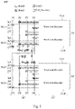
- FIG. 2 is a schematic diagram of a memory device AM corresponding to a part of the memory device 100 shown in FIG. 1 , in accordance with some embodiments of the present disclosure.
- like elements in FIG. 2 are designated with the same reference numbers for ease of understanding.
- memory cells of the array of memory cells 110 a , the control circuit 130 and the I/O circuitry 140 a are not shown in FIG. 2 .
- the memory device AM includes word line decoders 121 grouped into groups G 1 and G 2 , sets of word lines WL 1 -WL 4 , and twisted address lines AL which are twisted at a twisted spot N.
- the word line decoders 121 include the word line decoder 121 a , 121 b , 121 c and 121 d arranged in columns.
- each of the word line decoders 121 a , 121 b , 121 c and 121 d is referenced as 121 hereinafter for illustration, because each of the word line decoder 121 a , 121 b , 121 c and 121 d operates in a similar way in some embodiments.
- Each of the word line decoders 121 is coupled to the corresponding set of word lines WL 1 , WL 2 , WL 3 and WL 4 , respectively, for receiving signals transmitted from the address lines AL.
- the word line decoder 121 a is coupled to a set of word lines WL 1 including the word lines A 1 , B 1 , C 1 and D 1
- the word line decoder 121 b is coupled to a set of word lines WL 2 including the word lines A 2 , B 2 , C 2 and D 2
- the word line decoder 121 c is coupled to a set of word lines WL 3 including the word lines A 3 , B 3 , C 3 and D 3
- the word line decoder 121 d is coupled to a set of word lines WL 4 including the word lines A 4 , B 4 , C 4 and D 4 .
- each of the word line A 1 -A 4 , B 1 -B 4 , C 1 -C 4 and D 1 -D 4 is referenced as WL hereinafter for illustration, because each of the word lines A 1 -A 4 , B 1 -B 4 , C 1 -C 4 and D 1 -D 4 operates in a similar way in some embodiments.
- Each of the word lines WL extends from a via (which is illustrated as a spot at the intersection with both of the word lines WL and the address lines AL) to the corresponding word line decoders 121 .
- the word line A 1 extends from the via (which is a spot interacted with the word line A 1 and the address line [ 3 ]) to the word line decoder 121 a .
- the word line A 1 is a metal line extending from the via to the word line decoder 121 a .
- a length of the word line A 1 is a length from the via to the word line decoder 121 a.
- the word line decoders 121 a , the word line decoders 121 b and other word line decoders (not shown) disposed between the word line decoders 121 a and the word line decoders 121 b are indicated as a group G 1 .
- the word line decoders 121 c , the word line decoders 121 d and other word line decoders (not shown) disposed between the word line decoders 121 c and the word line decoders 121 d are indicated as another group G 2 that is disposed next to the group G 1 .
- the word line decoders 121 are split into groups including a first group G 1 and a second group G 2 that is disposed next to the first group G 1 . Therefore, the word lines coupled to the corresponding word line decoders 121 are also split into the groups correspondingly.
- the number and arrangement of the word line decoders 121 or the word lines WL shown in FIG. 2 are given for illustrative purposes. Various numbers and arrangements of the word line decoders 121 or the word lines WL to implement the memory device AM in FIG. 2 are within the contemplated scope of the present disclosure.
- the memory device AM in addition to the word line decoders 121 a , 121 b , 121 c and 121 d shown in FIG. 2 , the memory device AM includes more than one word line decoder coupled to another set of the word lines.
- the word line decoder 121 a in addition to the word lines A 1 , B 1 , C 1 and D 1 included in the first set of word lines shown in FIG. 2 , the word line decoder 121 a includes more than one word line.
- the address lines AL extend substantially along columns.
- the address lines AL include address lines [ 1 ], [ 2 ], [ 3 ] and [ 4 ], and the address lines AL are intersected with the word lines WL that are extending along rows, for transmitting signals output from a pre-decoder (e.g., the pre-decoder 131 shown in FIG. 1 ) to the corresponding word line decoders 121 .
- a pre-decoder e.g., the pre-decoder 131 shown in FIG. 1
- Each of the address lines [ 1 ], [ 2 ], [ 3 ] and [ 4 ] is coupled through the via to each of the word line decoders 121 correspondingly.
- the address line [ 1 ] is coupled through the word line C 1 to the word line decoder 121 a , coupled through the word line B 2 to the word line decoder 121 b , coupled through the word line A 3 to the word line decoder 121 c , and coupled through the word line D 4 to the word line decoder 121 d .
- the address line [ 2 ] is coupled through the word line D 1 to the word line decoder 121 a , coupled through the word line A 2 to the word line decoder 121 b , coupled through the word line B 3 to the word line decoder 121 c , and coupled through the word line C 4 to the word line decoder 121 d .
- the address line [ 3 ] is coupled through the word line A 1 to the word line decoder 121 a , coupled through the word line D 2 to the word line decoder 121 b , coupled through the word line C 3 to the word line decoder 121 c , and coupled through the word line B 2 to the word line decoder 121 d .
- the address line [ 4 ] is coupled through the word line B 1 to the word line decoder 121 a , coupled through the word line C 2 to the word line decoder 121 b , coupled through the word line D 3 to the word line decoder 121 c , and coupled through the word line A 4 to the word line decoder 121 d.
- the address lines AL are twisted between the word lines of the group G 1 and the word lines of the group G 2 , and it is label as a spot N in FIG. 2 .
- the address lines AL are twisted and have a twisted spot N.
- the twisted spot N is disposed between the word lines WL of the abutting groups G 1 and G 2 .
- each of the address lines [ 1 ], [ 2 ], [ 3 ] and [ 4 ] are twisted and have a twisted spot N.
- the twisted spot N is disposed between the word lines A 2 -D 2 of the group G 1 and the word lines A 3 -D 3 of the group G 2 .
- the two adjacent word lines WL have different lengths.
- the word lines WL have lengths different from each other.
- a length of the word line A 1 is different from any of a length of the word line B 1 , a length of the word line C 1 , or a length of the word line D 1 .
- At least one of the word lines WL of one group (e.g., group G 1 ) and at least one of the word lines WL of another group (e.g., group G 2 ) have same lengths.
- one of the word lines WL has a length that is as same as a length of one of the word lines WL of another group (e.g., group G 2 ).
- a length of the word line A 1 of the group G 1 is equal to a length of the word line B 3 of the group G 2 .
- the word lines WL of the different groups have same total lengths.
- a total length of the word lines WL of one group is equal to a total length of the word lines WL of another group (e.g., group G 2 ).
- a total length of the word lines, including the word lines A 1 -D 1 and A 2 -D 2 of the group G 1 is equal to a total length of the word lines, including the word lines A 3 -D 3 and A 4 -D 4 of the group G 2 .
- the word lines WL that are interacted with the different address lines AL have same total lengths.
- a total length of the word lines WL that are interacted with the corresponding address lines AL is as same as one another. That is, a total length of the word lines WL that are coupled to one of the address lines AL is equal to a total length of the word lines WL that are coupled to another one of the address lines AL.
- a total length of the word lines WL includes a length of word line C 1 , a length of word line B 2 , a length of word line A 3 and a length of word line D 4 .
- a total length of the word lines WL indicated as a second length, includes a length of word line D 1 , a length of word line A 2 , a length of word line B 3 and a length of word line C 4 .
- a total length of the word lines WL includes a length of word line A 1 , a length of word line D 2 , a length of word line C 3 and a length of word line B 4 .
- a total length of the word lines WL includes a length of word line B 1 , a length of word line C 2 , a length of word line D 3 and a length of word line A 4 .
- the first length, the second length, the third length, and the fourth length are as same as each other.
- the above configuration of the memory device AM is provided for illustrative purposes.
- Various implementations of the memory device AM are within the contemplated scope of the present disclosure.
- the twisted lines are implemented by other signal lines, including, for example, output metal lines coupled to the pre-decoder (which is shown in FIG. 1 ), input metal lines coupled to the pre-decoder, input vias coupled to the word line decoders 121 , output metal lines coupled to the word line decoders 121 , or all combinations thereof.
- the twisted lines are implemented in other metal layers, including, for example, other metal layers rather than M1 or M2 layer, layers disposed with vias, layers disposed with poly segments for forming gates of transistors, layers disposed with active area for forming transistors, any conductors, or all combinations thereof.
- some of the word lines that are interacted with the corresponding address lines have total lengths that are different from one another by cutting the redundant routings of the word lines. Since a length of the word lines corresponds to a parasitic capacitance. As the length being longer, the parasitic capacitance being higher. If a total length of the word lines corresponds to each of the address lines is different from one another, the parasitic capacitance corresponds to each of the address lines is also different from one another, and it is also indicated as unbalanced parasitic capacitance. The unbalanced parasitic capacitance would lead to poor performance of the memory device.
- the memory device AM keeps the balanced parasitic capacitance with redundant routings of the word lines. Furthermore, a total parasitic capacitance of the memory device AM is reduced compared to the above approaches. On the other hand, in the embodiments of the present disclosure, it does not affect circuit operations of the memory device AM, area design of the memory device AM and design rule of a layout for implementing the memory device AM.
- FIG. 3 is a flow chart of a method 300 for generating a layout design of a memory device AM shown in FIG. 2 , in accordance with some embodiments of the present disclosure.
- Following illustrations of the method 300 in FIG. 3 with reference to the memory device AM in FIG. 2 include exemplary operations. However, the operations in FIG. 3 are not necessarily performed in the order shown. Alternatively stated, operations may be added, replaced, changed order, and/or eliminated as appropriate, in accordance with the spirit and scope of various embodiments of the present disclosure.
- the word lines and the address lines are arranged in the memory device.
- the word lines WL and the address lines AL are arranged in the memory device AM.
- the word lines are arranged in rows
- the address lines are arranged in columns
- the word lines and the address lines are interacted to each other.
- the vias are further arranged at the interaction with both of the word lines and the address lines, for coupling the word lines and the address lines to each other.
- the vias are arranged at the interaction with both of the word lines WL and the address lines AL.
- first word lines and second word lines are grouped from the word lines.
- the word lines are grouped or split into two groups corresponding to the first word lines and the second word lines.
- the word lines WL are grouped into the groups G 1 and G 2 , wherein the group G 1 includes the word lines A 1 -D 1 and A 2 -D 2 , and the group G 2 includes the word lines A 3 -D 3 and A 4 -D 4 .
- the word lines are split into several groups, including, for example, one group including first word lines and another group including second word lines.
- the word lines are split into three groups (which is discussed with reference to FIG. 7 ).
- the word lines are split into four groups (which is discussed with reference to FIG. 8 ).
- Various configurations of grouping word lines are within the contemplated scope of the present disclosure.
- FIG. 4A is a schematic diagrams of a memory device AM, to be performed in operations including S 310 and S 320 in the method 300 in FIG. 3 , in order to form the memory device AM shown in FIG. 2 , in accordance with some embodiments of the present disclosure.
- FIG. 4A like elements in FIG. 4A are designated with the same reference numbers for ease of understanding.
- sets of word lines WL 1 -WL 4 including corresponding word lines A 1 -D 1 , A 2 -D 2 , A 3 -D 3 and A 4 -D 4 (which are also referenced as WL for simplicity), are arranged in rows and are coupled to the corresponding word line decoders 121 a - 121 d .
- the address lines AL including the address lines [ 1 ]-[ 4 ], are arranged in columns and are interacted with the word lines WL.
- the vias are arranged at the interaction with both of the word lines WL and the address lines AL, based on the circuit design of the memory device AM. Accordingly, the address lines AL are coupled through the vias to the word lines WL, and the word lines WL are coupled to the word line decoders 121 .
- the word lines WL are grouped into the group G 1 and the group G 2 .
- the corresponding word line decoders 121 are grouped into the group G 1 and the group G 2 .
- the word line decoders 121 a , 121 b and the corresponding word lines A 1 -D 1 , A 2 -D 2 are grouped as the group G 1 .
- the word line decoders 121 c , 121 d and the corresponding word lines A 3 -D 3 , A 4 -D 4 are grouped as the group G 2 .
- the group G 1 is disposed next to the group G 2 .
- the group G 1 and the group G 2 are abutting to each other.
- the address lines are twisted at at least one twisted spot.
- the address lines AL are twisted at at least one twisted spot including, for example, the twisted spot N.
- the address lines are twisted with respect to rows and are flipped from the right to the left.
- the address lines are twisted more than once, and have more than one twisted spot.
- the address lines have two twisted spots; and with reference to FIG. 8 , the address lines have three twisted spots.
- plenty of the twisted spots are aligned with one column that is at a center column between the address lines.
- a number of the twisted times of address lines is based on a number of word line decoders coupled to the first word lines (indicated as a first number for simplicity) and a number of word line decoders coupled to the second word lines (indicated as a second number for simplicity).
- the address lines are twisted in a twisted number.
- the twisted number is determined according to numbers of word line decoders of corresponding groups that is grouped in operation S 320 . For example, in some other embodiments, when the first number is an even number, and the second number is an even number as well, the twisted number is more than one. In various embodiments, when one of the first number and the second number is an odd number, the twisted number is an odd number as well.
- the vias on the twisted address lines are mirrored from the vias on the untwisted address lines.
- the vias are mirrored from the original vias disposed over both of the address lines and one of the word lines, with respect to a column disposed across the twisted spot.
- the vias are flipped/twisted with the address lines together. Therefore, the word lines and the address lines have a same connection as that is operated before the operation S 330 .
- the vias are disposed over the twisted address lines AL and the word lines WL, by mirroring the vias from the vias on both of the untwisted address lines (not shown in FIG. 2 ) and the word lines WL of the group G 1 to form the vias on the same.
- FIG. 4B is a schematic diagrams of a memory device AM, to be performed in operations including S 330 and S 340 in the method 300 in FIG. 3 , in order to from the memory device AM shown in FIG. 2 , in accordance with some embodiments of the present disclosure.
- FIG. 4B With respect to the embodiments of FIG. 2 or FIG. 4A , like elements in FIG. 4B are designated with the same reference numbers for ease of understanding.
- the address lines AL are twisted at the twisted spot N, and the twisted spot N is disposed between the group G 1 and the group G 2 , or also between the first word lines of the group G 1 and the second word lines of the group G 2 , in another way of explanation.
- the vias of the group G 1 are disposed over the twisted address lines AL (i.e., the address lines AL in FIG. 4B ) by mirroring vias of the group G 1 disposed over the untwisted address lines (i.e., the address lines AL in FIG. 4A ) and the corresponding word lines WL (e.g., the set of word lines WL 1 ), with respect to a column (not shown in FIG. 4B ) disposed across the twisted spot N, to form vias of the group G 1 shown in FIG. 4B .
- the number and arrangement of the twisted spot N are given for illustrative purposes. Various numbers and arrangements of the twisted spot N are within the contemplated scope of the present disclosure.
- the twisted spot N is disposed between the word lines of one group. In some other embodiments, a number of the twisted spot N is more than one and the twisted spots are disposed between word lines of different groups.
- operation S 350 part of the first word lines and the second word lines are cut off, to form the word lines included in the memory device.
- the redundant routings of both of the first word lines and the second word lines are removed, since the first word lines or the second word lines are coupled from the vias to the corresponding word line decoders.
- the word lines WL included in the memory device AM are generated by cutting off part of the word lines WL of the group G 1 and the word lines WL of the group G 2 .
- a layout design of the memory device is generated.
- the memory device includes the twisted address lines, the word lines and the word line decoders discussed above.
- the layout design of the memory device AM including the twisted address lines AL, the word lines WL and the word line decoders 121 , is generated.
- the address lines AL are twisted at the twisted spot N, and each of the word lines WL that are coupled to the corresponding word line decoders 121 has a length which is different from each other. Furthermore, a total length of the word lines WL that are coupled to one of the address lines AL is equal to a total length of the word lines WL that are coupled to another one of the address lines AL.
- FIG. 5 is a layout diagram AM′ of a memory device AM shown in FIG. 2 , and is also after operations including S 310 , S 320 , S 330 , S 340 and S 350 , in accordance with some embodiments of the present disclosure.
- the layout diagram AM′ includes word line decoders 121 ′, sets of word lines WL 1 ′, WL 2 ′, WL 3 ′ and WL 4 ′ (which are referenced as WL′ for simplicity), address lines AL′ and vias (not labeled, which is illustrated as a square with a cross inside).
- the layout diagram AM′ corresponds to the memory device AM shown in FIG. 2 ;
- the word line decoders 121 ′ correspond to the word line decoders 121 shown in FIG. 2 ;
- the word lines WL′ correspond to the word lines WL shown in FIG. 2 ;
- the address lines AL′ correspond to the address lines AL shown in FIG. 2 ;
- the vias correspond to the vias shown in FIG. 2 .
- the memory device AM is implemented with the same layout as the layout diagram AM′.
- the word line decoders 121 ′ are formed in a cell boundary (indicated as “Cell Boundary” in FIG. 5 ) that is disposed in a second metal (M2, also indicated as “Metal2” in FIG. 5 ) layer, and the word line decoders 121 ′ includes a word line decoder 121 a ′, a word line decoder 121 b ′, a word line decoder 121 c ′ and a word line decoder 121 d ′ that are arranged in columns.
- the sets of word lines WL 1 ′, WL 2 ′, WL 3 ′ and WL 4 ′ are formed in the M2 layer and are coupled to the word line decoders 121 ′ correspondingly.
- the set of word lines WL 1 ′ includes word lines A 1 ′-D 1 ′ and is coupled to the word line decoders 121 a ′;
- the set of word lines WL 2 ′ includes word lines A 2 ′-D 2 ′ and is coupled to the word line decoders 121 b ′;
- the set of word lines WL 3 ′ includes word lines A 3 ′-D 3 ′ and is coupled to the word line decoders 121 c ′;
- the set of word lines WL 4 ′ includes word lines A 4 ′-D 4 ′ and is coupled to the word line decoders 121 d′.
- the address lines AL′ are twisted and formed in at least one metal layers.
- the at least one metal layer includes the M2 layer and a third metal (M3, also indicated as “Metal3” in FIG. 5 ) layer that is disposed above the M2 layer.
- the address lines AL′ are interacted with the word lines WL′.
- the address lines AL′ include an address line [ 1 ]′ that is coupled through the vias to the word line C 1 , the word line B 2 , the word line A 3 , and the word line D 4 , respectively, wherein the vias are formed between the M2 layer and the M3 layer (also indicated as “VIA23” in FIG. 5 ), for coupling metal segments in M2 layer to metal segments in M3 layer.
- the address lines AL′ include an address line [ 2 ]′ that is coupled through the vias to the word line D 1 , the word line A 2 , the word line B 3 , and the word line C 4 , respectively; an address line [ 3 ]′ that is coupled through the vias to the word line A 1 , the word line D 2 , the word line C 3 , and the word line B 4 , respectively; and an address line [ 4 ]′ that is coupled through the vias to the word line B 1 , the word line C 2 , the word line D 3 , and the word line A 4 , respectively.
- one of the twisted address lines AL′ is implemented by a twisted metal trace formed in the M2 layer.
- the address line [ 1 ]′ is twisted and disposed in the M2 layer.
- one of the twisted address lines AL′ is implemented by several metal segments including at least one straight metal trace formed in the M2 layer and at least one twisted metal trace formed in the M3 layer. The twisted metal trace formed in the M3 layer is coupled through vias to the straight metal trace formed in the M2 layer, and the twisted metal trace is generated to form one of the twisted the address line AL′.
- FIG. 5 the address line [ 1 ]′ is twisted and disposed in the M2 layer.
- one of the twisted address lines AL′ is implemented by several metal segments including at least one straight metal trace formed in the M2 layer and at least one twisted metal trace formed in the M3 layer. The twisted metal trace formed in the M3 layer is coupled through vias to the straight metal trace formed in the M2 layer, and the twisted metal trace is generated to form one of the twisted
- the address line [ 2 ]′ is twisted and includes a straight metal trace corresponds to a group G 1 formed in the M2 layer, a twisted metal trace formed in the M3 layer, and an another straight metal trace corresponds to a group G 2 formed in the M2 layer.
- the M3 layer refers to any one of metal layers that is disposed above or below the M2 layer.
- FIG. 6 is a schematic diagram of a memory device AM corresponding to a part of the memory device 100 shown in FIG. 1 , and is also another memory device AM corresponding to the memory device AM shown in FIG. 2 , in accordance with some embodiments of the present disclosure.
- FIG. 6 like elements in FIG. 6 are designated with the same reference numbers for ease of understanding.
- the set of word lines WL 1 is split/grouped from other sets of word lines WL 2 -WL 4 and is indicated as the group G 1 .
- the remaining sets of word lines WL 2 -WL 4 including the word lines A 2 -D 2 , A 3 -D 3 , A 4 -D 4 coupled to the word line decoders 121 b , 121 c , 121 d correspondingly and other word lines (not shown) disposed between the word lines A 2 -D 2 and A 3 -D 3 , are indicated as the group G 2 . Similar to the embodiment illustrated in FIG.
- the address lines AL are twisted between the word lines of the group G 1 and the word lines of the group G 2 , and have one twisted spot N disposed between the word lines A 1 -D 1 of the group G 1 and the word lines A 2 -D 2 of the group G 2 .
- the sets of word lines WL 1 and WL 2 are grouped together as a first group, and the sets of word lines WL 3 and WL 4 are grouped together as a second group, and it is similar as a grouping result as illustrated in FIG. 2 .
- the twisted spot N is disposed between the word lines of the first group, and no other twisted spots disposed between the word lines of the first group and the word lines of the second group, nor between the word lines of the second group.
- the address lines AL are twisted between the word lines of one of the groups, and are not twisted between the groups or between the word lines of the other one of the groups.
- the first word lines correspond to the word lines A 1 -D 1
- the second word lines correspond to the word lines A 2 -D 2 , A 3 -D 3 and A 4 -D 4
- a number of word line decoders 121 coupled to the first word lines is referred to as a number of word line decoder 121 a , which is one and indicated as a first number for illustration
- a number of word line decoders 121 coupled to the second word lines is referred to as a number of word line decoders 121 b - 121 d , which is three and indicated as a second number for illustration.
- the twisted number is determined based on both of the first number and the second number, and the twisted number is one.
- a total length of word lines coupled to each of the address lines AL is different from one another and has a serious unbalance capacitance issues
- a total length of the word lines WL that are coupled to each of the address lines AL is substantially equal to one another.
- the parasitic capacitance corresponds to each of the address lines AL is also substantially equal to one another, and it has substantially balanced parasitic capacitance under a tolerance of the memory device AM.
- FIG. 7 is a schematic diagram of a memory device AM corresponding to a part of the memory device 100 shown in FIG. 1 , and is also another memory device AM corresponding to the memory device AM shown in FIG. 2 or FIG. 6 , in accordance with some embodiments of the present disclosure.
- FIG. 7 With respect to the embodiments of one of FIG. 1 , FIG. 2 or FIG. 6 , like elements in FIG. 7 are designated with the same reference numbers for ease of understanding.
- the set of word lines WL 1 including the word lines A 1 -D 1 coupled to the word line decoders 121 a , is indicated as the group G 1 .
- the sets of word lines WL 2 and WL 3 including the word lines A 2 -D 2 and A 3 -D 3 coupled to the word line decoders 121 b and 121 c correspondingly and other word lines (not shown) disposed between the word lines A 2 -D 2 and A 3 -D 3 , are indicated as the group G 2 that is disposed next to the group G 1 .
- the remaining set of word line WL 3 including the word lines A 4 -D 4 coupled to the word line decoders 121 d , is indicated as another group G 3 that is disposed next to the group G 2 .
- the address lines AL are twisted between the word lines of the group G 1 and the word lines of the group G 2 , and are further twisted between the word lines of the group G 2 and the word lines of the group G 3 .
- the address lines AL have one twisted spot N 1 disposed between the word lines A 1 -D 1 of the group G 1 and the word lines A 2 -D 2 of the group G 2 , and have another one twisted spot N 2 disposed between the word lines A 3 -D 3 of the group G 2 and the word lines A 4 -D 4 of the group G 3 .
- the word lines WL are split into three groups, including, for example, the groups G 1 -G 3 .
- a number of word line decoders 121 coupled to the first word lines is referred to as a number of word line decoder 121 a , which is one and indicated as a first number for illustration
- a number of word line decoders 121 coupled to the second word lines is referred to as a number of word line decoders 121 b - 121 c , which is two and indicated as a second number for illustration
- a number of word line decoders 121 coupled to third word lines is referred to as a number of word line decoder 121 d , which is one and indicated as a third number for illustration.
- the twisted number is determined based on all of the first number, the second number and the third number, and the twisted number is two.
- FIG. 8 is a schematic diagram of a memory device AM corresponding to a part of the memory device 100 shown in FIG. 1 , and is also another memory device AM corresponding to the memory device AM shown in at least one of FIG. 2 or FIGS. 6-7 , in accordance with some embodiments of the present disclosure.
- FIG. 8 With respect to the embodiments of one of FIG. 1 , FIG. 2 or FIGS. 6-7 , like elements in FIG. 8 are designated with the same reference numbers for ease of understanding.
- the set of word lines WL 1 including the word lines A 1 -D 1 coupled to the word line decoders 121 a , is indicated as the group G 1 .
- the set of word lines WL 2 including the word lines A 2 -D 2 coupled to the word line decoder 121 b , is indicated as the group G 2 that is disposed next to the group G 1 .
- the set of word lines WL 3 including the word lines A 3 -D 3 coupled to the word line decoder 121 c , is indicated as another group G 3 that is disposed next to the group G 2 .
- the set of word line WL 4 including the word lines A 4 -D 4 coupled to the word line decoders 121 d , is indicated as other group G 4 that is disposed next to the group G 3 .
- the address lines AL are twisted several times and twisted at including, for example, between the word lines of the group G 1 and the word lines of the group G 2 , between the word lines of the group G 2 and the word lines of the group G 3 , and between the word lines of the group G 3 and the word lines of the group G 4 .
- the address lines AL have one twisted spot N 1 disposed between the word lines A 1 -D 1 of the group G 1 and the word lines A 2 -D 2 of the group G 2 ; another one twisted spot N 2 disposed between the word lines A 2 -D 2 of the group G 2 and the word lines A 3 -D 3 of the group G 3 ; and the other one twisted spot N 3 disposed between the word lines A 3 -D 3 of the group G 3 and the word lines A 4 -D 4 of the group G 4 .
- the word lines WL are split into four groups, including, for example, the groups G 1 -G 4 . Similar to the embodiments illustrated in FIG. 7 , the twisted number is determined according to numbers of word line decoders 121 of the corresponding groups G 1 -G 4 .
- FIG. 9 is a schematic diagram of a memory device AM corresponding to a part of the memory device 100 shown in FIG. 1 , and is also another memory device AM corresponding to the memory device AM shown in at least one of FIG. 2 or FIGS. 6-8 , in accordance with some embodiments of the present disclosure.
- FIG. 9 With respect to the embodiments of one of FIG. 1 , FIG. 2 or FIGS. 6-8 , like elements in FIG. 9 are designated with the same reference numbers for ease of understanding.
- the group G 1 Compared to the embodiments illustrated in FIG. 2 , only the set of word lines WL 1 , including the word lines A 1 -D 1 coupled to the word line decoders 121 a , is indicated as the group G 1 . Similarly, the remaining sets of word line WL 3 and WL 4 , including the word lines A 3 -D 3 and A 4 -D 4 coupled to the word line decoders 121 c and 121 d correspondingly, are indicated as another group G 2 that is disposed next to the group G 1 .
- the first word lines correspond to the word lines A 1 -D 1
- the second word lines correspond to the word lines A 3 -D 3 and A 4 -D 4
- a number of word line decoders 121 coupled to the first word lines is referred to as a number of word line decoder 121 a , which is one and indicated as a first number for illustration
- a number of word line decoders 121 coupled to the second word lines is referred to as a number of word line decoders 121 c and 121 d , which is two and indicated as a second number for illustration.
- the twisted number is determined based on both of the first number and the second number, and the twisted number is one.
- FIG. 10 is a block diagram of an electronic design automation (EDA) system 1000 for designing the integrated circuit layout design, in accordance with some embodiments of the present disclosure.
- EDA system 1000 is configured to implement one or more operations of the method 300 disclosed in FIG. 3 , and further explained in conjunction with FIGS. 4A-9 .
- EDA system 1000 includes an APR system.
- EDA system 1000 is a general purpose computing device including a hardware processor 1020 and a non-transitory, computer-readable storage medium 1060 .
- Storage medium 1060 is encoded with, i.e., stores, computer program code (instructions) 1061 , i.e., a set of executable instructions.
- Execution of instructions 1061 by hardware processor 1020 represents (at least in part) an EDA tool which implements a portion or all of, e.g., the method 300 .
- the processor 1020 is electrically coupled to computer-readable storage medium 1060 via a bus 1050 .
- the processor 1020 is also electrically coupled to an I/O interface 1010 and an fabrication tool 1070 by bus 1050 .
- a network interface 1030 is also electrically connected to processor 1020 via bus 1050 .
- Network interface 1030 is connected to a network 1040 , so that processor 1020 and computer-readable storage medium 1060 are capable of connecting to external elements via network 1040 .
- the processor 1020 is configured to execute computer program code 1061 encoded in computer-readable storage medium 1060 in order to cause EDA system 1000 to be usable for performing a portion or all of the noted processes and/or methods.
- processor 1020 is a central processing unit (CPU), a multi-processor, a distributed processing system, an application specific integrated circuit (ASIC), and/or a suitable processing unit.
- computer-readable storage medium 1060 is an electronic, magnetic, optical, electromagnetic, infrared, and/or a semiconductor system (or apparatus or device).
- computer-readable storage medium 1060 includes a semiconductor or solid-state memory, a magnetic tape, a removable computer diskette, a random access memory (RAM), a read-only memory (ROM), a rigid magnetic disk, and/or an optical disk.
- computer-readable storage medium 1060 includes a compact disk-read only memory (CD-ROM), a compact disk-read/write (CD-R/W), and/or a digital video disc (DVD).
- storage medium 1060 stores computer program code 1061 configured to cause EDA system 1000 (where such execution represents (at least in part) the EDA tool) to be usable for performing a portion or all of the noted processes and/or methods. In one or more embodiments, storage medium 1060 also stores information which facilitates performing a portion or all of the noted processes and/or methods. In one or more embodiments, storage medium 1060 stores library 1062 of standard cells including such standard cells as disclosed herein, for example, a memory cell included in the array of memory cells 100 a or 100 b discussed above with respect to FIG. 1 .
- EDA system 1000 includes I/O interface 1010 .
- I/O interface 1010 is coupled to external circuitry.
- I/O interface 1010 includes a keyboard, keypad, mouse, trackball, trackpad, touchscreen, and/or cursor direction keys for communicating information and commands to processor 1020 .
- EDA system 1000 also includes network interface 1030 coupled to processor 1020 .
- Network interface 1030 allows EDA system 1000 to communicate with network 1040 , to which one or more other computer systems are connected.
- Network interface 1030 includes wireless network interfaces such as BLUETOOTH, WIFI, WIMAX, GPRS, or WCDMA; or wired network interfaces such as ETHERNET, USB, or IEEE-1364.
- a portion or all of noted processes and/or methods is implemented in two or more EDA systems 1000 .
- EDA system 1000 also includes the fabrication tool 1070 coupled to the processor 1020 .
- the fabrication tool 1070 is configured to fabricate integrated circuits, including, for example, the memory device 100 implemented by an integrated circuit illustrated in FIG. 1 , based on the design files processed by the processor 1020 and/or the IC layout designs as discussed above.
- EDA system 1000 is configured to receive information through I/O interface 1010 .
- the information received through I/O interface 1010 includes one or more of instructions, data, design rules, libraries of standard cells, and/or other parameters for processing by processor 1020 .
- the information is transferred to processor 1020 via bus 1050 .
- EDA system 1000 is configured to receive information related to a UI through I/O interface 1010 .
- the information is stored in computer-readable medium 1060 as user interface (UI) 1063 .
- UI user interface
- a portion or all of the noted processes and/or methods is implemented as a standalone software application for execution by a processor. In some embodiments, a portion or all of the noted processes and/or methods is implemented as a software application that is a part of an additional software application. In some embodiments, a portion or all of the noted processes and/or methods is implemented as a plug-in to a software application. In some embodiments, at least one of the noted processes and/or methods is implemented as a software application that is a portion of an EDA tool. In some embodiments, a portion or all of the noted processes and/or methods is implemented as a software application that is used by EDA system 1000 . In some embodiments, a layout diagram which includes standard cells is generated using a tool such as VIRTUOSO® available from CADENCE DESIGN SYSTEMS, Inc., or another suitable layout generating tool.
- the processes are realized as functions of a program stored in a non-transitory computer readable recording medium.
- a non-transitory computer readable recording medium include, but are not limited to, external/removable and/or internal/built-in storage or memory unit, for example, one or more of an optical disk, such as a DVD, a magnetic disk, such as a hard disk, a semiconductor memory, such as a ROM, a RAM, a memory card, and the like.
- FIG. 11 is a block diagram of IC manufacturing system 1100 , and an IC manufacturing flow associated therewith, in accordance with some embodiments of the present disclosure.
- at least one of (A) one or more semiconductor masks or (B) at least one component in a layer of a semiconductor integrated circuit is fabricated using IC manufacturing system 1100 .
- IC manufacturing system 1100 includes entities, such as a design house 1110 , a mask house 1120 , and an IC manufacturer/fabricator (“fab”) 1130 , that interact with one another in the design, development, and manufacturing cycles and/or services related to manufacturing an IC device 1140 .
- the entities in IC manufacturing system 1100 are connected by a communications network.
- the communications network is a single network.
- the communications network is a variety of different networks, such as an intranet and the Internet.
- the communications network includes wired and/or wireless communication channels.
- Each entity interacts with one or more of the other entities and provides services to and/or receives services from one or more of the other entities.
- two or more of design house 1110 , mask house 1120 , and IC fab 1130 is owned by a single larger company. In some embodiments, two or more of design house 1110 , mask house 1120 , and IC fab 1130 coexist in a common facility and use common resources.
- Design house (or design team) 1110 generates an IC design layout diagram 1111 .
- IC design layout diagram 1111 includes various geometrical patterns, for example, an IC layout design depicted in FIG. 4A and/or FIG. 4B , designed for an IC device 1140 , for example, memory device AM, discussed above with respect to FIG. 2 , FIG. 4A , FIG. 4B , FIG. 6 , FIG. 7 , FIG. 8 and/or FIG. 9 .
- the geometrical patterns correspond to patterns of metal, oxide, or semiconductor layers that make up the various components of IC device 1140 to be fabricated. The various layers combine to form various IC features.
- a portion of IC design layout diagram 1111 includes various IC features, such as an active region, gate electrode, source and drain, conductive segments or vias of an interlayer interconnection, to be formed in a semiconductor substrate (such as a silicon wafer) and various material layers disposed on the semiconductor substrate.
- Design house 1110 implements a proper design procedure to form IC design layout diagram 1111 .
- the design procedure includes one or more of logic design, physical design or place and route.
- IC design layout diagram 1111 is presented in one or more data files having information of the geometrical patterns.
- IC design layout diagram 1111 can be expressed in a GDSII file format or DFII file format.
- Mask house 1120 includes mask data preparation 1121 and mask fabrication 1122 .
- Mask house 1120 uses IC design layout diagram 1111 to manufacture one or more masks 1123 to be used for fabricating the various layers of IC device 1140 according to IC design layout diagram 1111 .
- Mask house 1120 performs mask data preparation 1121 , where IC design layout diagram 1111 is translated into a representative data file (“RDF”).
- Mask data preparation 1121 provides the RDF to mask fabrication 1122 .
- Mask fabrication 1122 includes a mask writer.
- a mask writer converts the RDF to an image on a substrate, such as a mask (reticle) 1123 or a semiconductor wafer 1133 .
- the IC design layout diagram 1111 is manipulated by mask data preparation 1121 to comply with particular characteristics of the mask writer and/or requirements of IC fab 1130 .
- data preparation 1121 and mask fabrication 1122 are illustrated as separate elements.
- data preparation 1121 and mask fabrication 1122 can be collectively referred to as mask data preparation.
- data preparation 1121 includes optical proximity correction (OPC) which uses lithography enhancement techniques to compensate for image errors, such as those that can arise from diffraction, interference, other process effects and the like. OPC adjusts IC design layout diagram 1111 .
- data preparation 1121 includes further resolution enhancement techniques (RET), such as off-axis illumination, sub-resolution assist features, phase-shifting masks, other suitable techniques, and the like or combinations thereof.
- RET resolution enhancement techniques
- ILT inverse lithography technology
- data preparation 1121 includes a mask rule checker (MRC) that checks the IC design layout diagram 1111 that has undergone processes in OPC with a set of mask creation rules which contain certain geometric and/or connectivity restrictions to ensure sufficient margins, to account for variability in semiconductor manufacturing processes, and the like.
- MRC modifies the IC design layout diagram 1111 to compensate for limitations during mask fabrication 1122 , which may undo part of the modifications performed by OPC in order to meet mask creation rules.
- data preparation 1121 includes lithography process checking (LPC) that simulates processing that will be implemented by IC fab 1130 to fabricate IC device 1140 .
- LPC simulates this processing based on IC design layout diagram 1111 to create a simulated manufactured device, such as IC device 1140 .
- the processing parameters in LPC simulation can include parameters associated with various processes of the IC manufacturing cycle, parameters associated with tools used for manufacturing the IC, and/or other aspects of the manufacturing process.
- LPC takes into account various factors, such as aerial image contrast, depth of focus (“DOF”), mask error enhancement factor (“MEEF”), other suitable factors, and the like or combinations thereof.
- DOF depth of focus
- MEEF mask error enhancement factor
- OPC and/or MRC are be repeated to further refine IC design layout diagram 1111 .
- data preparation 1121 includes additional features such as a logic operation (LOP) to modify the IC design layout diagram 1111 according to manufacturing rules. Additionally, the processes applied to IC design layout diagram 1111 during data preparation 1121 may be executed in a variety of different orders.
- LOP logic operation
- a mask 1123 or a group of masks 1123 are fabricated based on the modified IC design layout diagram 1111 .
- mask fabrication 1122 includes performing one or more lithographic exposures based on IC design layout diagram 1111 .
- an electron-beam (e-beam) or a mechanism of multiple e-beams is used to form a pattern on a mask (photomask or reticle) 1123 based on the modified IC design layout diagram 1111 .
- Mask 1123 can be formed in various technologies. In some embodiments, mask 1123 is formed using binary technology. In some embodiments, a mask pattern includes opaque regions and transparent regions.
- a radiation beam such as an ultraviolet (UV) beam, used to expose the image sensitive material layer (for example, photoresist) which has been coated on a wafer, is blocked by the opaque region and transmits through the transparent regions.
- a binary mask version of mask 1123 includes a transparent substrate (for example, fused quartz) and an opaque material (for example, chromium) coated in the opaque regions of the binary mask.
- mask 1123 is formed using a phase shift technology.
- PSM phase shift mask
- various features in the pattern formed on the phase shift mask are configured to have proper phase difference to enhance the resolution and imaging quality.
- the phase shift mask can be attenuated PSM or alternating PSM.
- the mask(s) generated by mask fabrication 1122 is used in a variety of processes. For example, such a mask(s) is used in an ion implantation process to form various doped regions in semiconductor wafer 1133 , in an etching process to form various etching regions in semiconductor wafer 1133 , and/or in other suitable processes.
- IC fab 1130 includes wafer fabrication 1132 .
- IC fab 1130 is an IC fabrication business that includes one or more manufacturing facilities for the fabrication of a variety of different IC products.
- IC fab 1130 is a semiconductor foundry.
- FEOL front-end-of-line
- BEOL back-end-of-line
- IC fab 1130 uses mask(s) 1123 fabricated by mask house 1120 to fabricate IC device 1140 .
- IC fab 1130 at least indirectly uses IC design layout diagram 1111 to fabricate IC device 1140 .
- semiconductor wafer 1133 is fabricated by IC fab 1130 using mask(s) 1123 to form IC device 1140 .
- the IC fabrication includes performing one or more lithographic exposures based at least indirectly on IC design layout diagram 1111 .
- Semiconductor wafer 1133 includes a silicon substrate or other proper substrate having material layers formed thereon. Semiconductor wafer 1133 further includes one or more of various doped regions, dielectric features, multilevel interconnects, and the like (formed at subsequent manufacturing steps).
- a memory device in some embodiments, includes a first plurality of program lines of a first group, a second plurality of program lines of a second group, and a plurality of address lines.
- the second plurality of program lines are disposed next to and are parallel to the first plurality of program lines.
- the plurality of address lines are coupled to the first plurality of program lines and the second plurality of program lines respectively.
- the plurality of address lines are twisted and are intersected with the first plurality of program lines and the second plurality of program lines in a layout view. At least two adjacent program lines of the first plurality of program lines or the second plurality of program lines have lengths different from each other.
- the plurality of address lines are twisted at at least one twisted spot.
- the at least one twisted spot is at least disposed between the first plurality of program lines and the second plurality of program lines.
- each of the first plurality of program lines has a length different from one another.
- Each of the second plurality of program lines has a length different from one another.
- a total length of the first plurality of program lines and the second plurality of program lines that are coupled to one of the plurality of address lines is equal to a total length of the first plurality of program lines and the second plurality of program lines that are coupled to another one of the plurality of address lines.
- the memory device further includes a plurality of vias.
- the plurality of vias are disposed over the first plurality of program lines and the plurality of address lines in a layout view, and disposed over the second plurality of program lines and the plurality of address lines in a layout view.
- the first plurality of program lines extend from the plurality of vias to a first plurality of program decoders of the first group, and each of the first plurality of program lines has a length different from one another.
- the second plurality of program lines extend from the plurality of vias to a second plurality of program decoders of the second group that is disposed next to the first plurality of program decoders.
- a first length of one of the second plurality of program lines is different from a second length of another one of the second plurality of program lines.
- the first length is equals to a third length of one of the first plurality of program lines.
- the memory device further includes a first plurality of program decoders of the first group and a second plurality of program decoders of the second group.
- the first plurality of program decoders are coupled to the first plurality of program lines.
- the second plurality of program decoders are coupled to the second plurality of program lines, and are disposed next to the first plurality of program decoders.
- the plurality of address lines are twisted at least between the first plurality of program lines and the second plurality of program lines.
- the plurality of address lines are twisted in a twisted number.
- the twisted number is determined based on a number of the first plurality of program decoders and a number of the second plurality of program decoders.
- a memory device which includes an array of memory cells, a first plurality of program lines, a second plurality of program lines, and a plurality of address lines.
- the array of memory cells is arranged in rows and columns.
- the second plurality of program lines extend along the rows and are coupled through a second plurality of program decoders to the array of memory cells.
- the second plurality of program lines are disposed next to the first plurality of program lines.
- the first plurality of program lines extend along the rows and are coupled through a first plurality of program decoders to the array of memory cells.
- the plurality of address lines substantially extend along the columns and are coupled through the first plurality of program lines and the second plurality of program lines to the first plurality of program decoders and the second plurality of program decoders, respectively.
- the plurality of address lines are twisted at least between the first plurality of program lines and the second plurality of program lines. At least two adjacent program lines of the first plurality of program lines or the second plurality of program lines have lengths that are different from each other.
- each of the first plurality of program lines has a length different from one another.
- Each the second plurality of program lines has a length different from one another.
- a total length of the first plurality of program lines and the second plurality of program lines that are coupled to one of the plurality of address lines is equal to a total length of the first plurality of program lines and the second plurality of program lines that are coupled to another one of the plurality of address lines.
- the memory device further includes a plurality of vias.
- the plurality of vias are disposed over the first plurality of program lines and the plurality of address lines in a layout view.
- the plurality of address lines are coupled through the plurality of vias to the first plurality of program lines.
- the first plurality of program lines extend from the plurality of vias to the first plurality of program decoders. Each of the first plurality of program lines has a length different from one another.
- the plurality of address lines are twisted in a twisted number.
- the twisted number is determined based on a number of the first plurality of program decoders and a number of the second plurality of program decoders.
- the first plurality of program lines include first program lines and second program lines.
- the first program lines are coupled to a first program decoder of the first plurality of program decoders.
- the second program lines are coupled to a second program decoder of the first plurality of program decoders that is disposed next to the first program decoder.
- the plurality of address lines are further twisted between the first program lines and the second program lines.
- a first length of one of the first plurality of program lines is different from a second length of another one of the first plurality of program lines.
- the first length is equals to a third length of one of the second plurality of program lines.
- a method which includes: arranging a first plurality of program lines of program lines coupled through a first plurality of program decoders to an array of memory cells arranged in rows and columns, wherein the first plurality of program lines extend along the rows; arranging a second plurality of program lines of the program lines extending along the rows and coupled through a second plurality of program decoders to the array of memory cells; arranging a plurality of address lines substantially extending along the columns and coupled to the first plurality of program lines and the second plurality of program lines respectively; twisting the plurality of address lines at at least one twisted spot, wherein the at least one twisted spot is at least disposed between the first plurality of program lines and the second plurality of program lines; and generating a layout diagram of a memory device that comprises the first plurality of program lines, the second plurality of program lines and the plurality of address lines. At least two adjacent program lines of the first plurality of program lines or the second plurality of program lines have lengths different from each other.
- the operation of twisting the plurality of address lines includes arranging a first plurality of vias disposed over the plurality of address lines and the first plurality of program lines in a layout view, by mirroring a second plurality of vias disposed over the untwisted plurality of address lines and the first plurality of program lines in a layout view, with respect to a column disposed across the at least one twisted spot, to form the first plurality of vias.
- the method further includes: cutting part of the first plurality of program lines to form the first plurality of program lines extending from a plurality of vias to the first plurality of program decoders.
- the method further includes: grouping the program lines into the first plurality of program lines and the second plurality of program lines; and determining a number of the at least one twisted spot, based on a number of the first plurality of program decoders and a number of the second plurality of program decoders.
- the at least one twisted spot is further disposed between the first plurality of program lines, or disposed between the second plurality of program lines.
- the at least one twisted spot when the number of the first plurality of program decoders is an even number, and the number of the second plurality of program decoders is an even number, the at least one twisted spot includes a plurality of twisted spots. The plurality of twisted spots are further disposed between each of groups of the first plurality of program lines corresponding to each of the first plurality of program decoders.
- each of the first plurality of program lines has a length different from one another.
- Each of the second plurality of program lines has a length different from one another.
- a total length of the first plurality of program lines and the second plurality of program lines that are coupled to one of the plurality of address lines is equal to a total length of the first plurality of program lines and the second plurality of program lines that are coupled to another one of the plurality of address lines.
- the method further includes: fabricating, based on the layout diagram, at least one of (A) one or more semiconductor masks or (B) at least one component in a layer of a semiconductor integrated circuit.
Landscapes
- Engineering & Computer Science (AREA)
- Computer Hardware Design (AREA)
- Microelectronics & Electronic Packaging (AREA)
- Physics & Mathematics (AREA)
- Theoretical Computer Science (AREA)
- General Engineering & Computer Science (AREA)
- Geometry (AREA)
- General Physics & Mathematics (AREA)
- Evolutionary Computation (AREA)
- Architecture (AREA)
- Computer Networks & Wireless Communication (AREA)
- Semiconductor Memories (AREA)
- Static Random-Access Memory (AREA)
Abstract
Description
Claims (20)
Applications Claiming Priority (2)
| Application Number | Priority Date | Filing Date | Title |
|---|---|---|---|
| CN202010472734.5A CN113270130B (en) | 2020-05-29 | 2020-05-29 | Memory devices |
| CN202010472734.5 | 2020-05-29 |
Publications (2)
| Publication Number | Publication Date |
|---|---|
| US20210375852A1 US20210375852A1 (en) | 2021-12-02 |
| US11424237B2 true US11424237B2 (en) | 2022-08-23 |
Family
ID=77227682
Family Applications (1)
| Application Number | Title | Priority Date | Filing Date |
|---|---|---|---|
| US16/928,988 Active 2040-12-23 US11424237B2 (en) | 2020-05-29 | 2020-07-14 | Memory device |
Country Status (3)
| Country | Link |
|---|---|
| US (1) | US11424237B2 (en) |
| CN (1) | CN113270130B (en) |
| TW (1) | TWI760866B (en) |
Families Citing this family (1)
| Publication number | Priority date | Publication date | Assignee | Title |
|---|---|---|---|---|
| CN114121123B (en) * | 2021-11-30 | 2025-05-06 | 深圳市嘉合劲威电子科技有限公司 | A method and device for repairing dual-crystal memory using single-crystal memory |
Citations (5)
| Publication number | Priority date | Publication date | Assignee | Title |
|---|---|---|---|---|
| TW357366B (en) | 1995-11-29 | 1999-05-01 | Texas Instruments Inc | Apparatus and method for a variable step address generator |
| US6665204B2 (en) | 2000-02-04 | 2003-12-16 | Nec Corporation | Semiconductor memory device for decreasing a coupling capacitance |
| US20050276128A1 (en) | 2004-06-11 | 2005-12-15 | Young-Sun Min | Redundancy circuits and memory devices having a twist bitline scheme and methods of repairing defective cells in the same |
| US20070146178A1 (en) * | 2005-12-27 | 2007-06-28 | David Lewis | Distributed memory in field-programmable gate array integrated circuit devices |
| US20090103390A1 (en) | 2007-10-19 | 2009-04-23 | International Business Machines Corporation | Three Dimensional Twisted Bitline Architecture for Multi-port Memory |
Family Cites Families (10)
| Publication number | Priority date | Publication date | Assignee | Title |
|---|---|---|---|---|
| KR930001737B1 (en) * | 1989-12-29 | 1993-03-12 | 삼성전자 주식회사 | Wordline array method of semiconductor memory device |
| KR100297713B1 (en) * | 1998-09-01 | 2001-08-07 | 윤종용 | Multibank Semiconductor Memory Device |
| JP2000099398A (en) * | 1998-09-22 | 2000-04-07 | Fujitsu Ltd | Electronic device, semiconductor memory device, bus master, and semiconductor memory device access method |
| JP2000340766A (en) * | 1999-05-31 | 2000-12-08 | Fujitsu Ltd | Semiconductor storage device |
| US6385075B1 (en) * | 2001-06-05 | 2002-05-07 | Hewlett-Packard Company | Parallel access of cross-point diode memory arrays |
| US6535418B2 (en) * | 2001-07-24 | 2003-03-18 | Hewlett-Packard Development Company, Llp | Optically programmable address logic for solid state diode-based memory |
| US6570794B1 (en) * | 2001-12-27 | 2003-05-27 | Infineon Technologies North America Corp. | Twisted bit-line compensation for DRAM having redundancy |
| US7286439B2 (en) * | 2004-12-30 | 2007-10-23 | Sandisk 3D Llc | Apparatus and method for hierarchical decoding of dense memory arrays using multiple levels of multiple-headed decoders |
| CN110021623A (en) * | 2018-01-10 | 2019-07-16 | 杭州海存信息技术有限公司 | The longitudinal multiple programmable memory of three-dimensional containing self-built Schottky diode |
| US10186325B2 (en) * | 2017-03-07 | 2019-01-22 | Intel Corporation | Method and apparatus for shielded read to reduce parasitic capacitive coupling |
-
2020
- 2020-05-29 CN CN202010472734.5A patent/CN113270130B/en active Active
- 2020-07-14 US US16/928,988 patent/US11424237B2/en active Active
- 2020-09-28 TW TW109133705A patent/TWI760866B/en active
Patent Citations (5)
| Publication number | Priority date | Publication date | Assignee | Title |
|---|---|---|---|---|
| TW357366B (en) | 1995-11-29 | 1999-05-01 | Texas Instruments Inc | Apparatus and method for a variable step address generator |
| US6665204B2 (en) | 2000-02-04 | 2003-12-16 | Nec Corporation | Semiconductor memory device for decreasing a coupling capacitance |
| US20050276128A1 (en) | 2004-06-11 | 2005-12-15 | Young-Sun Min | Redundancy circuits and memory devices having a twist bitline scheme and methods of repairing defective cells in the same |
| US20070146178A1 (en) * | 2005-12-27 | 2007-06-28 | David Lewis | Distributed memory in field-programmable gate array integrated circuit devices |
| US20090103390A1 (en) | 2007-10-19 | 2009-04-23 | International Business Machines Corporation | Three Dimensional Twisted Bitline Architecture for Multi-port Memory |
Also Published As
| Publication number | Publication date |
|---|---|
| CN113270130A (en) | 2021-08-17 |
| US20210375852A1 (en) | 2021-12-02 |
| TW202145508A (en) | 2021-12-01 |
| CN113270130B (en) | 2024-08-09 |
| TWI760866B (en) | 2022-04-11 |
Similar Documents
| Publication | Publication Date | Title |
|---|---|---|
| US12063773B2 (en) | Layout structure including anti-fuse cell | |
| US12230318B2 (en) | Memory device including a word line with portions with different sizes in different metal layers | |
| US12167583B2 (en) | Method of forming semiconductor device with increased unit density | |
| US12190940B2 (en) | Memory device and operating method thereof | |
| US20250267931A1 (en) | Methods of resistance and capacitance reduction to circuit output nodes | |
| US11616054B2 (en) | Gate structure for semiconductor devices | |
| US20250098139A1 (en) | Memory device | |
| US20250078878A1 (en) | Memory device and manufacturing method of the same | |
| US11424237B2 (en) | Memory device | |
| US11462551B2 (en) | Memory device | |
| US12369292B2 (en) | Memory device | |
| US20250218509A1 (en) | Segmented reference for tracking column loading |
Legal Events
| Date | Code | Title | Description |
|---|---|---|---|
| FEPP | Fee payment procedure |
Free format text: ENTITY STATUS SET TO UNDISCOUNTED (ORIGINAL EVENT CODE: BIG.); ENTITY STATUS OF PATENT OWNER: LARGE ENTITY |
|
| AS | Assignment |
Owner name: TSMC CHINA COMPANY LIMITED, CHINA Free format text: ASSIGNMENT OF ASSIGNORS INTEREST;ASSIGNORS:MA, YUAN;SHANG, KE-LIANG;WANG, XIN-YONG;REEL/FRAME:053219/0283 Effective date: 20200330 Owner name: TSMC NANJING COMPANY LIMITED, CHINA Free format text: ASSIGNMENT OF ASSIGNORS INTEREST;ASSIGNORS:MA, YUAN;SHANG, KE-LIANG;WANG, XIN-YONG;REEL/FRAME:053219/0283 Effective date: 20200330 Owner name: TAIWAN SEMICONDUCTOR MANUFACTURING CO., LTD., TAIWAN Free format text: ASSIGNMENT OF ASSIGNORS INTEREST;ASSIGNORS:MA, YUAN;SHANG, KE-LIANG;WANG, XIN-YONG;REEL/FRAME:053219/0283 Effective date: 20200330 |
|
| STPP | Information on status: patent application and granting procedure in general |
Free format text: NON FINAL ACTION MAILED |
|
| STPP | Information on status: patent application and granting procedure in general |
Free format text: RESPONSE TO NON-FINAL OFFICE ACTION ENTERED AND FORWARDED TO EXAMINER |
|
| STPP | Information on status: patent application and granting procedure in general |
Free format text: NOTICE OF ALLOWANCE MAILED -- APPLICATION RECEIVED IN OFFICE OF PUBLICATIONS |
|
| STPP | Information on status: patent application and granting procedure in general |
Free format text: PUBLICATIONS -- ISSUE FEE PAYMENT VERIFIED |
|
| STCF | Information on status: patent grant |
Free format text: PATENTED CASE |
|
| MAFP | Maintenance fee payment |
Free format text: PAYMENT OF MAINTENANCE FEE, 4TH YEAR, LARGE ENTITY (ORIGINAL EVENT CODE: M1551); ENTITY STATUS OF PATENT OWNER: LARGE ENTITY Year of fee payment: 4 |