US11416401B2 - Memory system and operating method thereof - Google Patents
Memory system and operating method thereof Download PDFInfo
- Publication number
- US11416401B2 US11416401B2 US17/183,201 US202117183201A US11416401B2 US 11416401 B2 US11416401 B2 US 11416401B2 US 202117183201 A US202117183201 A US 202117183201A US 11416401 B2 US11416401 B2 US 11416401B2
- Authority
- US
- United States
- Prior art keywords
- cache
- data
- map
- memory
- map data
- Prior art date
- Legal status (The legal status is an assumption and is not a legal conclusion. Google has not performed a legal analysis and makes no representation as to the accuracy of the status listed.)
- Active
Links
Images


Classifications
-
- G—PHYSICS
- G06—COMPUTING OR CALCULATING; COUNTING
- G06F—ELECTRIC DIGITAL DATA PROCESSING
- G06F12/00—Accessing, addressing or allocating within memory systems or architectures
- G06F12/02—Addressing or allocation; Relocation
- G06F12/08—Addressing or allocation; Relocation in hierarchically structured memory systems, e.g. virtual memory systems
- G06F12/0802—Addressing of a memory level in which the access to the desired data or data block requires associative addressing means, e.g. caches
- G06F12/0806—Multiuser, multiprocessor or multiprocessing cache systems
- G06F12/0815—Cache consistency protocols
-
- G—PHYSICS
- G06—COMPUTING OR CALCULATING; COUNTING
- G06F—ELECTRIC DIGITAL DATA PROCESSING
- G06F12/00—Accessing, addressing or allocating within memory systems or architectures
- G06F12/02—Addressing or allocation; Relocation
- G06F12/08—Addressing or allocation; Relocation in hierarchically structured memory systems, e.g. virtual memory systems
- G06F12/0802—Addressing of a memory level in which the access to the desired data or data block requires associative addressing means, e.g. caches
-
- G—PHYSICS
- G06—COMPUTING OR CALCULATING; COUNTING
- G06F—ELECTRIC DIGITAL DATA PROCESSING
- G06F11/00—Error detection; Error correction; Monitoring
- G06F11/07—Responding to the occurrence of a fault, e.g. fault tolerance
- G06F11/08—Error detection or correction by redundancy in data representation, e.g. by using checking codes
- G06F11/10—Adding special bits or symbols to the coded information, e.g. parity check, casting out 9's or 11's
- G06F11/1008—Adding special bits or symbols to the coded information, e.g. parity check, casting out 9's or 11's in individual solid state devices
- G06F11/1068—Adding special bits or symbols to the coded information, e.g. parity check, casting out 9's or 11's in individual solid state devices in sector programmable memories, e.g. flash disk
-
- G—PHYSICS
- G06—COMPUTING OR CALCULATING; COUNTING
- G06F—ELECTRIC DIGITAL DATA PROCESSING
- G06F12/00—Accessing, addressing or allocating within memory systems or architectures
- G06F12/02—Addressing or allocation; Relocation
- G06F12/0223—User address space allocation, e.g. contiguous or non contiguous base addressing
- G06F12/023—Free address space management
- G06F12/0238—Memory management in non-volatile memory, e.g. resistive RAM or ferroelectric memory
- G06F12/0246—Memory management in non-volatile memory, e.g. resistive RAM or ferroelectric memory in block erasable memory, e.g. flash memory
-
- G—PHYSICS
- G06—COMPUTING OR CALCULATING; COUNTING
- G06F—ELECTRIC DIGITAL DATA PROCESSING
- G06F12/00—Accessing, addressing or allocating within memory systems or architectures
- G06F12/02—Addressing or allocation; Relocation
- G06F12/06—Addressing a physical block of locations, e.g. base addressing, module addressing, memory dedication
- G06F12/0646—Configuration or reconfiguration
-
- G—PHYSICS
- G06—COMPUTING OR CALCULATING; COUNTING
- G06F—ELECTRIC DIGITAL DATA PROCESSING
- G06F12/00—Accessing, addressing or allocating within memory systems or architectures
- G06F12/02—Addressing or allocation; Relocation
- G06F12/08—Addressing or allocation; Relocation in hierarchically structured memory systems, e.g. virtual memory systems
- G06F12/0802—Addressing of a memory level in which the access to the desired data or data block requires associative addressing means, e.g. caches
- G06F12/0875—Addressing of a memory level in which the access to the desired data or data block requires associative addressing means, e.g. caches with dedicated cache, e.g. instruction or stack
-
- G—PHYSICS
- G06—COMPUTING OR CALCULATING; COUNTING
- G06F—ELECTRIC DIGITAL DATA PROCESSING
- G06F12/00—Accessing, addressing or allocating within memory systems or architectures
- G06F12/02—Addressing or allocation; Relocation
- G06F12/08—Addressing or allocation; Relocation in hierarchically structured memory systems, e.g. virtual memory systems
- G06F12/0802—Addressing of a memory level in which the access to the desired data or data block requires associative addressing means, e.g. caches
- G06F12/0891—Addressing of a memory level in which the access to the desired data or data block requires associative addressing means, e.g. caches using clearing, invalidating or resetting means
-
- G—PHYSICS
- G06—COMPUTING OR CALCULATING; COUNTING
- G06F—ELECTRIC DIGITAL DATA PROCESSING
- G06F12/00—Accessing, addressing or allocating within memory systems or architectures
- G06F12/02—Addressing or allocation; Relocation
- G06F12/08—Addressing or allocation; Relocation in hierarchically structured memory systems, e.g. virtual memory systems
- G06F12/0802—Addressing of a memory level in which the access to the desired data or data block requires associative addressing means, e.g. caches
- G06F12/0893—Caches characterised by their organisation or structure
- G06F12/0897—Caches characterised by their organisation or structure with two or more cache hierarchy levels
-
- G—PHYSICS
- G06—COMPUTING OR CALCULATING; COUNTING
- G06F—ELECTRIC DIGITAL DATA PROCESSING
- G06F12/00—Accessing, addressing or allocating within memory systems or architectures
- G06F12/02—Addressing or allocation; Relocation
- G06F12/08—Addressing or allocation; Relocation in hierarchically structured memory systems, e.g. virtual memory systems
- G06F12/0802—Addressing of a memory level in which the access to the desired data or data block requires associative addressing means, e.g. caches
- G06F12/0864—Addressing of a memory level in which the access to the desired data or data block requires associative addressing means, e.g. caches using pseudo-associative means, e.g. set-associative or hashing
-
- G—PHYSICS
- G06—COMPUTING OR CALCULATING; COUNTING
- G06F—ELECTRIC DIGITAL DATA PROCESSING
- G06F2212/00—Indexing scheme relating to accessing, addressing or allocation within memory systems or architectures
- G06F2212/10—Providing a specific technical effect
- G06F2212/1016—Performance improvement
- G06F2212/1021—Hit rate improvement
Definitions
- the embodiments of the disclosed technology relate to a memory system and an operating method thereof.
- a memory system can include a storage device to store data. Such a memory system can operate on the basis of a request from a host, such as computers, mobile devices (for example, a smartphone or a tablet), or other similar electronic devices.
- the examples of the memory system may span from a traditional hard disk drive (HDD) to a semiconductor-based data storage device such as a solid state drive (SSD), a universal flash storage device (UFS), or an embedded MMC (eMMC) device.
- HDD hard disk drive
- SSD solid state drive
- UFS universal flash storage device
- eMMC embedded MMC
- the memory system may further include a memory controller for controlling the memory device.
- the memory controller may receive a command from the host and execute the command or control read/write/erase operations on the memory device included in the memory system.
- the memory controller may also be used to run firmware for performing a logical operation for controlling such operations.
- the memory system may manage map data for performing an operation of reading, writing and erasing data in a memory device.
- the memory system may include a map cache for caching the map data to quickly access the map data.
- Embodiments of the disclosed technology may provide a memory system and an operating method thereof capable of increasing the hit ratio of the map cache by caching map data with high probability of being accessed in the map cache in advance.
- embodiments of the disclosed technology may provide a memory system and an operating method thereof capable of quickly processing requests received from hosts by increasing the hit ratio of the map cache.
- embodiments of the disclosure may provide a memory system comprising a memory device, and a memory controller in communication with the memory device and configured to control the memory device.
- the memory controller may comprise a map cache including N cache lines configured to cache map data, wherein each of the N cache lines includes M data units, N and M being positive integers equal to or greater than 2.
- the memory controller may comprise a cache line control circuit in communication with the map cache and configured to control N flag sets corresponding to the N cache lines, wherein each of the N flag sets includes M flags.
- Each flag may indicate whether or not a cache hit for indicating a particular piece of data being stored in the map cache has been made for each of the M data units included in a corresponding cache line.
- the cache line control circuit may check target map data based on a number of flags indicating the cache hit for a corresponding data unit and included in a first flag set corresponding to a first cache line among the N cache lines.
- the cache line control circuit may read the target map data from the memory device and cache the target map data in a second cache line among the N cache lines.
- an operating method of the memory system may comprise checking N flag sets corresponding to N cache lines configured to cache map data and include M data unit.
- Each of the N flag sets may contain M flags.
- Each of the M flags may indicate whether a cache hit for indicating a particular piece of data being stored in the map cache has been made for each of the M data units included in a corresponding cache line.
- N and M may be positive integers equal to or greater than 2.
- the operating method of the memory system may comprise checking target map data based on a number of flags indicating the cache hit for a corresponding data unit and included in a flag set corresponding to a first cache line among the N cache lines.
- the operating method of the memory system may comprise performing caching the target map data in a second cache line among the N cache lines or skipping caching of the target map data.
- the embodiments of the disclosure it is possible to increase the hit ratio of the map cache by caching map data with high probability of being accessed in the map cache in advance. According to the embodiments of the disclosure, it is possible to quickly process requests received from hosts by increasing the hit ratio of the map cache.
- FIG. 1 is a schematic diagram illustrating a configuration of a memory system according to an embodiment of the disclosed technology.
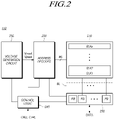
- FIG. 2 is a block diagram schematically illustrating a memory device according to an embodiment of the disclosed technology.
- FIG. 3 is a diagram illustrating a structure of word lines and bit lines of a memory device according to an embodiment of the disclosed technology.
- FIG. 4 is a schematic configuration diagram of the memory system according to embodiments of the disclosed technology.
- FIG. 5 is a configuration diagram of a map cache according to embodiments of the disclosed technology.
- FIG. 6 is a diagram illustrating the operation of caching target map data in the map cache according to embodiments of the disclosed technology.
- FIG. 7 is a flowchart illustrating an example of the operation of determining whether to cache target map data in the map cache according to embodiments of the disclosed technology.
- FIG. 8 is a diagram illustrating an example of an address value of target map data according to embodiments of the disclosed technology.
- FIG. 9 is a diagram illustrating the number of flags that can be simultaneously set in the flag set for the cache line according to embodiments of the disclosed technology.
- FIG. 10 is a flowchart illustrating an operation of determining whether to skip the operation of caching target map data in the map cache by the cache line control circuit according to embodiments of the disclosed technology.
- FIG. 11 is a diagram illustrating K flag sets controlled in parallel by the cache line control circuit according to embodiments of the disclosed technology.
- FIG. 12 is a diagram illustrating an example of determining the K value of FIG. 11 .
- FIG. 13 is a diagram illustrating an example of the cache line control circuit according to embodiments of the disclosed technology.
- FIG. 14 is a diagram illustrating a method of operating the memory system according to embodiments of the disclosed technology.
- FIG. 15 is a diagram illustrating the configuration of a computing system based on embodiments of the disclosed technology.
- FIG. 1 is a diagram illustrating the schematic configuration of a memory system 100 based on an embodiment of the disclosed technology.
- the memory system 100 may include a memory device 110 configured to store data, and a memory controller 120 configured to control the memory device 110 .
- the memory device 110 may include multiple memory blocks each including a predetermined number of memory cells for storing data.
- the memory device 110 may be configured to operate in response to control signals received from the memory controller 120 .
- Operations of the memory device 110 may include, for example, a read operation, a program operation (also referred to as a “write operation”), and an erasure operation.
- the memory cells in the memory device 110 are used to store data and may be arranged in a memory cell array.
- the memory cell array may be divided into memory blocks of memory cells and each block includes different pages of memory cells.
- a page of cells is the smallest memory unit that can be programmed (or written) and read, and the data stored in memory cells can be erased at the block level.
- the memory device 110 may be implemented as various types, such as a double data rate synchronous dynamic random access memory (DDR SDRAM), a low power double data rate fourth generation (LPDDR4) SDRAM, a graphics double data rate (GDDR) SDRAM, a low power DDR (LPDDR), a rambus dynamic random access memory (RDRAM), a NAND flash memory, a vertical NAND flash memory, a NOR flash memory, a resistive random access memory (RRAM), a phase-change memory (PRAM), a magnetoresistive random access memory (MRAM), a ferroelectric random access memory (FRAM), or a spin transfer torque random access memory (SU-RAM).
- DDR SDRAM double data rate synchronous dynamic random access memory
- LPDDR4 SDRAM low power double data rate fourth generation SDRAM
- GDDR SDRAM graphics double data rate SDRAM
- LPDDR low power DDR
- RDRAM rambus dynamic random access memory
- NAND flash memory a NAND flash memory
- vertical NAND flash memory a vertical
- the memory device 110 may be implemented in a three-dimensional array structure. Some embodiments of the disclosed technology are applicable to any type of flash memory devices having an electric charge storage layer.
- the electric charge storage layer may be formed of a conductive material, and such an electric charge storage layer can be called a floating gate.
- the electric charge storage layer may be formed of an insulating material, and such a flash memory device can be called a charge trap flash (CTF).
- CTF charge trap flash
- the memory device 110 may be configured to receive a command and an address from the memory controller 120 to access an area of the memory cell array selected using the address. That is, the memory device 110 may perform an operation corresponding to the received command on a memory area in the memory device having a physical address corresponding to the received address from the controller.
- the memory device 110 may perform, among others, a program operation, a read operation, and an erasure operation.
- the memory device 110 may write (“program”) data to the area selected by the address.
- the memory device 110 may read data from a memory area selected by the address.
- the erasure operation the memory device 110 may erase data stored in a memory area selected by the address.
- the memory controller 120 may control write (program), read, erasure, and background operations to be performed on the memory device 110 .
- the background operation may include operations that are implemented to optimize the overall performance of the memory device 110 , such as a garbage collection operation (GC), a wear leveling (WL) operation, and a bad block management (BBM) operation.
- GC garbage collection operation
- WL wear leveling
- BBM bad block management
- the memory controller 120 may control the operation of the memory device 110 at the request of a host. Alternatively, the memory controller 120 may control the operation of the memory device 110 even in absence of request from the host when it performs such a background operation of the memory device.
- the memory controller 120 and the host may be separate devices. In some implementations, the memory controller 120 and the host may be integrated in a single device. In the following description, as an example, the memory controller 120 and the host are separate devices.
- the memory controller 120 may include a memory interface 122 , a control circuit 123 , and a host interface 121 .
- the host interface 121 may be configured to provide an interface for communication with the host.
- control circuit 123 may receive the command through the host interface 121 and may perform an operation of processing the received command.
- the memory interface 122 may be directly or indirectly connected to the memory device 110 to provide an interface for communication with the memory device 110 . That is, the memory interface 122 may be configured to provide the memory device 110 and the memory controller 120 with an interface for the memory controller 120 to perform memory operations on the memory device 110 based on control signals and instructions from the control circuit 123 .
- the control circuit 123 may be configured to control the operation of the memory device 110 through the memory controller 120 .
- the control circuit 123 may include a processor 124 and a working memory 125 .
- the control circuit 123 may further include an error detection/correction circuit (ECC circuit) 126 .
- ECC circuit error detection/correction circuit
- the processor 124 may control the overall operation of the memory controller 120 .
- the processor 124 may perform a logical operation.
- the processor 124 may communicate with the host HOST through the host interface 121 .
- the processor 124 may communicate with the memory device 110 through the memory interface 122 .
- the processor 124 may be used to run a flash translation layer (FTL) to effectively manage the memory operations on the memory system 100 .
- FTL flash translation layer
- the processor 124 may translate a logical block address (LBA) provided by the host into a physical block address (PBA) through the FTL.
- LBA logical block address
- PBA physical block address
- the FTL may receive the LBA and translate the LBA into the PBA by using a mapping table.
- Typical address mapping methods may include a page mapping method, a block mapping method, and a hybrid mapping method.
- the processor 124 may be configured to randomize data received from the host to write the randomized data to the memory cell array. For example, the processor 124 may randomize data received from the host by using a randomizing seed. The randomized data is provided to the memory device 110 and written to the memory cell array.
- the processor 124 may be configured to derandomize data received from the memory device 110 during a read operation. For example, the processor 124 may derandomize data received from the memory device 110 by using a derandomizing seed. The derandomized data may be output to the host HOST.
- the processor 124 may execute firmware (FW) to control the operation of the memory controller 120 .
- firmware FW
- the processor 124 may control the overall operation of the memory controller 120 and, in order to perform a logical operation, may execute (drive) firmware loaded into the working memory 125 during booting.
- the firmware refers to a program or software stored on a certain nonvolatile memory and is executed inside the memory system 100 .
- the firmware may include various functional layers.
- the firmware may include at least one of a flash translation layer (FTL) configured to translate a logical address in the host HOST requests to a physical address of the memory device 110 , a host interface layer (HIL) configured to interpret a command that the host HOST issues to a data storage device such as the memory system 100 and to deliver the command to the FTL, and a flash interface layer (FIL) configured to deliver a command issued by the FTL to the memory device 110 .
- FTL flash translation layer
- HIL host interface layer
- FIL flash interface layer
- the firmware may be stored in the memory device 110 , and then loaded into the working memory 125 .
- the working memory 125 may store firmware, program codes, commands, or pieces of data necessary to operate the memory controller 120 .
- the working memory 125 may include, for example, at least one among a static RAM (SRAM), a dynamic RAM (DRAM), and a synchronous RAM (SDRAM) as a volatile memory.
- SRAM static RAM
- DRAM dynamic RAM
- SDRAM synchronous RAM
- the error detection/correction circuit 126 may be configured to detect and correct one or more erroneous bits in the data by using an error detection and correction code.
- the data that is subject to the error detection and correction may include data stored in the working memory 125 , and data retrieved from the memory device 110 .
- the error detection/correction circuit 126 may be implemented to decode data by using the error correction code.
- the error detection/correction circuit 126 may be implemented by using various decoding schemes. For example, a decoder that performs nonsystematic code decoding or a decoder that performs systematic code decoding may be used.
- the error detection/correction circuit 126 may detect one or more erroneous bits on a sector basis. That is, each piece of read data may include multiple sectors.
- a “sector” may refer to a data unit that is smaller than the smallest unit for read operations (e.g., page) of a flash memory. Sectors constituting each piece of read data may be mapped based addresses.
- the error detection/correction circuit 126 may calculate a bit error rate (BER) and determine whether the number of erroneous bits in the data is within the error correction capability sector by sector. For example, if the BER is higher than a reference value, the error detection/correction circuit 126 may determine that the erroneous bits in the corresponding sector are uncorrectable and the corresponding sector is marked “fail.” If the BER is lower than the reference value, the error detection/correction circuit 126 may determine that the corresponding sector is correctable and the corresponding sector can be marked “pass.”
- BER bit error rate
- the error detection/correction circuit 126 may perform error detection and correction operations successively on all read data. When a sector included in the read data is correctable, the error detection/correction circuit 126 may go on to the next sector to check as to whether an error correction operation is needed on the next sector. Upon completion of the error detection and correction operations on all the read data in this manner, the error detection/correction circuit 126 may identify which sector is deemed uncorrectable in the read data. The error detection/correction circuit 126 may provide information (e.g., address of uncorrectable sector) regarding the sectors deemed uncorrectable to the processor 124 .
- information e.g., address of uncorrectable sector
- the memory system 100 may also include a bus 127 to provide a channel between the constituent elements 121 , 122 , 124 , 125 , and 126 of the memory controller 120 .
- the bus 127 may include, for example, a control bus for delivering various types of control signals and commands, and a data bus for delivering various types of data.
- the above-mentioned constituent elements 121 , 122 , 124 , 125 , and 126 of the memory controller 120 are illustrated in FIG. 1 by way of example. It is noted that some of the above-mentioned constituent elements 121 , 122 , 124 , 125 , and 126 of the memory controller 120 may be omitted, or some of the above-mentioned constituent elements 121 , 122 , 124 , 125 , and 126 of the memory controller 120 may be integrated into a single element. In addition, in some implementations, one or more other constituent elements may be added to the above-mentioned constituent elements of the memory controller 120 .
- the memory device 110 will be described in more detail with reference to FIG. 2 .
- FIG. 2 is a block diagram schematically illustrating a memory device 110 based on an embodiment of the disclosed technology.
- the memory device 110 may include a memory cell array 210 , an address decoder 220 , a read/write circuit 230 , a control logic 240 , and a voltage generation circuit 250 .
- the memory cell array 210 may include multiple memory blocks BLK 1 -BLKz, where z is a natural number equal to or larger than 2.
- multiple word lines WL and multiple bit lines BL may be arranged in rows and columns, and multiple memory cells MC may be arranged.
- the multiple memory blocks BLK 1 -BLKz may be connected to the address decoder 220 through the multiple word lines WL.
- the multiple memory blocks BLK 1 -BLKz may be connected to the read/write circuit 230 through the multiple bit lines BL.
- Each of the multiple memory blocks BLK 1 -BLKz may include multiple memory cells.
- the multiple memory cells are nonvolatile memory cells.
- such nonvolatile memory cells may be arranged in a vertical channel structure.
- the memory cell array 210 may be configured as a memory cell array having a two-dimensional structure and, in some implementations, may be arranged in a three-dimensional structure.
- Each of the multiple memory cells included in the memory cell array 210 may store at least one bit of data.
- each of the multiple memory cells included in the memory cell array 210 may be a single-level cell (SLC) configured to store one bit of data per memory cell.
- each of the multiple memory cells included in the memory cell array 210 may be a multi-level cell (MLC) configured to store two bits of data per memory cell.
- each of the multiple memory cells included in the memory cell array 210 may be a triple-level cell (TLC) configured to store three bits of data per memory cell.
- each of the multiple memory cells included in the memory cell array 210 may be a quad-level cell (QLC) configured to store four bits of data.
- the memory cell array 210 may include multiple memory cells that are configured to store at least five bits of data per memory cell.
- the address decoder 220 , the read/write circuit 230 , the control logic 240 , and the voltage generation circuit 250 may operate as peripheral circuits configured to drive the memory cell array 210 .
- the address decoder 220 may be connected to the memory cell array 210 through the multiple word lines WL.
- the address decoder 220 may be configured to operate in response to commands and control signals of the control logic 240 .
- the address decoder 220 may receive addresses through an input/output buffer inside the memory device 110 .
- the address decoder 220 may be configured to decode a block address among the received addresses.
- the address decoder 220 may select at least one memory block based on the decoded block address.
- the address decoder 220 may receive a read voltage Vread and a pass voltage Vpass from the voltage generation circuit 250 .
- the address decoder 250 may apply the read voltage Vread to a selected word line WL inside a selected memory block, when applying the read voltage during a read operation, and may apply the pass voltage Vpass to the remaining non-selected word lines WL.
- the address decoder 220 may apply a verification voltage generated by the voltage generation circuit 250 to a selected word line WL inside a selected memory block, during a program verification operation, and may apply the pass voltage Vpass to the remaining non-selected word lines WL.
- the address decoder 220 may be configured to decode a column address among the received addresses.
- the address decoder 220 may transmit the decoded column address to the read/write circuit 230 .
- the memory device 110 may perform the read operation and the program operation on a page by page basis. Addresses received when the read operation and the program operation are requested may include at least one of a block address, a row address, and a column address.
- the address decoder 220 may select one memory block and one word line based on the block address and the row address.
- the column address may be decoded by the address decoder 220 and provided to the read/write circuit 230 .
- the address decoder 220 may include at least one of a block decoder, a row decoder, a column decoder, and an address buffer.
- the read/write circuit 230 may include multiple page buffers PB.
- the read/write circuit 230 may operate as a “read circuit” when the memory cell array 210 performs a read operation, and may operate as a “write circuit” when the memory cell array 210 performs a write operation.
- the above-mentioned read/write circuit 230 is also referred to as a page buffer circuit including multiple page buffers PB, or a data register circuit.
- the read/write circuit 230 may include a data buffer that can hold data for data processing and, in some implementations, may further include a cache buffer for data caching.
- the multiple page buffers PB may be connected to the memory cell array 210 through the multiple bit lines BL.
- the multiple page buffers PB may continuously supply a sensing current to the bit lines BL connected to the memory cells to detect, at a sensing node, a change in the amount of current that flows based on the program state of a corresponding memory cell, and may hold or latch the corresponding voltage as sensing data.
- the read/write circuit 230 may operate in response to page buffer control signals output from the control logic 240 .
- the read/write circuit 230 senses a voltage value of a memory cell and the voltage value is read out as data.
- the read/write circuit 230 temporarily stores the retrieved data, and outputs the data DATA to the input/output buffer of the memory device 110 .
- the read/write circuit 230 may include a column selection circuit, in addition to the page buffers PB or page registers.
- the control logic 240 may be connected to the address decoder 220 , the read/write circuit 230 , and the voltage generation circuit 250 .
- the control logic 240 may receive a command CMD and a control signal CTRL through the input/output buffer of the memory device 110 .
- the control logic 240 may be configured to control the overall operation of the memory device 110 in response to the control signal CTRL.
- the control logic 240 may output a control signal for adjusting the voltage level at sensing nodes of multiple page buffers PB.
- the control logic 240 may control the read/write circuit 230 to perform a read operation on the memory cells in the memory cell array 210 .
- the voltage generation circuit 250 may generate a read voltage Vread and a pass voltage Vpass, which are used during the read operation, in response to a voltage generation circuit control signal provided by the control logic 240 .
- a memory block BLK included in the memory device 110 may consist of multiple pages PG, each of which includes a plurality of memory cells.
- the plurality of memory cells can be arranged in multiple strings.
- the multiple pages PG can be mapped to multiple word lines WL, and the multiple strings STR can be mapped to multiple bit lines BL.
- multiple word lines WL and multiple bit lines BL may be arranged in rows and columns.
- each of the multiple word lines WL may be arranged in the row direction, and each of the multiple bit lines BL may be arranged in the column direction.
- each of the multiple word lines WL may be arranged in the column direction, and each of the multiple bit lines BL may be arranged in the row direction.
- the multiple word lines WL and the multiple bit lines BL may intersect with each other when viewed from above, thereby defining a memory array including multiple memory cells MC.
- Each memory cell MC may have a transistor TR arranged therein.
- the transistor TR arranged in each memory cell MC may include a drain, a source, and a gate.
- the drain (or source) of the transistor TR may be connected to the corresponding bit line BL directly or via another transistor TR.
- the source (or drain) of the transistor TR may be connected to the source line (which may be the ground) directly or via another transistor TR.
- the gate of the transistor TR may include a floating gate (FG) surrounded by an insulator, and a control gate (CG) to which a gate voltage is applied from a word line WL.
- a first selection line (also referred to as a source selection line or a drain selection line) may be additionally arranged outside the first outermost word line, which is closer to the read/write circuit 230 among two outermost word lines, and a second selection line (also referred to as a drain selection line or a source selection line) may be additionally arranged outside the other second outermost word line.
- At least one dummy word line may be additionally arranged between the first outermost word line and the first selection line. In addition, at least one dummy word line may be additionally arranged between the second outermost word line and the second selection line.
- a read operation and a program operation (write operation) of the memory block may be performed on a page by page basis, and an erasure operation may be performed on a memory block by memory block basis.
- FIG. 3 is a diagram illustrating a structure of word lines WL and bit lines BL of a memory device 110 based on an embodiment of the disclosed technology.
- the memory device 110 has a core area in which memory cells MC are concentrated, and an auxiliary area which corresponds to the remaining area other than the core area.
- the auxiliary area includes circuitry for supporting the operations of the memory cell array 210 .
- the core area may include pages PG and strings STR.
- multiple word lines WL 1 -WL 9 and multiple bit lines BL are arranged to intersect when viewed from above.
- the word lines WL 1 -WL 9 may be connected to a row decoder 310 .
- the bit lines BL may be connected to a column decoder 320 .
- a data register 330 which corresponds to the read/write circuit 230 of FIG. 2 , may exist between the multiple bit lines BL and the column decoder 320 .
- the multiple word lines WL 1 -WL 9 may correspond to multiple pages PG.
- each of the multiple word lines WL 1 -WL 9 may correspond to one page PG as illustrated in FIG. 3 .
- each of the multiple word lines WL 1 -WL 9 may correspond to at least two (e.g., two or four) pages PG.
- Each page PG is the smallest unit in connection with conducting a program operation and a read operation, and all memory cells MC within the same page PG may perform simultaneous operations when conducting a program operation and a read operation.
- the multiple bit lines BL may be connected to the column decoder 320 .
- the multiple bit lines BL may be divided into odd-numbered bit lines BL and even-numbered bit lines BL such that a pair of odd-numbered bit line BL and even-numbered bit line B are coupled in common to a column decoder 320 .
- the address may be used to access one or more memory cells MC in the core area.
- the address can be provided through the input/output end to the row decoder 310 and the column decoder 320 to select a corresponding target memory cell.
- the word “target memory cell” can be used to indicate one of the memory cells MC targeted to be accessed from the memory controller or the user, and in some implementations the memory cells MC may be located at intersections between the word lines WL 1 -WL 9 connected to the row decoder 310 and the bit lines BL connected to the column decoder 320 .
- the data register 330 plays an important role because all data processing by the memory device 110 , including program and read operations, occurs via the data register 330 . If data processing by the data register 330 is delayed, all of the other areas need to wait until the data register 330 finishes the data processing, degrading the overall performance of the memory device 110 .
- multiple transistors TR 1 -TR 9 may be connected to multiple word lines WL 1 -WL 9 , respectively.
- the multiple transistors TR 1 -TR 9 correspond to memory cells MC.
- the multiple transistors TR 1 -TR 9 include control gates CG and floating gates FG.
- the multiple word lines WL 1 -WL 9 include two outermost word lines WL 1 and WL 9 .
- a first selection line DSL may be additionally arranged outside the first outermost word line WL 1 , which is closer to the data register 330 and has a shorter signal path compared to the other outermost word line WL 9 .
- a second selection line SSL may be additionally arranged outside the other second outermost word line WL 9 .
- the first selection transistor D-TR which is controlled to turn on/off by the first selection line DSL, has a gate electrode connected to the first selection line DSL, but includes no floating gate FG.
- the second selection transistor S-TR which is controlled to turn on/off by the second selection line SSL, has a gate electrode connected to the second selection line SSL, but includes no floating gate FG.
- the first selection transistor D-TR is used as a switch circuit that connects the corresponding string STR to the data register 330 .
- the second selection transistor S-TR is used as a switch circuit that connects the corresponding string STR to the source line SL. That is, the first selection transistor D-TR and the second selection transistor S-TR can be used to enable or disable the corresponding string STR.
- the memory system 100 fills the target memory cell MC of the bit line BL which is to be programmed with electrons. Accordingly, the memory system 100 applies a predetermined turn-on voltage Vcc to the gate electrode of the first selection transistor D-TR, thereby turning on the first selection transistor D-TR, and applies a predetermined turn-off voltage (for example, 0V) to the gate electrode of the second selection transistor S-TR, thereby turning off the second selection transistor S-TR.
- Vcc predetermined turn-on voltage
- the memory system 100 turns on both of the first and second selection transistors D-TR and S-TR during a read operation or a verification operation. Accordingly, during a read operation or a verification operation, an electric current may flow through the corresponding string STR and drain to the source line SL, which corresponds to the ground voltage, such that the voltage level of the bit line BL can be measured. However, during a read operation, there may be a time difference in the on/off timing between the first selection transistor D-TR and the second selection transistor S-TR.
- the memory system 100 may apply a predetermined voltage (e.g., +20V) to the substrate through a source line SL during an erasure operation.
- a predetermined voltage e.g., +20V
- the memory system 100 applies a certain voltage to allow both the first selection transistor D-TR and the second selection transistor S-TR to float during an erasure operation.
- the applied erasure voltage can remove electrical charges from the floating gate FG of the selected memory cell.
- an inexecutable command can be generated due to an error in the firmware, and there is a probability for the memory controller to receive such an inexecutable command.
- the memory device does not respond to inform the memory controller that an inexecutable command has been generated, and thus the memory controller is unable to identify the causes of the malfunction when a memory system malfunctions due to an inexecutable command.
- the technology disclosed in this patent document can be implemented in various embodiments to identify that an inexecutable command has been issued for the memory device.
- a memory system 100 for implementing the disclosed technology may manage map data for performing an operation of reading, writing and erasing data in a memory device 100 .
- the memory system may include a special cache memory device as a map cache separate from the memory device for caching the map data to quickly access the map data without accessing the memory device 110 .
- this map cache may be part of the memory controller 120 .
- This map cache can be used to store certain data that is also stored in the memory device 110 and is known as a cache hit.
- a computer processor e.g., a CPU
- needs to access such data instead of going to the memory device 110 , such data can be accessed at a high speed from the map cache.
- a cache miss For data that is only stored in the memory device 110 but is not cached in the map cache, such data is a cache miss and can only be accessed by reading it from the memory device at a slower speed.
- the memory system can quickly access the map data, and can quickly process the operation of reading, writing and erasing data in the memory device.
- FIG. 4 is a schematic configuration diagram of a memory system 100 based on some embodiments of the disclosed technology.
- the memory controller 120 of the memory system 100 may include the map cache MAP_CACHE and the cache line control circuit CLCC.
- the map cache MAP_CACHE may include N cache lines CACHE_LINEs each used to cache map data (where N is a natural number equal to or greater than 2).
- the cache line CACHE_LINE refers to a basic unit of the map cache MAP_CACHE, and the map cache MAP_CACHE may cash the map data in the unit of the cache line CACHE_LINE.
- the map cache MAP_CACHE may cache map data in the unit of 64 byte, and thus map data having a size smaller than 64 byte, e.g., 32 byte, 16 byte, may not be cashed in the map cache MAP_CACHE.
- the memory controller 120 may access the map data in the map cache MAP_CACHE, and if the map data is not cached in the map cache MAP_CACHE, the memory controller 120 may read the map data from the memory device 110 and then cache the map data in the map cache MAP_CACHE.
- the map cache MAP_CACHE may be located in the working memory 125 of the memory controller 120 .
- the map cache MAP_CACHE may cache various types of map data.
- the types of map data that can be cached in the map cache MAP_CACHE are as follows.
- Map data having the L2V data type may indicate a mapping relationship between the logical address (LA) transmitted from the host and the virtual physical address (VA) of the memory device 100 .
- the virtual physical address may correspond to the physical address of the virtual flash memory, which may correspond to the physical address of the memory device 110 by the virtual flash layer.
- Map data having the VPT data type may indicate whether a page located at an address indicated by the map data is a valid page.
- Map data having the journaling data type may indicate changes in map data and be used to track a change history of map data.
- Map data having other data types than the L2V data, VPT data, and journaling data may indicate information (e.g. read count and erase count for each memory block).
- the cache line control circuit CLCC may control N flag sets corresponding to the N cache lines CACHE_LINE included in the map cache MAP_CACHE.
- the flag set corresponding to each cache line may include M flags indicating whether or not the cache hits have been made for each of the M data units.
- the map cache MAP_CACHE is checked to see if the requested item is in the map cache MAP_CACHE. If it is, it is called a cache “hit” and the item is retrieved from the map cache MAP_CACHE.
- the flag may indicate two states including a set state or a reset state.
- the set state may have a first value (e.g., 1) and the reset state may have a second value (e.g., 0).
- the configuration of the cache line and flag set will be described in detail below with reference to FIG. 5 .
- the flag set corresponding to the cache line CACHE_LINE may be located in the map cache MAP_CACHE together with the corresponding cache line, or may be located in the cache line control circuit CLCC separately from the corresponding cache line, or may be located in a separate volatile memory located outside the map cache MAP_CACHE and the cache line control circuit CLCC.
- the cache line control circuit CLCC may be a separate logic circuit located outside the processor 124 of the memory controller 120 .
- the cache line control circuit CLCC may be implemented with a combination of microprocessor, CPU, FPGA, ASIC and other programmable logic elements.
- FIG. 5 is a configuration diagram of the map cache MAP_CACHE according to embodiments of the disclosed technology.
- each of the N cache lines CACHE_LINE included in the map cache MAP_CACHE may include M data units DU 1 to DUM.
- Each flag set may include M flags F 1 to FM indicating whether or not the cache hits have been made for the M data units DU 1 to DUM that are included in the corresponding cache line.
- a flag may be set when the cache hit was occurred for the data unit and the memory controller 120 accesses the data unit.
- the flag F 1 corresponding to the data unit DU 1 may be set.
- the flag F 2 corresponding to the data unit DU 2 may be set.
- Each flag may be reset when the data unit corresponding to the flag is read or evicted from the map cache MAP_CACHE.
- the flag set FLG_SET described above may be implemented using various data structures.
- the flag set FLG_SET may be implemented as a bitmap. In this case, each bit included in the bitmap may correspond to one flag.
- the flag set FLG_SET may be implemented as a table. In this case, each table entry included in the table may correspond to one flag.
- the cache line control circuit CLCC determine the target map data TGT_MAP_DATA to be cached in the map cache MAP_CACHE based on a flag set FLG_SET for one of the N cache lines CACHE_LINE included in the map cache MAP_CACHE.
- FIG. 6 is a diagram illustrating the operation of caching target map data TGT_MAP_DATA in the map cache MAP_CACHE according to embodiments of the disclosed technology.
- the cache line control circuit CLCC may check the number of flags set in the flag set FLG_SET corresponding to the first cache line CACHE_LINE_ 1 among the N cache lines CACHE_LINE included in the map cache MAP_CACHE ( ⁇ circle around ( 1 ) ⁇ ). For example, in the case that the number of flags included in the flag set FLG_SET corresponding to the first cache line CACHE_LINE_ 1 is 8, the cache line control circuit CLCC may confirm that the set flags are 4.
- the cache line control circuit CLCC may determine whether to cache the target map data TGT_MAP_DATA ( ⁇ circle around ( 2 ) ⁇ ) based on the number of flags set in the flag set FLG_SET corresponding to the first cache line CACHE_LINE_ 1 .
- the target map data TGT_MAP_DATA may be cached in the map cache MAP_CACHE from the memory device 110 .
- the target map data TGT_MAP_DATA is map data determined to be highly likely to be accessed by the memory controller 120 by the cache line control circuit CLCC.
- the cache line control circuit CLCC may select target map data TGT_MAP_DATA from among map data stored in the memory device 110 .
- the cache line control circuit CLCC may read the target map data TGT_MAP_DATA from the memory device 110 and cache the target map data TGT_MAP_DATA in the second cache line CACHE_LINE_ 2 among the N cache lines CACHE_LINE included in the map cache MAP_CACHE ( ⁇ circle around ( 3 ) ⁇ ).
- the second cache line CACHE_LINE_ 2 is a cache line different from the first cache line CACHE_LINE_ 1 .
- the cache line control circuit CLCC may check the state of the flag set FLG_SET corresponding to the first cache line CACHE_LINE_ 1 , and cache target map data TGT_MAP_DATA, which is likely to be accessed by the memory controller 120 , in the map cache MAP_CACHE in advance before the access by the memory controller 120 .
- the memory controller 120 accesses the target map data TGT_MAP_DATA, the cache hit occurs in the map cache MAP_CACHE. Therefore, the memory controller 120 can access the target map data TGT_MAP_DATA in the second cache line CACHE_LINE_ 2 included in the map cache MAP_CACHE without having to search the target map data TGT_MAP_DATA from the memory device 110 . This can increase the hit ratio of the map cache MAP_CACHE.
- FIG. 7 is a flowchart illustrating an example of the operation of determining whether to cache target map data TGT_MAP_DATA in the map cache MAP_CACHE based on embodiments of the disclosed technology.
- the cache line control circuit CLCC may check the number A of flags set in the flag set corresponding to the first cache line CACHE_LINE_ 1 (S 710 ).
- the cache line control circuit CLCC may determine whether the value of A checked in step S 710 is equal to or greater than a threshold (S 720 ).
- the cache line control circuit CLCC may cache the target map data TGT_MAP_DATA in the second cache line CACHE_LINE_ 2 (S 730 ). If the value of A is less than the threshold (S 720 -N), the cache line control circuit CLCC may not cache the target map data TGT_MAP_DATA in the second cache line CACHE_LINE_ 2 (S 740 ).
- the cache line control circuit CLCC may cache the target map data TGT_MAP_DATA in the second cache line CACHE_LINE_ 2 when the number of flags set in the flag set corresponding to the first cache line CACHE_LINE_ 1 is equal to or greater than 5.
- the number (A) of flags set in the flag set corresponding to the first cache line CACHE_LINE_ 1 is compared with the threshold
- the set flag ratio can be obtained by dividing the value of A by the number of all flags included in the flag set.
- the set flag ratio can be compared with a threshold ratio value.
- the reason for determining whether to cache the target map data TGT_MAP_DATA in the map cache MAP_CACHE based on the number of flags set in the flag set FLG_SET is as follows.
- the memory controller 120 when the host sequentially reads or writes user data to the memory system 100 , the memory controller 120 has a high probability of accessing subsequent map data for the map data cached in the corresponding cache line after M data units included in one cache line cached in the map cache MAP_CACHE are sequentially hit. In this case, since the subsequent map data has not yet been accessed by the memory controller 120 , a cache miss may occur.
- VPT data among the map data can be sequentially accessed.
- the M data units included in one cache line in which the VPT data is cached in the map cache MAP_CACHE are sequentially hit, it is highly likely that subsequent map data for the map data cached in the corresponding cache line will be accessed.
- the cache line control circuit CLCC may check the number of flags set in the flag set corresponding to the corresponding cache line, and if the number of flags set is greater than or equal to the threshold, it may be determined that there is a high possibility that the subsequent map data following the map data cached in the corresponding cache line will be soon accessed by the memory controller 120 . Accordingly, the cache line control circuit CLCC may cache the subsequent map data in the map cache MAP_CACHE in advance so that a cache hit occurs when the subsequent map data is accessed. Therefore, the cache line control circuit CLCC can increase the hit ratio of the map cache MAP_CACHE and quickly process the request (e.g. read request/write request) received from the host.
- the request e.g. read request/write request
- FIG. 8 is a diagram illustrating an example of an address value of target map data TGT_MAP_DATA according to embodiments of the disclosed technology.
- map data cached in the first cache line CACHE_LINE_ 1 has an address value of A 0 is.
- Map data cached in the first cache line CACHE_LINE_ 1 may be stored in data units DU 1 to DUM.
- the map data stored in the address A 1 that is subsequent to the address A 0 may be determined as target map data TGT_MAP_DATA to be cached in the second cache line CACHE_LINE_ 2 .
- the map data cached in the first cache line CACHE_LINE_ 1 may be map data stored adjacent to the target map data TGT_MAP_DATA in the memory device 110 .
- the address A 1 and the address A 0 may be consecutive to each other.
- the value of A 1 may be determined based on the size of the cache line CACHE_LINE.
- the value of A 1 may be a value obtained by adding the size of the cache line CACHE_LINE to A 0 .
- the cache line control circuit CLCC may cache the target map data TGT_MAP_DATA adjacent to the map data cached in the first cache line CACHE_LINE_ 1 in the second cache line CACHE_LINE_ 2 .
- FIG. 9 is a diagram illustrating the number of flags that can be simultaneously set in the flag set FLG_SET for the cache line CACHE_LINE based on some embodiments of the disclosed technology.
- the cache line control circuit CLCC may determine the number of flags that are simultaneously set in the flag set based on a data access unit for the map cache MAP_CACHE.
- the data access unit for the map cache MAP_CACHE may be determined based on the size of map data that the memory controller 120 can access from the map cache MAP_CACHE at one time.
- the cache line control circuit CLCC may simultaneously set C flags in the flag set FLG_SET. For example, if the data unit DU is 4 byte and C is 8, the cache line control circuit CLCC may simultaneously set eight flags in the flag set FLG_SET.
- the cache line control circuit CLCC may set 1 flag in the flag set FLG_SET.
- FIG. 10 is a flowchart illustrating an operation of determining whether to skip the operation of caching target map data TGT_MAP_DATA in the map cache MAP_CACHE by the cache line control circuit CLCC according to embodiments of the disclosed technology.
- the cache line control circuit CLCC may search the target map data TGT_MAP_DATA to be cached in the map cache MAP_CACHE in the map cache MAP_CACHE (S 1010 ).
- the cache line control circuit CLCC may determine whether the target map data TGT_MAP_DATA has been previously cached in the map cache MAP_CACHE (S 1020 ). When the host randomly reads or writes user data to the memory system 100 , there is a possibility that the target map data TGT_MAP_DATA is already cached in the map cache MAP_CACHE.
- the cache line control circuit CLCC may skip the operation of caching the target map data TGT_MAP_DATA in the second cache line CACHE_LINE_ 2 (S 1030 ). This is because it is not necessary to cache the target map data TGT_MAP_DATA in duplicate in the map cache MAP_CACHE.
- the cache line control circuit CLCC may cache the target map data TGT_MAP_DATA in the second cache line CACHE_LINE_ 2 (S 1040 ).
- FIG. 11 is a diagram illustrating K flag sets controlled in parallel by the cache line control circuit CLCC according to embodiments of the disclosed technology.
- the cache line control circuit CLCC may control flag sets FLG_SET for a maximum of K cache lines (where K is a natural number less than N) among N cache lines CACHE_LINE included in the map cache MAP_CACHE in parallel.
- the feature that the cache line control circuit CLCC controls the flag sets FLG_SET for K cache lines in parallel may mean that the cache line control circuit CLCC may process an arbitrary flag set among the flag sets FLG_SET for K cache lines instead of sequentially processing the flag set for each cache line.
- the cache line control circuit CLCC may simultaneously control the flag sets FLG_SET for each of the K cache lines. For example, when the memory controller 120 simultaneously accesses a plurality of cache lines among N cache lines CACHE_LINE through different processes or threads, the cache line control circuit CLCC may control a plurality of flag sets corresponding to each of the plurality of cache lines being accessed.
- the cache line control circuit CLCC can quickly cache map data being required to be cached in advance in the map cache MAP_CACHE by controlling the plurality of flag sets in parallel instead of sequentially controlling.
- FIG. 12 is a diagram illustrating an example of determining the K value of FIG. 11 .
- the K value may be determined according to the number of types of map data capable of being cached in the N cache lines CACHE_LINE included in the map cache MAP_CACHE and the number of instances accessible to the N cache lines CACHE_LINE.
- the type of the map data may be an L2V data type or a VPT data type, for example.
- the instance may be a unit for performing the operation of accessing map data cached in the map cache MAP_CACHE, and may be a thread or a process.
- FTL can manage more than one instance.
- FIG. 12 it is assumed that there are two types of map data (L2V data type or VPT data type) that can be cached in N cache lines CACHE_LINE. In addition, it is assumed that the number of instances accessible to N cache lines CACHE_LINE is L.
- the K value may be (2*L), which is a product of 2 types of map data and L number of instances. This mean that up to (2*L) cache lines can be accessed at the same time when all instances accessible to N cache lines CACHE_LINE have access streams accessing two different types of map data.
- the cache line control circuit CLCC may include a flag set cache for caching flag sets for K cache lines.
- this will be described in detail in FIG. 13 .
- FIG. 13 is a diagram illustrating an example of the cache line control circuit CLCC according to embodiments of the disclosed technology.
- the cache line control circuit CLCC may cache the flag sets for K cache lines to be controlled in parallel among the N cache lines CACHE_LINE in the flag set cache FLG_SET_CACHE.
- the cache line control circuit CLCC may cache the corresponding flag set in the flag set cache FLG_SET_CACHE.
- the cache line control circuit CLCC may evict any one of the K flag sets already cached in the flag set cache FLG_SET_CACHE from the flag set cache FLG_SET_CACHE.
- the policy for eviction of any one of K flag sets already cached in the flag set cache FLG_SET_CACHE may be, for example, least recently used (LRU), least frequently used (LFU), or first in first out (FIFO).
- FIG. 14 is a diagram illustrating a method of operating the memory system 100 according to embodiments of the disclosed technology.
- the operating method of the memory system 100 may include the step of confirming N (N is a natural number of 2 or more) flag sets FLG_SET corresponding to each of the N cache lines CACHE_LINE capable of caching map data.
- Each flag set may include M flags indicating whether a cache hit for each of M (M is a natural number of 2 or more) data units included in the corresponding cache line (S 1410 ).
- the operation method of the memory system 100 may include the step of determining target map data TGT_MAP_DATA based on the number of flags set in the flag set corresponding to the first cache line CACHE_LINE_ 1 among the N cache lines CACHE_LINE (S 1420 ).
- the operating method of the memory system 100 may include the step of reading target map data TGT_MAP_DATA from the memory device 110 and caching it in a second cache line CACHE_LINE_ 2 among N cache lines CACHE_LINE (S 1430 ).
- step S 1430 when the number of flags set in the flag set corresponding to the first cache line CACHE_LINE_ 1 is equal to or greater than the threshold, the memory system 100 may cache the target map data TGT_MAP_DATA to the second cache line CACHE_LINE_ 2 .
- the address value of the target map data TGT_MAP_DATA may be the subsequent address value of the address of the map data cached in the first cache line CACHE_LINE_ 1 .
- the memory system 100 may check flag sets for a maximum of K cache lines (K is a natural number less than N) among N cache lines CACHE_LINE in parallel.
- the K value may be determined based on the number of types of map data capable of being cached in the N cache lines and the number of instances accessible to the N cache lines.
- the operation of the memory controller 120 described above may be controlled by the control circuit 123 , and may be performed in such a manner that the processor 124 executes or drives the firmware in which all operations of the memory controller 120 are programmed.
- FIG. 15 is a diagram illustrating the configuration of a computing system 1500 according to embodiments of the disclosed technology.
- the computing system 1500 may include: a memory system 100 electrically connected to a system bus 1560 ; a CPU 1510 configured to control the overall operation of the computing system 1500 ; a RAM 1520 configured to store data and information related to operations of the computing system 1500 ; a user interface/user experience (UI/UX) module 1530 configured to provide the user with a user environment; a communication module 1540 configured to communicate with an external device as a wired and/or wireless type; and a power management module 1550 configured to manage power used by the computing system 1500 .
- UI/UX user interface/user experience
- the computing system 1500 may be a personal computer (PC) or may include a mobile terminal such as a smartphone, a tablet or various electronic devices.
- PC personal computer
- mobile terminal such as a smartphone, a tablet or various electronic devices.
- the computing system 1500 may further include a battery for supplying an operating voltage, and may further include an application chipset, a graphic-related module, a camera image processor, and a DRAM. Other elements would be obvious to a person skilled in the art.
- the memory system 100 may include not only a device configured to store data in a magnetic disk such as a hard disk drive (HDD), but also a device configured to store data in a nonvolatile memory such as a solid state drive (SSD), a universal flash storage device, or an embedded MMC (eMMC) device.
- the non-volatile memory may include a read only memory (ROM), a programmable ROM (PROM), an electrically programmable ROM (EPROM), an electrically erasable and programmable ROM (EEPROM), a flash memory, a phase-change RAM (PRAM), a magnetic RAM (MRAM), a resistive RAM (RRAM), a ferroelectric RAM (FRAM), and the like.
- the memory system 100 may be implemented as storage devices of various types and mounted inside various electronic devices.
- the operation delay time of the memory system may be reduced or minimized.
- the disclosed technology can be implemented in a way that reduces or minimizes an overhead occurring in the process of calling a specific function.
Landscapes
- Engineering & Computer Science (AREA)
- Theoretical Computer Science (AREA)
- Physics & Mathematics (AREA)
- General Engineering & Computer Science (AREA)
- General Physics & Mathematics (AREA)
- Quality & Reliability (AREA)
- Read Only Memory (AREA)
- Memory System Of A Hierarchy Structure (AREA)
- Debugging And Monitoring (AREA)
- Techniques For Improving Reliability Of Storages (AREA)
Abstract
Description
Claims (13)
Applications Claiming Priority (2)
| Application Number | Priority Date | Filing Date | Title |
|---|---|---|---|
| KR1020200117455A KR20220035568A (en) | 2020-09-14 | 2020-09-14 | Memory system and operating method of memory system |
| KR10-2020-0117455 | 2020-09-14 |
Publications (2)
| Publication Number | Publication Date |
|---|---|
| US20220083471A1 US20220083471A1 (en) | 2022-03-17 |
| US11416401B2 true US11416401B2 (en) | 2022-08-16 |
Family
ID=80539286
Family Applications (1)
| Application Number | Title | Priority Date | Filing Date |
|---|---|---|---|
| US17/183,201 Active US11416401B2 (en) | 2020-09-14 | 2021-02-23 | Memory system and operating method thereof |
Country Status (3)
| Country | Link |
|---|---|
| US (1) | US11416401B2 (en) |
| KR (1) | KR20220035568A (en) |
| CN (1) | CN114185816B (en) |
Citations (11)
| Publication number | Priority date | Publication date | Assignee | Title |
|---|---|---|---|---|
| US20100332730A1 (en) * | 2009-06-30 | 2010-12-30 | Royer Jr Robert J | Method and system for managing a nand flash memory |
| KR101422557B1 (en) | 2006-05-29 | 2014-08-13 | 샌디스크 아이엘 엘티디 | Predictive data loader |
| US20170075813A1 (en) * | 2015-09-11 | 2017-03-16 | Kabushiki Kaisha Toshiba | Memory device and information processing device |
| US20170091104A1 (en) * | 2015-09-30 | 2017-03-30 | Arm Limited | Apparatus and method for prefetching |
| US20170364446A1 (en) * | 2016-06-15 | 2017-12-21 | HGST Netherlands B.V. | Compression and caching for logical-to-physical storage address mapping tables |
| KR20180124708A (en) | 2017-05-12 | 2018-11-21 | 삼성전자주식회사 | Apparatus including integrated confirmation queue circuit and operation method thereof |
| US20190155723A1 (en) * | 2017-11-21 | 2019-05-23 | SK Hynix Inc. | Data storage device and operating method thereof |
| US20190220416A1 (en) * | 2018-01-16 | 2019-07-18 | SK Hynix Inc. | Data storage apparatus and operating method thereof |
| US20190235762A1 (en) * | 2018-01-29 | 2019-08-01 | Toshiba Memory Corporation | Memory system controlling nonvolatile memory |
| US20200034298A1 (en) * | 2018-07-25 | 2020-01-30 | Western Digital Technologies, Inc. | Speculative pre-fetching of flash translation layer tables for use with solid state systems |
| US20200301847A1 (en) * | 2019-03-19 | 2020-09-24 | Toshiba Memory Corporation | Memory system for controlling nonvolatile memory |
Family Cites Families (3)
| Publication number | Priority date | Publication date | Assignee | Title |
|---|---|---|---|---|
| KR102252377B1 (en) * | 2017-11-20 | 2021-05-14 | 삼성전자주식회사 | A multi processor system and a method for managing data of processor included in the system |
| KR102675307B1 (en) * | 2018-04-24 | 2024-06-17 | 에스케이하이닉스 주식회사 | Storage device and operating method thereof |
| KR20200013897A (en) * | 2018-07-31 | 2020-02-10 | 에스케이하이닉스 주식회사 | Controller and operation method thereof |
-
2020
- 2020-09-14 KR KR1020200117455A patent/KR20220035568A/en active Pending
-
2021
- 2021-02-23 US US17/183,201 patent/US11416401B2/en active Active
- 2021-05-31 CN CN202110602002.8A patent/CN114185816B/en active Active
Patent Citations (11)
| Publication number | Priority date | Publication date | Assignee | Title |
|---|---|---|---|---|
| KR101422557B1 (en) | 2006-05-29 | 2014-08-13 | 샌디스크 아이엘 엘티디 | Predictive data loader |
| US20100332730A1 (en) * | 2009-06-30 | 2010-12-30 | Royer Jr Robert J | Method and system for managing a nand flash memory |
| US20170075813A1 (en) * | 2015-09-11 | 2017-03-16 | Kabushiki Kaisha Toshiba | Memory device and information processing device |
| US20170091104A1 (en) * | 2015-09-30 | 2017-03-30 | Arm Limited | Apparatus and method for prefetching |
| US20170364446A1 (en) * | 2016-06-15 | 2017-12-21 | HGST Netherlands B.V. | Compression and caching for logical-to-physical storage address mapping tables |
| KR20180124708A (en) | 2017-05-12 | 2018-11-21 | 삼성전자주식회사 | Apparatus including integrated confirmation queue circuit and operation method thereof |
| US20190155723A1 (en) * | 2017-11-21 | 2019-05-23 | SK Hynix Inc. | Data storage device and operating method thereof |
| US20190220416A1 (en) * | 2018-01-16 | 2019-07-18 | SK Hynix Inc. | Data storage apparatus and operating method thereof |
| US20190235762A1 (en) * | 2018-01-29 | 2019-08-01 | Toshiba Memory Corporation | Memory system controlling nonvolatile memory |
| US20200034298A1 (en) * | 2018-07-25 | 2020-01-30 | Western Digital Technologies, Inc. | Speculative pre-fetching of flash translation layer tables for use with solid state systems |
| US20200301847A1 (en) * | 2019-03-19 | 2020-09-24 | Toshiba Memory Corporation | Memory system for controlling nonvolatile memory |
Non-Patent Citations (1)
| Title |
|---|
| Xie et al. (Exploiting Internal Parallelism for Address Translation in Solid State Drives, pub. 2017), ACM Transactions on Storage vol. 0. pp. 31 (Year: 2017). * |
Also Published As
| Publication number | Publication date |
|---|---|
| US20220083471A1 (en) | 2022-03-17 |
| CN114185816B (en) | 2025-03-28 |
| KR20220035568A (en) | 2022-03-22 |
| CN114185816A (en) | 2022-03-15 |
Similar Documents
| Publication | Publication Date | Title |
|---|---|---|
| US11755248B2 (en) | Memory system and operating method of memory system | |
| US12455787B2 (en) | Memory system and operating method thereof | |
| US11941272B2 (en) | Memory system and operating method of memory system | |
| US20240211153A1 (en) | Memory system for executing a target operation based on a program state of a super memory block and operating method thereof | |
| US11301174B2 (en) | Memory system, memory controller and method for operating memory system | |
| US20250117327A1 (en) | Memory system, memory controller and operating method of the memory system for controlling garbage collection | |
| US11327902B2 (en) | Memory system, memory controller, and operation method of memory system for setting lock on map segments cached in map cache | |
| US11675712B2 (en) | Memory system, memory controller, and operation method of memory system | |
| US20210382655A1 (en) | Memory device, memory system, and operation method of memory device | |
| US11669266B2 (en) | Memory system and operating method of memory system | |
| CN116136738A (en) | Memory system for performing background operation using external device and operating method thereof | |
| US12332788B2 (en) | System setting including operating frequency of random access memory based on cache hit ratio and operating method thereof | |
| US12099751B2 (en) | Memory system, memory controller and operating method of the memory system operating as read boost mode | |
| US20230221895A1 (en) | Memory system and operating method of memory system storing doorbell information in the buffer memory | |
| US12422996B2 (en) | Controller for controlling one-time programmable memory, system, and operation method thereof | |
| US11893255B2 (en) | Memory system for managing data corresponding to a plurality of zones and operating method thereof | |
| US11636007B2 (en) | Memory system and operating method thereof for flushing data in data cache with parity | |
| US11507509B2 (en) | Memory system, memory controller and method for operating memory system for determining whether to perform direct write based on reference write size | |
| US11416401B2 (en) | Memory system and operating method thereof | |
| US12197764B2 (en) | Memory system and operating method thereof | |
| US11822819B2 (en) | Memory system and operating method thereof | |
| US12346250B2 (en) | Controller and operating method thereof |
Legal Events
| Date | Code | Title | Description |
|---|---|---|---|
| AS | Assignment |
Owner name: SK HYNIX INC., KOREA, REPUBLIC OF Free format text: ASSIGNMENT OF ASSIGNORS INTEREST;ASSIGNOR:KIM, DO HUN;REEL/FRAME:055377/0808 Effective date: 20210121 |
|
| FEPP | Fee payment procedure |
Free format text: ENTITY STATUS SET TO UNDISCOUNTED (ORIGINAL EVENT CODE: BIG.); ENTITY STATUS OF PATENT OWNER: LARGE ENTITY |
|
| STPP | Information on status: patent application and granting procedure in general |
Free format text: NON FINAL ACTION MAILED |
|
| STPP | Information on status: patent application and granting procedure in general |
Free format text: RESPONSE TO NON-FINAL OFFICE ACTION ENTERED AND FORWARDED TO EXAMINER |
|
| STPP | Information on status: patent application and granting procedure in general |
Free format text: NOTICE OF ALLOWANCE MAILED -- APPLICATION RECEIVED IN OFFICE OF PUBLICATIONS |
|
| STPP | Information on status: patent application and granting procedure in general |
Free format text: PUBLICATIONS -- ISSUE FEE PAYMENT VERIFIED |
|
| STCF | Information on status: patent grant |
Free format text: PATENTED CASE |
|
| MAFP | Maintenance fee payment |
Free format text: PAYMENT OF MAINTENANCE FEE, 4TH YEAR, LARGE ENTITY (ORIGINAL EVENT CODE: M1551); ENTITY STATUS OF PATENT OWNER: LARGE ENTITY Year of fee payment: 4 |