US11412201B2 - Calibrated photo-detecting apparatus and calibration method thereof - Google Patents
Calibrated photo-detecting apparatus and calibration method thereof Download PDFInfo
- Publication number
- US11412201B2 US11412201B2 US17/033,640 US202017033640A US11412201B2 US 11412201 B2 US11412201 B2 US 11412201B2 US 202017033640 A US202017033640 A US 202017033640A US 11412201 B2 US11412201 B2 US 11412201B2
- Authority
- US
- United States
- Prior art keywords
- calibration data
- data
- calibration
- photo
- detecting apparatus
- Prior art date
- Legal status (The legal status is an assumption and is not a legal conclusion. Google has not performed a legal analysis and makes no representation as to the accuracy of the status listed.)
- Active, expires
Links
Images


Classifications
-
- G—PHYSICS
- G01—MEASURING; TESTING
- G01S—RADIO DIRECTION-FINDING; RADIO NAVIGATION; DETERMINING DISTANCE OR VELOCITY BY USE OF RADIO WAVES; LOCATING OR PRESENCE-DETECTING BY USE OF THE REFLECTION OR RERADIATION OF RADIO WAVES; ANALOGOUS ARRANGEMENTS USING OTHER WAVES
- G01S17/00—Systems using the reflection or reradiation of electromagnetic waves other than radio waves, e.g. lidar systems
- G01S17/88—Lidar systems specially adapted for specific applications
- G01S17/89—Lidar systems specially adapted for specific applications for mapping or imaging
- G01S17/894—Three-dimensional [3D] imaging with simultaneous measurement of time-of-flight at a two-dimensional [2D] array of receiver pixels, e.g. time-of-flight cameras or flash lidar
-
- H—ELECTRICITY
- H04—ELECTRIC COMMUNICATION TECHNIQUE
- H04N—PICTORIAL COMMUNICATION, e.g. TELEVISION
- H04N13/00—Stereoscopic video systems; Multi-view video systems; Details thereof
- H04N13/20—Image signal generators
- H04N13/204—Image signal generators using stereoscopic image cameras
- H04N13/246—Calibration of cameras
-
- G—PHYSICS
- G01—MEASURING; TESTING
- G01S—RADIO DIRECTION-FINDING; RADIO NAVIGATION; DETERMINING DISTANCE OR VELOCITY BY USE OF RADIO WAVES; LOCATING OR PRESENCE-DETECTING BY USE OF THE REFLECTION OR RERADIATION OF RADIO WAVES; ANALOGOUS ARRANGEMENTS USING OTHER WAVES
- G01S7/00—Details of systems according to groups G01S13/00, G01S15/00, G01S17/00
- G01S7/48—Details of systems according to groups G01S13/00, G01S15/00, G01S17/00 of systems according to group G01S17/00
- G01S7/483—Details of pulse systems
- G01S7/486—Receivers
- G01S7/4865—Time delay measurement, e.g. time-of-flight measurement, time of arrival measurement or determining the exact position of a peak
- G01S7/4866—Time delay measurement, e.g. time-of-flight measurement, time of arrival measurement or determining the exact position of a peak by fitting a model or function to the received signal
-
- G—PHYSICS
- G01—MEASURING; TESTING
- G01S—RADIO DIRECTION-FINDING; RADIO NAVIGATION; DETERMINING DISTANCE OR VELOCITY BY USE OF RADIO WAVES; LOCATING OR PRESENCE-DETECTING BY USE OF THE REFLECTION OR RERADIATION OF RADIO WAVES; ANALOGOUS ARRANGEMENTS USING OTHER WAVES
- G01S7/00—Details of systems according to groups G01S13/00, G01S15/00, G01S17/00
- G01S7/48—Details of systems according to groups G01S13/00, G01S15/00, G01S17/00 of systems according to group G01S17/00
- G01S7/497—Means for monitoring or calibrating
-
- G—PHYSICS
- G06—COMPUTING OR CALCULATING; COUNTING
- G06T—IMAGE DATA PROCESSING OR GENERATION, IN GENERAL
- G06T19/00—Manipulating three-dimensional [3D] models or images for computer graphics
- G06T19/20—Editing of three-dimensional [3D] images, e.g. changing shapes or colours, aligning objects or positioning parts
-
- H—ELECTRICITY
- H04—ELECTRIC COMMUNICATION TECHNIQUE
- H04N—PICTORIAL COMMUNICATION, e.g. TELEVISION
- H04N13/00—Stereoscopic video systems; Multi-view video systems; Details thereof
- H04N13/20—Image signal generators
- H04N13/204—Image signal generators using stereoscopic image cameras
- H04N13/243—Image signal generators using stereoscopic image cameras using three or more two-dimensional [2D] image sensors
Definitions
- Image sensors are widely used in many electronic devices such as a digital still camera, a smart phone, a video camera, a vehicle camera or a camera drone. More and more electronic devices are equipped with 2-dimensional (2D) and 3-dimensional (3D) image sensors, which include a plurality of photodetectors for performing optical-to-electrical conversion.
- 2D 2-dimensional
- 3D 3-dimensional
- Time-of-Flight (ToF) sensor is one kind of 3D image sensors, which measures a depth by correlating the phase delay between a modulated signal transmitted by a transmitter and a reflected modulated signal received by a receiver, where the receiver includes a plurality of photodetectors.
- the receiver includes a plurality of photodetectors.
- several non-ideal factors e.g., mismatch or dark current
- mismatch or dark current existed in the plurality of the photodetectors will affect the sensing accuracy of the ToF sensor, which may cause the erroneous results on the depth measurement. Therefore, there is a need for providing a calibrated photo-detecting apparatus and proving a calibration method for the photo-detecting apparatus.
- a photo-detecting apparatus includes an image sensor having a plurality of 3D photodetectors, configured to output a raw data; and a 3D image generator having a storage medium storing a calibration data, configured to output a 3D image based on the raw data and the calibration data; wherein the calibration data includes an IQ-mismatch calibration data, a non-linearity calibration data, a temperature calibration data or an offset calibration data.
- a calibration method includes providing an image sensor having a plurality of 3D photodetectors and outputting a raw data; and providing a 3D image generator having a storage medium storing a calibration data and outputting a 3D image based on the raw data and the calibration data; wherein the calibration data includes an IQ-mismatch calibration data, a non-linearity calibration data, a temperature calibration data or an offset calibration data.
- FIG. 1 illustrates a diagram of a photo-detecting apparatus, according to some embodiments.
- FIG. 2 illustrates a timing diagram of a ToF application, according to some embodiments.
- FIG. 3A illustrates a flowchart of generating the calibration data, according to some embodiments.
- FIG. 3B illustrates an IQ-mismatch model, according to some embodiments.
- FIG. 3C illustrates an IQ-mismatch calibration data, according to some embodiments.
- FIG. 3D illustrates a non-linear model, according to some embodiments.
- FIG. 3E illustrates a non-linear calibration data, according to some embodiments.
- FIG. 3F illustrates a temperature model, according to some embodiments.
- FIG. 3G illustrates a temperature calibration data, according to some embodiments.
- FIG. 3H illustrates a global offset model, according to some embodiments.
- FIG. 3I illustrates a global offset calibration data, according to some embodiments.
- FIG. 3J illustrates a pixel offset model, according to some embodiments.
- FIG. 3K illustrates a pixel offset calibration data, according to some embodiments.
- FIG. 4 illustrates a flowchart of generating the calibration data, according to some embodiments.
- FIG. 5 illustrates a diagram of a photo-detecting apparatus, according to some embodiments.
- FIG. 6 illustrates a circuit diagram of a temperature sensor, according to some embodiments.
- FIG. 7A illustrates a circuit diagram of a 3D photodetector, according to some embodiments.
- FIG. 7B illustrates a timing diagram of a 3D photodetector, according to some embodiments.
- FIG. 8 illustrates a diagram of a controller in connection with a temperature sensor and a 3D photodetector, according to some embodiments.
- FIG. 9A illustrates a diagram of a photo-detecting apparatus, according to some embodiments.
- FIG. 9B illustrates a diagram of an image sensor, according to some embodiments.
- FIG. 9C illustrates a diagram of an image sensor, according to some embodiments.
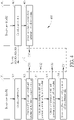
- FIG. 1 illustrates a diagram of a photo-detecting apparatus 100 .
- the photo-detecting apparatus 100 includes an image sensor 104 , a calibration data generator 106 and a 3D image generator 108 .
- the Image sensor 104 includes a plurality of 3D photodetectors 111 to collectively form a pixel array 104 - 1 .
- the image sensor 104 is configured to generate raw data R 1 through the pixel array 104 - 1 .
- the calibration data generator 106 is configured to generate calibration data C 1 to the 3D image generator 108 , where the 3D image generator 108 is configured to generate a 3D image IM according to the raw data R 1 and the calibration data C 1 .
- the calibration data C 1 may be stored at a storage medium 108 - 1 (e.g., register or flash memory).
- the calibration data C 1 can be referenced by the 3D image generator 108 as a look-up table during operation.
- the 3D image generator 108 can be implemented by digital processor (DSP), general purpose processor, application-specific integrated circuit (ASIC), digital circuitry, software module, or any combinations thereof.
- the photo-detecting apparatus 100 can be implemented in electronic devices such as a digital still camera, a smart phone, a video camera, a vehicle camera or a camera drone.
- the calibration data generator 106 can be a non-portable equipment (e.g., a lab equipment) and the calibration data C 1 can be pre-stored into the storage medium 108 - 1 before the production of the electronic devices, the electronic devices may not include the calibration data generator 106 therein.
- the calibration data generator 106 is an element which will not be implemented into the end product.
- FIG. 2 illustrates a timing diagram of a ToF application.
- Transmitting signal TX is a signal transmitted from a transmitter, which in this example is a square wave modulation signal.
- Receiving signal RX is a signal received by the image sensor 104 , where the receiving signal RX is the transmitting signal TX reflected from a target object (e.g., face or fingerprint).
- a target object e.g., face or fingerprint
- Demodulation signal DM in this example is also a square wave signal, configured to control the 3D photodetectors 111 of the image sensor 104 , including four phases, where a first phase DM 1 represents 0-degree, a second phase DM 2 represents 180-degree, a third phase DM 3 represents 90-degree and a fourth phase DM 4 represents 270-degree from the transmitting signal TX. These four phases will be applied to the 3D photodetectors 111 in turn.
- the demodulation signal DM applies the first phase DM 1 to control the 3D photodetectors 111 at a first time frame, applies the second phase DM 2 to control the 3D photodetectors 111 at a second time frame, applies the third phase DM 3 to control the 3D photodetectors 111 at a third time frame, and applies the fourth phase DM 4 to control the 3D photodetectors 111 at a fourth time frame.
- Four-phase demodulation signal DM is just an example, and one may use other numbers of phase as a demodulation signal to control the 3D photodetectors 111 .
- the image sensor 104 is configured to output the raw data R 1 to the calibration data generator 106 and 3D image generator 108 , where the raw data R 1 includes at least one or more phase-difference data Q 1 , Q 2 , Q 3 and Q 4 .
- these phase-difference data Q 1 , Q 2 , Q 3 and Q 4 relate to the phase-difference between the receiving signal RX and demodulation signal DM (or transmitting signal TX), as shown in FIG. 2 .
- FIG. 3A illustrates a flowchart 300 generating the calibration data C 1 , which is performed by the calibration data generator 106 .
- the calibration items include IQ-mismatch, non-linearity, temperature and offset, and example steps of generating the calibration data C 1 as show below:
- Step 301 receive the raw data R 1 .
- Step 302 calculate one or more parameters according to the raw data R 1 .
- Step 303 obtain an IQ-mismatch model and generate an IQ-mismatch calibration data C 11 according to the one or more parameters.
- Step 305 obtain a temperature model and generate a temperature calibration data C 13 according to the one or more parameters.
- Step 306 obtain an offset model and generate an offset calibration data C 14 according to the one or more parameters.
- one or multiple parameters may be obtained, such as an I-value V I , a Q-value V Q , a pixel intensity A, a phase delay ⁇ and a distance DIS.
- V Q ( Q 4 ⁇ Q 3)
- A ( V Q 2 +V I 2 ) 1/2
- Steps 303 to 306 are the steps to generate the IQ-mismatch calibration data C 11 , non-linearity C 12 , temperature calibration data C 13 and offset calibration data C 14 , respectively. These steps will be introduced below and in connection with FIG. 3B to FIG. 3K .
- the IQ-mismatch model and the IQ-mismatch calibration data C 11 are generated according to the one or more parameters generated in Step 302 .
- I-value V I is equal to Q-value V Q .
- this mismatch will cause a depth error D ERR1 .
- the depth error D ERR1 indicates the difference between the measured depth and the actual depth. For example, when actual depth is 130 cm and measured depth is 130.3 cm, the depth error D ERR1 is 0.3 cm.
- an IQ-mismatch model has to be established.
- FIG. 3B An example of the IQ-mismatch model can refer to FIG. 3B .
- the depth error D ERR1 caused by IQ-mismatch will be varied in accordance with the actual depth.
- this IQ-mismatch model can be obtained by experiment.
- the IQ-mismatch calibration data C 11 can be obtained according the IQ-mismatch model.
- FIG. 3C illustrates an example of the IQ-mismatch calibration data C 11 , which corresponds to the IQ-mismatch model illustrated in FIG. 3B .
- the IQ-mismatch calibration data C 11 can be written into the storage medium 108 - 1 to form a look-up table inside the 3D image generator 108 , such that the 3D image generator 108 can generate the 3D image IM based on the raw data R 1 and the IQ-mismatch calibration data C 11 stored in the storage medium 108 - 1 .
- FIG. 3D An example of the non-linearity model can refer to FIG. 3D .
- a curve Curve 1 illustrated in FIG. 3D represents an ideal relationship between the measured depth and the actual depth.
- a curve Curve 2 represents a non-ideal relationship between the measured depth and the actual depth when a non-linear error occurs.
- the depth error D ERR2 which is the difference between Curve 1 and Curve 2 , caused by non-linearity will be varied in accordance with the actual depth.
- this non-linearity model can be obtained by experiment.
- the non-linearity calibration data C 12 can be obtained according the non-linearity model.
- 3E illustrates an example of the non-linearity calibration data C 12 , which corresponds to the non-linearity model illustrated in FIG. 3D .
- the non-linearity calibration data C 12 can be written into the storage medium 108 - 1 to form a look-up table inside the 3D image generator 108 , such that the 3D image generator 108 can generate the 3D image IM based on the raw data R 1 and the non-linearity calibration data C 12 stored in the storage medium 108 - 1 .
- the temperature model and the temperature calibration data C 13 are generated according to the one or more parameters generated in Step 302 .
- Temperature is a factor causing depth error D ERR3 .
- FIG. 3F illustrates a temperature model according to an embodiment.
- the depth error D ERR3 is proportional to the temperature (i.e., higher temperature leads to a higher depth error D ERR3 ).
- the temperature calibration data C 13 as illustrated in FIG. 3G can be generated and written into the storage medium 108 - 1 to form a look-up table inside the 3D image generator 108 .
- the 3D image generator 108 can generate the 3D image IM based on the raw data R 1 and the temperature calibration data C 13 stored in the storage medium 108 - 1 .
- the offset model and the offset calibration data C 14 are generated according to the one or more parameters generated in Step 302 .
- Global offset is caused by signal delay inside a system and pixel offset is caused by manufacturing tolerance. Since global offset is a systematic offset, all the pixels can be compensated by the same value.
- Pixel offset is an offset that occurs in each pixel, and can be compensated per pixel.
- a system may perform steps 303 and 305 first, and then perform steps 304 and 306 .
- the steps 303 , 304 , 305 and 306 can be performed in parallel.
- a system may perform part of steps (e.g., performing steps 303 and 304 but not performing steps 305 and 306 ), instead of performing all the steps 303 , 304 , 305 and 306 .
- the 3D image generator 108 can execute these calibrations by the sequence of IQ-mismatch calibration data C 11 , non-linearity calibration data C 12 , temperature calibration data C 13 and offset calibration data C 14 during operation. In some other embodiments, the 3D image generator 108 can execute these calibrations by other sequences or execute part of these calibrations during operations.
- the calibration data generator 106 receives the raw data R 2 (e.g., image amplitude generated under active lighting or image intensity generated under passive NIR lighting) through the image sensor 104 and generates the parameters (e.g., focal lengths, principal point, radial distortion coefficients, tangential distortion coefficients) in step 402 .
- the calibration data generator 106 obtains the lens distortion model and generates the lens calibration data C 15 to the storage medium 108 - 1 based on the one or more parameters generated in step 402 .
- the one or more parameters generated in step 402 can be used in the steps 303 , 304 , 305 or 306 as a reference.
- the embodiments disclosed in FIG. 1 to FIG. 4 are the calibrations at the system level, which is for example performed by the 3D image generator 108 and improves the sensing quality and accuracy.
- the present disclosure further provides configurable 3D photodetector 111 to have different settings based on environmental temperature. As such, the operation of the 3D photodetector 111 can be optimized.
- FIG. 5 illustrates a diagram of a photo-detecting apparatus 500 .
- the photo-detecting apparatus 500 further includes a temperature sensor 110 and a controller 112 .
- the temperature sensor 110 is configured to sense an environmental temperature to generate a temperature information T 1 .
- the controller 112 is configured to output a control signal C 2 to control the configurations of the image sensor 104 according to the temperature information T 1 .
- FIG. 6 illustrates an example circuit diagram of the temperature sensor 110 .
- the temperature sensor 110 includes a reference current generator 602 , a sensing resistor Rsen and an analog-to-digital convertor ADC.
- the reference current generator 602 is configured to generate a reference current Iref 1 and a reference Iref 2 .
- the structure and connection of reference current generator 602 as illustrated in FIG. 6 including an operational amplifier OP, a transistor M 1 , a transistor M 2 and a reference resistor Rref.
- the reference resistor Rref is an external resistor, receiving a reference voltage Vref to generate the reference current Iref 1 .
- the reference currents Iref 1 and Iref 2 will be precise as well, which means the reference currents Iref 1 and Iref 2 are substantially independent of process, voltage and temperature.
- the reference current Iref 2 is mirrored from the reference current Iref 1 according to the aspect ratios of the transistors M 1 and M 2 , the reference current Iref 2 could be the same as the reference current Iref 1 , or could have a predetermined ratio of the reference current Iref 1 .
- the sensing voltage Vsen is also varied according to the environmental temperature.
- the temperature information T 1 which is a digital data, reflects the environmental temperature and will be outputted to the controller 112 .
- the analog-to-digital convertor ADC can be SAR-ADC, pipeline-ADC, flash-ADC or any other types of ADC.
- FIG. 7A illustrates a circuit diagram of the 3D photodetector 111 inside the image sensor 104 .
- the 3D photodetector 111 is configured to perform 3D sensing, including an optical-to-electric converter 170 , cascode transistors 130 A and 130 B, reset transistors 141 A and 141 B, capacitors 150 A and 150 B, source-follower transistors 142 A and 142 B, row-select transistors 143 A and 143 B and bit-lines BLA and BLB.
- the cascode transistor 130 A includes a first end coupled to the capacitor 150 A, a second end coupled to a collection terminal 111 C, and a control end for receiving a control signal VC 1 .
- the reset transistor 141 A includes a first end coupled to a supply voltage VDD 1 , a second end coupled to the capacitor 150 A, and a control end for receiving a reset signal RST.
- the source-follower transistor 142 A includes a first end coupled to a supply voltage VDD 2 , a second end, and a control end coupled to the capacitor 150 A.
- the cascode transistor 130 B includes a first end coupled to the capacitor 150 B, a second end coupled to a collection terminal 111 D, and a control end for receiving a control signal VC 2 .
- the reset transistor 141 B includes a first end coupled to the supply voltage VDD 1 , a second end coupled to the capacitor 150 B, and a control end for receiving the reset signal RST.
- the source-follower transistors 142 B includes a first end coupled to the supply voltage VDD 2 , a second end, and a control end coupled to the capacitor 150 B.
- the row-select transistor 143 B includes a first end coupled to the second end of the source-follower transistors 142 B, a second end coupled to the bit line BLB, and a control end for receiving a select signal SelB.
- the capacitor 150 B includes a first end coupled to the first end of the cascode transistor 130 B and a second end coupled to the ground voltage GND, where an output voltage VOUT 2 is generated on the first end of the capacitor 150 B. Furthermore, the capacitance of the capacitor 150 B can be adjusted by a configuration signal CB.
- the optical-to-electric converter 170 is configured to convert an incident light IL to the photo-currents 111 S 3 and 111 S 4 at collection terminals 111 C and 111 D, and output the photo-currents 111 S 3 and 111 S 4 to the cascode transistors 130 A and 130 B according to the demodulation signals 111 S 1 and 111 S 2 inputted to the demodulation terminals 111 A and 111 B.
- the photo-current 111 S 3 will be generated.
- the photo-current 111 S 4 will be generated.
- the 3D image generator 108 will determine the depth of the image according to the output voltages VOUT 1 and VOUT 2 .
- the demodulation signals 111 S 1 and 111 S 2 are square wave signals and collectively form a differential signal.
- one of the demodulation signals 111 S 1 and 111 S 2 can be the demodulation signal DM illustrated in FIG. 2 .
- the output voltages VOUT 1 and VOUT 2 will be read out onto the bit-lines BLA and BLB, respectively.
- the optical integration time Ti or the reset frequency 1/(Ti+Td) of the reset signal RST can be adjusted according to the environmental temperature.
- a plurality of subframes (labeled by Subframe 1 , Subframe 2 , etc.) will be generated to obtain a final frame during operation.
- the final 3D frame can be obtained according to an average of these subframes, an average of particular subframes, or providing different weighting for each subframe.
- the numbers of subframes can be dynamically adjusted according to the environmental temperature, or the rates of subframes can be dynamically adjusted according to the environmental temperature.
- FIG. 8 illustrates a diagram of the controller 112 in connection with the temperature sensor 110 and 3D photodetector 111 .
- the controller 112 is configured to set the configurations of the 3D photodetector 111 according to the analog-to-digital convertor ADC output signal, which represents the temperature information T 1 .
- the analog-to-digital convertor ADC output is 3-bit, the environmental temperature can be split into 8 ranges, as illustrated in FIG. 8 .
- the controller 112 is configured to generate the control signal C 2 , including configuration signals CA, CB, FCS, TCS, and/or VCS.
- the configuration signal CA is configured to adjust the capacitance of the capacitor 150 A
- the configuration signal CB is configured to adjust capacitance of the capacitor 150 B
- the configuration signal FCS is configured to adjust the frequency of the reset signal RST
- the configuration signal TCS is configured to adjust the optical integration time Ti
- the configuration signal VCS is configured to adjust the supply voltage VDD 1 .
- the controller 112 can be implemented by DSP processor, general purpose processor, application-specific integrated circuit (ASIC), digital circuitry, look-up-table or any combinations thereof.
- control signal C 2 may further includes a configuration signal (which is not shown in figure) configured to set the numbers of subframes and/or a configuration signal (which is not shown in figure) configured to set the rates of subframes.
- mapping relationship between the temperature information T 1 and control signal C 2 there is a mapping relationship between the temperature information T 1 and control signal C 2 .
- the configuration signals CA and CB will be Value 1
- the configuration signal FCS will be F 1
- the configuration signal TCS will be TC 1
- the configuration signal VCS will be value V 1 .
- Other mapping relationship between the temperature information T 1 and control signal C 2 can refer to the FIG. 8 , and the descriptions are hereby omitted.
- FIG. 9A illustrates a diagram of a photo-detecting apparatus 900 .
- the photo-detecting apparatus 900 further includes a pixel array 104 - 2 including a plurality of 2D photodetectors 114 .
- the pixel array 104 - 2 is configured to perform 2D sensing and generate a 2D image.
- FIG. 9B illustrates a diagram of the image sensor 104 , including the pixel array 140 - 1 for performing 3D sensing and the pixel array 140 - 2 for performing 2D sensing.
- the 3D photodetector 111 includes the substrate 160 and the light absorption material 180 formed on the substrate 160 , where the light absorption material 180 is different from the material of the substrate 160 .
- the light absorption material 180 can use germanium and the material of the substrate 160 can use silicon.
- the light absorption material 180 can use III-V semiconductor material.
- the 2D photodetector 114 can use a substrate 161 as a light absorption material to perform 2D sensing.
- the substrate 161 and the substrate 160 can be the same or different.
- the material of the substrate 161 can use silicon.
Landscapes
- Engineering & Computer Science (AREA)
- Physics & Mathematics (AREA)
- General Physics & Mathematics (AREA)
- Multimedia (AREA)
- Signal Processing (AREA)
- Remote Sensing (AREA)
- Radar, Positioning & Navigation (AREA)
- Computer Networks & Wireless Communication (AREA)
- General Engineering & Computer Science (AREA)
- Theoretical Computer Science (AREA)
- Software Systems (AREA)
- Computer Hardware Design (AREA)
- Computer Graphics (AREA)
- Architecture (AREA)
- Electromagnetism (AREA)
- Transforming Light Signals Into Electric Signals (AREA)
- Studio Devices (AREA)
- Length Measuring Devices By Optical Means (AREA)
Abstract
Description
V I=(Q2−Q1)
V Q=(Q4−Q3)
A=(V Q 2 +V I 2)1/2
B=(Q1+Q2+Q3+Q4)/4
φ=arctan(V Q /V I)
DIS=(c/2F mod)×(φ/2π)
Claims (19)
Priority Applications (1)
| Application Number | Priority Date | Filing Date | Title |
|---|---|---|---|
| US17/033,640 US11412201B2 (en) | 2019-09-26 | 2020-09-25 | Calibrated photo-detecting apparatus and calibration method thereof |
Applications Claiming Priority (3)
| Application Number | Priority Date | Filing Date | Title |
|---|---|---|---|
| US201962906112P | 2019-09-26 | 2019-09-26 | |
| US201962930582P | 2019-11-05 | 2019-11-05 | |
| US17/033,640 US11412201B2 (en) | 2019-09-26 | 2020-09-25 | Calibrated photo-detecting apparatus and calibration method thereof |
Publications (2)
| Publication Number | Publication Date |
|---|---|
| US20210099688A1 US20210099688A1 (en) | 2021-04-01 |
| US11412201B2 true US11412201B2 (en) | 2022-08-09 |
Family
ID=72659604
Family Applications (1)
| Application Number | Title | Priority Date | Filing Date |
|---|---|---|---|
| US17/033,640 Active 2040-09-30 US11412201B2 (en) | 2019-09-26 | 2020-09-25 | Calibrated photo-detecting apparatus and calibration method thereof |
Country Status (4)
| Country | Link |
|---|---|
| US (1) | US11412201B2 (en) |
| EP (1) | EP3798680A1 (en) |
| CN (1) | CN112565732B (en) |
| TW (1) | TWI905114B (en) |
Families Citing this family (3)
| Publication number | Priority date | Publication date | Assignee | Title |
|---|---|---|---|---|
| US11644554B2 (en) * | 2020-07-23 | 2023-05-09 | Pixart Imaging Inc. | Time of flight sensor capable of compensating temperature deviation and temperature compensation method thereof |
| TWI831438B (en) * | 2022-10-26 | 2024-02-01 | 友達光電股份有限公司 | Sensing circuit and pixel circuit |
| WO2024192546A1 (en) * | 2023-03-17 | 2024-09-26 | 华为技术有限公司 | Detection method and related apparatus |
Citations (14)
| Publication number | Priority date | Publication date | Assignee | Title |
|---|---|---|---|---|
| US20110254923A1 (en) * | 2010-04-19 | 2011-10-20 | Samsung Electronics Co., Ltd. | Image processing apparatus, method and computer-readable medium |
| US20120176476A1 (en) | 2011-01-12 | 2012-07-12 | Sony Corporation | 3d time-of-flight camera and method |
| US20150302570A1 (en) | 2014-04-22 | 2015-10-22 | Microsoft Corporation | Depth sensor calibration and per-pixel correction |
| US20180130843A1 (en) * | 2016-11-08 | 2018-05-10 | Samsung Electronics Co., Ltd. | Image sensor for high photoelectric conversion efficiency and low dark current |
| US20180302611A1 (en) | 2017-04-12 | 2018-10-18 | Sick Ag | 3D Time of Flight Camera and Method of Detecting Three-Dimensional Image Data |
| US20180313955A1 (en) | 2017-04-30 | 2018-11-01 | Microsoft Technology Licensing, Llc | Time of flight camera |
| US10134926B2 (en) * | 2015-02-03 | 2018-11-20 | Microsoft Technology Licensing, Llc | Quantum-efficiency-enhanced time-of-flight detector |
| US20190369219A1 (en) * | 2018-05-29 | 2019-12-05 | Sony Semiconductor Solutions Corporation | Time of flight sensor and method |
| US20200111823A1 (en) * | 2018-10-05 | 2020-04-09 | Samsung Electronics Co., Ltd. | Image sensor and image processing system having pixel structure to improve demodulation contrast performance |
| US20200349728A1 (en) * | 2019-05-02 | 2020-11-05 | Samsung Electronics Co., Ltd. | Time-of-flight depth measurement using modulation frequency adjustment |
| US20210250535A1 (en) * | 2018-06-08 | 2021-08-12 | Lg Innotek Co., Ltd. | Camera module and depth information obtaining method therefore |
| US20210248719A1 (en) * | 2018-08-27 | 2021-08-12 | Lg Innotek Co., Ltd. | Image processing device and image processing method |
| US11102433B2 (en) * | 2017-08-09 | 2021-08-24 | Sony Semiconductor Solutions Corporation | Solid-state imaging device having a photoelectric conversion element with multiple electrodes |
| US20210383561A1 (en) * | 2018-09-21 | 2021-12-09 | Lg Innotek Co., Ltd. | Camera module |
Family Cites Families (2)
| Publication number | Priority date | Publication date | Assignee | Title |
|---|---|---|---|---|
| US9250714B2 (en) * | 2013-11-27 | 2016-02-02 | Intersil Americas LLC | Optical proximity detectors |
| US20170041589A1 (en) * | 2015-08-06 | 2017-02-09 | Texas Instruments Incorporated | Non-linearity correction in phase-to-depth conversion in 3d time of flight systems |
-
2020
- 2020-09-24 EP EP20198189.1A patent/EP3798680A1/en active Pending
- 2020-09-25 US US17/033,640 patent/US11412201B2/en active Active
- 2020-09-25 CN CN202011027134.4A patent/CN112565732B/en active Active
- 2020-09-26 TW TW109133444A patent/TWI905114B/en active
Patent Citations (14)
| Publication number | Priority date | Publication date | Assignee | Title |
|---|---|---|---|---|
| US20110254923A1 (en) * | 2010-04-19 | 2011-10-20 | Samsung Electronics Co., Ltd. | Image processing apparatus, method and computer-readable medium |
| US20120176476A1 (en) | 2011-01-12 | 2012-07-12 | Sony Corporation | 3d time-of-flight camera and method |
| US20150302570A1 (en) | 2014-04-22 | 2015-10-22 | Microsoft Corporation | Depth sensor calibration and per-pixel correction |
| US10134926B2 (en) * | 2015-02-03 | 2018-11-20 | Microsoft Technology Licensing, Llc | Quantum-efficiency-enhanced time-of-flight detector |
| US20180130843A1 (en) * | 2016-11-08 | 2018-05-10 | Samsung Electronics Co., Ltd. | Image sensor for high photoelectric conversion efficiency and low dark current |
| US20180302611A1 (en) | 2017-04-12 | 2018-10-18 | Sick Ag | 3D Time of Flight Camera and Method of Detecting Three-Dimensional Image Data |
| US20180313955A1 (en) | 2017-04-30 | 2018-11-01 | Microsoft Technology Licensing, Llc | Time of flight camera |
| US11102433B2 (en) * | 2017-08-09 | 2021-08-24 | Sony Semiconductor Solutions Corporation | Solid-state imaging device having a photoelectric conversion element with multiple electrodes |
| US20190369219A1 (en) * | 2018-05-29 | 2019-12-05 | Sony Semiconductor Solutions Corporation | Time of flight sensor and method |
| US20210250535A1 (en) * | 2018-06-08 | 2021-08-12 | Lg Innotek Co., Ltd. | Camera module and depth information obtaining method therefore |
| US20210248719A1 (en) * | 2018-08-27 | 2021-08-12 | Lg Innotek Co., Ltd. | Image processing device and image processing method |
| US20210383561A1 (en) * | 2018-09-21 | 2021-12-09 | Lg Innotek Co., Ltd. | Camera module |
| US20200111823A1 (en) * | 2018-10-05 | 2020-04-09 | Samsung Electronics Co., Ltd. | Image sensor and image processing system having pixel structure to improve demodulation contrast performance |
| US20200349728A1 (en) * | 2019-05-02 | 2020-11-05 | Samsung Electronics Co., Ltd. | Time-of-flight depth measurement using modulation frequency adjustment |
Non-Patent Citations (1)
| Title |
|---|
| Aberg, I. et al., "A Low Dark Current and High Quantum Efficiency Monolithic Germanium-on-Silicon CMOS Imager Technology for Day and Night Imaging Applications", In Proceedings of IEEE International Electron Devices Meeting, Dec. 2010, 4 pages (Year: 2010). * |
Also Published As
| Publication number | Publication date |
|---|---|
| CN112565732B (en) | 2024-02-27 |
| TW202114400A (en) | 2021-04-01 |
| US20210099688A1 (en) | 2021-04-01 |
| EP3798680A1 (en) | 2021-03-31 |
| CN112565732A (en) | 2021-03-26 |
| TWI905114B (en) | 2025-11-21 |
Similar Documents
| Publication | Publication Date | Title |
|---|---|---|
| US11412201B2 (en) | Calibrated photo-detecting apparatus and calibration method thereof | |
| US9568607B2 (en) | Depth sensor and method of operating the same | |
| KR101848771B1 (en) | 3d image sensor and mobile device including the same | |
| TWI544232B (en) | Calibration circuitry and method for a time of flight imaging system | |
| CN111758047B (en) | Single-chip RGB-D camera | |
| CN109309479B (en) | Circuit device, physical quantity measuring device, electronic apparatus, and moving object | |
| US9024245B2 (en) | Image sensor apparatus using shaded photodetector for time of flight determination | |
| CN109756662B (en) | Depth information correction method and depth information correction device based on DLL (delay locked loop) | |
| CN102346248A (en) | Method and system for multi-phase dynamic calibration of three-dimensional (3d) sensors in a time-of-flight system | |
| CN112946671A (en) | Optical distance calculating device and distance calculating method | |
| CN107329133A (en) | Rectifiable imaging laser radar receiver and signal processing method | |
| CN113676260B (en) | Detection device and method | |
| US20220116563A1 (en) | Image sensor and analog-to-digital convertor | |
| CN113740866B (en) | Detection unit, detection device and method | |
| CN115308756B (en) | A pixel circuit, image sensor and detection device | |
| EP3684052B1 (en) | Pixel circuit and image sensing system | |
| US11867565B2 (en) | Decoherence processing method and system, and coherent light receiving apparatus having a plurality of photoelectric conversion units, phase difference detection modules, phase compensation modules, and a signal superposition and output module | |
| CN114779607B (en) | Time measurement circuit, time measurement method, time measurement chip, time measurement module and electronic equipment | |
| CN112799083B (en) | A detection device for improving frame rate | |
| US20240085561A1 (en) | Image sensor for distance measurement and camera module including the same | |
| US12489876B2 (en) | Voltage regulation for increased robustness in indirect time-of-flight sensors | |
| CN115267798A (en) | Flight time detection method and detection device | |
| CN211402731U (en) | Measuring device based on standard signal | |
| CN121334522A (en) | Image sensor based on on-chip analog division circuit | |
| Chiang | A CMOS monolithic digitized light transducer with calibration circuits for ambient light sensor applications |
Legal Events
| Date | Code | Title | Description |
|---|---|---|---|
| AS | Assignment |
Owner name: ARTILUX, INC., CALIFORNIA Free format text: ASSIGNMENT OF ASSIGNORS INTEREST;ASSIGNORS:WU, PAI-CHUAN;HUANG, PAI-TING;CHU, FENG-CHENG;AND OTHERS;SIGNING DATES FROM 20200728 TO 20200803;REEL/FRAME:053893/0912 |
|
| FEPP | Fee payment procedure |
Free format text: ENTITY STATUS SET TO UNDISCOUNTED (ORIGINAL EVENT CODE: BIG.); ENTITY STATUS OF PATENT OWNER: SMALL ENTITY |
|
| FEPP | Fee payment procedure |
Free format text: ENTITY STATUS SET TO SMALL (ORIGINAL EVENT CODE: SMAL); ENTITY STATUS OF PATENT OWNER: SMALL ENTITY |
|
| STPP | Information on status: patent application and granting procedure in general |
Free format text: DOCKETED NEW CASE - READY FOR EXAMINATION |
|
| STPP | Information on status: patent application and granting procedure in general |
Free format text: NON FINAL ACTION MAILED |
|
| STPP | Information on status: patent application and granting procedure in general |
Free format text: RESPONSE TO NON-FINAL OFFICE ACTION ENTERED AND FORWARDED TO EXAMINER |
|
| STPP | Information on status: patent application and granting procedure in general |
Free format text: NOTICE OF ALLOWANCE MAILED -- APPLICATION RECEIVED IN OFFICE OF PUBLICATIONS |
|
| STCF | Information on status: patent grant |
Free format text: PATENTED CASE |
|
| MAFP | Maintenance fee payment |
Free format text: PAYMENT OF MAINTENANCE FEE, 4TH YR, SMALL ENTITY (ORIGINAL EVENT CODE: M2551); ENTITY STATUS OF PATENT OWNER: SMALL ENTITY Year of fee payment: 4 |