US11411543B2 - Power efficiency in an audio playback path - Google Patents
Power efficiency in an audio playback path Download PDFInfo
- Publication number
- US11411543B2 US11411543B2 US17/030,681 US202017030681A US11411543B2 US 11411543 B2 US11411543 B2 US 11411543B2 US 202017030681 A US202017030681 A US 202017030681A US 11411543 B2 US11411543 B2 US 11411543B2
- Authority
- US
- United States
- Prior art keywords
- gain
- dac
- input signal
- dacs
- output
- Prior art date
- Legal status (The legal status is an assumption and is not a legal conclusion. Google has not performed a legal analysis and makes no representation as to the accuracy of the status listed.)
- Active
Links
Images




Classifications
-
- G—PHYSICS
- G06—COMPUTING OR CALCULATING; COUNTING
- G06F—ELECTRIC DIGITAL DATA PROCESSING
- G06F3/00—Input arrangements for transferring data to be processed into a form capable of being handled by the computer; Output arrangements for transferring data from processing unit to output unit, e.g. interface arrangements
- G06F3/16—Sound input; Sound output
- G06F3/165—Management of the audio stream, e.g. setting of volume, audio stream path
-
- H—ELECTRICITY
- H03—ELECTRONIC CIRCUITRY
- H03G—CONTROL OF AMPLIFICATION
- H03G3/00—Gain control in amplifiers or frequency changers
- H03G3/20—Automatic control
- H03G3/30—Automatic control in amplifiers having semiconductor devices
- H03G3/3005—Automatic control in amplifiers having semiconductor devices in amplifiers suitable for low-frequencies, e.g. audio amplifiers
-
- H—ELECTRICITY
- H03—ELECTRONIC CIRCUITRY
- H03G—CONTROL OF AMPLIFICATION
- H03G3/00—Gain control in amplifiers or frequency changers
- H03G3/20—Automatic control
- H03G3/30—Automatic control in amplifiers having semiconductor devices
- H03G3/3089—Control of digital or coded signals
Definitions
- the present invention relates to playback circuits, and, more specifically, to audio playback circuits.
- Devices such as class AB drivers, modulators, converters, and amplifiers, can be used in audio devices such as speakers and headphone drivers. Most of these applications are battery driven, and thus power consumption is an important parameter. These devices also need to meet high performance in terms of signal-to-noise ratio (SNR) and total harmonic distortion (THD). Typically, these applications have different modes of operation, such that one mode can be performance optimized and another can be power consumption optimized.
- SNR signal-to-noise ratio
- TDD total harmonic distortion
- Systems and methods are provided for circuit configurations that maintain audio playback performance while reducing power consumption. Additionally, systems and methods are provided for transitioning between a modes of operation for large signals and mode of operation for small signals.
- an audio playback circuit includes a plurality of digital-to-analog converters (I-DACs) configured to receive an analog signal, a plurality of resistors coupled to an output from the plurality of I-DACs, and a gain processing module configured to determine, based on an input signal, a gain for each of the plurality of I-DACs and a resistance of each of the plurality of resistors, wherein the input signal is processed to generate the analog signal.
- the I-DACs are current mode I-DACs and in some examples, the I-DACs can be voltage mode I-DACs or charge mode I-DACs. In some examples I-DACs can be current steering I-DACs, or can include resistances and/or capacitances.
- the gain processing module is configured to detect a change in amplitude of the input signal, and wherein the gain processing module is configured to decrease the gain for each of the plurality of I-DACs when an input signal amplitude is large and to increase the gain for each of the plurality of I-DACs when an input signal amplitude is small. In some examples, when a decrease in amplitude is detected, the gain processing module is configured to maintain the gain for each of the plurality of I-DACs for a selected period of time. In some examples, the gain processing module is configured to decrease the resistance of each of the plurality of resistors when the input signal amplitude is small.
- each of the plurality of I-DACs includes a plurality of cells, and the gain processing module increases a number of the plurality of cells that are active in each of the plurality of I-DACs to increase the gain of the plurality of I-DACs.
- the circuit includes a feedback loop between the plurality of resistors and the plurality of I-DACs.
- the circuit includes a quantizer coupled to a playback circuit output, and the quantizer has a quantizer gain, and the quantizer gain is related to the gain for each of the plurality of I-DACs.
- the gain processing module is further configured to use automatic gain control to adjust the gain for each of the plurality of I-DACs.
- a method for processing signals in an audio playback path includes receiving an input signal at a playback path input, determining, at a gain processing module, a gain for a current analog-to-digital converter (I-DAC) based on an amplitude of the input signal, converting the input signal to an analog signal, and processing the analog signal at the I-DAC.
- I-DAC current analog-to-digital converter
- the method includes detecting a change in the amplitude of the input signal. In some implementations, the method includes decreasing the gain of the I-DAC when an increase in the amplitude of the input signal is detected.
- the method includes increasing the gain of the I-DAC when a decrease in the amplitude of the input signal is detected. In some implementations, the method includes maintaining the gain of the I-DAC for a selected period of time when the decrease in the amplitude of the input signal is detected. In some implementations, the method includes adjusting a resistance of a resistor coupled to an output of the I-DAC, wherein adjusting the resistance includes decreasing the resistance when a decrease in the amplitude of the input signal is detected. In some examples, determining a gain of the I-DAC includes determining a number of cells in the I-DAC that are active, wherein increasing the number of cells that are active increases the gain of the I-DAC. In some implementations, the method includes adjusting a quantizer gain based on the gain of the I-DAC.
- the drawings show exemplary digital Class D driver circuits and configurations. Variations of these circuits, for example, changing the positions of, adding, or removing certain elements from the circuits are not beyond the scope of the present invention.
- the illustrated playback circuits, configurations, and complementary devices are intended to be complementary to the support found in the detailed description.
- FIG. 1 depicts an audio playback path, according to various embodiments of the disclosure
- FIG. 2 depicts another example playback path architecture, according to various embodiments of the disclosure
- FIG. 3 shows a diagram for an automatic gain control (AGC) circuit, according to various embodiments of the disclosure
- FIG. 4 shows a diagram for an automatic gain control (AGC) circuit 400 , according to various embodiments of the disclosure
- FIG. 5 shows four graphs of signal levels during a playback operation, according to various embodiments of the disclosure
- FIGS. 6A and 6B show example circuitry for a class-D modulator, according to various embodiments of the disclosure
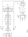
- FIG. 7 is a circuit diagram showing circuitry for adjusting the gain in a class D modulator, according to various embodiments of the disclosure.
- FIG. 8 shows a graph of a Fast Fourier Transform, according to various embodiments of the disclosure.
- FIG. 9 is a flow chart illustrating a method for a playback path, according to various embodiments.
- FIG. 10 is a block diagram of an example electrical device that may include one or more class D modulators, in accordance with various embodiments of the disclosure.
- Systems and methods are provided for circuit configurations that maintain audio playback performance while reducing power consumption.
- a gain for a current digital-to-analog converter in an audio playback path is adjusted based on an amplitude of the input signal.
- systems and methods are provided for transitioning between a modes of operation for large signals and mode of operation for small signals.
- FIG. 1 depicts an audio playback path 100 including headphone or speaker drivers.
- the audio playback path 100 includes a serial port and interpolator 102 , a modulator 104 , and a noise-shaping splitter 106 .
- An input signal is input to the serial port and interpolator 102 .
- the input signal includes multiple samples and bus widths.
- the input signal includes 24 bit input.
- the input signal is interpolated and input to the modulator 104 .
- the interpolation filter uses canonical signed digit arithmetic, and thus has low power consumption.
- the modulator 104 is a second order modulator.
- the modulator 104 is an eight bit modulator.
- the modulator output is input to the noise-shaping splitter 106 .
- the noise shaping splitter 106 splits the signal into three parallel processing lines, and outputs a first sample set to a first line 150 a , a second sample set to a second line 150 b , and a third sample set to a third line 150 c.
- Each of the first 150 a , second 150 b , and third 150 c parallel processing lines includes a sign-magnitude conversion element 108 a , 108 b , 108 c , a rotational scrambler 110 a , 110 b , 110 c , an I-DAC driver 112 a , 112 b , 112 c , and an I-DAC 114 a , 114 b , 114 c .
- the I-DACs 114 a , 114 b , 114 c are 2-level I-DACs
- the I-DACs 114 a , 114 b , 114 c are 3-level DACs.
- the signal is a digital signal through to the rotational scrambler (section 140 ), which outputs a digital signal to the I-DAC driver 112 a , 112 b , 112 c .
- the audio playback path 100 depicts a 1st-order noise shaped segmentation technique.
- the sign-magnitude conversion elements 108 a , 108 b , 108 c perform sign magnitude thermometer code conversion.
- the one or more of the scramblers 110 a , 110 b , 110 c apply individual discrete element modeling (DEM) to the signals in one or more of the respective parallel processing lines 150 a , 150 b , 150 c .
- DEM individual discrete element modeling
- the DEM is rotational in nature.
- the DEM is first order DEM, and in some examples, the DEM is higher order DEM such as second order DEM, third order DEM, or higher.
- the outputs from the first 150 a , second 150 b , and third 150 c parallel processing lines are input to ISI free switching element 116 .
- the outputs are also connected to parallel resistors 132 a , 132 b connected to the playback line 100 output.
- the switching element 116 output is input to an operational amplifier 118 .
- the operational amplifier 118 and the resistors 132 a , 132 b dominate the noise contributions following the first 150 a , second 150 b , and third 150 c parallel lines.
- the audio playback path 100 also includes an I-DAC bias generator 120 , a bandgap element 122 , and an ISI free clock generation 124 .
- the playback path 100 includes one or more elements described herein.
- the opamp 118 and resistors 132 a and 132 b constitute a current to voltage converter which translate the overall current (provided by the current cells in the IDACs 214 a , 214 b , 241 c ) to an output voltage.
- FIG. 2 depicts another example playback path architecture 200 , according to various embodiments of the disclosure.
- the audio playback path architecture 200 includes a serial port and interpolator 202 , a modulator 204 , and a noise-shaping splitter 106 .
- the audio playback path architecture 200 also includes a gain processing block 260 .
- the audio playback path architecture 200 increases the current for small signals, thereby improving audio playback performance. According to one implementation, the increase in current for small signals is achieved with the use of a smaller resistor for the current to voltage conversion.
- An input signal is input to the serial port and interpolator 202 .
- the input signal is interpolated and input to the modulator 204 .
- the modulator 204 is a second order modulator.
- the modulator 204 is an eight bit modulator.
- the modulator output is input to the noise-shaping splitter 206 .
- the noise shaping splitter 206 splits the signal into three parallel processing lines, and outputs a first sample set to a first line 250 a , a second sample set to a second line 250 b , and a third sample set to a third line 250 c.
- Each of the first 250 a , second 250 b , and third 250 c parallel processing lines includes a sign-magnitude conversion element 208 a , 208 b , 208 c , a rotational scrambler 210 a , 210 b , 210 c , an I-DAC driver 212 a , 212 b , 212 c , and a 3-level I-DAC 214 a , 214 b , 214 c .
- the signal is a digital signal through to the rotational scrambler (section 240 ), which outputs an analog signal to the I-DAC driver 212 a , 212 b , 212 c .
- the signal is an analog signal in the next section 242 of the first 250 a , second 250 b , and third 250 c parallel processing lines.
- the I-DACs 214 a , 214 b , 214 c can be any type of DAC, including, for example, a current-steering DAC, a resistive DAC (a voltage domain DAC), and a capacitive DAC (cap-DAC).
- the I-DACs 214 a , 214 b , 214 c includes multiple cells, and many of the cells are not in use when incoming signals are small.
- an I-DAC would typically use a first resistance and two cells to process a small signal.
- the current is doubled such that the I-DAC uses four cells, and the resistance is decreased accordingly to maintain an equivalent output voltage.
- the digital amplitude can be changed to change the gain of the I-DAC 214 a , 214 b , 214 c .
- a reference voltage is used to generate the currents, and, in some examples, the reference voltage is changed to decrease the thermal noise of the I-DAC 214 a , 214 b , 214 c (instead of changing the number of cells) and the digital amplitude remains the same.
- the gain processing block 260 performs a look-ahead function to determine the state of the I-DACs 214 a , 214 b , 214 c .
- the gain processing block 260 receives the input signal to the serial port and interpolator 202 , and determines for each of the I-DACs 214 a , 214 b , 214 c whether the I-DAC is in a 1 ⁇ , 2 ⁇ , 4 ⁇ , or 8 ⁇ state, based on the upcoming signals. In one example, when the amplitude of the upcoming signals is small, the gain processing block 260 increases the number of cells used in each I-DAC 214 a , 214 b , 214 c . In some examples, the reference voltage to the IDAC 214 a , 214 b , 214 c is changed to increase or decrease the output current per cell.
- the opamp 218 and resistors 232 a and 232 b constitute a current to voltage converter, which translates the overall current (provided by the current cells in the I-DACs, 214 a , 214 b , 241 c ) to an output voltage.
- the gain processing block 260 is also coupled to the parallel resistors 232 a , 232 b at the output of the parallel processing lines 250 a , 250 b , 250 c .
- the gain processing block 260 also changes the resistance of the parallel resistors 232 a , 232 b based on the size of upcoming signals. For smaller signals, the resistance of the parallel resistors 232 a , 232 b is decreased, while for larger signals, the resistance of the parallel resistors 232 a , 232 b is increased.
- the gain processing block 260 increases the current by 2 ⁇ by increasing the number of cells used in an I-DAC 214 a , 214 b , 214 c by two, and reducing the I-V resistance by 2 ⁇ . These changes can also be done for other gains in the circuit.
- the gain processing block 260 changes the number of cells used in an I-DAC 214 a , 214 b , 214 c by changing the digital amplitude.
- the gain processing block 260 has a look-ahead feature, as described above, and the signal in the audio playback path is delayed, for example at the modulator 204 .
- the gain processing block 260 increases the current by 2 ⁇ by increasing the reference voltage to each I-DAC 214 a , 214 b , 214 c .
- the number of cells used in each I-DAC 214 a , 214 b , 214 c remains the unchanged and the current is changed by adjusting the reference voltage. Additionally, in this example, the output amplitude remains unchanged.
- the gain processing block 260 adjusts the gain at various points in the playback path architecture 200 .
- the gain processing block 260 adjusts digital gain (e.g., by determining the number of cells that are active in an I-DAC 214 a , 214 b , 214 c , or by changing the reference voltage to an I-DAC 214 a , 214 b , 214 c to adjust the individual current value).
- the analog gain is then adjusted to correspond to the digital gain, based on the current-voltage resistance value. Additionally, in this example, the output amplitude remains unchanged.
- FIG. 3 shows a diagram for an automatic gain control (AGC) circuit 300 , according to various embodiments of the disclosure.
- the gain control circuit 300 of FIG. 3 includes an input 302 , a first amplifier 304 , input resistors 308 , and a second amplifier 306 .
- a digital automatic gain control is canceled by an analog automatic gain control.
- the first amplifier 304 is an operational amplifier in a playback path such as amplifier 218 in the playback path circuit 200
- the amplifier 306 is added after the operational amplifier in a playback path circuit 200 .
- the second amplifier 306 is performs analog gain control.
- the resistance for the second amplifier 306 is fixed, and different gains are achieved by switching the internal tap point for the amplifier 306 input terminals. This allows the gain setting to be changed while maintaining the overall resistance for all gain settings. Thus, in this example, the overall resistance remains the same independent of the gain settings.
- the feedback resistance (R 0 ) and input resistance (R 1 ) are changed for various gain settings, but the value of the total feedback resistance (R 0 +R 1 ) is fixed.
- the gains on the second amplifier 306 are changed to improve the signal to noise ratio for small signals.
- automatic gain control is used for scaling a signal-to-noise ratio.
- small output i.e., small signal
- amplifier noise gain can become small, and DAC noise can be attenuated.
- small signal amplifier noise gain is 1 ⁇ 4, and DAC SNR is improved by approximately 12 dB.
- amplifier noise gain may be considered to be 4 decibels (dB) better.
- FIG. 4 shows a diagram for an automatic gain control (AGC) circuit 400 , according to various embodiments of the disclosure.
- the gain control circuit 400 of FIG. 4 includes an input 402 , a first amplifier 404 , a second amplifier 406 , and an array of parallel resistors 408 .
- the first amplifier 404 is an operational amplifier in a playback path such as the amplifier 218 in the playback path circuit 200
- the array of parallel resistors 408 and the amplifier 406 are added after the operational amplifier in a playback path circuit 200 .
- the array of parallel resistors 408 are followed by switches, which allow for the use of one or more of the resistors 408 at a time.
- the switches can be used to select resistors and allow for changes in the total input resistance (R 1 ), based on the resistor selection.
- the switches are programmable switches.
- the second amplifier 406 performs analog gain control.
- gain mismatch can be shaped. The gain is changed by switching in parallel resistances to change the equivalent input resistance (R 1 ), while the feedback resistance (R 0 ) remains the same for all gain settings.
- FIG. 5 shows four graphs of signal levels over time during a playback operation, according to various embodiments of the disclosure.
- the signal levels begin with a small input signal, and, as shown in the first graph 502 , gain is high in the DAC for a small input signal. In particular, digital gain in the DAC is high, while analog gain is low.
- the second graph 504 shows the desired output.
- the third graph 506 shows the digital output with the desired gain settings.
- the fourth graph 508 shows the analog output from the system. Note that the analog output shown in the fourth graph 508 is very close to the desired output shown in the second graph 504 .
- the input signal increases, and the digital gain is reduced, while the analog gain is increased. Note that by increasing the analog gain when the digital gain is reduced, the overall gain of the system remains constant. As shown in the graphs for desired output 504 , digital output 506 , and analog output 508 , at the limit mark 510 , the output signals also increase. In some examples, the transition at the limit mark has a small gain step. In one example, the gain step is on the order of 0.375 dB digital/analog gain step. When the input signal decreases again to a small input signal, the system holds for a period 512 before increasing the digital gain and reducing the analog gain again at the release mark 514 .
- a recovery operation is performed to increase the digital gain and reduce the analog gain.
- the recovery operation is performed at a zero-crossing.
- the “hold” period helps prevent frequent changes in gain due to short changes in the signal.
- FIGS. 6A and 6B show example circuitry 600 for an input stage of a class-D modulator or an ADC, and the input stage to add signals actively using an operational amplifier, respectively, according to various embodiments of the disclosure.
- the circuitry 600 is used in an integrator.
- the circuit 600 includes an I-DAC 602 .
- the current feedback signal is output from a class D output stage. When the current in the I-DAC changes, this is countered in the amplifier circuitry 604 on the right.
- the I-DAC 602 current is reduced by 2/3 and the feedback resistance in the amplifier circuitry 604 is increased by 3/2.
- an alternate path for the current through the amplifier circuitry 604 takes some of the feedback current, increasing the gain of the I-DAC 602 .
- the circuitry 600 shown in FIG. 6A shunts away the current to increase the effective resistance.
- a shunt gate control can be used to change the feedback gain from 1 to 3/2.
- one of a series resistance and a shunt resistance is changed.
- the feedback is changed from 10 k to 15 k by changing the series resistance.
- FIG. 7 is a circuit diagram showing circuitry 700 for adjusting the gain in a class D modulator, according to various embodiments of the disclosure. As shown in FIG. 7 , a feedback loop is included such that when resistance at a DAC 702 is decreased, the resistance at the resistors 710 a , 710 b is increased.
- the circuit 700 includes a DAC 702 , a loop filter 708 , a capacitance module 712 , a quantizer 714 , a control block 716 , and a power stage 718 .
- the DAC 702 is a current mode DAC.
- the output from the power stage 718 is fed back to the loop filter input, and the feedback lines include variable resistors 710 a , 710 b .
- the resistance on each of the variable resistors 710 a , 710 b can be varied to alter the current input.
- the loop filter 708 output is input to the capacitance module 712 at input 720 . Additionally, reference voltages refn and refp are input to the capacitance module 712 .
- the output from the power stage 718 is the circuit 700 output.
- the circuitry 604 from FIG. 6A and the circuitry 620 from FIG. 6B can be combined with the circuitry 700 .
- Resistance at the resistors 710 a , 710 b is changed based on changes in resistance at the I-DAC 702 . For example, when resistance at the I-DAC 702 is decreased, the resistance at the resistors 710 a - 710 b is increased. In one example, the current at the I-DAC 702 is reduced by 2/3 and the resistance at the resistors 710 a , 710 b is increased to 3/2. Additionally, the references refp and refn to the quantizer 714 are reduced to maintain the overall state of the output signal from the circuit 700 .
- the capacitance module 712 includes capacitors with variable capacitance, which can be used to adjust the references refp and refn to the quantizer 714 .
- FIG. 8 shows a graph 800 of a Fast Fourier Transform, according to various embodiments of the disclosure.
- the graph 800 shows a FFT of the modulator performance in power saving mode.
- an FFT of modulator performance in high performance mode yields similar results.
- FIG. 9 is a flow chart illustrating a method 900 for a playback path, according to various embodiments.
- an input signal is received at a playback path input.
- the input signal is also received at a gain processing module, and, at step 904 , the gain processing module determines a gain for an I-DAC based on an amplitude of the input signal.
- the gain processing module detects a change in the amplitude of the input signal, and adjusts the gain of the I-DAC based on the amplitude change. If the amplitude of the input signal increases, the gain processing module decreases the gain of the I-DAC. If the amplitude of the input signal decreases, the gain processing module increases the gain of the I-DAC. However, before increasing the gain of the I-DAC, the gain processing module maintains the gain for a selected period of time. The hold period prevents frequent changes in gain.
- the gain for the I-DAC is a digital gain.
- a second gain is adjusted based on the change in gain for the I-DAC.
- the gain of an amplifier downstream from the I-DAC is adjusted.
- the amplifier can be an inverted amplifier.
- the second gain is adjusted such that the total gain of the output signal remains the same despite the change in gain at the I-DAC.
- the second gain is an analog gain.
- the input signal is processed through a series of circuitry elements as shown in FIGS. 1 and 2 .
- FIG. 10 is a block diagram of an example electrical device 1000 that may include one or more digital class D drivers, in accordance with any of the embodiments disclosed herein.
- a number of components are illustrated in FIG. 10 as included in the electrical device 1000 , but any one or more of these components may be omitted or duplicated, as suitable for the application.
- some or all of the components included in the electrical device 1000 may be attached to one or more motherboards.
- some or all of these components are fabricated onto a single system-on-a-chip (SoC) die.
- SoC system-on-a-chip
- the electrical device 1000 may not include one or more of the components illustrated in FIG. 10 , but the electrical device 1000 may include interface circuitry for coupling to the one or more components.
- the electrical device 1000 may not include a display device 1006 , but may include display device interface circuitry (e.g., a connector and driver circuitry) to which a display device 1006 may be coupled.
- the electrical device 1000 may not include an audio input device 1024 or an audio output device 1008 , but may include audio input or output device interface circuitry (e.g., connectors and supporting circuitry) to which an audio input device 1024 or audio output device 1008 may be coupled.
- the electrical device 1000 may include a processing device 1002 (e.g., one or more processing devices).
- processing device e.g., one or more processing devices.
- the term “processing device” or “processor” may refer to any device or portion of a device that processes electronic data from registers and/or memory to transform that electronic data into other electronic data that may be stored in registers and/or memory.
- the processing device 1002 may include one or more digital signal processors (DSPs), application-specific integrated circuits (ASICs), central processing units (CPUs), graphics processing units (GPUs), cryptoprocessors (specialized processors that execute cryptographic algorithms within hardware), server processors, or any other suitable processing devices.
- DSPs digital signal processors
- ASICs application-specific integrated circuits
- CPUs central processing units
- GPUs graphics processing units
- cryptoprocessors specialized processors that execute cryptographic algorithms within hardware
- server processors or any other suitable processing devices.
- the electrical device 1000 may include a memory 1004 , which may itself include one or more memory devices such as volatile memory (e.g., dynamic random access memory (DRAM)), nonvolatile memory (e.g., read-only memory (ROM)), flash memory, solid state memory, and/or a hard drive.
- volatile memory e.g., dynamic random access memory (DRAM)
- nonvolatile memory e.g., read-only memory (ROM)
- flash memory solid state memory
- solid state memory solid state memory
- hard drive e.g., solid state memory, and/or a hard drive.
- the memory 1004 may include memory that shares a die with the processing device 1002 . This memory may be used as cache memory and may include embedded dynamic random access memory (eDRAM) or spin transfer torque magnetic random access memory (STT-MRAM).
- eDRAM embedded dynamic random access memory
- STT-MRAM spin transfer torque magnetic random access memory
- the electrical device 1000 may include a communication chip 1012 (e.g., one or more communication chips).
- the communication chip 1012 may be configured for managing wireless communications for the transfer of data to and from the electrical device 1000 .
- the term “wireless” and its derivatives may be used to describe circuits, devices, systems, methods, techniques, communications channels, etc., that may communicate data through the use of modulated electromagnetic radiation through a nonsolid medium. The term does not imply that the associated devices do not contain any wires, although in some embodiments they might not.
- the communication chip 1012 may implement any of a number of wireless standards or protocols, including but not limited to Institute for Electrical and Electronic Engineers (IEEE) standards including Wi-Fi (IEEE 802.11 family), IEEE 802.16 standards (e.g., IEEE 802.16-2005 Amendment), Long-Term Evolution (LTE) project along with any amendments, updates, and/or revisions (e.g., advanced LTE project, ultra mobile broadband (UMB) project (also referred to as “3GPP2”), etc.).
- IEEE 802.16 compatible Broadband Wireless Access (BWA) networks are generally referred to as WiMAX networks, an acronym that stands for Worldwide Interoperability for Microwave Access, which is a certification mark for products that pass conformity and interoperability tests for the IEEE 802.16 standards.
- the communication chip 1012 may operate in accordance with a Global System for Mobile Communication (GSM), General Packet Radio Service (GPRS), Universal Mobile Telecommunications System (UMTS), High Speed Packet Access (HSPA), Evolved HSPA (E-HSPA), or LTE network.
- GSM Global System for Mobile Communication
- GPRS General Packet Radio Service
- UMTS Universal Mobile Telecommunications System
- High Speed Packet Access HSPA
- E-HSPA Evolved HSPA
- LTE LTE network.
- the communication chip 1012 may operate in accordance with Enhanced Data for GSM Evolution (EDGE), GSM EDGE Radio Access Network (GERAN), Universal Terrestrial Radio Access Network (UTRAN), or Evolved UTRAN (E-UTRAN).
- EDGE Enhanced Data for GSM Evolution
- GERAN GSM EDGE Radio Access Network
- UTRAN Universal Terrestrial Radio Access Network
- E-UTRAN Evolved UTRAN
- the communication chip 1012 may operate in accordance with Code Division Multiple Access (CDMA), Time Division Multiple Access (TDMA), Digital Enhanced Cordless Telecommunications (DECT), Evolution-Data Optimized (EV-DO), and derivatives thereof, as well as any other wireless protocols that are designated as 3G, 4G, 5G, and beyond.
- CDMA Code Division Multiple Access
- TDMA Time Division Multiple Access
- DECT Digital Enhanced Cordless Telecommunications
- EV-DO Evolution-Data Optimized
- the communication chip 1012 may operate in accordance with other wireless protocols in other embodiments.
- the electrical device 1000 may include an antenna 1022 to facilitate wireless communications and/or to receive other wireless communications (such as AM or FM radio transmissions).
- the communication chip 1012 may manage wired communications, such as electrical, optical, or any other suitable communication protocols (e.g., the Ethernet).
- the communication chip 1012 may include multiple communication chips. For instance, a first communication chip 1012 may be dedicated to shorter-range wireless communications such as Wi-Fi or Bluetooth, and a second communication chip 1012 may be dedicated to longer-range wireless communications such as global positioning system (GPS), EDGE, GPRS, CDMA, WiMAX, LTE, EV-DO, or others.
- GPS global positioning system
- EDGE EDGE
- GPRS global positioning system
- CDMA Code Division Multiple Access
- WiMAX Code Division Multiple Access
- LTE Long Term Evolution
- EV-DO Evolution-DO
- the electrical device 1000 may include battery/power circuitry 1014 .
- the battery/power circuitry 1014 may include one or more energy storage devices (e.g., batteries or capacitors) and/or circuitry for coupling components of the electrical device 1000 to an energy source separate from the electrical device 1000 (e.g., AC line power).
- the electrical device 1000 may include a display device 1006 (or corresponding interface circuitry, as discussed above).
- the display device 1006 may include any visual indicators, such as a heads-up display, a computer monitor, a projector, a touchscreen display, a liquid crystal display (LCD), a light-emitting diode display, or a flat panel display.
- the electrical device 1000 may include an audio output device 1008 (or corresponding interface circuitry, as discussed above).
- the audio output device 1008 may include any device that generates an audible indicator, such as speakers, headsets, or earbuds.
- the electrical device 1000 may include an audio input device 1024 (or corresponding interface circuitry, as discussed above).
- the audio input device 1024 may include any device that generates a signal representative of a sound, such as microphones, microphone arrays, or digital instruments (e.g., instruments having a musical instrument digital interface (MIDI) output).
- MIDI musical instrument digital interface
- the electrical device 1000 may include a GPS device 1018 (or corresponding interface circuitry, as discussed above).
- the GPS device 1018 may be in communication with a satellite-based system and may receive a location of the electrical device 1000 , as known in the art.
- the electrical device 1000 may include another output device 1010 (or corresponding interface circuitry, as discussed above).
- Examples of the other output device 1010 may include an audio codec, a video codec, a printer, a wired or wireless transmitter for providing information to other devices, or an additional storage device.
- the electrical device 1000 may include another input device 1020 (or corresponding interface circuitry, as discussed above).
- Examples of the other input device 1020 may include an accelerometer, a gyroscope, a compass, an image capture device, a keyboard, a cursor control device such as a mouse, a stylus, a touchpad, a bar code reader, a Quick Response (QR) code reader, any sensor, or a radio frequency identification (RFID) reader.
- the electrical device 1000 may have any desired form factor, such as a handheld or mobile electrical device (e.g., a cell phone, a smart phone, a mobile internet device, a music player, a tablet computer, a laptop computer, a netbook computer, an ultrabook computer, a personal digital assistant (PDA), an ultra mobile personal computer, etc.), a desktop electrical device, a server device or other networked computing component, a printer, a scanner, a monitor, a set-top box, an entertainment control unit, a vehicle control unit, a digital camera, a digital video recorder, or a wearable electrical device.
- the electrical device 1000 may be any other electronic device that processes data.
- Example 1 provides an audio playback circuit, comprising a plurality of current digital-to-analog converters (I-DACs) configured to receive a processed input signal, a plurality of resistors coupled to an output from the plurality of DACs, and a gain processing module configured to determine, based on an input signal, a gain for each of the plurality of DACs and a resistance of each of the plurality of resistors, wherein the input signal is processed to generate the processed input signal
- I-DACs current digital-to-analog converters
- Example 2 provides the circuit according to one or more of the preceding and/or following examples, wherein the gain processing module is configured to detect a change in amplitude of the input signal, and wherein the gain processing module is configured to decrease the gain for each of the plurality of I-DACs when an input signal amplitude is large and to increase the gain for each of the plurality of I-DACs when an input signal amplitude is small.
- Example 3 provides a circuit according to one or more of the preceding and/or following examples, wherein when a decrease in amplitude is detected, the gain processing module is configured to maintain the gain for each of the plurality of I-DACs for a selected period of time.
- Example 4 provides a circuit according to one or more of the preceding and/or following examples, wherein the gain processing module is configured to decrease the resistance of each of the plurality of resistors when the input signal amplitude is small.
- Example 5 provides a circuit according to one or more of the preceding and/or following examples, wherein each of the plurality of I-DACs includes a plurality of cells, and wherein the gain processing module increases a number of the plurality of cells that are active in each of the plurality of I-DACs to increase the gain of the plurality of I-DACs.
- Example 7 provides a circuit according to one or more of the preceding and/or following examples, wherein the gain processing module is configured to adjust a reference voltage to each of the plurality of DACs to adjust the current
- Example 8 provides a circuit according to one or more of the preceding and/or following examples, further comprising a feedback loop between the plurality of resistors and the plurality of I-DACs.
- Example 9 provides a circuit according to one or more of the preceding and/or following examples, further comprising a quantizer coupled to a playback circuit output, wherein the quantizer has a quantizer gain, and the quantizer gain is related to the gain for each of the plurality of I-DACs.
- Example 10 provides a circuit according to one or more of the preceding and/or following examples, wherein the gain processing module is further configured to use automatic gain control to adjust the gain for each of the plurality of I-DACs.
- Example 11 provides a modulator having an adjustable gain, including a digital-to-analog converter (DAC) configured to receive an input signal and generate an analog signal; a set of resistors coupled to an output from the DAC, wherein each of the set of resistors has a variable resistance, and the resistance of each of the resistors is correlated with the output of the DAC; a loop filter configured to filter the analog signal and output a loop filter output; a summer configured to generate a summed signal based on the loop filter output and a reference voltage, wherein the summer includes a variable capacitor; a quantizer configured to quantize the summed signal; and a power stage configured to generate a modulator output.
- DAC digital-to-analog converter
- Example 12 provides a modulator according to one or more of the preceding and/or following examples, further comprising a set of feedback lines from the modulator output to the loop filter, wherein the set of feedback lines is coupled to the output from the DAC, wherein each of the set of feedback lines includes a respective resistor from the set of resistors.
- Example 13 provides a modulator according to one or more of the preceding and/or following examples, wherein, for a first input signal, each resistor of the set of resistors, the reference voltage, and the outputs from the DAC have different values.
- Example 14 provides a modulator according to one or more of the preceding and/or following examples, wherein, for the first input signal, the different values are configured to be on different clock cycles.
- Example 15 provides a modulator according to one or more of the preceding and/or following examples wherein the DAC is one of a current mode DAC, a voltage mode DAC, and a charge mode DAC.
- Example 16 provides a modulator according to one or more of the preceding and/or following examples, further comprising a current shunt coupled to at least one of the DAC and the resistors, wherein the current shunt is configured to shunt the current causing the resistance of each of the resistors to increase.
- Example 17 provides a method for processing signals in an audio playback path, comprising receiving an input signal at a playback path input; determining, at a gain processing module, a digital gain for a digital-to-analog converter (DAC) based on an amplitude of the input signal; and adjusting an analog gain for an amplifier based on the digital gain.
- DAC digital-to-analog converter
- Example 18 provides a method according to one or more of the preceding and/or following examples, further comprising detecting a change in the amplitude of the input signal.
- Example 19 provides a method according to one or more of the preceding and/or following examples, further comprising decreasing the gain of the DAC when an increase in the amplitude of the input signal is detected; and increasing the gain of the DAC when a decrease in the amplitude of the input signal is detected.
- Example 20 provides a method according to one or more of the preceding and/or following examples, further comprising maintaining the gain of the DAC for a selected period of time when the decrease in the amplitude of the input signal is detected.
- Example 21 includes an apparatus that includes a playback circuit as discussed or depicted in any of the preceding examples, some other example, or as otherwise discussed or depicted herein.
- Example 22 includes an apparatus comprising means to implement a playback circuit as discussed or depicted in any of the preceding examples, some other example, or as otherwise discussed or depicted herein.
- Example 23 includes a method for implementing or manufacturing a playback circuit as discussed or depicted in any of the preceding examples, some other example, or as otherwise discussed or depicted herein.
- Example 24 includes one or more non-transitory computer-readable media comprising instructions that, upon execution of the instructions by an electronic device, are to cause the electronic device to implement or manufacture a playback circuit as discussed or depicted in any of the preceding examples, some other example, or as otherwise discussed or depicted herein.
- the PHOSITA will appreciate that they may readily use the present disclosure as a basis for designing or modifying other processes, structures, or variations for carrying out the same purposes and/or achieving the same advantages of the embodiments introduced herein.
- the PHOSITA will also recognize that such equivalent constructions do not depart from the spirit and scope of the present disclosure, and that they may make various changes, substitutions, and alterations herein without departing from the spirit and scope of the present disclosure.
- One or more aspects and embodiments of the present application involving the performance of processes or methods may utilize program instructions executable by a device (e.g., a computer, a processor, or other device) to perform, or control performance of, the processes or methods.
- a device e.g., a computer, a processor, or other device
- inventive concepts may be embodied as a computer readable storage medium (or multiple computer readable storage media) (e.g., a computer memory, one or more floppy discs, compact discs, optical discs, magnetic tapes, flash memories, circuit configurations in Field Programmable Gate Arrays or other semiconductor devices, or other tangible computer storage medium) encoded with one or more programs that, when executed on one or more computers or other processors, perform methods that implement one or more of the various embodiments described above.
- a computer readable storage medium e.g., a computer memory, one or more floppy discs, compact discs, optical discs, magnetic tapes, flash memories, circuit configurations in Field Programmable Gate Arrays or other semiconductor devices, or other tangible computer storage medium
- the computer readable medium or media may be transportable, such that the program or programs stored thereon may be loaded onto one or more different computers or other processors to implement various ones of the aspects described above.
- computer readable media may be non-transitory media.
- teachings of the present disclosure may be encoded into one or more tangible, non-transitory computer-readable mediums having stored thereon executable instructions that, when executed, instruct a programmable device (such as a processor or DSP) to perform the methods or functions disclosed herein.
- a programmable device such as a processor or DSP
- a non-transitory medium could include a hardware device hardware-programmed with logic to perform the methods or functions disclosed herein.
- the teachings could also be practiced in the form of Register Transfer Level (RTL) or other hardware description language such as VHDL or Verilog, which can be used to program a fabrication process to produce the hardware elements disclosed.
- RTL Register Transfer Level
- VHDL Verilog
- processing activities outlined herein may also be implemented in software.
- one or more of these features may be implemented in hardware provided external to the elements of the disclosed figures, or consolidated in any appropriate manner to achieve the intended functionality.
- the various components may include software (or reciprocating software) that can coordinate in order to achieve the operations as outlined herein.
- these elements may include any suitable algorithms, hardware, software, components, modules, interfaces, or objects that facilitate the operations thereof.
- Any suitably-configured processor component can execute any type of instructions associated with the data to achieve the operations detailed herein.
- Any processor disclosed herein could transform an element or an article (for example, data) from one state or thing to another state or thing.
- some activities outlined herein may be implemented with fixed logic or programmable logic (for example, software and/or computer instructions executed by a processor) and the elements identified herein could be some type of a programmable processor, programmable digital logic (for example, an FPGA, an erasable programmable read only memory (EPROM), an electrically erasable programmable read only memory (EEPROM)), an ASIC that includes digital logic, software, code, electronic instructions, flash memory, optical disks, CD-ROMs, DVD ROMs, magnetic or optical cards, other types of machine-readable mediums suitable for storing electronic instructions, or any suitable combination thereof.
- EPROM erasable programmable read only memory
- EEPROM electrically erasable programmable read only memory
- processors may store information in any suitable type of non-transitory storage medium (for example, random access memory (RAM), read only memory (ROM), FPGA, EPROM, electrically erasable programmable ROM (EEPROM), etc.), software, hardware, or in any other suitable component, device, element, or object where appropriate and based on particular needs.
- RAM random access memory
- ROM read only memory
- FPGA field-programmable gate array
- EPROM electrically erasable programmable ROM
- EEPROM electrically erasable programmable ROM
- any of the memory items discussed herein should be construed as being encompassed within the broad term ‘memory.’
- any of the potential processing elements, modules, and machines described herein should be construed as being encompassed within the broad term ‘microprocessor’ or ‘processor.’
- the processors, memories, network cards, buses, storage devices, related peripherals, and other hardware elements described herein may be realized by a processor, memory, and other related devices configured by software or firmware to emulate or virtualize the functions of those hardware elements.
- a computer may be embodied in any of a number of forms, such as a rack-mounted computer, a desktop computer, a laptop computer, or a tablet computer, as non-limiting examples. Additionally, a computer may be embedded in a device not generally regarded as a computer but with suitable processing capabilities, including a personal digital assistant (PDA), a smart phone, a mobile phone, an iPad, or any other suitable portable or fixed electronic device.
- PDA personal digital assistant
- a computer may have one or more input and output devices. These devices can be used, among other things, to present a user interface. Examples of output devices that may be used to provide a user interface include printers or display screens for visual presentation of output and speakers or other sound generating devices for audible presentation of output. Examples of input devices that may be used for a user interface include keyboards, and pointing devices, such as mice, touch pads, and digitizing tablets. As another example, a computer may receive input information through speech recognition or in other audible formats.
- Such computers may be interconnected by one or more networks in any suitable form, including a local area network or a wide area network, such as an enterprise network, and intelligent network (IN) or the Internet.
- networks may be based on any suitable technology and may operate according to any suitable protocol and may include wireless networks or wired networks.
- Computer-executable instructions may be in many forms, such as program modules, executed by one or more computers or other devices.
- program modules include routines, programs, objects, components, data structures, etc. that performs particular tasks or implement particular abstract data types.
- functionality of the program modules may be combined or distributed as desired in various embodiments.
- program or “software” are used herein in a generic sense to refer to any type of computer code or set of computer-executable instructions that may be employed to program a computer or other processor to implement various aspects as described above. Additionally, it should be appreciated that according to one aspect, one or more computer programs that when executed perform methods of the present application need not reside on a single computer or processor, but may be distributed in a modular fashion among a number of different computers or processors to implement various aspects of the present application.
- data structures may be stored in computer-readable media in any suitable form.
- data structures may be shown to have fields that are related through location in the data structure. Such relationships may likewise be achieved by assigning storage for the fields with locations in a computer-readable medium that convey relationship between the fields.
- any suitable mechanism may be used to establish a relationship between information in fields of a data structure, including through the use of pointers, tags or other mechanisms that establish relationship between data elements.
- the software code When implemented in software, the software code may be executed on any suitable processor or collection of processors, whether provided in a single computer or distributed among multiple computers.
- Computer program logic implementing all or part of the functionality described herein is embodied in various forms, including, but in no way limited to, a source code form, a computer executable form, a hardware description form, and various intermediate forms (for example, mask works, or forms generated by an assembler, compiler, linker, or locator).
- source code includes a series of computer program instructions implemented in various programming languages, such as an object code, an assembly language, or a high-level language such as OpenCL, RTL, Verilog, VHDL, Fortran, C, C++, JAVA, or HTML for use with various operating systems or operating environments.
- the source code may define and use various data structures and communication messages.
- the source code may be in a computer executable form (e.g., via an interpreter), or the source code may be converted (e.g., via a translator, assembler, or compiler) into a computer executable form.
- any number of electrical circuits of the FIGURES may be implemented on a board of an associated electronic device.
- the board can be a general circuit board that can hold various components of the internal electronic system of the electronic device and, further, provide connectors for other peripherals. More specifically, the board can provide the electrical connections by which the other components of the system can communicate electrically.
- Any suitable processors (inclusive of digital signal processors, microprocessors, supporting chipsets, etc.), memory elements, etc. can be suitably coupled to the board based on particular configuration needs, processing demands, computer designs, etc.
- FIGURES may be implemented as standalone modules (e.g., a device with associated components and circuitry configured to perform a specific application or function) or implemented as plug-in modules into application-specific hardware of electronic devices.
- some aspects may be embodied as one or more methods.
- the acts performed as part of the method may be ordered in any suitable way. Accordingly, embodiments may be constructed in which acts are performed in an order different than illustrated, which may include performing some acts simultaneously, even though shown as sequential acts in illustrative embodiments.
- connection means any connection or coupling, either direct or indirect, between two or more elements; the coupling or connection between the elements can be physical, logical, or a combination thereof.
- references to “A and/or B”, when used in conjunction with open-ended language such as “comprising” may refer, in one embodiment, to A only (optionally including elements other than B); in another embodiment, to B only (optionally including elements other than A); in yet another embodiment, to both A and B (optionally including other elements); etc.
- the phrase “at least one,” in reference to a list of one or more elements, should be understood to mean at least one element selected from any one or more of the elements in the list of elements, but not necessarily including at least one of each and every element specifically listed within the list of elements and not excluding any combinations of elements in the list of elements.
- This definition also allows that elements may optionally be present other than the elements specifically identified within the list of elements to which the phrase “at least one” refers, whether related or unrelated to those elements specifically identified.
- “at least one of A and B” may refer, in one embodiment, to at least one, optionally including more than one, A, with no B present (and optionally including elements other than B); in another embodiment, to at least one, optionally including more than one, B, with no A present (and optionally including elements other than A); in yet another embodiment, to at least one, optionally including more than one, A, and at least one, optionally including more than one, B (and optionally including other elements); etc.
- the term “between” is to be inclusive unless indicated otherwise.
- “between A and B” includes A and B unless indicated otherwise.
Landscapes
- Engineering & Computer Science (AREA)
- Multimedia (AREA)
- Theoretical Computer Science (AREA)
- Health & Medical Sciences (AREA)
- Audiology, Speech & Language Pathology (AREA)
- General Health & Medical Sciences (AREA)
- Human Computer Interaction (AREA)
- Physics & Mathematics (AREA)
- General Engineering & Computer Science (AREA)
- General Physics & Mathematics (AREA)
- Control Of Amplification And Gain Control (AREA)
- Amplifiers (AREA)
Abstract
Description
Claims (20)
Priority Applications (1)
| Application Number | Priority Date | Filing Date | Title |
|---|---|---|---|
| US17/030,681 US11411543B2 (en) | 2019-09-24 | 2020-09-24 | Power efficiency in an audio playback path |
Applications Claiming Priority (2)
| Application Number | Priority Date | Filing Date | Title |
|---|---|---|---|
| US201962905324P | 2019-09-24 | 2019-09-24 | |
| US17/030,681 US11411543B2 (en) | 2019-09-24 | 2020-09-24 | Power efficiency in an audio playback path |
Publications (2)
| Publication Number | Publication Date |
|---|---|
| US20210091739A1 US20210091739A1 (en) | 2021-03-25 |
| US11411543B2 true US11411543B2 (en) | 2022-08-09 |
Family
ID=74882312
Family Applications (1)
| Application Number | Title | Priority Date | Filing Date |
|---|---|---|---|
| US17/030,681 Active US11411543B2 (en) | 2019-09-24 | 2020-09-24 | Power efficiency in an audio playback path |
Country Status (1)
| Country | Link |
|---|---|
| US (1) | US11411543B2 (en) |
Families Citing this family (3)
| Publication number | Priority date | Publication date | Assignee | Title |
|---|---|---|---|---|
| US11533033B2 (en) * | 2020-06-12 | 2022-12-20 | Bose Corporation | Audio signal amplifier gain control |
| US12248728B2 (en) * | 2022-06-22 | 2025-03-11 | Stmicroelectronics S.R.L. | Centralized digital mute and volume control |
| US12580540B2 (en) * | 2023-03-31 | 2026-03-17 | Texas Instruments Incorporated | Gain control of audio data using hardware accelerators |
Citations (12)
| Publication number | Priority date | Publication date | Assignee | Title |
|---|---|---|---|---|
| US20130226593A1 (en) * | 2010-11-12 | 2013-08-29 | Nokia Corporation | Audio processing apparatus |
| US8649529B2 (en) * | 2008-06-20 | 2014-02-11 | Fraunhofer-Gesellschaft Zur Foerderung Der Angewandten Forschung E.V. | Apparatus, method and computer program for localizing a sound source |
| US8890608B2 (en) | 2012-02-29 | 2014-11-18 | Texas Instruments Incorporated | Digital input class-D audio amplifier |
| US20150008962A1 (en) * | 2013-07-05 | 2015-01-08 | Wolfson Microelectronics Plc | Signal envelope processing |
| US20170243598A1 (en) * | 2016-02-19 | 2017-08-24 | Imagination Technologies Limited | Controlling Analogue Gain Using Digital Gain Estimation |
| US20170374459A1 (en) * | 2016-06-28 | 2017-12-28 | Cirrus Logic International Semiconductor Ltd. | Optimization of performance and power in audio system |
| US20180351515A1 (en) * | 2017-06-02 | 2018-12-06 | Cirrus Logic International Semiconductor Ltd. | Audio amplifiers |
| US20180352328A1 (en) * | 2017-06-06 | 2018-12-06 | Cirrus Logic International Semiconductor Ltd. | Systems, apparatus and methods for dynamic range enhancement of audio signals |
| US20190007011A1 (en) | 2017-06-30 | 2019-01-03 | Nxp B.V. | Amplifier circuit |
| US20200036352A1 (en) * | 2018-07-25 | 2020-01-30 | Cirrus Logic International Semiconductor Ltd. | Gain control in a class-d open-loop amplifier |
| US20200044628A1 (en) * | 2018-08-06 | 2020-02-06 | Cirrus Logic International Semiconductor Ltd. | Variable output resistance in a playback path with closed-loop pulse-width modulation driver |
| US11070183B1 (en) * | 2020-03-31 | 2021-07-20 | Cirrus Logic, Inc. | Systems, apparatus and methods for dynamic range enhancement of audio signals |
-
2020
- 2020-09-24 US US17/030,681 patent/US11411543B2/en active Active
Patent Citations (13)
| Publication number | Priority date | Publication date | Assignee | Title |
|---|---|---|---|---|
| US8649529B2 (en) * | 2008-06-20 | 2014-02-11 | Fraunhofer-Gesellschaft Zur Foerderung Der Angewandten Forschung E.V. | Apparatus, method and computer program for localizing a sound source |
| US20130226593A1 (en) * | 2010-11-12 | 2013-08-29 | Nokia Corporation | Audio processing apparatus |
| US8890608B2 (en) | 2012-02-29 | 2014-11-18 | Texas Instruments Incorporated | Digital input class-D audio amplifier |
| US20150008962A1 (en) * | 2013-07-05 | 2015-01-08 | Wolfson Microelectronics Plc | Signal envelope processing |
| US20170243598A1 (en) * | 2016-02-19 | 2017-08-24 | Imagination Technologies Limited | Controlling Analogue Gain Using Digital Gain Estimation |
| US20170374459A1 (en) * | 2016-06-28 | 2017-12-28 | Cirrus Logic International Semiconductor Ltd. | Optimization of performance and power in audio system |
| US20180351515A1 (en) * | 2017-06-02 | 2018-12-06 | Cirrus Logic International Semiconductor Ltd. | Audio amplifiers |
| US20180352328A1 (en) * | 2017-06-06 | 2018-12-06 | Cirrus Logic International Semiconductor Ltd. | Systems, apparatus and methods for dynamic range enhancement of audio signals |
| US20190007011A1 (en) | 2017-06-30 | 2019-01-03 | Nxp B.V. | Amplifier circuit |
| US10367460B2 (en) | 2017-06-30 | 2019-07-30 | Nxp B.V. | Amplifier circuit |
| US20200036352A1 (en) * | 2018-07-25 | 2020-01-30 | Cirrus Logic International Semiconductor Ltd. | Gain control in a class-d open-loop amplifier |
| US20200044628A1 (en) * | 2018-08-06 | 2020-02-06 | Cirrus Logic International Semiconductor Ltd. | Variable output resistance in a playback path with closed-loop pulse-width modulation driver |
| US11070183B1 (en) * | 2020-03-31 | 2021-07-20 | Cirrus Logic, Inc. | Systems, apparatus and methods for dynamic range enhancement of audio signals |
Non-Patent Citations (1)
| Title |
|---|
| Bandyopadhyay et al., A 120dB-SNR 100dB-THD+N 21.5mW/Channel Multibit CT ΔΣ DAC, ISSCC 2011, Session 27, Oversampling Converters, 27.2, 3 pages. |
Also Published As
| Publication number | Publication date |
|---|---|
| US20210091739A1 (en) | 2021-03-25 |
Similar Documents
| Publication | Publication Date | Title |
|---|---|---|
| US11916707B2 (en) | Power efficiency in an analog feedback class D modulator | |
| US20220216882A1 (en) | Enhancing efficiency of excess loop delay compensation in delta-sigma analog-to-digital converters | |
| US20210091739A1 (en) | Power efficiency in an audio playback path | |
| US8643525B1 (en) | Multiple output dynamic element matching algorithm with mismatch noise shaping for digital to analog converters | |
| US12009791B2 (en) | Increasing power efficiency in a digital feedback class D driver | |
| US11342892B2 (en) | Amplifier and signal processing circuit | |
| US11460814B2 (en) | Time-to-digital converters with low area and low power consumption | |
| CN114499520B (en) | ADC circuit and control method thereof | |
| CN109644002B (en) | Scalable Randomized Successive Approximation Register Analog-to-Digital Converter | |
| EP2869468A1 (en) | Digital voltage ramp generator | |
| US7880660B2 (en) | Pipelined analog-to-digital converters | |
| US11509327B2 (en) | System and method to enhance noise performance in a delta sigma converter | |
| CN112073064B (en) | Broadband signal generation device and method based on self-adaptive correction | |
| CN116195182A (en) | Systems and methods for compensating for feedback delay in digital class-D modulators | |
| CN101047386A (en) | 6-bit 600 MHz sample frequency folding interpolation A/D converter | |
| US10735229B1 (en) | Limiter for trasmitters | |
| CN2822033Y (en) | Emitting module for wireless speaker and wireless speaker including it | |
| US11272598B2 (en) | Transconductance circuits and methods | |
| US20240297621A1 (en) | Methods, apparatus, and articles of manufacture to improve digital pre-distortion | |
| US11223334B2 (en) | Transimpedance circuits and methods | |
| US20110060431A1 (en) | Audio output devices | |
| CN119698764A (en) | Analog-to-digital conversion circuit and control method and terminal thereof | |
| KR20260071811A (en) | Comparator-based switching-capacitor amplifier | |
| Ye et al. | Analysis and optimization scheme of a 2nd-order passive noise shaping SAR ADC architecture | |
| Sinha | Peripherals for Speech Processing |
Legal Events
| Date | Code | Title | Description |
|---|---|---|---|
| FEPP | Fee payment procedure |
Free format text: ENTITY STATUS SET TO UNDISCOUNTED (ORIGINAL EVENT CODE: BIG.); ENTITY STATUS OF PATENT OWNER: LARGE ENTITY |
|
| STPP | Information on status: patent application and granting procedure in general |
Free format text: APPLICATION DISPATCHED FROM PREEXAM, NOT YET DOCKETED |
|
| AS | Assignment |
Owner name: ANALOG DEVICES INTERNATIONAL UNLIMITED COMPANY, IRELAND Free format text: ASSIGNMENT OF ASSIGNORS INTEREST;ASSIGNORS:MATAMURA, ATSUSHI;BANDYOPADHYAY, ABHISHEK;SIGNING DATES FROM 20200924 TO 20210113;REEL/FRAME:054911/0131 |
|
| STPP | Information on status: patent application and granting procedure in general |
Free format text: DOCKETED NEW CASE - READY FOR EXAMINATION |
|
| STPP | Information on status: patent application and granting procedure in general |
Free format text: NON FINAL ACTION MAILED |
|
| STPP | Information on status: patent application and granting procedure in general |
Free format text: FINAL REJECTION MAILED |
|
| STPP | Information on status: patent application and granting procedure in general |
Free format text: RESPONSE AFTER FINAL ACTION FORWARDED TO EXAMINER |
|
| STPP | Information on status: patent application and granting procedure in general |
Free format text: NOTICE OF ALLOWANCE MAILED -- APPLICATION RECEIVED IN OFFICE OF PUBLICATIONS |
|
| STCF | Information on status: patent grant |
Free format text: PATENTED CASE |
|
| FEPP | Fee payment procedure |
Free format text: MAINTENANCE FEE REMINDER MAILED (ORIGINAL EVENT CODE: REM.); ENTITY STATUS OF PATENT OWNER: LARGE ENTITY |
|
| FEPP | Fee payment procedure |
Free format text: SURCHARGE FOR LATE PAYMENT, LARGE ENTITY (ORIGINAL EVENT CODE: M1554); ENTITY STATUS OF PATENT OWNER: LARGE ENTITY |
|
| MAFP | Maintenance fee payment |
Free format text: PAYMENT OF MAINTENANCE FEE, 4TH YEAR, LARGE ENTITY (ORIGINAL EVENT CODE: M1551); ENTITY STATUS OF PATENT OWNER: LARGE ENTITY Year of fee payment: 4 |