US11410848B2 - Method of forming pattern, method of manufacturing semiconductor device, and pattern-forming material - Google Patents
Method of forming pattern, method of manufacturing semiconductor device, and pattern-forming material Download PDFInfo
- Publication number
- US11410848B2 US11410848B2 US16/997,115 US202016997115A US11410848B2 US 11410848 B2 US11410848 B2 US 11410848B2 US 202016997115 A US202016997115 A US 202016997115A US 11410848 B2 US11410848 B2 US 11410848B2
- Authority
- US
- United States
- Prior art keywords
- pattern
- atom
- film
- forming
- etch
- Prior art date
- Legal status (The legal status is an assumption and is not a legal conclusion. Google has not performed a legal analysis and makes no representation as to the accuracy of the status listed.)
- Active
Links
Images


Classifications
-
- H01L21/0271—
-
- H—ELECTRICITY
- H10—SEMICONDUCTOR DEVICES; ELECTRIC SOLID-STATE DEVICES NOT OTHERWISE PROVIDED FOR
- H10P—GENERIC PROCESSES OR APPARATUS FOR THE MANUFACTURE OR TREATMENT OF DEVICES COVERED BY CLASS H10
- H10P76/00—Manufacture or treatment of masks on semiconductor bodies, e.g. by lithography or photolithography
- H10P76/20—Manufacture or treatment of masks on semiconductor bodies, e.g. by lithography or photolithography of masks comprising organic materials
-
- C—CHEMISTRY; METALLURGY
- C08—ORGANIC MACROMOLECULAR COMPOUNDS; THEIR PREPARATION OR CHEMICAL WORKING-UP; COMPOSITIONS BASED THEREON
- C08F—MACROMOLECULAR COMPOUNDS OBTAINED BY REACTIONS ONLY INVOLVING CARBON-TO-CARBON UNSATURATED BONDS
- C08F257/00—Macromolecular compounds obtained by polymerising monomers on to polymers of aromatic monomers as defined in group C08F12/00
- C08F257/02—Macromolecular compounds obtained by polymerising monomers on to polymers of aromatic monomers as defined in group C08F12/00 on to polymers of styrene or alkyl-substituted styrenes
-
- C—CHEMISTRY; METALLURGY
- C09—DYES; PAINTS; POLISHES; NATURAL RESINS; ADHESIVES; COMPOSITIONS NOT OTHERWISE PROVIDED FOR; APPLICATIONS OF MATERIALS NOT OTHERWISE PROVIDED FOR
- C09D—COATING COMPOSITIONS, e.g. PAINTS, VARNISHES OR LACQUERS; FILLING PASTES; CHEMICAL PAINT OR INK REMOVERS; INKS; CORRECTING FLUIDS; WOODSTAINS; PASTES OR SOLIDS FOR COLOURING OR PRINTING; USE OF MATERIALS THEREFOR
- C09D4/00—Coating compositions, e.g. paints, varnishes or lacquers, based on organic non-macromolecular compounds having at least one polymerisable carbon-to-carbon unsaturated bond ; Coating compositions, based on monomers of macromolecular compounds of groups C09D183/00 - C09D183/16
- C09D4/06—Organic non-macromolecular compounds having at least one polymerisable carbon-to-carbon unsaturated bond in combination with a macromolecular compound other than an unsaturated polymer of groups C09D159/00 - C09D187/00
-
- H01L21/3086—
-
- H01L21/31144—
-
- H—ELECTRICITY
- H10—SEMICONDUCTOR DEVICES; ELECTRIC SOLID-STATE DEVICES NOT OTHERWISE PROVIDED FOR
- H10P—GENERIC PROCESSES OR APPARATUS FOR THE MANUFACTURE OR TREATMENT OF DEVICES COVERED BY CLASS H10
- H10P50/00—Etching of wafers, substrates or parts of devices
- H10P50/20—Dry etching; Plasma etching; Reactive-ion etching
- H10P50/28—Dry etching; Plasma etching; Reactive-ion etching of insulating materials
- H10P50/282—Dry etching; Plasma etching; Reactive-ion etching of insulating materials of inorganic materials
- H10P50/283—Dry etching; Plasma etching; Reactive-ion etching of insulating materials of inorganic materials by chemical means
-
- H—ELECTRICITY
- H10—SEMICONDUCTOR DEVICES; ELECTRIC SOLID-STATE DEVICES NOT OTHERWISE PROVIDED FOR
- H10P—GENERIC PROCESSES OR APPARATUS FOR THE MANUFACTURE OR TREATMENT OF DEVICES COVERED BY CLASS H10
- H10P50/00—Etching of wafers, substrates or parts of devices
- H10P50/69—Etching of wafers, substrates or parts of devices using masks for semiconductor materials
- H10P50/691—Etching of wafers, substrates or parts of devices using masks for semiconductor materials for Group V materials or Group III-V materials
- H10P50/693—Etching of wafers, substrates or parts of devices using masks for semiconductor materials for Group V materials or Group III-V materials characterised by their size, orientation, disposition, behaviour or shape, in horizontal or vertical plane
- H10P50/695—Etching of wafers, substrates or parts of devices using masks for semiconductor materials for Group V materials or Group III-V materials characterised by their size, orientation, disposition, behaviour or shape, in horizontal or vertical plane characterised by the process involved to create the mask, e.g. lift-off masks or sidewalls or to modify the mask
-
- H—ELECTRICITY
- H10—SEMICONDUCTOR DEVICES; ELECTRIC SOLID-STATE DEVICES NOT OTHERWISE PROVIDED FOR
- H10P—GENERIC PROCESSES OR APPARATUS FOR THE MANUFACTURE OR TREATMENT OF DEVICES COVERED BY CLASS H10
- H10P50/00—Etching of wafers, substrates or parts of devices
- H10P50/73—Etching of wafers, substrates or parts of devices using masks for insulating materials
-
- H—ELECTRICITY
- H10—SEMICONDUCTOR DEVICES; ELECTRIC SOLID-STATE DEVICES NOT OTHERWISE PROVIDED FOR
- H10P—GENERIC PROCESSES OR APPARATUS FOR THE MANUFACTURE OR TREATMENT OF DEVICES COVERED BY CLASS H10
- H10P76/00—Manufacture or treatment of masks on semiconductor bodies, e.g. by lithography or photolithography
- H10P76/40—Manufacture or treatment of masks on semiconductor bodies, e.g. by lithography or photolithography of masks comprising inorganic materials
-
- H—ELECTRICITY
- H10—SEMICONDUCTOR DEVICES; ELECTRIC SOLID-STATE DEVICES NOT OTHERWISE PROVIDED FOR
- H10P—GENERIC PROCESSES OR APPARATUS FOR THE MANUFACTURE OR TREATMENT OF DEVICES COVERED BY CLASS H10
- H10P14/00—Formation of materials, e.g. in the shape of layers or pillars
- H10P14/60—Formation of materials, e.g. in the shape of layers or pillars of insulating materials
- H10P14/63—Formation of materials, e.g. in the shape of layers or pillars of insulating materials characterised by the formation processes
- H10P14/6326—Deposition processes
- H10P14/6342—Liquid deposition, e.g. spin-coating, sol-gel techniques or spray coating
-
- H—ELECTRICITY
- H10—SEMICONDUCTOR DEVICES; ELECTRIC SOLID-STATE DEVICES NOT OTHERWISE PROVIDED FOR
- H10P—GENERIC PROCESSES OR APPARATUS FOR THE MANUFACTURE OR TREATMENT OF DEVICES COVERED BY CLASS H10
- H10P14/00—Formation of materials, e.g. in the shape of layers or pillars
- H10P14/60—Formation of materials, e.g. in the shape of layers or pillars of insulating materials
- H10P14/68—Organic materials, e.g. photoresists
- H10P14/683—Organic materials, e.g. photoresists carbon-based polymeric organic materials, e.g. polyimides, poly cyclobutene or PVC
-
- H—ELECTRICITY
- H10—SEMICONDUCTOR DEVICES; ELECTRIC SOLID-STATE DEVICES NOT OTHERWISE PROVIDED FOR
- H10P—GENERIC PROCESSES OR APPARATUS FOR THE MANUFACTURE OR TREATMENT OF DEVICES COVERED BY CLASS H10
- H10P95/00—Generic processes or apparatus for manufacture or treatments not covered by the other groups of this subclass
- H10P95/08—Planarisation of organic insulating materials
Definitions
- Embodiments disclosed here relate to a method of forming a pattern, a method of manufacturing a semiconductor device, and a pattern-forming material.
- a method of forming a pattern of an embodiment includes: forming an etch mask on a film to be processed by using a pattern-forming material containing an organic polymer; and patterning the etch mask.
- the organic polymer contains 70 atom % or more carbon atoms having an sp 2 orbital and 5 atom % or more carbon atoms having an sp a orbital among the carbon atoms constituting the organic polymer, and the patterned etch mask is used for etching of the film to be processed with a gas containing a fluorine atom.
- a method of manufacturing a semiconductor device of an embodiment includes: forming an etch mask on a film to be processed by using a pattern-forming material containing an organic polymer; patterning the etch mask; and dry-etching the film to be processed with a gas containing a fluorine atom by using the patterned etch mask.
- the organic polymer contains 70 atom % or more carbon atoms having an sp 2 orbital and 5 atom % or more carbon atoms having an sp a orbital among the carbon atoms constituting the organic polymer.
- FIG. 1A to FIG. 1E are views illustrating a process of a method of forming a pattern of an embodiment
- FIG. 2A and FIG. 2B are views illustrating shoulder-drop occurring in an etch mask of Comparative Example in a method of forming a pattern
- FIG. 3 is a diagram illustrating an example of an organic polymer constituting an etch mask used in the method of forming the pattern of the embodiment
- FIG. 4 is a diagram illustrating an example of the organic polymer constituting the etch mask used in the method of forming the pattern of the embodiment
- FIG. 5 is a diagram illustrating an example of the organic polymer constituting the etch mask used in the method of forming the pattern of the embodiment
- FIG. 6A to FIG. 6E are views illustrating a process of a method of manufacturing a semiconductor device of an embodiment
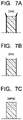
- FIG. 7A to FIG. 7F are views illustrating corner portion shapes of patterns after etching of etch masks used in Reference Example 1 and Comparative Example 1;
- FIG. 8 is a diagram illustrating an organic polymer used as an etch mask in Example 2.
- FIG. 9 is a diagram illustrating an organic polymer used as an etch mask in Comparative Example 3.
- FIG. 10 is a diagram illustrating a chemical compound which can replace a part of the organic polymer used in Example 2.
- FIG. 11 is a diagram illustrating a chemical compound which can replace a part of the organic polymer used in Example 2.
- FIG. 1 are cross-sectional views illustrating a process of the method of forming the pattern of the embodiment.
- a film to be processed 2 having been formed on a substrate 1 is prepared, and an etch mask 3 is formed on the film to be processed 2 by using a pattern-forming material containing a specific organic polymer.
- the film to be processed 2 is not particularly limited and various functional films are applicable.
- the etch mask 3 will be described in detail later.
- a resist pattern 4 is formed on the etch mask 3 .
- the resist pattern 4 is formed by forming a resist film on the etch mask 3 and then patterning the resist film by using a photo, electron beam or imprint lithography technology, or the like.
- a resist is dropped on the etch mask 3 , a template where a fine pattern is formed is pressed to the resist film, and the resist film is cured by irradiation of ultraviolet ray, to thereby form the resist pattern 4 .
- FIG. 1C illustrates the etch mask 3 having been patterned.
- a silicon oxide (SiO 2 ) film or the like may be interposed between the resist film and the etch mask 3 , so that the etch mask 3 may be patterned with the resist film and the SiO 2 film being used as a mask.
- the resist pattern 4 is removed, to thereby bring about a structure (pattern-forming body) 5 where the patterned etch mask 3 is provided on the film to be processed 2 .
- the pattern-forming body 5 is used for patterning the film to be processed 2 as illustrated in FIG. 1E .
- the film to be processed 2 is exposed to an etch gas and dry-etched via the patterned etch mask 3 . Thereby, the patterned film to be processed 2 is obtained.
- etch gas a gas containing a fluorine (F) atom is used.
- the etch gas contains fluorine (F) as fluorocarbon whose carbon number is 1 or more and 6 or less (C n F 2n+2 , C n F 2n , C n F 2n ⁇ 2 : n is a number of 1 or more and 6 or less), for example.
- the etch gas preferably further contains oxygen (O 2 ).
- the fluorine atom is preferably contained more than 1:1 (atom:atom) in terms of proportion of the fluorine atom to the oxygen atom.
- argon (Ar) or nitrogen (N 2 ) may be added as necessary. On this occasion, Ar or N 2 is not included in the proportion of the fluorine atom to the oxygen atom.
- an organic polymer constituted by 70 atom % or more carbon atoms having an sp 2 orbital (hereinafter, also referred to as sp 2 carbon atoms) and 5 atom % or more carbon atoms having an sp 3 orbital (hereinafter, also referred to as sp 3 carbon atoms) among the carbon atoms constituting the organic polymer contained in the pattern-forming material, and such a pattern-forming material is applied to an etch mask.
- etch mask even in a case where a film to be processed 2 is patterned by using an etch gas containing a fluorine (F) atom, a shape of a mask pattern can be maintained both during etching and after etching.
- F fluorine
- FIG. 2 illustrate cross-sectional views of the mask pattern before and after shoulder-drop occurs in the etch mask 3 .
- FIG. 2A illustrates a state where a mask pattern 3 P is formed on a film to be processed 2
- FIG. 2B illustrates a state where the film to be processed 2 has been processed by etching with the mask pattern 3 P being used as a mask.
- the mask pattern 3 P is in a state where a corner portion C of a cross-section upper edge is lacking, and such a state is referred to as a state where the shoulder-drop has occurred.
- the shoulder-drop occurs in the mask pattern 3 P, a problem such as a deterioration of a dimensional accuracy of the film to be processed 2 arises.
- the above-described configuration is applied to a molecular structure of an organic polymer contained in a pattern-forming material to become the etch mask 3 P, whereby occurrence of the shoulder-drop is suppressed.
- the present inventors have found out a problem that the shoulder-drop of the mask pattern 3 P as illustrated in FIG. 2B is likely to occur as etch resistance of the mask material is enhanced in a dry-etching process. Shoulder drop occurs when the mask pattern is attacked by accelerated ions, the etch rate of the corner portion (shoulders portion) of the pattern increases, and its shape cannot be maintained by being scraped from the shoulder portion during the etching. For example, when a processing of high aspect ratio such as for a 3-dimensional device is required, the above-described shoulder-drop is quite a serious problem.
- a mechanism of the etching by using the gas which contains the fluorine-based gas and the oxygen gas, RIE in particular, can be broken down into mainly three constituting factors of a chemical reaction by oxygen, a chemical reaction by fluorine (halogen), and sputtering by a physical collision by particles having high energy.
- etch resistance which has been studied, there are suggested measures such as improvement of oxygen resistance by introducing metal into a mask material to acquire flame retardancy, improvement of halogen resistance by raising a composition ratio of carbon atoms to oxygen atoms in the mask material (Ohnishi Parameter: J. Electrochem. Soc. vol. 130, 143, 1983), and so on, and it is known that these measures exhibit effects on improvement of the etch resistance.
- these measures do not improve sputtering resistance, and on the contrary, sometimes aggravate shoulder-drop, so that a solution has been desired.
- a sputtering mechanism can be explained by a cascade theory which is logically clarified by Sigmund et al. (Sigmund, Physical Review, 184, 383, 1969).
- Bond energy between atoms.
- ions incident at lower energy than the bond energy sputtering does not occur (threshold energy).
- ions incident from a tangential direction high-angle incidence
- ions incident from a normal direction low-angle incidence
- RIE a gas and a by-product of the gas and redeposition of an atom, a molecule, or the like which has been hit by etching are also important factors.
- deposition of F radical, CF 2 radical, or the like often occurs. It is known that consequently progress of etching is delayed or halted.
- a film thickness is decreased by the etching.
- pattern-forming materials having etch resistance of the same level there are materials which are likely to be subjected to shoulder-drop and materials which maintain the shapes of corner portions and unlikely to be subjected to shoulder-drop. This is because of an influence of a deposition substance such as a CF x -based substance or the like generated in the RIE.
- a substance substantially affecting a plasma process is CF 2 radical (Hori et al., J. Vac. Sci. Technol. A 16 233 1998).
- fluorine forms a chemical bond in some way and deposits on a polymer or the like.
- whether or not fluorine replaces an element constituting the polymer and is fixed can be found by comparing differences in bond energy between the elements.
- a material on which a fluorine atom is likely to deposit can be designed based on this understanding.
- a pattern-forming material containing an organic polymer excellent also in etch resistance in addition to the above-described characteristic.
- alkane is inferior in etch resistance regardless of being in a ring shape or being in a chain shape. Therefore, a main portion of the organic polymer used in the method of forming the pattern of the embodiment is desirable to be constituted by the aromatic ring or the like.
- the polymer constituted by the aromatic ring has high dry-etch resistance, a corner portion of a pattern tends to be easily shaved and that polymer is inferior in view of shoulder-drop.
- shoulder-drop is considered to be able to be reduced by constituting a main chain portion of an organic polymer basically by an aromatic ring to maintain high dry-etch resistance, and, for example, by adding alkane or the like on an outer side of a polymer chain as an antenna capable of catching a fluorine atom.
- a specific organic polymer contained in the pattern-forming material of the etch mask is constituted by 70 atom % or more carbon atoms having an sp 2 orbital (hereinafter, also referred to as “sp 2 carbon atom”) and 5 atom % or more carbon atoms having an sp 3 orbital (hereinafter, also referred to as “sp 3 carbon atom”) in relation to all the carbon atoms.
- the carbon atoms of the aromatic ring constitute double bonds of the sp 2 carbon atom. A bonding force between the carbon atoms is strong and the aromatic ring is excellent in dry-etch resistance.
- the carbon atoms constituting the organic polymer are preferable to be constituted by mainly the carbon atoms having the sp 2 orbital.
- Carbon having the sp 2 orbital may include sp 2 carbon atoms of a carbonyl group (—C( ⁇ O)—), a carboxyl group (—C( ⁇ O)—O—H), and a bivalent group (—C( ⁇ O)—O—) based thereon.
- the sp 2 carbon atoms are preferable to make up 70 atom % or more of all carbon. Further, increasing the proportion to 85 atom % or more further improves the dry-etch resistance.
- alkane since the carbon atoms of alkane are linearly connected by an sp 3 orbital and a bond of carbon-carbon is a single bond, a bonding force is relatively weak. Therefore, alkane is inferior in etch resistance. Note that the bonding by the sp 3 orbital exhibits high dry-etch resistance in three-dimensional network such as diamond and diamond-like carbon. Though the sp 3 carbon atoms constituting alkane may be smaller in number compared with the sp 2 carbon atoms, it is preferable that 5 atom % or more sp 3 carbon atoms are contained in relation to all the carbon atoms constituting the organic polymer.
- alkane exists on a surface of a polymer chain
- alkane is likely to react with fluorine to form fluoride by a steric effect.
- a carbon atom which is apart by 4 or more in the number of atoms from a constituent atom constituting a main chain is preferable to be the sp 3 carbon atom.
- hydrogen is likely to be replaced with fluoride by the steric effect, so that an effect of maintaining the shape of the pattern after etching can be enhanced.
- the etch mask 3 used in the method of forming the pattern of the embodiment contains the organic polymer in the pattern-forming material used for forming the etch mask 3 , and contains 70 atom % or more carbon atoms having the sp 2 orbital and 5 atom % or more carbon atoms having the sp 3 orbital among the carbon atoms constituting the organic polymer. It is further desirable that 80 atom % or more carbon atoms having the sp 2 orbital are contained for the sake of improvement of etch resistance.
- the etch mask 3 may be an organic film constituted only by the above-described organic polymer or may be a later-described composite film obtained by infiltrating an organic film with a metallic compound.
- a process of constituting a organo-metalic material composite body by infiltrating an organic film with a metallic compound is referred to as metallization.
- metallization A process of constituting a organo-metalic material composite body by infiltrating an organic film with a metallic compound. Note that a part of carbon atoms contained in the organic material may be a carbon atom having an sp orbital.
- FIG. 3 and FIG. 4 illustrate examples of organic polymers contained in the pattern-forming material used for forming the etch mask by the method of forming the pattern of the embodiment.
- the organic polymer containing 70 atom % or more sp 2 carbon atoms include a polymer containing an aromatic ring as a main chain, as illustrated in FIG. 3 , for example.
- the aromatic ring is not limited to the benzene ring and may be a polycyclic aromatic ring such as a naphthalene ring and an anthracene ring, as illustrated in FIG. 3 .
- the polycyclic aromatic ring may be a pyrene ring.
- R 1 includes any one of an alkyl chain (—CH 2 —), ether (—O—), ester (—C( ⁇ O)—O—), amide (—C( ⁇ O)—NH—)), imide (—C( ⁇ O)—NH—C( ⁇ O)), and sulfonyl (—SO 2 —), or, sometimes an atom is not placed.
- R 2 includes any one of an aromatic ring, a hydroxyl group (—OH), a carboxyl group (—COOH), an amino group (—NH 2 ), a nitro group (—NO 2 ) and a sulfonic group (—SO 2 OH), or is a hydrogen atom (—H).
- R 3 indicates an alkyl group having a straight chain or a branch or a cycloalkyl group of the embodiment in which the carbon number is 1 or more and 6 or less.
- R 4 includes any one of a hydrogen atom, a halogen atom, a methyl group, and an ethyl group
- R 5 includes any one of an alkyl chain (—CH 2 —), ether (—O—), ester (—C( ⁇ O)—O—), amide (—C( ⁇ O)—NH—)), imide (—C( ⁇ O)—NH—C( ⁇ O)), and sulfonyl (—SO 2 —), or, sometimes an atom is not placed.
- R 6 indicates an alkyl group having a straight chain or a branch or a cycloalkyl group of the embodiment in which the carbon number is 1 or more and 6 or less.
- the organic polymer of the embodiment the polymers illustrated in FIG. 3 and FIG. 4 can be used independently, but in general, a copolymer obtained by combining these is used in order to fulfil improvement of various necessary properties.
- the pattern-forming material of the embodiment may contain a material other than the organic polymer.
- the pattern-forming material of the embodiment may be an organic film constituted only by the above-described organic polymer and may be a later-described composite film obtained by infiltrating an organic film with a metallic compound.
- the pattern-forming material of the embodiment may contain materials other than the organic polymer. In that case, it suffices that the organic polymer makes up 70 wt % or more of the pattern-forming material except a solvent.
- the side chain of the organic polymer may contain not only the aromatic ring or the hydrocarbon group, but also a hydroxyl group (—OH), a carboxyl group (—COOH), an amino group (—NH 2 ), a nitro group (—NO 2 ), sulfonic acid (—SO 2 OH), or the like, and may further contain an alkyl group (—C n H n+2 ).
- the organic polymer may be a material obtained by bonding an aromatic ring to a main chain constituted by an aliphatic hydrocarbon group (—CH 2 —, or the like), such as polystyrene, for example.
- a main chain constituted by an aliphatic hydrocarbon group (—CH 2 —, or the like) such as polystyrene, for example.
- it is preferable that in the organic polymer 80 atom % or more of the sp 2 carbon atoms is constituted by the aromatic rings.
- the aforementioned group containing the sp 3 carbon atom is preferable to contain carbon apart by 4 or more in the number of atoms from the atom constituting the main chain.
- FIG. 5 explains details of the “number of atoms from the main chain” defined in the embodiment.
- the numeral in FIG. 5 indicates the “number of atoms” from the atom in a connecting portion of the main chain, and indicates the “number of atoms from the main chain” of the embodiment.
- the “atom” is often a carbon atom, but may be an atom other than a hydrogen atom which constitutes a general organic compound, such as a nitrogen atom, an oxygen atom, and a sulfur atom.
- the carbon atom may be the sp 2 carbon atom or sp 3 carbon atom.
- a polymer chain is a long chain, which intertwines randomly as a thread. Therefore, when a molecule such as a precursor comes from the outside, the molecule is hard to approach the atom close to the main chain. When the atom is far from the main chain, steric hindrance is relieved, so that deposition/substitution reaction of the fluorine atom, which is a mechanism of the embodiment, becomes likely to occur.
- Those aspects can be calculated by using a molecular orbital method or a molecular dynamics method.
- the hydrogen atom added to the sp 3 carbon atom contained in the main chain or the sp 3 carbon atom close to the main chain has a low probability of being replaced with the fluorine atom.
- the hydrogen atom added to the sp 3 carbon atom far from the main chain can be easily replaced with the fluorine atom.
- the organic polymer is preferable to be constituted by an alkyl group which has a linear chain or a branch or a cycloalkyl group.
- R 3 or R 6 indicates the alkyl group or the cycloalkyl group.
- the alkyl group may have either one of a linear-chain structure and a structure with a branch. Both of these groups contain the sp 3 carbon atom, and replacement of a hydrogen atom with a fluorine atom is likely to occur in an etching process by using an etch gas containing fluorocarbon or the like.
- the group containing sp a carbon atom is preferable to be an alkyl group or a cycloalkyl group whose carbon number is 1 or more and 6 or less.
- metallization of an organic film will be described.
- metallization of the etch mask 3 as the patterned organic film illustrated in FIG. 1D brings about a metallized etch mask (mask pattern) 3 .
- Metallization of the organic film is performed as follows, for example. A stack obtained by forming a film to be processed 2 and an organic film 3 sequentially on a substrate 1 is carried in a vacuum device and the organic film 3 is exposed to a gas or a liquid of a metallic compound such as trimethylaluminum (TMA) as a metal-containing fluid.
- TMA trimethylaluminum
- a molecule of the metallic compound is absorbed by a carbonyl group or the like in the organic film 3 , for example, and a terminal group (hydrocarbon group, for example) of the carbonyl group is eliminated. Then, a structure in which a metallic compound (Al(CH 3 ) x ) or the like is bonded firmly with an oxygen atom in the organic film 3 is formed.
- An exposure treatment of the metallic compound to the organic film 3 is preferable to be performed under heating. A heating temperature is appropriately selected in accordance with the kind of the metallic compound and the kind of an organic material constituting the organic film 3 .
- a metallic compound used in a CVD method or an atomic layer deposition (ALD) method can be used without limitation in particular.
- metal contained in the metallic compound include aluminum, titanium, tungsten, vanadium, hafnium, zirconium, tantalum, molybdenum, and so on.
- the organic metallic compound and halide thereof one having a sufficiently small ligand is usable as the metallic compound.
- the usable metallic compounds include AlCl 3 , TiCl 4 , WCl 6 , VCl 4 , HfCl 4 , ZrCl 4 , Al(CH 3 ) 3 , and so on.
- Metallization of the organic film may be performed not only in a gas phase but also in a liquid phase.
- FIG. 6 are cross-sectional views illustrating a process of the method of manufacturing the semiconductor device of the embodiment.
- a film to be processed 12 is formed on a semiconductor substrate 11 .
- the film to be processed 12 is a stacked film obtained by alternately stacking silicon nitride 13 and a silicon oxide film 14 , for example.
- the stacked film is used for manufacturing a three-dimensionally stacked nonvolatile memory device which has a memory cell of a vertical transistor structure, for example.
- An etch mask 3 for which a pattern-forming material containing a specific organic polymer is used is formed on the film to be processed 12 made of the above stacked film.
- the etch mask 3 is similar to the aforementioned etch mask used in the method of forming the pattern of the embodiment described above.
- a resist pattern 4 is formed on the etch mask 3 .
- the resist pattern 4 is formed by patterning a resist film formed on the etch mask 3 , by using a photo, electron beam or imprint lithography technology, or the like similarly to the method of forming the pattern of the embodiment.
- the etch mask 3 is etch-processed by dry-etching, to thereby be patterned.
- the film to be processed 12 is exposed to an etch gas via the patterned etch mask 3 , to thereby be dry-etched. By such dry-etching, the film to be processed 12 having been patterned is obtained as illustrated in FIG. 6E .
- etch gas a gas containing a fluorine atom (F) is used. It is preferable that the etch gas contains fluorine (F) as fluorocarbon whose carbon number is 1 or more and 6 or less (C n F 2n+2 , C n F 2n , C n F 2n ⁇ 2 : n is a number of 1 or more and 6 or less), for example.
- the etch gas is preferable to further contain an oxygen gas (O 2 ).
- the fluorine atom is contained more than 1:1 (atom:atom) in terms of proportion of the fluorine atom to the oxygen. Usage of such an etch gas containing the fluorocarbon and so on enables effective etching of the above-described film to be processed 12 such as the stacked film.
- the film to be processed 12 is not limited to the above-described stacked film but various films are applicable.
- the film to be processed 12 having been patterned which is illustrated in FIG. 6E is applied to production of a memory cell array, by using a known method, for example.
- a hole pattern (memory hole) is formed in a stacked film by the above-described processing.
- a block insulation layer, a charge storage layer, a tunnel insulation layer, a channel layer, and a core layer are sequentially formed in that memory hole.
- only a nitride film among the stacked film is removed via a slit formed separately from the memory hole, and a conductive film is embedded in a space generated by the removal.
- the conductive film in the stacked film can be made to function as a word line.
- MPM 4-methylphenyl methacrylate
- MPA 4-methylphenyl acrylate
- GM glycidyl methacrylate
- Citric acid is mixed as a counterpart crosslinking agent to GM being a crosslinking group of those polymers, and a mixture is dissolved in a cyclohexanone solvent.
- GM and citric acid is mixed so that a molar ratio of glycidyl groups of GM and carbonyl groups of citric acid may be equal in a molar ratio.
- Spin-coating and annealing are carried out to perform crosslinking.
- a line-and-space (L/S) pattern and a contact hole (CH) pattern are impressed by using an i-line exposure unit, and development is carried out with a tetramethylammonium hydroxide (TMAH) aqueous solution, to thereby perform patterning.
- TMAH tetramethylammonium hydroxide
- O 2 RIE is performed, the above-described polymer film is etched to transfer the pattern, and thereafter, the resist is removed with the PGMEA solvent.
- FIG. 7A to FIG. 7F illustrate pattern shapes after etching of each sample.
- a portion shown by a thick line indicates deposition by etching, for example.
- the excessively extended alkyl group causes deterioration of etch resistance, which is quite important. Therefore, the carbon number of the alkyl group is preferable to be 6 or less. Further, when RIE is carried out with a mixed gas of a fluorine-based gas and an oxygen gas, a similar tendency can be obtained.
- styrene-based resin is applied.
- PS polystyrene
- P4MS poly(4-methylstyrene)
- PVN poly(2-vinylnaphtalene)
- PVN poly(2-phenyl-6-methylnaphthalene)
- P6MVN poly(2-phenyl-6-methylnaphthalene)
- 2 mol % GM is copolymerized as a crosslinking group.
- AIBN azobis(isobutyronitrile)
- THF tetrahydrofuran
- JSR NSC SOG270-61 is applied in a thickness of 50 nm as SOG, and the SOG is cured at 200° C. Further, thereon, an i-line resist (Fuji, FHi-672B) is applied in a thickness of 0.4 ⁇ m.
- a line-and-space (L/S) pattern and a contact hole (CH) pattern are impressed by using an i-line exposure unit, and development is carried out with a TMAH aqueous solution to thereby perform patterning.
- O 2 RIE is performed, the above-described polymer film is etched to transfer the pattern, and thereafter, the resist is removed with the PGMEA solvent.
- Example 2 an organic compound having an aromatic ring structure is applied.
- Example 2 0.5 mol 2,2′-[methylenebis(1,2-naphtalenediyloxymethylene)]bis[oxirane] (CAS No.: 1059-93-4) and 1.0 mol 3-hydroxy-7-methyl-2-naphthalenecarboxylic acid (CAS No.: 143355-55-9) are dissolved in a 2-methoxy-1-propanol solution, 0.025 mol benzyltriethylammonium chloride is added, and a reaction is performed at 120° C. for 8 hours.
- a reaction product receives an addition of 1 L methylisobutylketone (MIBK) and is put into a separating funnel, and then is washed in pure water several times. An organic phase is dried under a reduced pressure, and an individual chemical compound (1) illustrated in FIG. 8 is retrieved.
- MIBK methylisobutylketone
- a crosslinking agent 1,3,4, 6-tetrakis(methoxymethyl) glycoluril (CAS No.: 17464-88-9) and tripropylammonium methyl trifluoromethanesulfonate (CAS No.: 1001324-50-0) are dissolved in a PGMEA solvent, and annealing is performed at 250° C. for 60 seconds. The presence of PGMEA solvent resistance is confirmed by this annealing at 250° C. or more. A film thickness is adjusted to be about 1.0 ⁇ m by a concentration and a rotation number. Thereon, JSR NSC SOG270-61 is applied in a thickness of 50 nm as SOG, and the SOG is cured at 200° C.
- an i-line resist (Fuji, FHi-672B) is applied in a thickness of 0.4 ⁇ m.
- a line-and-space (L/S) pattern and contact hole (CH) pattern are impressed by using an i-line exposure unit, and development is carried out with a TMAH aqueous solution to thereby perform patterning.
- O 2 RIE is performed, the above-described polymer film is etched to transfer the pattern, and thereafter, the resist is removed with the PGMEA solvent.
- a toluene solution of Tetrakis(triphenylphosphine)palladium(0) is added and a mixture is fluxed for 10 hours. After precipitation with methanol, filtration is performed. Further, a filtered product is washed with pure water and thereafter redissolved in methylene chloride. An obtained solution is dried and a polymer A illustrated in FIG. 12 is obtained.
- 1,1′:4′,1′′-Terphenyl,4,4′′-bis(1,1-dimethylethyl)-2′,5′-diiodo-(CAS: 959712-69-7) is synthesized in accordance with a literature (J. Am. Chem. Soc., 2007, 129, 14116).
- a literature J. Am. Chem. Soc., 2007, 129, 14116.
- 2′,5′-Diiodo-1,1′:4′,1′′-terphenyl Similar polymerization is performed and a polymer B illustrated in FIG. 12 is obtained.
- the obtained polymer A and polymer B are dissolved in toluene and spin-coating is performed.
- JSR NSC SOG270-61 is applied in a thickness of 50 nm as spin on glass (SOG), and the SOG is cured at 200° C.
- an i-line resist (Fuji, FHi-672B) is applied in a thickness of 0.4 ⁇ m.
- a line-and-space (L/S) pattern and a contact hole (CH) pattern are impressed by using an i-line exposure unit, and development is carried out with a tetramethylammonium hydroxide (TMAH) aqueous solution, to thereby perform patterning.
- TMAH tetramethylammonium hydroxide
- the structures illustrated in FIG. 13 also exhibit similar properties.
- R 7 and R 8 may be the same or different, being hydrogen, a hydroxyl group, a carboxyl group, a formyl group, or an alkyl group whose carbon number is 1 to 6.
- R 9 and R 10 may be the same or different, being an alkyl group whose carbon number is 1 to 6.
- R 11 and Ru may be the same or different, being hydrogen or a phenyl group.
Landscapes
- Chemical & Material Sciences (AREA)
- Organic Chemistry (AREA)
- Health & Medical Sciences (AREA)
- Materials Engineering (AREA)
- Wood Science & Technology (AREA)
- Engineering & Computer Science (AREA)
- Life Sciences & Earth Sciences (AREA)
- Chemical Kinetics & Catalysis (AREA)
- Medicinal Chemistry (AREA)
- Polymers & Plastics (AREA)
- Drying Of Semiconductors (AREA)
- Photosensitive Polymer And Photoresist Processing (AREA)
- Materials For Photolithography (AREA)
Abstract
Description
Claims (3)
Applications Claiming Priority (3)
| Application Number | Priority Date | Filing Date | Title |
|---|---|---|---|
| JP2020-051206 | 2020-03-23 | ||
| JPJP2020-051206 | 2020-03-23 | ||
| JP2020051206A JP7383540B2 (en) | 2020-03-23 | 2020-03-23 | Pattern forming method, semiconductor device manufacturing method, and pattern forming material |
Publications (2)
| Publication Number | Publication Date |
|---|---|
| US20210296116A1 US20210296116A1 (en) | 2021-09-23 |
| US11410848B2 true US11410848B2 (en) | 2022-08-09 |
Family
ID=77748462
Family Applications (1)
| Application Number | Title | Priority Date | Filing Date |
|---|---|---|---|
| US16/997,115 Active US11410848B2 (en) | 2020-03-23 | 2020-08-19 | Method of forming pattern, method of manufacturing semiconductor device, and pattern-forming material |
Country Status (2)
| Country | Link |
|---|---|
| US (1) | US11410848B2 (en) |
| JP (1) | JP7383540B2 (en) |
Families Citing this family (4)
| Publication number | Priority date | Publication date | Assignee | Title |
|---|---|---|---|---|
| JP2023045177A (en) | 2021-09-21 | 2023-04-03 | キオクシア株式会社 | Indium-containing organic polymer film manufacturing method, pattern forming method, and semiconductor device manufacturing method |
| US12308290B2 (en) | 2022-05-17 | 2025-05-20 | Nanya Technology Corporation | Method for preparing semiconductor device structure with fluorine-catching layer |
| TWI825823B (en) * | 2022-05-17 | 2023-12-11 | 南亞科技股份有限公司 | Method for fabricating semiconductor device structure with fluorine-catching layer |
| US12308319B2 (en) | 2022-05-17 | 2025-05-20 | Nanya Technology Corporation | Semiconductor device structure with fluorine-catching layer |
Citations (13)
| Publication number | Priority date | Publication date | Assignee | Title |
|---|---|---|---|---|
| US6147407A (en) * | 1998-03-27 | 2000-11-14 | Lucent Technologies Inc. | Article comprising fluorinated amorphous carbon and process for fabricating article |
| US20090017318A1 (en) * | 2006-02-23 | 2009-01-15 | Picodeon Ltd Oy | Coating on a metal substrate and a coated metal product |
| US8394244B1 (en) * | 2009-09-24 | 2013-03-12 | Applied Micro Circuits Corporation | System and method for laser patterning an integrated circuit etching mask |
| US9743885B1 (en) * | 2014-06-12 | 2017-08-29 | Verily Life Sciences Llc | Method of two-step parylene patterning and etching to release a parylene sandwiched device |
| US20180275519A1 (en) | 2017-03-22 | 2018-09-27 | Toshiba Memory Corporation | Pattern Formation Method |
| JP2019023251A (en) | 2017-07-21 | 2019-02-14 | 信越化学工業株式会社 | Organic film forming composition, pattern forming method, and organic film forming resin |
| US20190259606A1 (en) | 2018-02-22 | 2019-08-22 | Toshiba Memory Corporation | Pattern-forming method |
| US20200012187A1 (en) | 2018-07-06 | 2020-01-09 | Toshiba Memory Corporation | Pattern forming method and semiconductor device manufacturing method |
| JP2020002227A (en) | 2018-06-27 | 2020-01-09 | キオクシア株式会社 | Pattern forming material, pattern forming method, and semiconductor device manufacturing method |
| US20200291156A1 (en) * | 2019-03-11 | 2020-09-17 | Toshiba Memory Corporation | Polymer material, composition, and method of manufacturing semiconductor device |
| US20200291155A1 (en) | 2019-03-11 | 2020-09-17 | Toshiba Memory Corporation | Pattern forming material, composition for pattern formation, pattern forming method and method of manufacturing semiconductor device |
| JP2020149037A (en) | 2019-03-11 | 2020-09-17 | キオクシア株式会社 | Pattern forming material, pattern forming composition, pattern forming method and manufacturing method of semiconductor device |
| US20210082693A1 (en) | 2019-09-18 | 2021-03-18 | Kioxia Corporation | Method of forming pattern and method of manufacturing semiconductor device |
Family Cites Families (4)
| Publication number | Priority date | Publication date | Assignee | Title |
|---|---|---|---|---|
| JPS6279446A (en) * | 1985-10-03 | 1987-04-11 | Kuraray Co Ltd | Crosslinkable copolymer and positive type resist composed of its copolymer |
| JP2003249437A (en) * | 2002-02-26 | 2003-09-05 | Sony Corp | Pattern forming method and semiconductor device manufacturing method |
| EP2479198B1 (en) * | 2009-09-15 | 2016-02-17 | Mitsubishi Gas Chemical Company, Inc. | Aromatic hydrocarbon resin and composition for forming underlayer film for lithography |
| KR102287813B1 (en) * | 2014-05-30 | 2021-08-10 | 삼성전자주식회사 | Hardmask composition and method of forming patterning using the hardmask composition |
-
2020
- 2020-03-23 JP JP2020051206A patent/JP7383540B2/en active Active
- 2020-08-19 US US16/997,115 patent/US11410848B2/en active Active
Patent Citations (20)
| Publication number | Priority date | Publication date | Assignee | Title |
|---|---|---|---|---|
| US6147407A (en) * | 1998-03-27 | 2000-11-14 | Lucent Technologies Inc. | Article comprising fluorinated amorphous carbon and process for fabricating article |
| US20090017318A1 (en) * | 2006-02-23 | 2009-01-15 | Picodeon Ltd Oy | Coating on a metal substrate and a coated metal product |
| US8394244B1 (en) * | 2009-09-24 | 2013-03-12 | Applied Micro Circuits Corporation | System and method for laser patterning an integrated circuit etching mask |
| US9743885B1 (en) * | 2014-06-12 | 2017-08-29 | Verily Life Sciences Llc | Method of two-step parylene patterning and etching to release a parylene sandwiched device |
| US20180275519A1 (en) | 2017-03-22 | 2018-09-27 | Toshiba Memory Corporation | Pattern Formation Method |
| JP2018160537A (en) | 2017-03-22 | 2018-10-11 | 東芝メモリ株式会社 | Pattern formation method |
| JP2019023251A (en) | 2017-07-21 | 2019-02-14 | 信越化学工業株式会社 | Organic film forming composition, pattern forming method, and organic film forming resin |
| US10615045B2 (en) | 2017-07-21 | 2020-04-07 | Shin-Etsu Chemical Co., Ltd. | Composition for forming organic film, patterning process, and resin for forming organic film |
| US20190259606A1 (en) | 2018-02-22 | 2019-08-22 | Toshiba Memory Corporation | Pattern-forming method |
| JP2019145714A (en) | 2018-02-22 | 2019-08-29 | 東芝メモリ株式会社 | Patterning method |
| JP2020002227A (en) | 2018-06-27 | 2020-01-09 | キオクシア株式会社 | Pattern forming material, pattern forming method, and semiconductor device manufacturing method |
| US10672621B2 (en) | 2018-06-27 | 2020-06-02 | Toshiba Memory Corporation | Pattern forming material, pattern forming method, and method for manufacturing semiconductor device |
| JP2020009869A (en) | 2018-07-06 | 2020-01-16 | キオクシア株式会社 | Pattern forming method and semiconductor device manufacturing method |
| US20200012187A1 (en) | 2018-07-06 | 2020-01-09 | Toshiba Memory Corporation | Pattern forming method and semiconductor device manufacturing method |
| US20200291156A1 (en) * | 2019-03-11 | 2020-09-17 | Toshiba Memory Corporation | Polymer material, composition, and method of manufacturing semiconductor device |
| US20200291155A1 (en) | 2019-03-11 | 2020-09-17 | Toshiba Memory Corporation | Pattern forming material, composition for pattern formation, pattern forming method and method of manufacturing semiconductor device |
| JP2020147633A (en) | 2019-03-11 | 2020-09-17 | キオクシア株式会社 | Method for manufacturing polymer materials, compositions and semiconductor devices |
| JP2020149037A (en) | 2019-03-11 | 2020-09-17 | キオクシア株式会社 | Pattern forming material, pattern forming composition, pattern forming method and manufacturing method of semiconductor device |
| US20210082693A1 (en) | 2019-09-18 | 2021-03-18 | Kioxia Corporation | Method of forming pattern and method of manufacturing semiconductor device |
| JP2021048257A (en) | 2019-09-18 | 2021-03-25 | キオクシア株式会社 | Pattern formation method and semiconductor device manufacturing method |
Non-Patent Citations (3)
| Title |
|---|
| Coburn et al., "Plasma etching—A discussion of mechanisms," J. Vac. Sci. Technol. (Mar./Apr. 1979), 16:391-403. |
| K. Nojiri, "Dry Etching Technology for Semiconductors, Chapter 2: Mechanism of Dry Etching" Springer International Publishing (2015), pp. 11-30. |
| Negishi et al., "Deposition control for reduction of 193 nm photoresist degradation in dielectric etching,": J. Vac. Sci. Technol. B (Jan/Feb. 2005), 23:217-223. |
Also Published As
| Publication number | Publication date |
|---|---|
| JP7383540B2 (en) | 2023-11-20 |
| JP2021150589A (en) | 2021-09-27 |
| US20210296116A1 (en) | 2021-09-23 |
Similar Documents
| Publication | Publication Date | Title |
|---|---|---|
| US11410848B2 (en) | Method of forming pattern, method of manufacturing semiconductor device, and pattern-forming material | |
| JP6906107B2 (en) | Hydrofluorocarbons containing -NH2 functional groups for 3D NAND and DRAM applications | |
| TWI850421B (en) | Composition for forming organic film, patterning process, and polymer | |
| CN115877657B (en) | Organic film forming composition, pattern forming method, and organic film forming compound and polymer | |
| US11177129B2 (en) | Method of manufacturing semiconductor device, method of forming pattern film, and metal-containing organic film | |
| CN111681952B (en) | Substrate processing equipment | |
| US12379662B2 (en) | Material for forming organic film, patterning process, compound, and polymer | |
| US20240402596A1 (en) | Compound For Forming Metal-Containing Film, Composition For Forming Metal-Containing Film, And Patterning Process | |
| US20240248404A1 (en) | Compound For Forming Metal-Containing Film, Composition For Forming Metal-Containing Film, And Patterning Process | |
| US11393671B2 (en) | Method of forming pattern and method of manufacturing semiconductor device | |
| US20220221792A1 (en) | Pattern forming material and pattern forming method | |
| US20250087495A1 (en) | Compound For Forming Metal-Containing Film, Composition For Forming Metal-Containing Film, And Patterning Process | |
| US20250085636A1 (en) | Compound For Forming Metal-Containing Film, Composition For Forming Metal-Containing Film, And Patterning Process | |
| EP3739388B1 (en) | Composition for forming organic film, patterning process, and polymer | |
| US20240295816A1 (en) | Compound For Forming Metal-Containing Film, Composition For Forming Metal-Containing Film, And Patterning Process | |
| EP4390548A1 (en) | Compound for forming metal-containing film, composition for forming metal-containing film, and patterning process | |
| CN116693361B (en) | Composition for forming organic film, pattern forming method, and compound | |
| US11257684B2 (en) | Method of dry etching copper thin film | |
| CN111675783B (en) | Pattern forming material, composition for pattern formation, pattern forming method, and method for manufacturing semiconductor device | |
| US20250036029A1 (en) | Method For Forming Resist Underlayer Film And Patterning Process | |
| US20250060670A1 (en) | Method For Forming Resist Underlayer Film And Patterning Process | |
| US12228860B2 (en) | Compound, polymer, pattern forming material, pattern forming method, and method of manufacturing semiconductor device | |
| US20240345483A1 (en) | Method For Forming Resist Underlayer Film And Patterning Process | |
| KR102942477B1 (en) | Compound for forming metal-containing film, composition for forming metal-containing film, and patterning process | |
| CN116136644A (en) | Composition for forming organic film, method for forming pattern, compound and polymer for forming organic film |
Legal Events
| Date | Code | Title | Description |
|---|---|---|---|
| AS | Assignment |
Owner name: KIOXIA CORPORATION, JAPAN Free format text: ASSIGNMENT OF ASSIGNORS INTEREST;ASSIGNORS:ASAKAWA, KOJI;SASAO, NORIKATSU;SUGIMURA, SHINOBU;REEL/FRAME:053537/0250 Effective date: 20200716 |
|
| FEPP | Fee payment procedure |
Free format text: ENTITY STATUS SET TO UNDISCOUNTED (ORIGINAL EVENT CODE: BIG.); ENTITY STATUS OF PATENT OWNER: LARGE ENTITY |
|
| STPP | Information on status: patent application and granting procedure in general |
Free format text: NON FINAL ACTION MAILED |
|
| STPP | Information on status: patent application and granting procedure in general |
Free format text: RESPONSE TO NON-FINAL OFFICE ACTION ENTERED AND FORWARDED TO EXAMINER |
|
| STPP | Information on status: patent application and granting procedure in general |
Free format text: NOTICE OF ALLOWANCE MAILED -- APPLICATION RECEIVED IN OFFICE OF PUBLICATIONS |
|
| STCF | Information on status: patent grant |
Free format text: PATENTED CASE |
|
| MAFP | Maintenance fee payment |
Free format text: PAYMENT OF MAINTENANCE FEE, 4TH YEAR, LARGE ENTITY (ORIGINAL EVENT CODE: M1551); ENTITY STATUS OF PATENT OWNER: LARGE ENTITY Year of fee payment: 4 |