US11404384B2 - Interconnect structure - Google Patents
Interconnect structure Download PDFInfo
- Publication number
- US11404384B2 US11404384B2 US17/105,480 US202017105480A US11404384B2 US 11404384 B2 US11404384 B2 US 11404384B2 US 202017105480 A US202017105480 A US 202017105480A US 11404384 B2 US11404384 B2 US 11404384B2
- Authority
- US
- United States
- Prior art keywords
- conductive via
- conductive
- height
- distance
- insulating layer
- Prior art date
- Legal status (The legal status is an assumption and is not a legal conclusion. Google has not performed a legal analysis and makes no representation as to the accuracy of the status listed.)
- Active, expires
Links
Images


Classifications
-
- H01L23/552—
-
- H—ELECTRICITY
- H10—SEMICONDUCTOR DEVICES; ELECTRIC SOLID-STATE DEVICES NOT OTHERWISE PROVIDED FOR
- H10W—GENERIC PACKAGES, INTERCONNECTIONS, CONNECTORS OR OTHER CONSTRUCTIONAL DETAILS OF DEVICES COVERED BY CLASS H10
- H10W20/00—Interconnections in chips, wafers or substrates
- H10W20/40—Interconnections external to wafers or substrates, e.g. back-end-of-line [BEOL] metallisations or vias connecting to gate electrodes
- H10W20/41—Interconnections external to wafers or substrates, e.g. back-end-of-line [BEOL] metallisations or vias connecting to gate electrodes characterised by their conductive parts
- H10W20/43—Layouts of interconnections
-
- H—ELECTRICITY
- H10—SEMICONDUCTOR DEVICES; ELECTRIC SOLID-STATE DEVICES NOT OTHERWISE PROVIDED FOR
- H10W—GENERIC PACKAGES, INTERCONNECTIONS, CONNECTORS OR OTHER CONSTRUCTIONAL DETAILS OF DEVICES COVERED BY CLASS H10
- H10W20/00—Interconnections in chips, wafers or substrates
- H10W20/40—Interconnections external to wafers or substrates, e.g. back-end-of-line [BEOL] metallisations or vias connecting to gate electrodes
- H10W20/497—Inductive arrangements or effects of, or between, wiring layers
-
- H—ELECTRICITY
- H10—SEMICONDUCTOR DEVICES; ELECTRIC SOLID-STATE DEVICES NOT OTHERWISE PROVIDED FOR
- H10W—GENERIC PACKAGES, INTERCONNECTIONS, CONNECTORS OR OTHER CONSTRUCTIONAL DETAILS OF DEVICES COVERED BY CLASS H10
- H10W42/00—Arrangements for protection of devices
- H10W42/20—Arrangements for protection of devices protecting against electromagnetic or particle radiation, e.g. light, X-rays, gamma-rays or electrons
-
- H01L23/5226—
-
- H01L23/5283—
-
- H—ELECTRICITY
- H10—SEMICONDUCTOR DEVICES; ELECTRIC SOLID-STATE DEVICES NOT OTHERWISE PROVIDED FOR
- H10W—GENERIC PACKAGES, INTERCONNECTIONS, CONNECTORS OR OTHER CONSTRUCTIONAL DETAILS OF DEVICES COVERED BY CLASS H10
- H10W20/00—Interconnections in chips, wafers or substrates
- H10W20/40—Interconnections external to wafers or substrates, e.g. back-end-of-line [BEOL] metallisations or vias connecting to gate electrodes
- H10W20/41—Interconnections external to wafers or substrates, e.g. back-end-of-line [BEOL] metallisations or vias connecting to gate electrodes characterised by their conductive parts
- H10W20/42—Vias, e.g. via plugs
-
- H—ELECTRICITY
- H10—SEMICONDUCTOR DEVICES; ELECTRIC SOLID-STATE DEVICES NOT OTHERWISE PROVIDED FOR
- H10W—GENERIC PACKAGES, INTERCONNECTIONS, CONNECTORS OR OTHER CONSTRUCTIONAL DETAILS OF DEVICES COVERED BY CLASS H10
- H10W20/00—Interconnections in chips, wafers or substrates
- H10W20/40—Interconnections external to wafers or substrates, e.g. back-end-of-line [BEOL] metallisations or vias connecting to gate electrodes
- H10W20/41—Interconnections external to wafers or substrates, e.g. back-end-of-line [BEOL] metallisations or vias connecting to gate electrodes characterised by their conductive parts
- H10W20/435—Cross-sectional shapes or dispositions of interconnections
Definitions
- the present disclosure relates to an interconnect structure. More particularly, the present disclosure relates to an interconnect structure having a circuit structure that can prevent the noise interference from other circuit element.
- Integrated circuits are typically fabricated with multiple levels of patterned conductive lines, electrically separated from one another by the interlayer dielectric layer containing conductive vias at selected locations to provide electrical connections between levels of the patterned conductive lines.
- ICs integrated circuits
- RF radio-frequency
- EMI electromagnetic interference
- the present disclosure provides an interconnect structure including a first insulating layer, a first conductive line, a second insulating layer, a second conductive line, a first conductive via, a second conductive via, and a third conductive via.
- the first conductive line is embedded in the first insulating layer and includes a first portion and a second portion.
- the second insulating layer is disposed on the first insulating layer.
- the second conductive line is embedded in the second insulating layer and includes a third portion and a fourth portion.
- the first conductive via, the second conductive via, and the third conductive via are embedded in the first insulating layer.
- the first conductive via connects the first portion and the third portion.
- the second conductive via connects the second portion and the third portion.
- the third conductive via connects the second portion and the fourth portion.
- a first cross-sectional area surrounded by the first portion, the second portion, the third portion, the first conductive via, and the second conductive via is substantially equal to a second cross-sectional area surrounded by the second portion, the third portion, the fourth portion, the second conductive via, and third conductive via.
- the first cross-sectional area is substantially a height between the first portion and the third portion multiplied by a distance between the first conductive via and the second conductive via.
- the second cross-sectional area is substantially a height between the second portion and the fourth portion multiplied by a distance between the second conductive via and the third conductive via.
- a height between the first portion and the third portion is substantially equal to a distance between the first conductive via and the second conductive via.
- a height between the second portion and the fourth portion is substantially equal to a distance between the second conductive via and the third conductive via.
- a height between the first portion and the third portion is larger than a distance between the first conductive via and the second conductive via.
- a height between the second portion and the fourth portion is larger than a distance between the second conductive via and the third conductive via.
- a height between the first portion and the third portion is smaller than a distance between the first conductive via and the second conductive via.
- a height between the second portion and the fourth portion is smaller than a distance between the second conductive via and the third conductive via.
- the present disclosure provides an interconnect structure including a first insulating layer, a first conductive line, a second insulating layer, a second conductive line, a third insulating layer, a third conductive line, a first conductive via, a second conductive via, a third conductive via and a fourth conductive via.
- the first conductive line is embedded in the first insulating layer.
- the second insulating layer is disposed on the first insulating layer.
- the second conductive line is embedded in the second insulating layer and includes a first portion, a second portion, and a third portion.
- the third insulating layer is disposed on the second insulating layer.
- the third conductive line embedded in the third insulating layer is embedded in the third insulating layer.
- the first conductive via and the second conductive via are embedded in the first insulating layer.
- the first conductive via connects the first conductive line and the first portion.
- the second conductive via connecting first conductive line and the second portion.
- the third conductive via and the fourth conductive via are embedded in the second insulating layer.
- the third conductive via connects the first portion and the third conductive line.
- the fourth conductive via connects the third portion and the third conductive line.
- a first cross-sectional area surrounded by the first conductive line, the first conductive via, the second conductive via, the first portion, and the second portion is substantially equal to a second cross-sectional area surrounded by the first portion, the third portion, the third conductive via, the fourth conductive via, and the third conductive line.
- the first cross-sectional area is substantially a height between the first conductive line and the first portion multiplied by a distance between the first conductive via and the second conductive via.
- the first cross-sectional area is substantially a height between the first conductive line and the second portion multiplied by a distance between the first conductive via and the second conductive via.
- the second cross-sectional area is substantially a height between the first portion and the third conductive line multiplied by a distance between the third conductive via and the fourth conductive via.
- the second cross-sectional area is substantially a height between the third portion and the third conductive line multiplied by a distance between the third conductive via and the fourth conductive via.
- a height between the first conductive line and the first portion is substantially equal to a distance between the first conductive via and the second conductive via.
- a height between the first portion and the third conductive line is substantially equal to a distance between the third conductive via and the fourth conductive via.
- a height between the first conductive line and the first portion is smaller than a distance between the first conductive via and the second conductive via.
- a height between the first conductive line and the first portion is larger than a distance between the first conductive via and the second conductive via.
- a height between the first portion and the third conductive line is smaller than a distance between the third conductive via and the fourth conductive via.
- a height between the first portion and the third conductive line is larger than a distance between the third conductive via and the fourth conductive via.
- FIG. 1 is a semiconductor structure in accordance with some embodiments of the present disclosure.
- FIGS. 2, 4-6, and 8-13 are cross-sectional views schematically illustrating an interconnect structure in accordance with various embodiments of the present disclosure.
- FIG. 3 schematically illustrates the direction of induced currents when the interconnect structure shown in FIG. 2 is in a changing magnetic field.
- FIG. 7 schematically illustrates the direction of induced currents when the interconnect structure shown in FIG. 6 is in a changing magnetic field.
- FIG. 1 is a semiconductor structure 100 in accordance with some embodiments of the present disclosure.
- the semiconductor structure 100 includes a chip 110 and wires 120 bonded to the chip 110 .
- the chip 110 may include an interconnect structure, a transistor, a capacitor, etc.
- the wires 120 (or other circuit element) may generate noise to interfere the circuit element operation in the chip 110 , such as the operation of interconnect structure. Therefore, it is necessary to design an interconnect structure having a new circuit structure to prevent the noise interference from the wires 120 (or other circuit element).
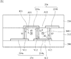
- FIG. 2 is a cross-sectional view schematically illustrating an interconnect structure IS 1 in accordance with various embodiments of the present disclosure.
- the interconnect structure IS 1 includes a substrate 200 , a first insulating layer 212 , a second insulating layer 220 , a first conductive line 214 , a second conductive line 224 , a first conductive via V 11 , a second conductive via V 12 , and a third conductive via V 13 .
- the first insulating layer 212 is disposed on the substrate 200 .
- the substrate 200 may be a semiconductor substrate, such as a bulk semiconductor, a semiconductor-on-insulator (SOI) substrate, or the like.
- SOI semiconductor-on-insulator
- the substrate 200 may be a wafer, such as a silicon wafer.
- An SOI substrate includes a layer of a semiconductor material formed on an insulator layer.
- the semiconductor material of the substrate may include silicon; germanium; a compound semiconductor including silicon carbide, gallium arsenic, gallium phosphide, indium phosphide, indium arsenide, and/or indium antimonide; an alloy semiconductor including SiGe, GaAsP, AlInAs, AlGaAs, GaInAs, GaInP, and/or GaInAsP; or combinations thereof.
- the substrate 200 may include semiconductor elements such as transistors, capacitors, but not limited thereto.
- the second insulating layer 220 is disposed on the first insulating layer 212 .
- the first conductive line 214 is embedded in the first insulating layer 212 and in contact with the substrate 200 , and includes a first portion 214 a and a second portion 214 b .
- the second conductive line 224 is embedded in the second insulating layer 220 and in contact with the first insulating layer 212 , and includes a third portion 224 a and a fourth portion 224 b .
- the first conductive via V 11 , the second conductive via V 12 , and the third conductive via V 13 are embedded in the first insulating layer 212 .
- the first conductive via V 11 connects the first portion 214 a and the third portion 224 a .
- the second conductive via V 12 connects the second portion 214 b and the third portion 224 a .
- the third conductive via V 13 connects the second portion 214 b and the fourth portion 224 b.
- a first cross-sectional area A 11 surrounded by the first portion 214 a , the second portion 214 b , the third portion 224 a , the first conductive via V 11 , and the second conductive via V 12 is substantially equal to a second cross-sectional area A 12 surrounded by the second portion 214 b , the third portion 224 a , the fourth portion 224 b , the second conductive via V 12 , and third conductive via V 13 .
- the first cross-sectional area A 11 is surrounded by the edges of the first portion 214 a , the second portion 214 b , the third portion 224 a , the first conductive via V 11 , the second conductive via V 12 , and the substrate 200
- the second cross-sectional area A 12 is surrounded by the edges of the second portion 214 b , the third portion 224 a , the fourth portion 224 b , the second conductive via V 12 , the third conductive via V 13 , and the second insulating layer 220 .
- the thickness of the first conductive line 214 is much less than the thickness of the first insulating layer 212 . In other words, the first conductive line 214 is relatively thin, and thus its thickness can be ignored.
- the first cross-sectional area A 11 is substantially a height h 1 between the first portion 214 a and the third portion 224 a multiplied by a distance d 1 between the first conductive via V 11 and the second conductive via V 12 . In some embodiments, the first cross-sectional area A 11 is substantially a height h 2 between the second portion 214 b and the third portion 224 a multiplied by the distance d 1 between the first conductive via V 11 and the second conductive via V 12 .
- the second cross-sectional area A 12 is substantially a height h 3 between the second portion 214 b and the fourth portion 224 b multiplied by a distance d 2 between the second conductive via V 12 and the third conductive via V 13 . In some embodiments, the second cross-sectional area A 12 is substantially the height h 2 between the second portion 214 b and the third portion 224 a multiplied by the distance d 2 between the second conductive via V 12 and the third conductive via V 13 .
- the height h 1 between the first portion 214 a and the third portion 224 a is substantially equal to the distance d 1 between the first conductive via V 11 and the second conductive via V 12 .
- the height h 2 between the second portion 214 b and the third portion 224 a is substantially equal to the distance d 1 between the first conductive via V 11 and the second conductive via V 12 .
- the height h 3 between the second portion 214 b and the fourth portion 224 b is substantially equal to the distance d 2 between the second conductive via V 12 and the third conductive via V 13 .
- the height h 2 between the second portion 214 b and the third portion 224 a is substantially equal to the distance d 2 between the second conductive via V 12 and the third conductive via V 13 .
- FIG. 3 schematically illustrates the direction of induced currents when the interconnect structure IS 1 shown in FIG. 2 is in a changing magnetic field MF 1 .
- the interconnect structure IS 1 is disposed in a semiconductor structure, such as chip, and the changing magnetic field MF 1 may generated by a circuit element (such as radio-frequency (RF) circuit).
- RF radio-frequency
- the direction of the changing magnetic field MF 1 is into the plane as shown in FIG. 3 .
- the magnitude and direction of induced currents can be known by Lenz's law, which states that the direction of the current induced in a conductor by a changing magnetic field is such that the magnetic field created by the induced current opposes the initial changing magnetic field, and is shown by the negative sign in Faraday's law of induction:
- ⁇ - ⁇ ⁇ ⁇ B ⁇ ⁇ t which indicates that the induced electromotive force ⁇ and the rate of change in magnetic flux ⁇ B have opposite signs.
- the interconnect structure IS 1 can prevent the noise interference from other circuit element (such as wire).
- FIG. 4 is a cross-sectional view schematically illustrating an interconnect structure IS 2 in accordance with various embodiments of the present disclosure.
- the difference between FIG. 4 and FIG. 2 is that, in the interconnect structure IS 2 , the height h 1 is larger than the distance d 1 , the height h 2 is larger than the distance d 1 , the height h 3 is larger than the distance d 2 , and the height h 2 is larger than the distance d 2 .
- FIG. 5 is a cross-sectional view schematically illustrating an interconnect structure IS 3 in accordance with various embodiments of the present disclosure.
- the difference between FIG. 5 and FIG. 2 is that, in the interconnect structure IS 3 , the height h 1 is smaller than the distance d 1 , the height h 2 is smaller than the distance d 1 , the height h 3 is smaller than the distance d 2 , and the height h 2 is smaller than the distance d 2 .
- FIG. 6 is a cross-sectional view schematically illustrating an interconnect structure in accordance with various embodiments of the present disclosure.
- the interconnect structure IS 4 includes a substrate 200 , a first insulating layer 612 , a second insulating layer 622 , a third insulating layer 632 , a first conductive line 614 , a second conductive line 624 , a third conductive line 634 , a first conductive via V 21 , a second conductive via V 22 , a third conductive via V 23 and a fourth conductive via V 24 .
- the first insulating layer 612 is disposed on the substrate 200 .
- the second insulating layer 622 is disposed on the first insulating layer 612 .
- the third insulating layer 632 is disposed on the second insulating layer 622 .
- the first conductive line 614 is embedded in the first insulating layer 612 and in contact with the substrate 200 .
- the second conductive line 624 is embedded in the second insulating layer 622 and in contact with the first insulating layer 612 , and includes a first portion 624 a , a second portion 624 b , and a third portion 624 c .
- the third conductive line 634 is embedded in the third insulating layer 632 and in contact with the second insulating layer 622 .
- the first conductive via V 21 and the second conductive via V 22 are embedded in the first insulating layer 612 .
- the first conductive via V 21 connects the first conductive line 614 and the first portion 624 a .
- the second conductive via V 22 connects the first conductive line 614 and the second portion 624 b .
- the third conductive via V 23 and the fourth conductive via V 24 are embedded in the second insulating layer 622 .
- the third conductive via V 23 connects the first portion 624 a and the third conductive line 634 .
- the fourth conductive via V 24 connects the third portion 624 c and the third conductive line 634 .
- a first cross-sectional area A 21 surrounded by the first conductive line 614 , the first conductive via V 21 , the second conductive via V 22 , the first portion 624 a , and the second portion 624 b is substantially equal to a second cross-sectional area A 22 surrounded by the first portion 624 a , the third portion 624 c , the third conductive via V 23 , the fourth conductive via V 24 , and the third conductive line 634 .
- the first cross-sectional area A 21 is surrounded by the edges of the first conductive line 614 , the first conductive via V 21 , the second conductive via V 22 , the first portion 624 a , the second portion 624 b , and the second insulating layer 622
- the second cross-sectional area A 22 is surrounded by the edges of the first portion 624 a , the third portion 624 c , the third conductive via V 23 , the fourth conductive via V 24 , the third conductive line 634 , and the first insulating layer 612 .
- the thickness of the second conductive line 624 is much less than the thickness of the second insulating layer 622 . In other words, the second conductive line 624 is relatively thin, and thus its thickness can be ignored.
- the first cross-sectional area A 21 is substantially a height h 4 between the first conductive line 614 and the first portion 624 a multiplied by a distance d 3 between the first conductive via V 21 and the second conductive via V 22 . In some embodiments, the first cross-sectional area A 21 is substantially a height h 5 between the first conductive line 614 and the second portion 624 b multiplied by the distance d 3 between the first conductive via V 21 and the second conductive via V 22 .
- the second cross-sectional area A 22 is substantially a height h 6 between the first portion 624 a and the third conductive line 634 multiplied by a distance d 4 between the third conductive via V 23 and the fourth conductive via V 24 . In some embodiments, the second cross-sectional area A 22 is substantially a height h 7 between the third portion 624 c and the third conductive line 634 multiplied by the distance d 4 between the third conductive via V 23 and the fourth conductive via V 24 .
- the height h 4 between the first conductive line 614 and the first portion 624 a is substantially equal to the distance d 3 between the first conductive via V 21 and the second conductive via V 22
- the height h 5 between the first conductive line 614 and the second portion 624 b is substantially equal to the distance d 3 between the first conductive via V 21 and the second conductive via V 22
- the height h 6 between the first portion 624 a and the third conductive line 634 is substantially equal to the distance d 4 between the third conductive via V 23 and the fourth conductive via V 24
- the height h 7 between the third portion 624 c and the third conductive line 634 is substantially equal to the distance d 4 between the third conductive via V 23 and the fourth conductive via V 24 .
- FIG. 7 schematically illustrates the direction of induced currents when the interconnect structure IS 4 shown in FIG. 6 is in a changing magnetic field MF 2 .
- the interconnect structure IS 4 is disposed in a semiconductor structure, such as chip, and the changing magnetic field MF 2 may generated by a circuit element (such as wire) bonded to the chip.
- the direction of the changing magnetic field MF 2 is into the plane as shown in FIG. 7 .
- the induced current IC 3 can be offset by the induced current IC 4 , and thus the changing magnetic field MF 2 would not influence the operation of the first conductive line 614 , the second conductive line 624 , the third conductive line 634 , the first conductive via V 21 , the second conductive via V 22 , the third conductive via V 23 , and the fourth conductive via V 24 .
- the interconnect structure IS 4 can prevent the noise interference from other circuit element (such as wire).
- FIG. 8 is a cross-sectional view schematically illustrating an interconnect structure IS 5 in accordance with various embodiments of the present disclosure.
- the difference between FIG. 8 and FIG. 6 is that, in the interconnect structure IS 5 , the height between h 4 is smaller than the distance d 3 , and the height h 5 is smaller than the distance d 3 .
- FIG. 9 is a cross-sectional view schematically illustrating an interconnect structure IS 6 in accordance with various embodiments of the present disclosure.
- the difference between FIG. 9 and FIG. 6 is that, in the interconnect structure IS 6 , the height between h 4 is larger than the distance d 3 , and the height h 5 is larger than the distance d 3 .
- FIG. 10 is a cross-sectional view schematically illustrating an interconnect structure IS 7 in accordance with various embodiments of the present disclosure.
- the difference between FIG. 10 and FIG. 6 is that, in the interconnect structure IS 7 , the height h 6 is smaller than the distance d 4 , and the height h 7 is smaller than the distance d 4 .
- FIG. 11 is a cross-sectional view schematically illustrating an interconnect structure IS 8 in accordance with various embodiments of the present disclosure.
- the difference between FIG. 11 and FIG. 6 is that, in the interconnect structure IS 8 , the height h 6 is larger than the distance d 4 , and the height h 7 is larger than the distance d 4 .
- FIG. 12 is a cross-sectional view schematically illustrating an interconnect structure IS 9 in accordance with various embodiments of the present disclosure.
- the difference between FIG. 12 and FIG. 6 is that, in the interconnect structure IS 9 , the height between h 4 is smaller than the distance d 3 , the height h 5 is smaller than the distance d 3 , the height h 6 is larger than the distance d 4 , and the height h 7 is larger than the distance d 4 .
- FIG. 13 is a cross-sectional view schematically illustrating an interconnect structure IS 10 in accordance with various embodiments of the present disclosure.
- the difference between FIG. 13 and FIG. 6 is that, in the interconnect structure IS 10 , the height between h 4 is larger than the distance d 3 , the height h 5 is larger than the distance d 3 , the height h 6 is smaller than the distance d 4 , and the height h 7 is smaller than the distance d 4 .
Landscapes
- Internal Circuitry In Semiconductor Integrated Circuit Devices (AREA)
- Physics & Mathematics (AREA)
- Health & Medical Sciences (AREA)
- Electromagnetism (AREA)
- Toxicology (AREA)
- Design And Manufacture Of Integrated Circuits (AREA)
Abstract
Description
which indicates that the induced electromotive force ε and the rate of change in magnetic flux ϕB have opposite signs. The magnetic flux is shown by the following formula:
ΦB =∫B·dA,
in which B represents a magnetic field, and A represents an area perpendicular to the magnetic field. Therefore, according to Lenz's law, it can be known that the direction of an induced current IC1 flowing through the first conductive via V11, second conductive via V12, and
Claims (9)
Priority Applications (3)
| Application Number | Priority Date | Filing Date | Title |
|---|---|---|---|
| US17/105,480 US11404384B2 (en) | 2019-08-19 | 2020-11-25 | Interconnect structure |
| US17/808,300 US12033956B2 (en) | 2019-08-19 | 2022-06-22 | Interconnect structure |
| US18/673,298 US20240312929A1 (en) | 2019-08-19 | 2024-05-23 | Interconnect structure |
Applications Claiming Priority (2)
| Application Number | Priority Date | Filing Date | Title |
|---|---|---|---|
| US16/544,887 US10886236B1 (en) | 2019-08-19 | 2019-08-19 | Interconnect structure |
| US17/105,480 US11404384B2 (en) | 2019-08-19 | 2020-11-25 | Interconnect structure |
Related Parent Applications (1)
| Application Number | Title | Priority Date | Filing Date |
|---|---|---|---|
| US16/544,887 Division US10886236B1 (en) | 2019-08-19 | 2019-08-19 | Interconnect structure |
Related Child Applications (1)
| Application Number | Title | Priority Date | Filing Date |
|---|---|---|---|
| US17/808,300 Division US12033956B2 (en) | 2019-08-19 | 2022-06-22 | Interconnect structure |
Publications (2)
| Publication Number | Publication Date |
|---|---|
| US20210082834A1 US20210082834A1 (en) | 2021-03-18 |
| US11404384B2 true US11404384B2 (en) | 2022-08-02 |
Family
ID=74045325
Family Applications (4)
| Application Number | Title | Priority Date | Filing Date |
|---|---|---|---|
| US16/544,887 Active US10886236B1 (en) | 2019-08-19 | 2019-08-19 | Interconnect structure |
| US17/105,480 Active 2039-09-02 US11404384B2 (en) | 2019-08-19 | 2020-11-25 | Interconnect structure |
| US17/808,300 Active 2039-08-19 US12033956B2 (en) | 2019-08-19 | 2022-06-22 | Interconnect structure |
| US18/673,298 Pending US20240312929A1 (en) | 2019-08-19 | 2024-05-23 | Interconnect structure |
Family Applications Before (1)
| Application Number | Title | Priority Date | Filing Date |
|---|---|---|---|
| US16/544,887 Active US10886236B1 (en) | 2019-08-19 | 2019-08-19 | Interconnect structure |
Family Applications After (2)
| Application Number | Title | Priority Date | Filing Date |
|---|---|---|---|
| US17/808,300 Active 2039-08-19 US12033956B2 (en) | 2019-08-19 | 2022-06-22 | Interconnect structure |
| US18/673,298 Pending US20240312929A1 (en) | 2019-08-19 | 2024-05-23 | Interconnect structure |
Country Status (3)
| Country | Link |
|---|---|
| US (4) | US10886236B1 (en) |
| CN (1) | CN112397480B (en) |
| TW (1) | TWI708357B (en) |
Citations (5)
| Publication number | Priority date | Publication date | Assignee | Title |
|---|---|---|---|---|
| US6492716B1 (en) | 2001-04-30 | 2002-12-10 | Zeevo, Inc. | Seal ring structure for IC containing integrated digital/RF/analog circuits and functions |
| US20150076665A1 (en) * | 2013-09-18 | 2015-03-19 | United Microelectronics Corp. | Alignment mark structure |
| US20170019990A1 (en) * | 2014-03-31 | 2017-01-19 | Murata Manufacturing Co., Ltd. | Multilayer circuit board and probe card including the same |
| US9865482B2 (en) | 2008-09-09 | 2018-01-09 | STATS ChipPAC Pte. Ltd. | Semiconductor device and method of forming a fan-out structure with integrated passive device and discrete component |
| US20180061463A1 (en) * | 2016-08-29 | 2018-03-01 | Samsung Electronics Co., Ltd. | Pre-charge circuit for preventing inrush current and electronic device including the same |
Family Cites Families (7)
| Publication number | Priority date | Publication date | Assignee | Title |
|---|---|---|---|---|
| US7456507B2 (en) * | 2006-01-12 | 2008-11-25 | Taiwan Semiconductor Manufacturing Co., Ltd. | Die seal structure for reducing stress induced during die saw process |
| US7812426B2 (en) * | 2008-05-30 | 2010-10-12 | Taiwan Semiconductor Manufacturing Company, Ltd. | TSV-enabled twisted pair |
| US8736065B2 (en) * | 2010-12-22 | 2014-05-27 | Intel Corporation | Multi-chip package having a substrate with a plurality of vertically embedded die and a process of forming the same |
| US8648592B2 (en) * | 2011-09-13 | 2014-02-11 | Taiwan Semiconductor Manufacturing Company, Ltd. | Semiconductor device components and methods |
| US9881894B2 (en) * | 2012-03-08 | 2018-01-30 | STATS ChipPAC Pte. Ltd. | Thin 3D fan-out embedded wafer level package (EWLB) for application processor and memory integration |
| US9299656B2 (en) * | 2014-06-02 | 2016-03-29 | Infineon Technologies Ag | Vias and methods of formation thereof |
| US9947683B2 (en) * | 2015-09-11 | 2018-04-17 | Toshiba Memory Corporation | Three-dimensional semiconductor memory device and method for manufacturing the same |
-
2019
- 2019-08-19 US US16/544,887 patent/US10886236B1/en active Active
- 2019-10-21 TW TW108137935A patent/TWI708357B/en active
- 2019-10-25 CN CN201911025768.3A patent/CN112397480B/en active Active
-
2020
- 2020-11-25 US US17/105,480 patent/US11404384B2/en active Active
-
2022
- 2022-06-22 US US17/808,300 patent/US12033956B2/en active Active
-
2024
- 2024-05-23 US US18/673,298 patent/US20240312929A1/en active Pending
Patent Citations (5)
| Publication number | Priority date | Publication date | Assignee | Title |
|---|---|---|---|---|
| US6492716B1 (en) | 2001-04-30 | 2002-12-10 | Zeevo, Inc. | Seal ring structure for IC containing integrated digital/RF/analog circuits and functions |
| US9865482B2 (en) | 2008-09-09 | 2018-01-09 | STATS ChipPAC Pte. Ltd. | Semiconductor device and method of forming a fan-out structure with integrated passive device and discrete component |
| US20150076665A1 (en) * | 2013-09-18 | 2015-03-19 | United Microelectronics Corp. | Alignment mark structure |
| US20170019990A1 (en) * | 2014-03-31 | 2017-01-19 | Murata Manufacturing Co., Ltd. | Multilayer circuit board and probe card including the same |
| US20180061463A1 (en) * | 2016-08-29 | 2018-03-01 | Samsung Electronics Co., Ltd. | Pre-charge circuit for preventing inrush current and electronic device including the same |
Also Published As
| Publication number | Publication date |
|---|---|
| TW202109813A (en) | 2021-03-01 |
| US10886236B1 (en) | 2021-01-05 |
| CN112397480A (en) | 2021-02-23 |
| CN112397480B (en) | 2024-06-18 |
| US20220320009A1 (en) | 2022-10-06 |
| US20240312929A1 (en) | 2024-09-19 |
| US20210082834A1 (en) | 2021-03-18 |
| US12033956B2 (en) | 2024-07-09 |
| TWI708357B (en) | 2020-10-21 |
Similar Documents
| Publication | Publication Date | Title |
|---|---|---|
| US8093670B2 (en) | Methods and apparatus for integrated circuit having on chip capacitor with eddy current reductions | |
| CN112424929A (en) | Heat extraction for single layer transfer integrated circuits | |
| US11424228B2 (en) | Semiconductor structure and method for manufacturing the same | |
| US6404026B2 (en) | Semiconductor devices | |
| US20220149036A1 (en) | Die backend diodes for electrostatic discharge (esd) protection | |
| US6396123B1 (en) | Semiconductor device provided with on-chip decoupling condenser utilizing CMP dummy patterns | |
| US11387316B2 (en) | Monolithic back-to-back isolation elements with floating top plate | |
| US11404384B2 (en) | Interconnect structure | |
| US11736134B2 (en) | Digital isolator | |
| US7936071B2 (en) | Semiconductor device having a specified terminal layout pattern | |
| US11605627B2 (en) | Systems and methods for protecting a semiconductor device | |
| US20130020673A1 (en) | Protection diode and semiconductor device having the same | |
| US20120220101A1 (en) | Internal conductive layer | |
| CN112310046B (en) | Semiconductor structure and method for manufacturing the same | |
| US6727578B1 (en) | Semiconductor device having power supply voltage routed through substrate | |
| US8415802B2 (en) | Strip conductor structure for minimizing thermomechanical loads | |
| US6975136B2 (en) | Isolated channel in an integrated circuit | |
| CN120388937A (en) | Semiconductor structure and method for forming semiconductor structure | |
| CN114171494A (en) | Diode and semiconductor structure thereof | |
| JPS604265A (en) | Insulated gate type field effect semiconductor device | |
| JP3189797B2 (en) | Manufacturing method of semiconductor integrated circuit | |
| JPH0982885A (en) | Semiconductor device | |
| JPS6120359A (en) | Semiconductor device | |
| KR19980084130A (en) | Semiconductor device with electromagnetic shielding and manufacturing method |
Legal Events
| Date | Code | Title | Description |
|---|---|---|---|
| AS | Assignment |
Owner name: NANYA TECHNOLOGY CORPORATION, TAIWAN Free format text: ASSIGNMENT OF ASSIGNORS INTEREST;ASSIGNORS:KANG, TING-CIH;CHIU, HSIH-YANG;REEL/FRAME:054473/0929 Effective date: 20190731 |
|
| FEPP | Fee payment procedure |
Free format text: ENTITY STATUS SET TO UNDISCOUNTED (ORIGINAL EVENT CODE: BIG.); ENTITY STATUS OF PATENT OWNER: LARGE ENTITY |
|
| STPP | Information on status: patent application and granting procedure in general |
Free format text: APPLICATION DISPATCHED FROM PREEXAM, NOT YET DOCKETED |
|
| STPP | Information on status: patent application and granting procedure in general |
Free format text: DOCKETED NEW CASE - READY FOR EXAMINATION |
|
| STPP | Information on status: patent application and granting procedure in general |
Free format text: NON FINAL ACTION MAILED |
|
| STPP | Information on status: patent application and granting procedure in general |
Free format text: RESPONSE TO NON-FINAL OFFICE ACTION ENTERED AND FORWARDED TO EXAMINER |
|
| STPP | Information on status: patent application and granting procedure in general |
Free format text: NOTICE OF ALLOWANCE MAILED -- APPLICATION RECEIVED IN OFFICE OF PUBLICATIONS |
|
| STCF | Information on status: patent grant |
Free format text: PATENTED CASE |
|
| MAFP | Maintenance fee payment |
Free format text: PAYMENT OF MAINTENANCE FEE, 4TH YEAR, LARGE ENTITY (ORIGINAL EVENT CODE: M1551); ENTITY STATUS OF PATENT OWNER: LARGE ENTITY Year of fee payment: 4 |