US11383515B2 - Element substrate, liquid discharge head, and printing apparatus - Google Patents
Element substrate, liquid discharge head, and printing apparatus Download PDFInfo
- Publication number
- US11383515B2 US11383515B2 US16/848,983 US202016848983A US11383515B2 US 11383515 B2 US11383515 B2 US 11383515B2 US 202016848983 A US202016848983 A US 202016848983A US 11383515 B2 US11383515 B2 US 11383515B2
- Authority
- US
- United States
- Prior art keywords
- wiring layer
- wiring
- layer
- metal plug
- element substrate
- Prior art date
- Legal status (The legal status is an assumption and is not a legal conclusion. Google has not performed a legal analysis and makes no representation as to the accuracy of the status listed.)
- Active
Links
Images


Classifications
-
- B—PERFORMING OPERATIONS; TRANSPORTING
- B41—PRINTING; LINING MACHINES; TYPEWRITERS; STAMPS
- B41J—TYPEWRITERS; SELECTIVE PRINTING MECHANISMS, i.e. MECHANISMS PRINTING OTHERWISE THAN FROM A FORME; CORRECTION OF TYPOGRAPHICAL ERRORS
- B41J2/00—Typewriters or selective printing mechanisms characterised by the printing or marking process for which they are designed
- B41J2/005—Typewriters or selective printing mechanisms characterised by the printing or marking process for which they are designed characterised by bringing liquid or particles selectively into contact with a printing material
- B41J2/01—Ink jet
- B41J2/135—Nozzles
- B41J2/14—Structure thereof only for on-demand ink jet heads
- B41J2/14016—Structure of bubble jet print heads
- B41J2/14088—Structure of heating means
- B41J2/14112—Resistive element
- B41J2/14129—Layer structure
-
- B—PERFORMING OPERATIONS; TRANSPORTING
- B41—PRINTING; LINING MACHINES; TYPEWRITERS; STAMPS
- B41J—TYPEWRITERS; SELECTIVE PRINTING MECHANISMS, i.e. MECHANISMS PRINTING OTHERWISE THAN FROM A FORME; CORRECTION OF TYPOGRAPHICAL ERRORS
- B41J2/00—Typewriters or selective printing mechanisms characterised by the printing or marking process for which they are designed
- B41J2/005—Typewriters or selective printing mechanisms characterised by the printing or marking process for which they are designed characterised by bringing liquid or particles selectively into contact with a printing material
- B41J2/01—Ink jet
- B41J2/015—Ink jet characterised by the jet generation process
- B41J2/04—Ink jet characterised by the jet generation process generating single droplets or particles on demand
- B41J2/045—Ink jet characterised by the jet generation process generating single droplets or particles on demand by pressure, e.g. electromechanical transducers
- B41J2/04501—Control methods or devices therefor, e.g. driver circuits, control circuits
- B41J2/0458—Control methods or devices therefor, e.g. driver circuits, control circuits controlling heads based on heating elements forming bubbles
-
- B—PERFORMING OPERATIONS; TRANSPORTING
- B41—PRINTING; LINING MACHINES; TYPEWRITERS; STAMPS
- B41J—TYPEWRITERS; SELECTIVE PRINTING MECHANISMS, i.e. MECHANISMS PRINTING OTHERWISE THAN FROM A FORME; CORRECTION OF TYPOGRAPHICAL ERRORS
- B41J2/00—Typewriters or selective printing mechanisms characterised by the printing or marking process for which they are designed
- B41J2/005—Typewriters or selective printing mechanisms characterised by the printing or marking process for which they are designed characterised by bringing liquid or particles selectively into contact with a printing material
- B41J2/01—Ink jet
- B41J2/135—Nozzles
- B41J2/14—Structure thereof only for on-demand ink jet heads
- B41J2/14016—Structure of bubble jet print heads
- B41J2/14072—Electrical connections, e.g. details on electrodes, connecting the chip to the outside...
-
- B—PERFORMING OPERATIONS; TRANSPORTING
- B41—PRINTING; LINING MACHINES; TYPEWRITERS; STAMPS
- B41J—TYPEWRITERS; SELECTIVE PRINTING MECHANISMS, i.e. MECHANISMS PRINTING OTHERWISE THAN FROM A FORME; CORRECTION OF TYPOGRAPHICAL ERRORS
- B41J2/00—Typewriters or selective printing mechanisms characterised by the printing or marking process for which they are designed
- B41J2/005—Typewriters or selective printing mechanisms characterised by the printing or marking process for which they are designed characterised by bringing liquid or particles selectively into contact with a printing material
- B41J2/01—Ink jet
- B41J2/135—Nozzles
- B41J2/14—Structure thereof only for on-demand ink jet heads
- B41J2/14016—Structure of bubble jet print heads
- B41J2/1408—Structure dealing with thermal variations, e.g. cooling device, thermal coefficients of materials
-
- B—PERFORMING OPERATIONS; TRANSPORTING
- B41—PRINTING; LINING MACHINES; TYPEWRITERS; STAMPS
- B41J—TYPEWRITERS; SELECTIVE PRINTING MECHANISMS, i.e. MECHANISMS PRINTING OTHERWISE THAN FROM A FORME; CORRECTION OF TYPOGRAPHICAL ERRORS
- B41J2/00—Typewriters or selective printing mechanisms characterised by the printing or marking process for which they are designed
- B41J2/005—Typewriters or selective printing mechanisms characterised by the printing or marking process for which they are designed characterised by bringing liquid or particles selectively into contact with a printing material
- B41J2/01—Ink jet
- B41J2/135—Nozzles
- B41J2/14—Structure thereof only for on-demand ink jet heads
- B41J2/14016—Structure of bubble jet print heads
- B41J2/14088—Structure of heating means
-
- B—PERFORMING OPERATIONS; TRANSPORTING
- B41—PRINTING; LINING MACHINES; TYPEWRITERS; STAMPS
- B41J—TYPEWRITERS; SELECTIVE PRINTING MECHANISMS, i.e. MECHANISMS PRINTING OTHERWISE THAN FROM A FORME; CORRECTION OF TYPOGRAPHICAL ERRORS
- B41J2/00—Typewriters or selective printing mechanisms characterised by the printing or marking process for which they are designed
- B41J2/005—Typewriters or selective printing mechanisms characterised by the printing or marking process for which they are designed characterised by bringing liquid or particles selectively into contact with a printing material
- B41J2/01—Ink jet
- B41J2/135—Nozzles
- B41J2/14—Structure thereof only for on-demand ink jet heads
- B41J2/14016—Structure of bubble jet print heads
- B41J2/14153—Structures including a sensor
-
- B—PERFORMING OPERATIONS; TRANSPORTING
- B41—PRINTING; LINING MACHINES; TYPEWRITERS; STAMPS
- B41J—TYPEWRITERS; SELECTIVE PRINTING MECHANISMS, i.e. MECHANISMS PRINTING OTHERWISE THAN FROM A FORME; CORRECTION OF TYPOGRAPHICAL ERRORS
- B41J2202/00—Embodiments of or processes related to ink-jet or thermal heads
- B41J2202/01—Embodiments of or processes related to ink-jet heads
- B41J2202/11—Embodiments of or processes related to ink-jet heads characterised by specific geometrical characteristics
-
- B—PERFORMING OPERATIONS; TRANSPORTING
- B41—PRINTING; LINING MACHINES; TYPEWRITERS; STAMPS
- B41J—TYPEWRITERS; SELECTIVE PRINTING MECHANISMS, i.e. MECHANISMS PRINTING OTHERWISE THAN FROM A FORME; CORRECTION OF TYPOGRAPHICAL ERRORS
- B41J2202/00—Embodiments of or processes related to ink-jet or thermal heads
- B41J2202/01—Embodiments of or processes related to ink-jet heads
- B41J2202/13—Heads having an integrated circuit
-
- B—PERFORMING OPERATIONS; TRANSPORTING
- B41—PRINTING; LINING MACHINES; TYPEWRITERS; STAMPS
- B41J—TYPEWRITERS; SELECTIVE PRINTING MECHANISMS, i.e. MECHANISMS PRINTING OTHERWISE THAN FROM A FORME; CORRECTION OF TYPOGRAPHICAL ERRORS
- B41J2202/00—Embodiments of or processes related to ink-jet or thermal heads
- B41J2202/01—Embodiments of or processes related to ink-jet heads
- B41J2202/18—Electrical connection established using vias
Definitions
- an inkjet printing method using a thermal method is a method of locally heating a liquid such as ink to generate bubbles in a nozzle, and discharging the ink from the nozzle by the bubbles and making the ink fly and land on a printed target.
- electrothermal transducers configured to heat ink are integrated on a semiconductor substrate integrally with a logic circuit configured to drive the electrothermal transducers.
- the electrothermal transducers are densely arranged, thereby implementing high-speed driving.
- Japanese Patent Laid-Open No. 2016-137705 describes a method of providing an element substrate aiming at reducing the film thickness of an electrothermal transducer (heater) protective film while ensuring printing performance of high image quality and the performance of the protective film in a printhead according to the thermal method.
- the element substrate includes an electrothermal transducer, an electric wiring layer provided in an insulation film and configured to supply a current to the electrothermal transducer, and a connecting member such as a plug that connects the electric wiring layer and the electrothermal transducer.
- the electrothermal transducer is formed such that the current flows in the first direction (X), the electrothermal transducer includes a connection region to which at least one connecting member is connected, and the connection region extends along the second direction (Y) crossing the first direction (X).
- the dimensional accuracy of formation of an electrode to be connected to the electrothermal transducer can be increased, and the film thickness of the protective film can be reduced by suppressing a step difference under the protective film.
- the film thickness of the protective film is reduced, if an unexpected pinhole is formed in the protective film, a liquid such as ink may enter from that portion into the element region of the protective film. This increases the possibility that an electrothermal transducer, an electric connecting member, an electric wiring, or the like comes into contact with the liquid. As described above, device reliability may lower along with the reduction of the film thickness of the protective film.
- the ink may enter to below the protective film so that an electrothermal transducer, a plug that is an electric connecting member, a conductive film such as an electric wiring, and an insulation film may dissolve into the ink, and corrosion may progress.
- wiring corrosion derived from a certain electrothermal transducer greatly progresses, and the corrosion reaches a wiring portion connected to an electrothermal transducer on the periphery, driving may be unstable not only in the electrothermal transducer as the starting point of the corrosion but also in the electrothermal transducer on the periphery, and normal driving may be impossible.
- a high potential may be applied to an electrode pair or wiring connected to drive the electrothermal transducer.
- a so-called electric corrosion action that is, progress of an anode reaction on an ink contact interface increases the progress speed of corrosion in a metallic film that is a wiring material.
- a countermeasure to suppress or prevent the progress of corrosion needs to be taken.
- the present invention is conceived as a response to the above-described disadvantages of the conventional art.
- an element substrate, a liquid discharge head, and a printing apparatus according to this invention are capable of suppressing spread of electric corrosion of a wiring connected to a heater.
- a multilayer structured element substrate including a heater layer in which a plurality of heaters configured to discharge a liquid are formed, and a first wiring layer in which a common wiring configured to supply a voltage from an outside to the plurality of heaters is formed, comprising: a second wiring layer formed between the heater layer and the first wiring layer in a lamination direction and made of a high anticorrosion material to the discharged liquid as compared to the first wiring layer; a first metal plug that is in contact with a surface of the second wiring layer on a side of the heater layer, and fills an interior of a first through-hole elongated to the side of the heater layer; and a second metal plug that is in contact with a surface of the second wiring layer on a side of the first wiring layer in a place different from a place where the first through-hole is formed when the element substrate is viewed in a planar view, and fills an interior of a second through-hole elongated to the side of the first wiring layer
- a liquid discharge head using the above described multilayer structured element substrate comprising a plurality of orifices configured to discharge a liquid.
- a printing apparatus for performing printing on a print medium using the above described liquid discharge head configured to discharge a liquid as a printhead configured to discharge ink as the liquid, wherein the plurality of heaters are in contact with the ink, and the ink is discharged from the orifices by driving the plurality of heaters.
- the invention is particularly advantageous since it is possible to suppress spread of corrosion of a wiring connected to a heater. This can suppress the influence of progress of wiring corrosion on heaters on the periphery and maintain the operation reliability of the element substrate.
- FIG. 1 is a perspective view showing the schematic arrangement of a printing apparatus including a printhead according to an exemplary embodiment of the present invention
- FIG. 2 is a block diagram showing the control configuration of the printing apparatus shown in FIG. 1 ;
- FIGS. 3A and 3B are views showing the layout arrangement of an element substrate (head substrate) integrated on a printhead;
- FIG. 4 is a view showing an equivalent circuit of a driving circuit configured to drive one heater
- FIG. 6 is a sectional view showing a state in which corrosion of an electric wiring of the element substrate has progressed
- FIGS. 7A and 7B are plan views showing the schematic arrangement of the vicinity of heaters 101 on the element substrate
- FIG. 8 is a sectional view showing the multilayer structure of an element substrate according to the first embodiment
- FIG. 9 is a sectional view showing the multilayer structure of an element substrate according to the second embodiment.
- FIG. 10 is a sectional view showing the multilayer structure of an element substrate according to the third embodiment.
- FIG. 12 is a plan view showing the state of the wirings of two heaters integrated on the element substrate shown in FIG. 11 .
- the term “print medium” not only includes a paper sheet used in common printing apparatuses, but also broadly includes materials, such as cloth, a plastic film, a metal plate, glass, ceramics, wood, and leather, capable of accepting ink.
- a “nozzle” (to be also referred to as “print element” hereinafter) generically means an ink orifice or a liquid channel communicating with it, and an element for generating energy used to discharge ink, unless otherwise specified.
- An element substrate for a printhead (head substrate) used below means not merely a base made of a silicon semiconductor, but an arrangement in which elements, wirings, and the like are arranged.
- “on the substrate” means not merely “on an element substrate”, but even “the surface of the element substrate” and “inside the element substrate near the surface”.
- “built-in” means not merely arranging respective elements as separate members on the base surface, but integrally forming and manufacturing respective elements on an element substrate by a semiconductor circuit manufacturing process or the like.
- an ink tank 6 storing ink to be supplied to the printhead 3 is attached to the carriage 2 of the printing apparatus 1 .
- the ink tank 6 is detachable from the carriage 2 .
- a printing apparatus 1 shown in FIG. 1 can perform color printing, and for the purpose, four ink cartridges storing magenta (M), cyan (C), yellow (Y), and black (K) inks, respectively, are mounted on the carriage 2 .
- the four ink cartridges are detachable independently.
- the printhead 3 employs an inkjet method of discharging ink using thermal energy.
- the printhead 3 includes an electrothermal transducer (heater).
- the electrothermal transducer is provided in correspondence with each orifice.
- a pulse voltage is applied to a corresponding electrothermal transducer in accordance with a print signal, thereby discharging ink from a corresponding orifice.
- the printing apparatus is not limited to the above-described serial type printing apparatus, and the embodiment can also be applied to a so-called full line type printing apparatus in which a printhead (line head) with orifices arrayed in the widthwise direction of a print medium is arranged in the conveyance direction of the print medium.
- FIG. 2 is a block diagram showing the control configuration of the printing apparatus shown in FIG. 1 .
- a controller 600 is formed by an MPU 601 , a ROM 602 , an application specific integrated circuit (ASIC) 603 , a RAM 604 , a system bus 605 , an A/D converter 606 , and the like.
- the ROM 602 stores programs corresponding to control sequences to be described later, necessary tables, and other fixed data.
- the ASIC 603 generates control signals for control of a carriage motor M 1 , control of a conveyance motor M 2 , and control of the printhead 3 .
- the RAM 604 is used as an image data expansion area, a working area for program execution, and the like.
- the system bus 605 connects the MPU 601 , the ASIC 603 , and the RAM 604 to each other to exchange data.
- the A/D converter 606 receives an analog signal from a sensor group to be described below, performs A/D conversion, and supplies a digital signal to the MPU 601 .
- Reference numeral 620 denotes a switch group which is formed by a power switch 621 , a print switch 622 , a recovery switch 623 , and the like.
- Reference numeral 630 denotes a sensor group configured to detect an apparatus state and formed by a position sensor 631 , a temperature sensor 632 , and the like.
- Reference numeral 640 denotes a carriage motor driver that drives the carriage motor M 1 configured to reciprocally scan the carriage 2 in the direction of the arrow A; and 642 , a conveyance motor driver that drives the conveyance motor M 2 configured to convey the print medium P.
- the ASIC 603 transfers data used to drive a heating element (a heater for ink discharge) to the printhead while directly accessing the storage area of the RAM 604 at the time of print scan by the printhead 3 .
- the printing apparatus includes a display unit formed by an LCD or an LED as a user interface.
- FIGS. 3A and 3B are plan views showing the layout arrangement of an element substrate 700 integrated on the printhead 3 .
- the plane of the element substrate 700 shown in FIG. 3A has a rectangular shape.
- a plurality of pads 201 are provided along the long side of the rectangular plane of the element substrate 700 , and data and a driving voltage are supplied from the outside (the main body portion of the printing apparatus) via the pads.
- a plurality of heaters 101 , a plurality of orifices 109 , a plurality of ink supply ports 203 , and a plurality of switching elements 300 are arrayed in the long side direction of the element substrate 700 .
- FIG. 3A In the example shown in FIG. 3A , four heater arrays, four orifice arrays, eight ink supply port arrays, and four switching element arrays are provided.
- the ink supply port arrays are formed on both sides of each of the four heater arrays.
- Magenta (M), cyan (C), yellow (Y), and black (K) inks are supplied to the four ink supply port arrays, respectively.
- FIG. 3B is an enlarged view of a portion A shown in FIG. 3A .
- the orifice 109 that discharges ink droplets is provided in correspondence with each heater 101 , and the switching elements 300 that drive the heaters are provided on both sides of the orifices.
- the array pitch of the heaters is 1 ⁇ 2 of the array pitch of the switching elements.
- FIG. 4 is a view showing an equivalent circuit of a driving circuit configured to drive one heater.
- a connecting portion 341 on one side of the heater (electrothermal transducer) 101 is electrically connected to a VH common wiring 131 used to supply a voltage.
- the other connecting portion 342 of the heater 101 is electrically connected to a GND common wiring 141 via the switching element 300 (driver) configured to switch ON/OFF of driving of the heater 101 .
- the switching element 300 is a MOSFET. A driving voltage from the outside is applied to the gate of the MOSFET to switch ON/OFF and drive the heater 101 .
- an element substrate having a conventional arrangement will be described first as a comparative example, and then, the features of an element substrate according to this embodiment will be described.
- FIGS. 5A and 5B are sectional views showing the multilayer structure of an element substrate as a comparative example.
- FIG. 5A is a sectional view taken along a line A-A′ shown in FIG. 3B
- FIG. 5B is a sectional view taken along a line B-B′ shown in FIG. 3B .
- the electric wirings are thus configured as four layers whose distances from the heater (electrothermal transducer) 101 are different from each other.
- a protective film 105 configured to prevent the heater from directly coming into contact with ink is formed.
- the protective film 105 is an insulation layer configured to insulate the heater 101 and the anti-cavitation layer 106 from each other.
- An orifice 109 is formed by a hole in a top plate 108 that covers an element substrate 700 .
- the electric wiring layers will be defined as the first wiring layer 103 a , the second wiring layer 103 b , the third wiring layer 103 c , and the fourth wiring layer 103 d from the lower layer side.
- the first wiring layer 103 a and the second wiring layer 103 b on the side close to the Si substrate 113 of the lower layer are assigned to a signal wiring layer and a logic power supply wiring layer used to drive the heater 101 .
- the third wiring layer 103 c and the fourth wiring layer 103 d on the upper layer side are assigned to wiring layers used to supply a current to the heater 101 .
- the wiring layers 103 a to 103 d are made of, for example, aluminum or an alloy (for example, AlSi or AlCu) containing aluminum.
- a GND wiring is formed in the fourth wiring layer 103 d
- a VH power supply wiring is formed in the third wiring layer 103 c .
- Both the VH power supply wiring and the GND wiring are common wirings to a plurality of heaters, and will therefore also be referred to as a VH power supply common wiring and a GND common wiring hereinafter.
- the VH power is supplied from the outside (the main body portion of the printing apparatus) of the printhead.
- the wiring layers of the upper layers and the lower layers are connected by metal plugs (connecting members) 100 b and 102 a to 102 d formed in through-holes formed to penetrate the insulation layers 100 a and 104 a to 104 d , respectively.
- a barrier metal formed by a titanium nitride (TiN) film or the like is formed on the lower surface and the side surface of each through-hole, and the lower surface side and the side surface side of the metal plug are surrounded by the barrier metal.
- the four wiring layers 103 a to 103 d will generically be referred to as wiring layers 103
- the four metal plugs 102 a to 102 d will generically be referred to as connecting members 102 .
- FIG. 6 is a sectional view taken along a line B-B′ shown in FIG. 3B in a case in which corrosion of an electric wiring of the element substrate has progressed. Note that the same reference numerals as already described with reference to FIGS. 5A and 5B denote similar constituent elements in FIG. 6 , and a description thereof will be omitted.
- FIG. 6 schematically shows a state in which corrosion of the metal plugs 102 d and 102 c and the wiring of the wiring layer 103 c has progressed up to the VH power supply common wiring.
- the VH power supply common wiring formed in the third wiring layer 103 c is configured to feed power to an adjacent heater as well. For this reason, if the wiring corrosion progresses more widely, power feeding to peripheral heaters cannot be performed, and an ink discharge failure may occur.
- a pinhole or the like is formed in the protective film 105 , and ink (liquid) enters from it to cause corrosion, as described above.
- FIGS. 7A and 7B are plan views showing the schematic arrangement of the vicinity of the heaters 101 on the element substrate.
- each heater 101 is connected to the VH power supply common wiring formed in the wiring layer 103 c via the metal plug 102 d that fills the through-hole.
- the other terminal of each heater 101 is connected to the switching element 300 formed in the lowermost layer via the metal plug 102 d that fills the through-hole.
- the switching element 300 is connected to the GND common wiring formed in the wiring layer 103 d.
- the first type is a metal that does not corrode in itself, or a metal that has stability and hardly corrodes.
- Most metallic corrosions are electrochemical reactions that occur due to a potential difference on the surface.
- an anode reaction occurs on a metal surface, and the metal dissolves as metal ions, metallic corrosion progresses.
- the easiness of dissolution and the easiness of ionization are represented by an ionization tendency.
- the second type is a metal that hardly corrodes when a passivation film is formed on the surface.
- a metal of this type a very thin film called a passivation film is formed on the surface, and this prevents corrosion from progressing.
- the passivation film immediately reacts with oxygen or the like to do self-repairing.
- the strength of the passivation film and what readily breaks the passivation film are different depending on the metal. Titanium, tantalum, zirconium, niobium, and the like correspond to metals of this type.
- the third type is a metal for which a corroded product is formed on the surface, and which functions as a protective film.
- the corroded products of some metals corrode the metals to tatters, and the corroded products of some metals prevent progress of corrosion to some extent and function like a protective film when formed on a surface.
- the corroded product may directly act as a protective film. Examples are copper, zinc, and lead.
- the potential-ph diagram is a state diagram showing the regions of a potential and a ph in which metals, metal ions, and metal compounds can stably exist at a predetermined temperature. More specifically, in the potential-ph diagram, the existing region of a chemical species (particularly a metal) in water is shown as the stable existence range of the chemical species on two-dimensional coordinates by plotting an electrode potential corresponding to the oxidizing power of a solution along the ordinate and ph along the abscissa. It is possible to read, from the potential-ph diagram, whether a specific oxide or complex ions are generated at a specific potential and ph of a given metal or whether a reaction does not occur.
- Titanium nitride that is a nitride of titanium is a material widely used as a barrier metal or an antireflection film in general, and is also a very hard ceramic material, and has a corrosion resistance. For this reason, this material is used as a coating to a cutting tool such as a cutter. Titanium is ionized and dissolved in an environment of a liquid with an acidic ph and a negative potential. In a neutral or alkaline ph environment of a general print ink, since titanium takes an oxidation region independently of its potential, it can be read that the titanium does not dissolve. Since titanium has such a characteristic, titanium nitride that is a nitride of titanium is also considered to have a corrosion resistance.
- the general corrosion resistance of a metal has been described above.
- the detailed material is merely an example.
- the progress speed of corrosion is different depending on the temperature environment, the potential of the target metal, and an electrolyte to which the metal is exposed.
- the corrosion resistances of various kinds of metals change depending on the influence of the peripheral environment.
- a metal nitride such as titanium nitride (TiN) or tantalum nitride (TaN) is a material generally used as a barrier metal in a semiconductor manufacturing process. Since the conductive film can readily be incorporated in the manufacturing process of the element substrate and has a high corrosion resistance, it can particularly readily be applied.
- a nitride film made of zirconium nitride, niobium nitride, vanadium nitride, or tungsten nitride, or an alloy such as TaSiN, TiSiN, or WSiN can also be used.
- a metal simple substance such as titanium, tantalum, zirconium, or niobium or titanium, tantalum, or the like whose surface oxide film has a corrosion resistance can also be applied.
- the barrier metal layer formed to surround the metal plug is made of a metal nitride film such as titanium nitride (TiN).
- TiN titanium nitride
- Titanium nitride is a material frequently used as a diffusion prevention film or a contact film for a semiconductor element substrate, and has a high corrosion resistance. For this reason, even if ink enters into the element substrate, and an aluminum alloy that is a wiring material or tungsten (W) that is a metal plug dissolves or corrodes in the ink, the titanium nitride film remains without corroding.
- the titanium nitride film is thus formed as a barrier metal layer to surround the metal plug.
- the titanium nitride film is not always evenly formed on the bottom portion of the through-hole formed to penetrate the insulation layer. Hence, there may be a portion where the coatability of the metal plug is insufficient.
- the larger the aspect ratio (through-hole height/through-hole diameter) of the through-hole is, the more hardly the film forming material reaches the bottom portion of the through-hole, and the more hardly coatability is obtained.
- the film is illustrated in the drawing as if it were evenly formed, in fact, there may be a portion where the coatability of the barrier metal layer formed on the bottom portion of the metal plug is not sufficiently obtained.
- the ink enters from the portion where the coatability of the barrier metal layer is insufficient, and the aluminum wiring layer in the lower layer of the element substrate corrodes.
- a titanium nitride film that has a high corrosion resistance and is generally used as a barrier metal is used as a wiring layer.
- the multilayer structured element substrate is characterized in that metal plugs that connect wiring layers of an upper layer and a lower layer are arranged at a distance L in a direction orthogonal to the arrangement direction of wiring layers in the multilayer structure not to overlap each other, and a wiring region formed in a flat portion inside an insulation film intervenes between them.
- the wiring layer made of a material having a corrosion resistance is arranged on, for example, a flat portion such as the CMP-polished upper surface of an insulation film or a metal plug and serves as a pathway of a current.
- FIG. 8 is a sectional view showing the multilayer structure of an element substrate according to the first embodiment. Note that the same reference numerals as already described with reference to FIGS. 5A and 5B and 6 denote similar constituent elements in FIG. 8 , and a description thereof will be omitted. A characteristic arrangement of the first embodiment and its effect will be described here. Like FIG. 5B , this sectional view is a sectional view taken along a line B-B′ shown in FIG. 3B .
- an anticorrosion wiring layer 103 e is formed in the insulation layer 104 d .
- the anticorrosion wiring layer 103 e is formed between the heater 101 and the wiring layer 103 d concerning the lamination direction of the layers in the element substrate.
- the anticorrosion wiring layer 103 e is connected to a metal plug 102 e and the metal plug 102 d .
- the metal plug 102 e is in contact with the surface of the anticorrosion wiring layer 103 e on the side of the heater 101 and is elongated to the side of the heater 101 .
- the metal plug 102 d is in contact with the surface of the anticorrosion wiring layer 103 e on the side of the wiring layer 103 d and is elongated to the side of the wiring layer 103 d .
- the metal plug 102 e connected to the heater 101 in the upper layer with respect to the anticorrosion wiring layer 103 e and the metal plug 102 d connected to the wiring layer 103 d in the lower layer with respect to the anticorrosion wiring layer 103 e are arranged while being shifted by the distance L on a plane. That is, the metal plug 102 e and the metal plug 102 d are formed in difference places when the element substrate is viewed in a planar view.
- the anticorrosion wiring layer 103 e of the flat portion serves as an electric pathway between the heater 101 of the upper layer and the wiring layer 103 d of the lower layer.
- the anticorrosion wiring layer 103 e is made of a material whose corrosion resistance to discharged ink is higher than that of, for example, the wiring layer 103 d , and is preferably made of a material having a corrosion resistance as will be described later.
- the flat portion in the insulation layer 104 d includes a region where the upper surface of the insulation film formed on the wiring layer 103 d is planarized by CMP or the like, and a region where no through-hole is formed in the insulation film.
- the flat portion includes a region where no pattern step difference exists at the time of formation of the insulation film because a wiring pattern or the like is not formed in the lower layer, and unevenness to an extent in which the step difference on the insulation film surface can be regarded sufficiently small with respect to the film thickness of the film material of a wiring or the like formed on the insulation film.
- both the VH power supply common wiring and the GND common wiring are connected from the fourth wiring layer 103 d to the heater 101 via the metal plug 102 d.
- both the VH power supply common wiring and the GND common wiring are connected from the fourth wiring layer 103 d to the heater 101 via the anticorrosion wiring layer 103 e as an individual wiring layer.
- the anticorrosion wiring layer 103 e has the wiring length L between the two metal plugs 102 d and 102 e . This is a value determined from the planar shift amount of the metal plugs used to connect to the upper layer and the lower layer with respect to the anticorrosion wiring layer 103 e and their plug sizes.
- the wiring length L of the anticorrosion wiring is preferably 1 ⁇ m or more.
- the wiring length L is preferably 20 ⁇ m or less from the viewpoint of an increase in the wire resistance.
- different wiring lengths L may be used on the VH power supply common wiring side and the GND common wiring side.
- L on the VH power supply common wiring side with a larger fear of wiring corrosion progress may be set larger.
- the wire resistance can be suppressed by setting a relatively large wiring film thickness.
- the two terminals of the heater are connected to the wiring layer of the lower layer via the anticorrosion wiring layer. Even if the wiring connected to the two terminals of the heater breaks, and the metal plug made of tungsten is dissolved by ink, progress of dissolution can be suppressed by another metal plug covered with a barrier metal layer with a high coatability.
- the anticorrosion wiring layer may form a common wiring layer that is commonly electrically connected to a plurality of heaters.
- the anticorrosion wiring layer preferably forms individual wirings that are individually connected to a plurality of heaters, as in this embodiment.
- the anticorrosion wiring is applied to both the VH power supply common wiring and the GND common wiring.
- An example in which an anticorrosion wiring material is applied to a VH power supply common wiring to which a high potential is applied will be described here.
- FIG. 9 is a sectional view showing the multilayer structure of an element substrate according to the second embodiment. Note that the same reference numerals as already described with reference to FIGS. 5A, 5B, 6, and 8 denote the same constituent elements in FIG. 9 , and a description thereof will be omitted. A characteristic arrangement of the second embodiment will be described here.
- a conductive material with a corrosion resistance represented by a metal nitride film has a high specific resistance as compared to an aluminum alloy, copper, and the like which are used as a wiring material in general, and it is difficult to use the material for all wiring routings from the viewpoint of the wire resistance.
- the anticorrosion material is used only in a minimum region that needs a corrosion resistance near a heater 101 , thereby simultaneously implementing suppression of a wire resistance and prevention of wiring corrosion or electric corrosion at the time of an unexpected wire break in the heater.
- one electrode In an electrode pair configured to feed power to the heater 101 , one electrode has a high potential because a VH voltage is applied, and the other electrode has a low potential because it is connected to GND.
- these electrodes and wirings connected to them corrosion by electric corrosion readily progresses on the high potential side.
- only the side connected to the VH power supply common wiring which is the portion close to the heater 101 on the high potential side, is connected to a wiring layer 103 d via an anticorrosion wiring layer 103 e .
- a conventional low-resistance wiring material such as an aluminum alloy or copper is used.
- connection to the wiring layer 103 d immediately under the heater 101 is done via the anticorrosion wiring layer has been described.
- An arrangement in which connection of a wiring layer on a side close to an Si substrate 113 of a lower layer is done via an anticorrosion wiring layer will be described here.
- FIG. 10 is a sectional view showing the multilayer structure of an element substrate according to the third embodiment. Note that the same reference numerals as already described with reference to FIGS. 5A, 5B, 6, 8, and 9 denote the same constituent elements in FIG. 10 , and a description thereof will be omitted. A characteristic arrangement of the third embodiment will be described here.
- an individual wiring is formed in an anticorrosion wiring layer 103 e formed in an insulation layer 104 c that is a lower layer close to the side of the Si substrate 113 , as compared to the first and second embodiments.
- the anticorrosion wiring layer 103 e is connected to a wiring layer 103 d of the upper layer via a metal plug 102 e , and connected to a wiring layer 103 c of the lower layer via a metal plug 102 c.
- the starting point of corrosion is a heater 101 or a pinhole in a protective film 105 . If ink enters into the element substrate, and the periphery of a region where an overcurrent has flown instantaneously due to a short circuit between wirings is largely broken, the anticorrosion wiring portion may also be broken in the first embodiment. In this embodiment, however, the anticorrosion material is used as a wiring in the portion of a lower layer. It is therefore possible to avoid damage to the anticorrosion wiring by a break that cannot be prevented in the first embodiment.
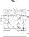
- FIG. 11 is a sectional view showing the multilayer structure of an element substrate according to the fourth embodiment. Note that the same reference numerals as already described with reference to FIGS. 5A, 5B, 6, 8, 9, and 10 denote similar constituent elements in FIG. 11 , and a description thereof will be omitted. A characteristic arrangement of the fourth embodiment will be described here.
- FIG. 12 is a plan view showing the schematic arrangement in the vicinity of a heater 101 on the element substrate.
- a temperature detection element 119 that is a thin-film resistor is formed using the same material.
- the temperature detection element 119 detects the temperature of the heater 101 , thereby detecting whether the heater normally operates, and ink is discharged.
- the outline of the temperature detection element is disclosed in Japanese Patent Laid-Open No. 2007-290361, and a detailed description thereof will be omitted here.
- Japanese Patent Laid-Open No. 2007-290361 discloses an element substrate in which a plurality of heaters configured to generate thermal energy to discharge ink are formed on a silicon substrate, and thin-film temperature detection elements are formed immediately under the heaters with an interlayer insulation film intervening between them.
- a temperature detection circuit detects temperature information from each temperature detection element, and determines, based on the difference between the temperature change of the heaters at the time of ink discharge failure and the temperature change of the heaters at the time of normal ink discharge, whether the ink discharge is normal, or a discharge failure has occurred. Temperature detection is performed by monitoring a change in the value of the electrical resistance of each temperature detection element.
- the temperature detection elements and the anticorrosion wiring layer are simultaneously built in when manufacturing the element substrate using a semiconductor manufacturing process, thereby reducing manufacturing processes.
- the printhead that discharges ink and the printing apparatus have been described as an example.
- the present invention is not limited to this.
- the present invention can be applied to an apparatus such as a printer, a copying machine, a facsimile including a communication system, or a word processor including a printer unit, and an industrial printing apparatus complexly combined with various kinds of processing apparatuses.
- the present invention can also be used for the purpose of, for example, biochip manufacture, electronic circuit printing, color filter manufacture, or the like.
- the printhead described in the above embodiments can also be considered as a liquid discharge head in general.
- the substance discharged from the head is not limited to ink, and can be considered as a liquid in general.
Landscapes
- Particle Formation And Scattering Control In Inkjet Printers (AREA)
- Physics & Mathematics (AREA)
- Thermal Sciences (AREA)
Abstract
Description
Claims (15)
Applications Claiming Priority (3)
| Application Number | Priority Date | Filing Date | Title |
|---|---|---|---|
| JP2019082197A JP7328787B2 (en) | 2019-04-23 | 2019-04-23 | ELEMENT SUBSTRATE, LIQUID EJECTION HEAD, AND RECORDING APPARATUS |
| JP2019-082197 | 2019-04-23 | ||
| JPJP2019-082197 | 2019-04-23 |
Publications (2)
| Publication Number | Publication Date |
|---|---|
| US20200338888A1 US20200338888A1 (en) | 2020-10-29 |
| US11383515B2 true US11383515B2 (en) | 2022-07-12 |
Family
ID=72916688
Family Applications (1)
| Application Number | Title | Priority Date | Filing Date |
|---|---|---|---|
| US16/848,983 Active US11383515B2 (en) | 2019-04-23 | 2020-04-15 | Element substrate, liquid discharge head, and printing apparatus |
Country Status (2)
| Country | Link |
|---|---|
| US (1) | US11383515B2 (en) |
| JP (1) | JP7328787B2 (en) |
Cited By (1)
| Publication number | Priority date | Publication date | Assignee | Title |
|---|---|---|---|---|
| US12246536B2 (en) | 2020-12-14 | 2025-03-11 | Canon Kabushiki Kaisha | Liquid ejection head substrate, liquid ejection head, and liquid ejection apparatus |
Families Citing this family (3)
| Publication number | Priority date | Publication date | Assignee | Title |
|---|---|---|---|---|
| TWI719864B (en) * | 2020-03-20 | 2021-02-21 | 研能科技股份有限公司 | Narrow type inkjet print head chip |
| JP2024131839A (en) * | 2023-03-16 | 2024-09-30 | キヤノン株式会社 | Substrate for liquid ejection head, liquid ejection head, and liquid ejection device |
| JP7739374B2 (en) * | 2023-09-27 | 2025-09-16 | キヤノン株式会社 | LIQUID EJECTION HEAD SUBSTRATE, LIQUID EJECTION HEAD, AND LIQUID EJECTION DEVICE |
Citations (9)
| Publication number | Priority date | Publication date | Assignee | Title |
|---|---|---|---|---|
| US5081474A (en) | 1988-07-04 | 1992-01-14 | Canon Kabushiki Kaisha | Recording head having multi-layer matrix wiring |
| US20070229566A1 (en) | 2006-03-31 | 2007-10-04 | Canon Kabushiki Kaisha | Liquid discharge head and liquid discharge apparatus using liquid discharge head |
| US20160152027A1 (en) | 2014-12-02 | 2016-06-02 | Canon Kabushiki Kaisha | Liquid discharge head and method for manufacturing the same |
| CN105818537A (en) | 2015-01-27 | 2016-08-03 | 佳能株式会社 | Element substrate and liquid ejection head |
| US20160297194A1 (en) | 2015-04-08 | 2016-10-13 | Canon Kabushiki Kaisha | Liquid ejection head |
| US10035346B2 (en) | 2015-01-27 | 2018-07-31 | Canon Kabushiki Kaisha | Element substrate and liquid ejection head |
| US20190001678A1 (en) | 2017-06-30 | 2019-01-03 | Canon Kabushiki Kaisha | Semiconductor device, method of manufacturing same, liquid discharge head, and liquid discharge apparatus |
| US20190001680A1 (en) * | 2017-06-30 | 2019-01-03 | Canon Kabushiki Kaisha | Element board, liquid ejection head, and printing apparatus |
| US20190105921A1 (en) * | 2017-10-11 | 2019-04-11 | Canon Kabushiki Kaisha | Element substrate, manufacturing method thereof, printhead, and printing apparatus |
Family Cites Families (2)
| Publication number | Priority date | Publication date | Assignee | Title |
|---|---|---|---|---|
| JP2008153275A (en) * | 2006-12-14 | 2008-07-03 | Canon Inc | Semiconductor substrate and manufacturing method thereof |
| CN105163943B (en) * | 2013-07-29 | 2017-06-23 | 惠普发展公司,有限责任合伙企业 | Fluid discharge apparatus |
-
2019
- 2019-04-23 JP JP2019082197A patent/JP7328787B2/en active Active
-
2020
- 2020-04-15 US US16/848,983 patent/US11383515B2/en active Active
Patent Citations (21)
| Publication number | Priority date | Publication date | Assignee | Title |
|---|---|---|---|---|
| US5081474A (en) | 1988-07-04 | 1992-01-14 | Canon Kabushiki Kaisha | Recording head having multi-layer matrix wiring |
| US20070229566A1 (en) | 2006-03-31 | 2007-10-04 | Canon Kabushiki Kaisha | Liquid discharge head and liquid discharge apparatus using liquid discharge head |
| JP2007290361A (en) | 2006-03-31 | 2007-11-08 | Canon Inc | Liquid discharge head and liquid discharge apparatus using the same |
| US7722148B2 (en) | 2006-03-31 | 2010-05-25 | Canon Kabushiki Kaisha | Liquid discharge head and liquid discharge apparatus using liquid discharge head |
| US20100194810A1 (en) | 2006-03-31 | 2010-08-05 | Canon Kabushiki Kaisha | Liquid discharge head and liquid discharge apparatus using liquid discharge head |
| US7950765B2 (en) | 2006-03-31 | 2011-05-31 | Canon Kabushiki Kaisha. | Liquid discharge head and liquid discharge apparatus using liquid discharge head |
| US20110164085A1 (en) | 2006-03-31 | 2011-07-07 | Canon Kabushiki Kaisha | Liquid discharge head and liquid discharge apparatus using liquid discharge head |
| US8172355B2 (en) | 2006-03-31 | 2012-05-08 | Canon Kabushiki Kaisha | Liquid discharge head and liquid discharge apparatus using liquid discharge head |
| US20160152027A1 (en) | 2014-12-02 | 2016-06-02 | Canon Kabushiki Kaisha | Liquid discharge head and method for manufacturing the same |
| JP2016137705A (en) | 2015-01-27 | 2016-08-04 | キヤノン株式会社 | Element substrate for liquid discharge head and liquid discharge head |
| CN105818537A (en) | 2015-01-27 | 2016-08-03 | 佳能株式会社 | Element substrate and liquid ejection head |
| US10035346B2 (en) | 2015-01-27 | 2018-07-31 | Canon Kabushiki Kaisha | Element substrate and liquid ejection head |
| US20180370233A1 (en) | 2015-01-27 | 2018-12-27 | Canon Kabushiki Kaisha | Element substrate and liquid ejection head |
| US20160297194A1 (en) | 2015-04-08 | 2016-10-13 | Canon Kabushiki Kaisha | Liquid ejection head |
| US20190001678A1 (en) | 2017-06-30 | 2019-01-03 | Canon Kabushiki Kaisha | Semiconductor device, method of manufacturing same, liquid discharge head, and liquid discharge apparatus |
| US20190001680A1 (en) * | 2017-06-30 | 2019-01-03 | Canon Kabushiki Kaisha | Element board, liquid ejection head, and printing apparatus |
| CN109203695A (en) | 2017-06-30 | 2019-01-15 | 佳能株式会社 | Semiconductor devices and its manufacturing method, liquid discharging head and liquid discharge device |
| US10543685B2 (en) | 2017-06-30 | 2020-01-28 | Canon Kabushiki Kaisha | Semiconductor device, method of manufacturing same, liquid discharge head, and liquid discharge apparatus |
| US20190105921A1 (en) * | 2017-10-11 | 2019-04-11 | Canon Kabushiki Kaisha | Element substrate, manufacturing method thereof, printhead, and printing apparatus |
| CN109649012A (en) | 2017-10-11 | 2019-04-19 | 佳能株式会社 | Device substrate, the manufacturing method of device substrate, print head and printing equipment |
| US10493774B2 (en) | 2017-10-11 | 2019-12-03 | Canon Kabushiki Kaisha | Element substrate, manufacturing method thereof, printhead, and printing apparatus |
Non-Patent Citations (1)
| Title |
|---|
| Co-Pending U.S. Appl. No. 16/848,975, filed Apr. 15, 2020. |
Cited By (1)
| Publication number | Priority date | Publication date | Assignee | Title |
|---|---|---|---|---|
| US12246536B2 (en) | 2020-12-14 | 2025-03-11 | Canon Kabushiki Kaisha | Liquid ejection head substrate, liquid ejection head, and liquid ejection apparatus |
Also Published As
| Publication number | Publication date |
|---|---|
| US20200338888A1 (en) | 2020-10-29 |
| JP2020179526A (en) | 2020-11-05 |
| JP7328787B2 (en) | 2023-08-17 |
Similar Documents
| Publication | Publication Date | Title |
|---|---|---|
| US11383515B2 (en) | Element substrate, liquid discharge head, and printing apparatus | |
| EP2135745B1 (en) | Liquid ejection head and method of manufacturing the liquid ejection head | |
| EP3470228B1 (en) | Element substrate, manufacturing method thereof, printhead, and printing apparatus | |
| US9096059B2 (en) | Substrate for inkjet head, inkjet head, and inkjet printing apparatus | |
| US20120062631A1 (en) | Recording head driving method and recording apparatus | |
| JP5677109B2 (en) | Inkjet recording head substrate, inkjet recording head, and recording apparatus | |
| JP7112287B2 (en) | ELEMENT SUBSTRATE, PRINT HEAD, PRINTING APPARATUS, AND METHOD FOR MANUFACTURING ELEMENT SUBSTRATE | |
| EP3730299B1 (en) | Element substrate, liquid discharge head, and printing apparatus | |
| JP6497902B2 (en) | Recording head substrate, recording head, and recording apparatus | |
| US9527281B2 (en) | Liquid ejection head and liquid ejection apparatus | |
| US11498333B2 (en) | Element substrate, liquid discharge head, and printing apparatus | |
| US11618254B2 (en) | Element substrate, liquid discharge head, and printing apparatus | |
| US11577508B2 (en) | Element substrate, liquid discharge head, and printing apparatus | |
| US20260054483A1 (en) | Element board | |
| CN113733750A (en) | Printing element substrate, printhead, and printing apparatus | |
| JP5317671B2 (en) | Substrate for liquid discharge head, liquid discharge head, and liquid discharge apparatus | |
| JP7465096B2 (en) | Element substrate, liquid ejection head, and recording apparatus | |
| US11155080B2 (en) | Cleaning method of liquid discharge head and liquid discharge apparatus | |
| JP5171377B2 (en) | Circuit board and liquid ejection device | |
| US9259926B2 (en) | Liquid ejection apparatus and liquid ejection head | |
| JP2001232796A (en) | Substrate for inkjet recording head, inkjet recording head, inkjet cartridge, and inkjet recording apparatus | |
| JP2023079429A (en) | Liquid ejector | |
| JP2019069533A (en) | Substrate for liquid discharge head, liquid discharge head, and cutting method for fuse part in the substrate | |
| JP2005085859A (en) | Circuit board manufacturing method |
Legal Events
| Date | Code | Title | Description |
|---|---|---|---|
| FEPP | Fee payment procedure |
Free format text: ENTITY STATUS SET TO UNDISCOUNTED (ORIGINAL EVENT CODE: BIG.); ENTITY STATUS OF PATENT OWNER: LARGE ENTITY |
|
| STPP | Information on status: patent application and granting procedure in general |
Free format text: DOCKETED NEW CASE - READY FOR EXAMINATION |
|
| AS | Assignment |
Owner name: CANON KABUSHIKI KAISHA, JAPAN Free format text: ASSIGNMENT OF ASSIGNORS INTEREST;ASSIGNORS:SAKUMA, SADAYOSHI;OSUKI, YOHEI;REEL/FRAME:053348/0765 Effective date: 20200401 |
|
| STPP | Information on status: patent application and granting procedure in general |
Free format text: NON FINAL ACTION MAILED |
|
| STPP | Information on status: patent application and granting procedure in general |
Free format text: RESPONSE TO NON-FINAL OFFICE ACTION ENTERED AND FORWARDED TO EXAMINER |
|
| STPP | Information on status: patent application and granting procedure in general |
Free format text: NOTICE OF ALLOWANCE MAILED -- APPLICATION RECEIVED IN OFFICE OF PUBLICATIONS |
|
| STPP | Information on status: patent application and granting procedure in general |
Free format text: AWAITING TC RESP., ISSUE FEE NOT PAID |
|
| STPP | Information on status: patent application and granting procedure in general |
Free format text: NOTICE OF ALLOWANCE MAILED -- APPLICATION RECEIVED IN OFFICE OF PUBLICATIONS |
|
| STCF | Information on status: patent grant |
Free format text: PATENTED CASE |
|
| MAFP | Maintenance fee payment |
Free format text: PAYMENT OF MAINTENANCE FEE, 4TH YEAR, LARGE ENTITY (ORIGINAL EVENT CODE: M1551); ENTITY STATUS OF PATENT OWNER: LARGE ENTITY Year of fee payment: 4 |