US11380853B2 - Organic light emitting diode and organic light emitting device including the same - Google Patents
Organic light emitting diode and organic light emitting device including the same Download PDFInfo
- Publication number
- US11380853B2 US11380853B2 US16/725,917 US201916725917A US11380853B2 US 11380853 B2 US11380853 B2 US 11380853B2 US 201916725917 A US201916725917 A US 201916725917A US 11380853 B2 US11380853 B2 US 11380853B2
- Authority
- US
- United States
- Prior art keywords
- host
- organic light
- light emitting
- formula
- electrode
- Prior art date
- Legal status (The legal status is an assumption and is not a legal conclusion. Google has not performed a legal analysis and makes no representation as to the accuracy of the status listed.)
- Active, expires
Links
- TXAPTJNNBOBPKG-UHFFFAOYSA-N CC1(C)c2ccccc2-c2ccc(N(c3ccc(-c4ccccc4)cc3)c3ccc4c(c3)C3(c5ccccc5-c5ccccc53)c3ccccc3-4)cc21.c1ccc(-c2ccc(N(c3ccc(-c4ccccc4)cc3)c3ccc4c(c3)C3(c5ccccc5-c5ccccc53)c3ccccc3-4)cc2)cc1.c1ccc(-c2ccc(N(c3ccc4c(c3)C3(c5ccccc5-c5ccccc53)c3ccccc3-4)c3ccccc3-c3ccccc3)cc2)cc1 Chemical compound CC1(C)c2ccccc2-c2ccc(N(c3ccc(-c4ccccc4)cc3)c3ccc4c(c3)C3(c5ccccc5-c5ccccc53)c3ccccc3-4)cc21.c1ccc(-c2ccc(N(c3ccc(-c4ccccc4)cc3)c3ccc4c(c3)C3(c5ccccc5-c5ccccc53)c3ccccc3-4)cc2)cc1.c1ccc(-c2ccc(N(c3ccc4c(c3)C3(c5ccccc5-c5ccccc53)c3ccccc3-4)c3ccccc3-c3ccccc3)cc2)cc1 TXAPTJNNBOBPKG-UHFFFAOYSA-N 0.000 description 3
- CTUOYKZQUPMPDC-UHFFFAOYSA-N CC1(C)c2ccccc2-c2ccc(N(c3ccc(-c4ccccc4)cc3)c3cccc4c3-c3ccccc3C43c4ccccc4-c4ccccc43)cc21.CC1(C)c2ccccc2-c2ccc(N(c3ccccc3-c3ccccc3)c3cccc4c3-c3ccccc3C43c4ccccc4-c4ccccc43)cc21.c1ccc(-c2ccc(N(c3ccc(-c4ccccc4)cc3)c3cccc4c3-c3ccccc3C43c4ccccc4-c4ccccc43)cc2)cc1.c1ccc(-c2ccc(N(c3ccccc3-c3ccccc3)c3cccc4c3-c3ccccc3C43c4ccccc4-c4ccccc43)cc2)cc1 Chemical compound CC1(C)c2ccccc2-c2ccc(N(c3ccc(-c4ccccc4)cc3)c3cccc4c3-c3ccccc3C43c4ccccc4-c4ccccc43)cc21.CC1(C)c2ccccc2-c2ccc(N(c3ccccc3-c3ccccc3)c3cccc4c3-c3ccccc3C43c4ccccc4-c4ccccc43)cc21.c1ccc(-c2ccc(N(c3ccc(-c4ccccc4)cc3)c3cccc4c3-c3ccccc3C43c4ccccc4-c4ccccc43)cc2)cc1.c1ccc(-c2ccc(N(c3ccccc3-c3ccccc3)c3cccc4c3-c3ccccc3C43c4ccccc4-c4ccccc43)cc2)cc1 CTUOYKZQUPMPDC-UHFFFAOYSA-N 0.000 description 3
- WXJFMYZMIXHHAV-UHFFFAOYSA-N CC1(C)c2ccccc2-c2ccc(N(c3ccc4c(c3)C(C)(C)c3ccccc3-4)c3ccc4c(c3)C3(c5ccccc5-c5ccccc53)c3ccccc3-4)cc21.CC1(C)c2ccccc2-c2ccc(N(c3ccc4c(c3)C3(c5ccccc5-c5ccccc53)c3ccccc3-4)c3ccccc3-c3ccccc3)cc21.c1ccc(-c2ccc(N(c3ccccc3)c3ccc4c(c3)C3(c5ccccc5-c5ccccc53)c3ccccc3-4)cc2)cc1.c1ccc(-c2ccc(N(c3ccccc3)c3cccc4c3-c3ccccc3C43c4ccccc4-c4ccccc43)cc2)cc1 Chemical compound CC1(C)c2ccccc2-c2ccc(N(c3ccc4c(c3)C(C)(C)c3ccccc3-4)c3ccc4c(c3)C3(c5ccccc5-c5ccccc53)c3ccccc3-4)cc21.CC1(C)c2ccccc2-c2ccc(N(c3ccc4c(c3)C3(c5ccccc5-c5ccccc53)c3ccccc3-4)c3ccccc3-c3ccccc3)cc21.c1ccc(-c2ccc(N(c3ccccc3)c3ccc4c(c3)C3(c5ccccc5-c5ccccc53)c3ccccc3-4)cc2)cc1.c1ccc(-c2ccc(N(c3ccccc3)c3cccc4c3-c3ccccc3C43c4ccccc4-c4ccccc43)cc2)cc1 WXJFMYZMIXHHAV-UHFFFAOYSA-N 0.000 description 3
- YERJFIFUANLSMW-UHFFFAOYSA-N CC1(C)c2ccccc2-c2ccc(N(c3ccc4c(c3)C(C)(C)c3ccccc3-4)c3cccc4c3-c3ccccc3C43c4ccccc4-c4ccccc43)cc21.c1ccc(-c2ccc(-c3ccc(N(c4ccccc4)c4ccc5c(c4)C4(c6ccccc6-c6ccccc64)c4ccccc4-5)cc3)cc2)cc1.c1ccc(N(c2ccc3c(c2)C2(c4ccccc4-c4ccccc42)c2ccccc2-3)c2ccc3c4ccccc4c4ccccc4c3c2)cc1.c1ccc(N(c2ccc3c(c2)C2(c4ccccc4-c4ccccc42)c2ccccc2-3)c2ccc3ccccc3c2)cc1 Chemical compound CC1(C)c2ccccc2-c2ccc(N(c3ccc4c(c3)C(C)(C)c3ccccc3-4)c3cccc4c3-c3ccccc3C43c4ccccc4-c4ccccc43)cc21.c1ccc(-c2ccc(-c3ccc(N(c4ccccc4)c4ccc5c(c4)C4(c6ccccc6-c6ccccc64)c4ccccc4-5)cc3)cc2)cc1.c1ccc(N(c2ccc3c(c2)C2(c4ccccc4-c4ccccc42)c2ccccc2-3)c2ccc3c4ccccc4c4ccccc4c3c2)cc1.c1ccc(N(c2ccc3c(c2)C2(c4ccccc4-c4ccccc42)c2ccccc2-3)c2ccc3ccccc3c2)cc1 YERJFIFUANLSMW-UHFFFAOYSA-N 0.000 description 3
- HPOAZTRNCWRQOV-UHFFFAOYSA-N c1ccc(-c2ccc(-c3cc(-n4c5ccccc5c5cc(-c6ccc7c(c6)c6ccccc6n7-c6ccccc6)ccc54)cc4c3oc3ccccc34)cc2)cc1.c1ccc(-c2ccc(-c3ccc(-n4c5ccccc5c5cc(-c6ccc7c(c6)c6ccccc6n7-c6ccccc6)ccc54)c4c3oc3ccccc34)cc2)cc1.c1ccc(-c2cccc(-c3cc(-n4c5ccccc5c5cc(-c6ccc7c(c6)c6ccccc6n7-c6ccccc6)ccc54)cc4c3oc3ccccc34)c2)cc1.c1ccc(-c2cccc(-c3ccc(-c4cc(-n5c6ccccc6c6cc(-c7ccc8c(c7)c7ccccc7n8-c7ccccc7)ccc65)cc5c4oc4ccccc45)cc3)c2)cc1 Chemical compound c1ccc(-c2ccc(-c3cc(-n4c5ccccc5c5cc(-c6ccc7c(c6)c6ccccc6n7-c6ccccc6)ccc54)cc4c3oc3ccccc34)cc2)cc1.c1ccc(-c2ccc(-c3ccc(-n4c5ccccc5c5cc(-c6ccc7c(c6)c6ccccc6n7-c6ccccc6)ccc54)c4c3oc3ccccc34)cc2)cc1.c1ccc(-c2cccc(-c3cc(-n4c5ccccc5c5cc(-c6ccc7c(c6)c6ccccc6n7-c6ccccc6)ccc54)cc4c3oc3ccccc34)c2)cc1.c1ccc(-c2cccc(-c3ccc(-c4cc(-n5c6ccccc6c6cc(-c7ccc8c(c7)c7ccccc7n8-c7ccccc7)ccc65)cc5c4oc4ccccc45)cc3)c2)cc1 HPOAZTRNCWRQOV-UHFFFAOYSA-N 0.000 description 3
- QJIRYNKBDPIZNL-UHFFFAOYSA-N c1ccc(-c2nc(-c3ccccc3)nc(-c3ccc4oc5ccc(-c6ccc7c(c6)c6ccccc6n7-c6ccccc6)cc5c4c3)n2)cc1.c1ccc(-c2nc(-c3ccccc3)nc(-c3ccc4oc5ccc(-n6c7ccccc7c7ccccc76)cc5c4c3)n2)cc1.c1ccc(-c2nc(-c3ccccc3)nc(-c3cccc(-n4c5ccccc5c5cc(-c6ccc7c(c6)c6ccccc6n7-c6ccccc6)ccc54)c3)n2)cc1.c1ccc(-c2nc(-c3ccccc3)nc(-n3c4ccccc4c4cc5c6ccccc6n(-c6ccccc6)c5cc43)n2)cc1 Chemical compound c1ccc(-c2nc(-c3ccccc3)nc(-c3ccc4oc5ccc(-c6ccc7c(c6)c6ccccc6n7-c6ccccc6)cc5c4c3)n2)cc1.c1ccc(-c2nc(-c3ccccc3)nc(-c3ccc4oc5ccc(-n6c7ccccc7c7ccccc76)cc5c4c3)n2)cc1.c1ccc(-c2nc(-c3ccccc3)nc(-c3cccc(-n4c5ccccc5c5cc(-c6ccc7c(c6)c6ccccc6n7-c6ccccc6)ccc54)c3)n2)cc1.c1ccc(-c2nc(-c3ccccc3)nc(-n3c4ccccc4c4cc5c6ccccc6n(-c6ccccc6)c5cc43)n2)cc1 QJIRYNKBDPIZNL-UHFFFAOYSA-N 0.000 description 3
- WVBRUSAVITZPBH-UHFFFAOYSA-N c1ccc(N(c2ccc3c(c2)C2(c4ccccc4-c4ccccc42)c2ccccc2-3)c2cc3ccccc3c3ccccc23)cc1.c1ccc(N(c2ccc3c(c2)C2(c4ccccc4-c4ccccc42)c2ccccc2-3)c2ccc3c(c2)oc2ccccc23)cc1.c1ccc(N(c2ccc3c(c2)C2(c4ccccc4-c4ccccc42)c2ccccc2-3)c2ccc3c(c2)sc2ccccc23)cc1 Chemical compound c1ccc(N(c2ccc3c(c2)C2(c4ccccc4-c4ccccc42)c2ccccc2-3)c2cc3ccccc3c3ccccc23)cc1.c1ccc(N(c2ccc3c(c2)C2(c4ccccc4-c4ccccc42)c2ccccc2-3)c2ccc3c(c2)oc2ccccc23)cc1.c1ccc(N(c2ccc3c(c2)C2(c4ccccc4-c4ccccc42)c2ccccc2-3)c2ccc3c(c2)sc2ccccc23)cc1 WVBRUSAVITZPBH-UHFFFAOYSA-N 0.000 description 3
- 0 CC.CC.Cn1c2ccccc2c2ccccc21.[15*]C.c1ccc2c(c1)Cc1ccccc1-2 Chemical compound CC.CC.Cn1c2ccccc2c2ccccc21.[15*]C.c1ccc2c(c1)Cc1ccccc1-2 0.000 description 2
- OBZJPVAGBHHPPV-UHFFFAOYSA-N c1ccc(-c2ccc(-c3c(-n4c5ccccc5c5cc(-c6ccc7c(c6)c6ccccc6n7-c6ccccc6)ccc54)ccc4c3sc3ccccc34)cc2)cc1.c1ccc(-c2ccc(-c3cc(-n4c5ccccc5c5cc(-c6ccc7c(c6)c6ccccc6n7-c6ccccc6)ccc54)cc4c3sc3ccccc34)cc2)cc1.c1ccc(-c2ccc(-c3ccc(-n4c5ccccc5c5cc(-c6ccc7c(c6)c6ccccc6n7-c6ccccc6)ccc54)c4c3sc3ccccc34)cc2)cc1.c1ccc(-c2cccc(-c3cc(-n4c5ccccc5c5cc(-c6ccc7c(c6)c6ccccc6n7-c6ccccc6)ccc54)cc4c3sc3ccccc34)c2)cc1 Chemical compound c1ccc(-c2ccc(-c3c(-n4c5ccccc5c5cc(-c6ccc7c(c6)c6ccccc6n7-c6ccccc6)ccc54)ccc4c3sc3ccccc34)cc2)cc1.c1ccc(-c2ccc(-c3cc(-n4c5ccccc5c5cc(-c6ccc7c(c6)c6ccccc6n7-c6ccccc6)ccc54)cc4c3sc3ccccc34)cc2)cc1.c1ccc(-c2ccc(-c3ccc(-n4c5ccccc5c5cc(-c6ccc7c(c6)c6ccccc6n7-c6ccccc6)ccc54)c4c3sc3ccccc34)cc2)cc1.c1ccc(-c2cccc(-c3cc(-n4c5ccccc5c5cc(-c6ccc7c(c6)c6ccccc6n7-c6ccccc6)ccc54)cc4c3sc3ccccc34)c2)cc1 OBZJPVAGBHHPPV-UHFFFAOYSA-N 0.000 description 2
- IOVGQJLOIWNLOP-UHFFFAOYSA-N c1ccc(-c2ccc(-c3cc(-n4c5ccc(-c6ccccc6)cc5c5cc(-c6ccc7c(c6)c6cc(-c8ccccc8)ccc6n7-c6ccccc6)ccc54)cc4c3oc3ccc(-c5ccccc5)cc34)cc2)cc1.c1ccc(-c2ccc(-c3cc(-n4c5ccccc5c5cc(-c6ccc7c(c6)c6cc(-c8ccccc8)ccc6n7-c6ccccc6)ccc54)cc4c3oc3ccc(-c5ccccc5)cc34)cc2)cc1 Chemical compound c1ccc(-c2ccc(-c3cc(-n4c5ccc(-c6ccccc6)cc5c5cc(-c6ccc7c(c6)c6cc(-c8ccccc8)ccc6n7-c6ccccc6)ccc54)cc4c3oc3ccc(-c5ccccc5)cc34)cc2)cc1.c1ccc(-c2ccc(-c3cc(-n4c5ccccc5c5cc(-c6ccc7c(c6)c6cc(-c8ccccc8)ccc6n7-c6ccccc6)ccc54)cc4c3oc3ccc(-c5ccccc5)cc34)cc2)cc1 IOVGQJLOIWNLOP-UHFFFAOYSA-N 0.000 description 2
- BJTMJEUCRURLIA-UHFFFAOYSA-N c1ccc(-c2ccc(-c3cc(-n4c5ccc(-c6ccccc6)cc5c5cc(-c6ccc7c(c6)c6cc(-c8ccccc8)ccc6n7-c6ccccc6)ccc54)cc4c3sc3ccc(-c5ccccc5)cc34)cc2)cc1.c1ccc(-c2ccc(-c3cc(-n4c5ccc(-c6ccccc6)cc5c5cc(-c6ccc7c(c6)c6ccccc6n7-c6ccccc6)ccc54)cc4c3sc3ccccc34)cc2)cc1.c1ccc(-c2ccc(-c3cc(-n4c5ccccc5c5cc(-c6ccc7c(c6)c6cc(-c8ccccc8)ccc6n7-c6ccccc6)ccc54)cc4c3sc3ccc(-c5ccccc5)cc34)cc2)cc1 Chemical compound c1ccc(-c2ccc(-c3cc(-n4c5ccc(-c6ccccc6)cc5c5cc(-c6ccc7c(c6)c6cc(-c8ccccc8)ccc6n7-c6ccccc6)ccc54)cc4c3sc3ccc(-c5ccccc5)cc34)cc2)cc1.c1ccc(-c2ccc(-c3cc(-n4c5ccc(-c6ccccc6)cc5c5cc(-c6ccc7c(c6)c6ccccc6n7-c6ccccc6)ccc54)cc4c3sc3ccccc34)cc2)cc1.c1ccc(-c2ccc(-c3cc(-n4c5ccccc5c5cc(-c6ccc7c(c6)c6cc(-c8ccccc8)ccc6n7-c6ccccc6)ccc54)cc4c3sc3ccc(-c5ccccc5)cc34)cc2)cc1 BJTMJEUCRURLIA-UHFFFAOYSA-N 0.000 description 2
- RBXBFBWJAWCXDM-UHFFFAOYSA-N c1ccc(-c2ccc(-c3cc(-n4c5ccc(-c6ccccc6)cc5c5cc(-c6ccc7c(c6)c6ccccc6n7-c6ccccc6)ccc54)cc4c3oc3ccccc34)cc2)cc1.c1ccc(-c2ccc(-c3cc(-n4c5ccccc5c5cc(-c6ccc7c(c6)c6cc(-c8ccccc8)ccc6n7-c6ccccc6)ccc54)cc4c3oc3ccccc34)cc2)cc1.c1ccc(-c2ccc(-c3cc(-n4c5ccccc5c5cc(-c6ccc7c(c6)c6ccccc6n7-c6ccccc6)ccc54)cc4c3oc3ccc(-c5ccccc5)cc34)cc2)cc1 Chemical compound c1ccc(-c2ccc(-c3cc(-n4c5ccc(-c6ccccc6)cc5c5cc(-c6ccc7c(c6)c6ccccc6n7-c6ccccc6)ccc54)cc4c3oc3ccccc34)cc2)cc1.c1ccc(-c2ccc(-c3cc(-n4c5ccccc5c5cc(-c6ccc7c(c6)c6cc(-c8ccccc8)ccc6n7-c6ccccc6)ccc54)cc4c3oc3ccccc34)cc2)cc1.c1ccc(-c2ccc(-c3cc(-n4c5ccccc5c5cc(-c6ccc7c(c6)c6ccccc6n7-c6ccccc6)ccc54)cc4c3oc3ccc(-c5ccccc5)cc34)cc2)cc1 RBXBFBWJAWCXDM-UHFFFAOYSA-N 0.000 description 2
- BAVCDNDYNFBMTP-UHFFFAOYSA-N c1ccc(-c2ccc(-c3cc(-n4c5ccccc5c5cc(-c6ccc7c(c6)c6cc(-c8ccccc8)ccc6n7-c6ccccc6)ccc54)cc4c3sc3ccccc34)cc2)cc1.c1ccc(-c2ccc(-c3cc(-n4c5ccccc5c5cc(-c6ccc7c(c6)c6ccccc6n7-c6ccccc6)ccc54)cc4c3sc3ccc(-c5ccccc5)cc34)cc2)cc1.c1ccc(-n2c3ccccc3c3cc(-c4ccc5c(c4)c4ccccc4n5-c4cc(-c5ccc6c(c5)-c5ccccc5C6)c5sc6ccccc6c5c4)ccc32)cc1 Chemical compound c1ccc(-c2ccc(-c3cc(-n4c5ccccc5c5cc(-c6ccc7c(c6)c6cc(-c8ccccc8)ccc6n7-c6ccccc6)ccc54)cc4c3sc3ccccc34)cc2)cc1.c1ccc(-c2ccc(-c3cc(-n4c5ccccc5c5cc(-c6ccc7c(c6)c6ccccc6n7-c6ccccc6)ccc54)cc4c3sc3ccc(-c5ccccc5)cc34)cc2)cc1.c1ccc(-n2c3ccccc3c3cc(-c4ccc5c(c4)c4ccccc4n5-c4cc(-c5ccc6c(c5)-c5ccccc5C6)c5sc6ccccc6c5c4)ccc32)cc1 BAVCDNDYNFBMTP-UHFFFAOYSA-N 0.000 description 2
- QWRYLPLNCVABJM-UHFFFAOYSA-N c1ccc(-c2ccc(-c3cc(-n4c5ccccc5c5cc(-c6ccc7c(c6)c6ccccc6n7-c6ccc(-c7ccccc7)cc6)ccc54)cc4c3sc3ccccc34)cc2)cc1.c1ccc(-c2ccc(-c3cc(-n4c5ccccc5c5cc(-c6ccc7c(c6)c6ccccc6n7-c6cccc(-c7ccccc7)c6)ccc54)cc4c3sc3ccccc34)cc2)cc1.c1ccc(-c2cccc(-c3cc(-n4c5ccccc5c5cc(-c6ccc7c(c6)c6ccccc6n7-c6cccc(-c7ccccc7)c6)ccc54)cc4c3sc3ccccc34)c2)cc1.c1ccc(-n2c3ccccc3c3cc(-c4ccc5c(c4)c4ccccc4n5-c4cc(-c5cccc6ccccc56)c5sc6ccccc6c5c4)ccc32)cc1 Chemical compound c1ccc(-c2ccc(-c3cc(-n4c5ccccc5c5cc(-c6ccc7c(c6)c6ccccc6n7-c6ccc(-c7ccccc7)cc6)ccc54)cc4c3sc3ccccc34)cc2)cc1.c1ccc(-c2ccc(-c3cc(-n4c5ccccc5c5cc(-c6ccc7c(c6)c6ccccc6n7-c6cccc(-c7ccccc7)c6)ccc54)cc4c3sc3ccccc34)cc2)cc1.c1ccc(-c2cccc(-c3cc(-n4c5ccccc5c5cc(-c6ccc7c(c6)c6ccccc6n7-c6cccc(-c7ccccc7)c6)ccc54)cc4c3sc3ccccc34)c2)cc1.c1ccc(-n2c3ccccc3c3cc(-c4ccc5c(c4)c4ccccc4n5-c4cc(-c5cccc6ccccc56)c5sc6ccccc6c5c4)ccc32)cc1 QWRYLPLNCVABJM-UHFFFAOYSA-N 0.000 description 2
- CBAKQUBQCQQOJQ-UHFFFAOYSA-N c1ccc(-c2cccc(-c3ccc(-c4cc(-n5c6ccccc6c6cc(-c7ccc8c(c7)c7ccccc7n8-c7ccccc7)ccc65)cc5c4sc4ccccc45)cc3)c2)cc1.c1ccc(-n2c3ccccc3c3cc(-c4ccc5c(c4)c4ccccc4n5-c4cc(-c5ccc6c(c5)-c5cccc7cccc-6c57)c5sc6ccccc6c5c4)ccc32)cc1.c1ccc(-n2c3ccccc3c3cc(-c4ccc5c(c4)c4ccccc4n5-c4cc(-c5ccc6c7ccccc7c7ccccc7c6c5)c5sc6ccccc6c5c4)ccc32)cc1.c1ccc(-n2c3ccccc3c3cc(-c4ccc5c(c4)c4ccccc4n5-c4cc(-c5ccc6ccc7ccccc7c6c5)c5sc6ccccc6c5c4)ccc32)cc1 Chemical compound c1ccc(-c2cccc(-c3ccc(-c4cc(-n5c6ccccc6c6cc(-c7ccc8c(c7)c7ccccc7n8-c7ccccc7)ccc65)cc5c4sc4ccccc45)cc3)c2)cc1.c1ccc(-n2c3ccccc3c3cc(-c4ccc5c(c4)c4ccccc4n5-c4cc(-c5ccc6c(c5)-c5cccc7cccc-6c57)c5sc6ccccc6c5c4)ccc32)cc1.c1ccc(-n2c3ccccc3c3cc(-c4ccc5c(c4)c4ccccc4n5-c4cc(-c5ccc6c7ccccc7c7ccccc7c6c5)c5sc6ccccc6c5c4)ccc32)cc1.c1ccc(-n2c3ccccc3c3cc(-c4ccc5c(c4)c4ccccc4n5-c4cc(-c5ccc6ccc7ccccc7c6c5)c5sc6ccccc6c5c4)ccc32)cc1 CBAKQUBQCQQOJQ-UHFFFAOYSA-N 0.000 description 2
- GIGYBPQQKLFJOC-UHFFFAOYSA-N c1ccc(-n2c3ccccc3c3cc(-c4ccc5c(c4)c4ccccc4n5-c4cc(-c5ccc6c(c5)-c5cccc7cccc-6c57)c5oc6ccccc6c5c4)ccc32)cc1.c1ccc(-n2c3ccccc3c3cc(-c4ccc5c(c4)c4ccccc4n5-c4cc(-c5ccc6c(c5)-c5ccccc5C6)c5oc6ccccc6c5c4)ccc32)cc1.c1ccc(-n2c3ccccc3c3cc(-c4ccc5c(c4)c4ccccc4n5-c4cc(-c5ccc6c7ccccc7c7ccccc7c6c5)c5oc6ccccc6c5c4)ccc32)cc1.c1ccc(-n2c3ccccc3c3cc(-c4ccc5c(c4)c4ccccc4n5-c4cc(-c5ccc6ccc7ccccc7c6c5)c5oc6ccccc6c5c4)ccc32)cc1 Chemical compound c1ccc(-n2c3ccccc3c3cc(-c4ccc5c(c4)c4ccccc4n5-c4cc(-c5ccc6c(c5)-c5cccc7cccc-6c57)c5oc6ccccc6c5c4)ccc32)cc1.c1ccc(-n2c3ccccc3c3cc(-c4ccc5c(c4)c4ccccc4n5-c4cc(-c5ccc6c(c5)-c5ccccc5C6)c5oc6ccccc6c5c4)ccc32)cc1.c1ccc(-n2c3ccccc3c3cc(-c4ccc5c(c4)c4ccccc4n5-c4cc(-c5ccc6c7ccccc7c7ccccc7c6c5)c5oc6ccccc6c5c4)ccc32)cc1.c1ccc(-n2c3ccccc3c3cc(-c4ccc5c(c4)c4ccccc4n5-c4cc(-c5ccc6ccc7ccccc7c6c5)c5oc6ccccc6c5c4)ccc32)cc1 GIGYBPQQKLFJOC-UHFFFAOYSA-N 0.000 description 2
- KDOQTPLAMKIRAX-UHFFFAOYSA-N c1ccc(-n2c3ccccc3c3cc(-c4ccc5c(c4)c4ccccc4n5-c4cc(-c5ccc6ccccc6c5)c5sc6ccccc6c5c4)ccc32)cc1 Chemical compound c1ccc(-n2c3ccccc3c3cc(-c4ccc5c(c4)c4ccccc4n5-c4cc(-c5ccc6ccccc6c5)c5sc6ccccc6c5c4)ccc32)cc1 KDOQTPLAMKIRAX-UHFFFAOYSA-N 0.000 description 2
- VWQYNNBIABFLKM-UHFFFAOYSA-N Brc1ccc(-c2ccccc2)cc1.OB(O)c1cc(-n2c3ccccc3c3cc(-c4ccc5c(c4)c4ccccc4n5-c4ccccc4)ccc32)cc2c1sc1ccccc12.[H-].c1ccc(-c2ccc(-c3cc(-n4c5ccccc5c5cc(-c6ccc7c(c6)c6ccccc6n7-c6ccccc6)ccc54)cc4c3sc3ccccc34)cc2)cc1 Chemical compound Brc1ccc(-c2ccccc2)cc1.OB(O)c1cc(-n2c3ccccc3c3cc(-c4ccc5c(c4)c4ccccc4n5-c4ccccc4)ccc32)cc2c1sc1ccccc12.[H-].c1ccc(-c2ccc(-c3cc(-n4c5ccccc5c5cc(-c6ccc7c(c6)c6ccccc6n7-c6ccccc6)ccc54)cc4c3sc3ccccc34)cc2)cc1 VWQYNNBIABFLKM-UHFFFAOYSA-N 0.000 description 1
- BCEYYOMWNYHYNR-UHFFFAOYSA-N CC.CC.CC.CC.CC.CC.CC.CC.[Y][Y][Y][Y]1=[Y]([Y][Y])[Y]([Y])=[Y]c2oc3c4-c5ccccn5->[Ir@@]5(c6ccccc6-c6ccccn->56)c4ccc3c21.c1ccc2[Ir]3(c4ccccc4-c4ccccn->34)<-n3ccccc3-c2c1 Chemical compound CC.CC.CC.CC.CC.CC.CC.CC.[Y][Y][Y][Y]1=[Y]([Y][Y])[Y]([Y])=[Y]c2oc3c4-c5ccccn5->[Ir@@]5(c6ccccc6-c6ccccn->56)c4ccc3c21.c1ccc2[Ir]3(c4ccccc4-c4ccccn->34)<-n3ccccc3-c2c1 BCEYYOMWNYHYNR-UHFFFAOYSA-N 0.000 description 1
- ZUUQXKDOSBCJRC-UHFFFAOYSA-N CC1(C)c2ccccc2-c2ccc([SH](c3ccc(-c4ccccc4)cc3)c3ccc(-c4ccc5c(c4)c4ccccc4n5-c4ccccc4)cc3)cc21.c1ccc(-n2c(-c3ccc(-c4ccc5c(-c6ccc7ccccc7c6)c6ccccc6c(-c6ccc7ccccc7c6)c5c4)cc3)nc3ccccc32)cc1.c1ccc(-n2c3ccccc3c3cc(-c4ccc5c(c4)c4ccccc4n5-c4ccccc4)ccc32)cc1 Chemical compound CC1(C)c2ccccc2-c2ccc([SH](c3ccc(-c4ccccc4)cc3)c3ccc(-c4ccc5c(c4)c4ccccc4n5-c4ccccc4)cc3)cc21.c1ccc(-n2c(-c3ccc(-c4ccc5c(-c6ccc7ccccc7c6)c6ccccc6c(-c6ccc7ccccc7c6)c5c4)cc3)nc3ccccc32)cc1.c1ccc(-n2c3ccccc3c3cc(-c4ccc5c(c4)c4ccccc4n5-c4ccccc4)ccc32)cc1 ZUUQXKDOSBCJRC-UHFFFAOYSA-N 0.000 description 1
- GTQIAEVMWZGIEL-UHFFFAOYSA-N c1ccc(-c2ccc(-c3c(-n4c5ccccc5c5cc(-c6ccc7c(c6)c6ccccc6n7-c6ccccc6)ccc54)ccc4c3sc3ccccc34)cc2)cc1.c1ccc(-c2ccc(-c3cc(-n4c5ccccc5c5cc(-c6ccc7c(c6)c6ccccc6n7-c6ccccc6)ccc54)cc4c3sc3ccccc34)cc2)cc1.c1ccc(-c2ccc(-c3ccc(-n4c5ccccc5c5cc(-c6ccc7c(c6)c6ccccc6n7-c6ccccc6)ccc54)c4c3sc3ccccc34)cc2)cc1 Chemical compound c1ccc(-c2ccc(-c3c(-n4c5ccccc5c5cc(-c6ccc7c(c6)c6ccccc6n7-c6ccccc6)ccc54)ccc4c3sc3ccccc34)cc2)cc1.c1ccc(-c2ccc(-c3cc(-n4c5ccccc5c5cc(-c6ccc7c(c6)c6ccccc6n7-c6ccccc6)ccc54)cc4c3sc3ccccc34)cc2)cc1.c1ccc(-c2ccc(-c3ccc(-n4c5ccccc5c5cc(-c6ccc7c(c6)c6ccccc6n7-c6ccccc6)ccc54)c4c3sc3ccccc34)cc2)cc1 GTQIAEVMWZGIEL-UHFFFAOYSA-N 0.000 description 1
- BVKVANDSVNDRBS-UHFFFAOYSA-N c1ccc(-c2ccc(-c3cc(-n4c5ccc(-c6ccccc6)cc5c5cc(-c6ccc7c(c6)c6cc(-c8ccccc8)ccc6n7-c6ccccc6)ccc54)cc4c3oc3ccc(-c5ccccc5)cc34)cc2)cc1.c1ccc(-c2ccc(-c3cc(-n4c5ccc(-c6ccccc6)cc5c5cc(-c6ccc7c(c6)c6ccccc6n7-c6ccccc6)ccc54)cc4c3oc3ccccc34)cc2)cc1.c1ccc(-c2ccc(-c3cc(-n4c5ccccc5c5cc(-c6ccc7c(c6)c6cc(-c8ccccc8)ccc6n7-c6ccccc6)ccc54)cc4c3oc3ccc(-c5ccccc5)cc34)cc2)cc1 Chemical compound c1ccc(-c2ccc(-c3cc(-n4c5ccc(-c6ccccc6)cc5c5cc(-c6ccc7c(c6)c6cc(-c8ccccc8)ccc6n7-c6ccccc6)ccc54)cc4c3oc3ccc(-c5ccccc5)cc34)cc2)cc1.c1ccc(-c2ccc(-c3cc(-n4c5ccc(-c6ccccc6)cc5c5cc(-c6ccc7c(c6)c6ccccc6n7-c6ccccc6)ccc54)cc4c3oc3ccccc34)cc2)cc1.c1ccc(-c2ccc(-c3cc(-n4c5ccccc5c5cc(-c6ccc7c(c6)c6cc(-c8ccccc8)ccc6n7-c6ccccc6)ccc54)cc4c3oc3ccc(-c5ccccc5)cc34)cc2)cc1 BVKVANDSVNDRBS-UHFFFAOYSA-N 0.000 description 1
- HWWXYYZNXQWUPD-UHFFFAOYSA-N c1ccc(-c2ccc(-c3cc(-n4c5ccc(-c6ccccc6)cc5c5cc(-c6ccc7c(c6)c6cc(-c8ccccc8)ccc6n7-c6ccccc6)ccc54)cc4c3sc3ccc(-c5ccccc5)cc34)cc2)cc1.c1ccc(-c2ccc(-c3cc(-n4c5ccccc5c5cc(-c6ccc7c(c6)c6cc(-c8ccccc8)ccc6n7-c6ccccc6)ccc54)cc4c3sc3ccc(-c5ccccc5)cc34)cc2)cc1 Chemical compound c1ccc(-c2ccc(-c3cc(-n4c5ccc(-c6ccccc6)cc5c5cc(-c6ccc7c(c6)c6cc(-c8ccccc8)ccc6n7-c6ccccc6)ccc54)cc4c3sc3ccc(-c5ccccc5)cc34)cc2)cc1.c1ccc(-c2ccc(-c3cc(-n4c5ccccc5c5cc(-c6ccc7c(c6)c6cc(-c8ccccc8)ccc6n7-c6ccccc6)ccc54)cc4c3sc3ccc(-c5ccccc5)cc34)cc2)cc1 HWWXYYZNXQWUPD-UHFFFAOYSA-N 0.000 description 1
- KWQDKKLAXNGBHP-UHFFFAOYSA-N c1ccc(-c2ccc(-c3cc(-n4c5ccc(-c6ccccc6)cc5c5cc(-c6ccc7c(c6)c6ccccc6n7-c6ccccc6)ccc54)cc4c3sc3ccccc34)cc2)cc1.c1ccc(-c2ccc(-c3cc(-n4c5ccccc5c5cc(-c6ccc7c(c6)c6cc(-c8ccccc8)ccc6n7-c6ccccc6)ccc54)cc4c3sc3ccccc34)cc2)cc1.c1ccc(-c2ccc(-c3cc(-n4c5ccccc5c5cc(-c6ccc7c(c6)c6ccccc6n7-c6ccccc6)ccc54)cc4c3sc3ccc(-c5ccccc5)cc34)cc2)cc1 Chemical compound c1ccc(-c2ccc(-c3cc(-n4c5ccc(-c6ccccc6)cc5c5cc(-c6ccc7c(c6)c6ccccc6n7-c6ccccc6)ccc54)cc4c3sc3ccccc34)cc2)cc1.c1ccc(-c2ccc(-c3cc(-n4c5ccccc5c5cc(-c6ccc7c(c6)c6cc(-c8ccccc8)ccc6n7-c6ccccc6)ccc54)cc4c3sc3ccccc34)cc2)cc1.c1ccc(-c2ccc(-c3cc(-n4c5ccccc5c5cc(-c6ccc7c(c6)c6ccccc6n7-c6ccccc6)ccc54)cc4c3sc3ccc(-c5ccccc5)cc34)cc2)cc1 KWQDKKLAXNGBHP-UHFFFAOYSA-N 0.000 description 1
- WOIUGDGVPYDDTE-UHFFFAOYSA-N c1ccc(-c2ccc(-c3cc(-n4c5ccccc5c5cc(-c6ccc7c(c6)c6cc(-c8ccccc8)ccc6n7-c6ccccc6)ccc54)cc4c3oc3ccccc34)cc2)cc1.c1ccc(-c2ccc(-c3cc(-n4c5ccccc5c5cc(-c6ccc7c(c6)c6ccccc6n7-c6ccccc6)ccc54)cc4c3oc3ccc(-c5ccccc5)cc34)cc2)cc1.c1ccc(-n2c3ccccc3c3cc(-c4ccc5c(c4)c4ccccc4n5-c4cc(-c5ccc6c(c5)-c5ccccc5C6)c5oc6ccccc6c5c4)ccc32)cc1 Chemical compound c1ccc(-c2ccc(-c3cc(-n4c5ccccc5c5cc(-c6ccc7c(c6)c6cc(-c8ccccc8)ccc6n7-c6ccccc6)ccc54)cc4c3oc3ccccc34)cc2)cc1.c1ccc(-c2ccc(-c3cc(-n4c5ccccc5c5cc(-c6ccc7c(c6)c6ccccc6n7-c6ccccc6)ccc54)cc4c3oc3ccc(-c5ccccc5)cc34)cc2)cc1.c1ccc(-n2c3ccccc3c3cc(-c4ccc5c(c4)c4ccccc4n5-c4cc(-c5ccc6c(c5)-c5ccccc5C6)c5oc6ccccc6c5c4)ccc32)cc1 WOIUGDGVPYDDTE-UHFFFAOYSA-N 0.000 description 1
- RBKIKMGFXTYFOI-UHFFFAOYSA-N c1ccc(-c2ccc(-c3cc(-n4c5ccccc5c5cc(-c6ccc7c(c6)c6ccccc6n7-c6ccc(-c7ccccc7)cc6)ccc54)cc4c3sc3ccccc34)cc2)cc1.c1ccc(-c2ccc(-c3cc(-n4c5ccccc5c5cc(-c6ccc7c(c6)c6ccccc6n7-c6cccc(-c7ccccc7)c6)ccc54)cc4c3sc3ccccc34)cc2)cc1.c1ccc(-c2cccc(-c3cc(-n4c5ccccc5c5cc(-c6ccc7c(c6)c6ccccc6n7-c6cccc(-c7ccccc7)c6)ccc54)cc4c3sc3ccccc34)c2)cc1.c1ccc(-c2cccc(-c3ccc(-c4cc(-n5c6ccccc6c6cc(-c7ccc8c(c7)c7ccccc7n8-c7ccccc7)ccc65)cc5c4sc4ccccc45)cc3)c2)cc1 Chemical compound c1ccc(-c2ccc(-c3cc(-n4c5ccccc5c5cc(-c6ccc7c(c6)c6ccccc6n7-c6ccc(-c7ccccc7)cc6)ccc54)cc4c3sc3ccccc34)cc2)cc1.c1ccc(-c2ccc(-c3cc(-n4c5ccccc5c5cc(-c6ccc7c(c6)c6ccccc6n7-c6cccc(-c7ccccc7)c6)ccc54)cc4c3sc3ccccc34)cc2)cc1.c1ccc(-c2cccc(-c3cc(-n4c5ccccc5c5cc(-c6ccc7c(c6)c6ccccc6n7-c6cccc(-c7ccccc7)c6)ccc54)cc4c3sc3ccccc34)c2)cc1.c1ccc(-c2cccc(-c3ccc(-c4cc(-n5c6ccccc6c6cc(-c7ccc8c(c7)c7ccccc7n8-c7ccccc7)ccc65)cc5c4sc4ccccc45)cc3)c2)cc1 RBKIKMGFXTYFOI-UHFFFAOYSA-N 0.000 description 1
- OUUMDGQJIOAHEY-UHFFFAOYSA-N c1ccc(-c2cccc(-c3cc(-n4c5ccccc5c5cc(-c6ccc7c(c6)c6ccccc6n7-c6ccccc6)ccc54)cc4c3sc3ccccc34)c2)cc1.c1ccc(-n2c3ccccc3c3cc(-c4ccc5c(c4)c4ccccc4n5-c4cc(-c5ccc6ccccc6c5)c5sc6ccccc6c5c4)ccc32)cc1.c1ccc(-n2c3ccccc3c3cc(-c4ccc5c(c4)c4ccccc4n5-c4cc(-c5cccc6ccccc56)c5sc6ccccc6c5c4)ccc32)cc1 Chemical compound c1ccc(-c2cccc(-c3cc(-n4c5ccccc5c5cc(-c6ccc7c(c6)c6ccccc6n7-c6ccccc6)ccc54)cc4c3sc3ccccc34)c2)cc1.c1ccc(-n2c3ccccc3c3cc(-c4ccc5c(c4)c4ccccc4n5-c4cc(-c5ccc6ccccc6c5)c5sc6ccccc6c5c4)ccc32)cc1.c1ccc(-n2c3ccccc3c3cc(-c4ccc5c(c4)c4ccccc4n5-c4cc(-c5cccc6ccccc56)c5sc6ccccc6c5c4)ccc32)cc1 OUUMDGQJIOAHEY-UHFFFAOYSA-N 0.000 description 1
- PPXLJNNZRXCRCD-UHFFFAOYSA-N c1ccc(-n2c3ccccc3c3cc(-c4ccc5c(c4)c4ccccc4n5-c4cc(-c5ccc6c(c5)-c5cccc7cccc-6c57)c5oc6ccccc6c5c4)ccc32)cc1.c1ccc(-n2c3ccccc3c3cc(-c4ccc5c(c4)c4ccccc4n5-c4cc(-c5ccc6c7ccccc7c7ccccc7c6c5)c5oc6ccccc6c5c4)ccc32)cc1.c1ccc(-n2c3ccccc3c3cc(-c4ccc5c(c4)c4ccccc4n5-c4cc(-c5ccc6ccc7ccccc7c6c5)c5oc6ccccc6c5c4)ccc32)cc1 Chemical compound c1ccc(-n2c3ccccc3c3cc(-c4ccc5c(c4)c4ccccc4n5-c4cc(-c5ccc6c(c5)-c5cccc7cccc-6c57)c5oc6ccccc6c5c4)ccc32)cc1.c1ccc(-n2c3ccccc3c3cc(-c4ccc5c(c4)c4ccccc4n5-c4cc(-c5ccc6c7ccccc7c7ccccc7c6c5)c5oc6ccccc6c5c4)ccc32)cc1.c1ccc(-n2c3ccccc3c3cc(-c4ccc5c(c4)c4ccccc4n5-c4cc(-c5ccc6ccc7ccccc7c6c5)c5oc6ccccc6c5c4)ccc32)cc1 PPXLJNNZRXCRCD-UHFFFAOYSA-N 0.000 description 1
- DQAULIQCFPLZMH-UHFFFAOYSA-N c1ccc(-n2c3ccccc3c3cc(-c4ccc5c(c4)c4ccccc4n5-c4cc(-c5ccc6c(c5)-c5cccc7cccc-6c57)c5sc6ccccc6c5c4)ccc32)cc1.c1ccc(-n2c3ccccc3c3cc(-c4ccc5c(c4)c4ccccc4n5-c4cc(-c5ccc6c(c5)-c5ccccc5C6)c5sc6ccccc6c5c4)ccc32)cc1.c1ccc(-n2c3ccccc3c3cc(-c4ccc5c(c4)c4ccccc4n5-c4cc(-c5ccc6c7ccccc7c7ccccc7c6c5)c5sc6ccccc6c5c4)ccc32)cc1.c1ccc(-n2c3ccccc3c3cc(-c4ccc5c(c4)c4ccccc4n5-c4cc(-c5ccc6ccc7ccccc7c6c5)c5sc6ccccc6c5c4)ccc32)cc1 Chemical compound c1ccc(-n2c3ccccc3c3cc(-c4ccc5c(c4)c4ccccc4n5-c4cc(-c5ccc6c(c5)-c5cccc7cccc-6c57)c5sc6ccccc6c5c4)ccc32)cc1.c1ccc(-n2c3ccccc3c3cc(-c4ccc5c(c4)c4ccccc4n5-c4cc(-c5ccc6c(c5)-c5ccccc5C6)c5sc6ccccc6c5c4)ccc32)cc1.c1ccc(-n2c3ccccc3c3cc(-c4ccc5c(c4)c4ccccc4n5-c4cc(-c5ccc6c7ccccc7c7ccccc7c6c5)c5sc6ccccc6c5c4)ccc32)cc1.c1ccc(-n2c3ccccc3c3cc(-c4ccc5c(c4)c4ccccc4n5-c4cc(-c5ccc6ccc7ccccc7c6c5)c5sc6ccccc6c5c4)ccc32)cc1 DQAULIQCFPLZMH-UHFFFAOYSA-N 0.000 description 1
Images


Classifications
-
- H01L51/0072—
-
- H—ELECTRICITY
- H10—SEMICONDUCTOR DEVICES; ELECTRIC SOLID-STATE DEVICES NOT OTHERWISE PROVIDED FOR
- H10K—ORGANIC ELECTRIC SOLID-STATE DEVICES
- H10K85/00—Organic materials used in the body or electrodes of devices covered by this subclass
- H10K85/60—Organic compounds having low molecular weight
- H10K85/649—Aromatic compounds comprising a hetero atom
- H10K85/657—Polycyclic condensed heteroaromatic hydrocarbons
-
- H—ELECTRICITY
- H10—SEMICONDUCTOR DEVICES; ELECTRIC SOLID-STATE DEVICES NOT OTHERWISE PROVIDED FOR
- H10K—ORGANIC ELECTRIC SOLID-STATE DEVICES
- H10K85/00—Organic materials used in the body or electrodes of devices covered by this subclass
- H10K85/60—Organic compounds having low molecular weight
- H10K85/649—Aromatic compounds comprising a hetero atom
- H10K85/654—Aromatic compounds comprising a hetero atom comprising only nitrogen as heteroatom
-
- C—CHEMISTRY; METALLURGY
- C07—ORGANIC CHEMISTRY
- C07C—ACYCLIC OR CARBOCYCLIC COMPOUNDS
- C07C211/00—Compounds containing amino groups bound to a carbon skeleton
- C07C211/43—Compounds containing amino groups bound to a carbon skeleton having amino groups bound to carbon atoms of six-membered aromatic rings of the carbon skeleton
- C07C211/57—Compounds containing amino groups bound to a carbon skeleton having amino groups bound to carbon atoms of six-membered aromatic rings of the carbon skeleton having amino groups bound to carbon atoms of six-membered aromatic rings being part of condensed ring systems of the carbon skeleton
- C07C211/61—Compounds containing amino groups bound to a carbon skeleton having amino groups bound to carbon atoms of six-membered aromatic rings of the carbon skeleton having amino groups bound to carbon atoms of six-membered aromatic rings being part of condensed ring systems of the carbon skeleton with at least one of the condensed ring systems formed by three or more rings
-
- C—CHEMISTRY; METALLURGY
- C07—ORGANIC CHEMISTRY
- C07D—HETEROCYCLIC COMPOUNDS
- C07D409/00—Heterocyclic compounds containing two or more hetero rings, at least one ring having sulfur atoms as the only ring hetero atoms
- C07D409/14—Heterocyclic compounds containing two or more hetero rings, at least one ring having sulfur atoms as the only ring hetero atoms containing three or more hetero rings
-
- C—CHEMISTRY; METALLURGY
- C07—ORGANIC CHEMISTRY
- C07D—HETEROCYCLIC COMPOUNDS
- C07D487/00—Heterocyclic compounds containing nitrogen atoms as the only ring hetero atoms in the condensed system, not provided for by groups C07D451/00 - C07D477/00
- C07D487/02—Heterocyclic compounds containing nitrogen atoms as the only ring hetero atoms in the condensed system, not provided for by groups C07D451/00 - C07D477/00 in which the condensed system contains two hetero rings
- C07D487/04—Ortho-condensed systems
-
- C—CHEMISTRY; METALLURGY
- C09—DYES; PAINTS; POLISHES; NATURAL RESINS; ADHESIVES; COMPOSITIONS NOT OTHERWISE PROVIDED FOR; APPLICATIONS OF MATERIALS NOT OTHERWISE PROVIDED FOR
- C09K—MATERIALS FOR MISCELLANEOUS APPLICATIONS, NOT PROVIDED FOR ELSEWHERE
- C09K11/00—Luminescent materials, e.g. electroluminescent or chemiluminescent
- C09K11/06—Luminescent materials, e.g. electroluminescent or chemiluminescent containing organic luminescent materials
-
- H01L51/006—
-
- H01L51/0067—
-
- H01L51/0074—
-
- H—ELECTRICITY
- H10—SEMICONDUCTOR DEVICES; ELECTRIC SOLID-STATE DEVICES NOT OTHERWISE PROVIDED FOR
- H10K—ORGANIC ELECTRIC SOLID-STATE DEVICES
- H10K50/00—Organic light-emitting devices
- H10K50/10—OLEDs or polymer light-emitting diodes [PLED]
- H10K50/11—OLEDs or polymer light-emitting diodes [PLED] characterised by the electroluminescent [EL] layers
- H10K50/12—OLEDs or polymer light-emitting diodes [PLED] characterised by the electroluminescent [EL] layers comprising dopants
-
- H—ELECTRICITY
- H10—SEMICONDUCTOR DEVICES; ELECTRIC SOLID-STATE DEVICES NOT OTHERWISE PROVIDED FOR
- H10K—ORGANIC ELECTRIC SOLID-STATE DEVICES
- H10K50/00—Organic light-emitting devices
- H10K50/10—OLEDs or polymer light-emitting diodes [PLED]
- H10K50/14—Carrier transporting layers
-
- H—ELECTRICITY
- H10—SEMICONDUCTOR DEVICES; ELECTRIC SOLID-STATE DEVICES NOT OTHERWISE PROVIDED FOR
- H10K—ORGANIC ELECTRIC SOLID-STATE DEVICES
- H10K59/00—Integrated devices, or assemblies of multiple devices, comprising at least one organic light-emitting element covered by group H10K50/00
- H10K59/10—OLED displays
- H10K59/12—Active-matrix OLED [AMOLED] displays
-
- H—ELECTRICITY
- H10—SEMICONDUCTOR DEVICES; ELECTRIC SOLID-STATE DEVICES NOT OTHERWISE PROVIDED FOR
- H10K—ORGANIC ELECTRIC SOLID-STATE DEVICES
- H10K85/00—Organic materials used in the body or electrodes of devices covered by this subclass
- H10K85/60—Organic compounds having low molecular weight
- H10K85/615—Polycyclic condensed aromatic hydrocarbons, e.g. anthracene
- H10K85/624—Polycyclic condensed aromatic hydrocarbons, e.g. anthracene containing six or more rings
-
- H—ELECTRICITY
- H10—SEMICONDUCTOR DEVICES; ELECTRIC SOLID-STATE DEVICES NOT OTHERWISE PROVIDED FOR
- H10K—ORGANIC ELECTRIC SOLID-STATE DEVICES
- H10K85/00—Organic materials used in the body or electrodes of devices covered by this subclass
- H10K85/60—Organic compounds having low molecular weight
- H10K85/631—Amine compounds having at least two aryl rest on at least one amine-nitrogen atom, e.g. triphenylamine
- H10K85/633—Amine compounds having at least two aryl rest on at least one amine-nitrogen atom, e.g. triphenylamine comprising polycyclic condensed aromatic hydrocarbons as substituents on the nitrogen atom
-
- H—ELECTRICITY
- H10—SEMICONDUCTOR DEVICES; ELECTRIC SOLID-STATE DEVICES NOT OTHERWISE PROVIDED FOR
- H10K—ORGANIC ELECTRIC SOLID-STATE DEVICES
- H10K85/00—Organic materials used in the body or electrodes of devices covered by this subclass
- H10K85/60—Organic compounds having low molecular weight
- H10K85/649—Aromatic compounds comprising a hetero atom
- H10K85/657—Polycyclic condensed heteroaromatic hydrocarbons
- H10K85/6572—Polycyclic condensed heteroaromatic hydrocarbons comprising only nitrogen in the heteroaromatic polycondensed ring system, e.g. phenanthroline or carbazole
-
- H—ELECTRICITY
- H10—SEMICONDUCTOR DEVICES; ELECTRIC SOLID-STATE DEVICES NOT OTHERWISE PROVIDED FOR
- H10K—ORGANIC ELECTRIC SOLID-STATE DEVICES
- H10K85/00—Organic materials used in the body or electrodes of devices covered by this subclass
- H10K85/60—Organic compounds having low molecular weight
- H10K85/649—Aromatic compounds comprising a hetero atom
- H10K85/657—Polycyclic condensed heteroaromatic hydrocarbons
- H10K85/6574—Polycyclic condensed heteroaromatic hydrocarbons comprising only oxygen in the heteroaromatic polycondensed ring system, e.g. cumarine dyes
-
- H—ELECTRICITY
- H10—SEMICONDUCTOR DEVICES; ELECTRIC SOLID-STATE DEVICES NOT OTHERWISE PROVIDED FOR
- H10K—ORGANIC ELECTRIC SOLID-STATE DEVICES
- H10K85/00—Organic materials used in the body or electrodes of devices covered by this subclass
- H10K85/60—Organic compounds having low molecular weight
- H10K85/649—Aromatic compounds comprising a hetero atom
- H10K85/657—Polycyclic condensed heteroaromatic hydrocarbons
- H10K85/6576—Polycyclic condensed heteroaromatic hydrocarbons comprising only sulfur in the heteroaromatic polycondensed ring system, e.g. benzothiophene
-
- C—CHEMISTRY; METALLURGY
- C07—ORGANIC CHEMISTRY
- C07C—ACYCLIC OR CARBOCYCLIC COMPOUNDS
- C07C2603/00—Systems containing at least three condensed rings
- C07C2603/02—Ortho- or ortho- and peri-condensed systems
- C07C2603/04—Ortho- or ortho- and peri-condensed systems containing three rings
- C07C2603/06—Ortho- or ortho- and peri-condensed systems containing three rings containing at least one ring with less than six ring members
- C07C2603/10—Ortho- or ortho- and peri-condensed systems containing three rings containing at least one ring with less than six ring members containing five-membered rings
- C07C2603/12—Ortho- or ortho- and peri-condensed systems containing three rings containing at least one ring with less than six ring members containing five-membered rings only one five-membered ring
- C07C2603/18—Fluorenes; Hydrogenated fluorenes
-
- C—CHEMISTRY; METALLURGY
- C07—ORGANIC CHEMISTRY
- C07C—ACYCLIC OR CARBOCYCLIC COMPOUNDS
- C07C2603/00—Systems containing at least three condensed rings
- C07C2603/93—Spiro compounds
- C07C2603/95—Spiro compounds containing "not free" spiro atoms
- C07C2603/96—Spiro compounds containing "not free" spiro atoms containing at least one ring with less than six members
- C07C2603/97—Spiro compounds containing "not free" spiro atoms containing at least one ring with less than six members containing five-membered rings
-
- C—CHEMISTRY; METALLURGY
- C09—DYES; PAINTS; POLISHES; NATURAL RESINS; ADHESIVES; COMPOSITIONS NOT OTHERWISE PROVIDED FOR; APPLICATIONS OF MATERIALS NOT OTHERWISE PROVIDED FOR
- C09K—MATERIALS FOR MISCELLANEOUS APPLICATIONS, NOT PROVIDED FOR ELSEWHERE
- C09K2211/00—Chemical nature of organic luminescent or tenebrescent compounds
- C09K2211/10—Non-macromolecular compounds
- C09K2211/1018—Heterocyclic compounds
-
- H01L2251/5384—
-
- H01L27/3211—
-
- H01L27/322—
-
- H01L51/0056—
-
- H01L51/0058—
-
- H01L51/5016—
-
- H01L51/504—
-
- H01L51/5056—
-
- H01L51/5278—
-
- H—ELECTRICITY
- H10—SEMICONDUCTOR DEVICES; ELECTRIC SOLID-STATE DEVICES NOT OTHERWISE PROVIDED FOR
- H10K—ORGANIC ELECTRIC SOLID-STATE DEVICES
- H10K2101/00—Properties of the organic materials covered by group H10K85/00
- H10K2101/10—Triplet emission
-
- H—ELECTRICITY
- H10—SEMICONDUCTOR DEVICES; ELECTRIC SOLID-STATE DEVICES NOT OTHERWISE PROVIDED FOR
- H10K—ORGANIC ELECTRIC SOLID-STATE DEVICES
- H10K2101/00—Properties of the organic materials covered by group H10K85/00
- H10K2101/90—Multiple hosts in the emissive layer
-
- H—ELECTRICITY
- H10—SEMICONDUCTOR DEVICES; ELECTRIC SOLID-STATE DEVICES NOT OTHERWISE PROVIDED FOR
- H10K—ORGANIC ELECTRIC SOLID-STATE DEVICES
- H10K50/00—Organic light-emitting devices
- H10K50/10—OLEDs or polymer light-emitting diodes [PLED]
- H10K50/11—OLEDs or polymer light-emitting diodes [PLED] characterised by the electroluminescent [EL] layers
- H10K50/125—OLEDs or polymer light-emitting diodes [PLED] characterised by the electroluminescent [EL] layers specially adapted for multicolour light emission, e.g. for emitting white light
- H10K50/13—OLEDs or polymer light-emitting diodes [PLED] characterised by the electroluminescent [EL] layers specially adapted for multicolour light emission, e.g. for emitting white light comprising stacked EL layers within one EL unit
- H10K50/131—OLEDs or polymer light-emitting diodes [PLED] characterised by the electroluminescent [EL] layers specially adapted for multicolour light emission, e.g. for emitting white light comprising stacked EL layers within one EL unit with spacer layers between the electroluminescent layers
-
- H—ELECTRICITY
- H10—SEMICONDUCTOR DEVICES; ELECTRIC SOLID-STATE DEVICES NOT OTHERWISE PROVIDED FOR
- H10K—ORGANIC ELECTRIC SOLID-STATE DEVICES
- H10K50/00—Organic light-emitting devices
- H10K50/10—OLEDs or polymer light-emitting diodes [PLED]
- H10K50/14—Carrier transporting layers
- H10K50/15—Hole transporting layers
-
- H—ELECTRICITY
- H10—SEMICONDUCTOR DEVICES; ELECTRIC SOLID-STATE DEVICES NOT OTHERWISE PROVIDED FOR
- H10K—ORGANIC ELECTRIC SOLID-STATE DEVICES
- H10K50/00—Organic light-emitting devices
- H10K50/10—OLEDs or polymer light-emitting diodes [PLED]
- H10K50/19—Tandem OLEDs
-
- H—ELECTRICITY
- H10—SEMICONDUCTOR DEVICES; ELECTRIC SOLID-STATE DEVICES NOT OTHERWISE PROVIDED FOR
- H10K—ORGANIC ELECTRIC SOLID-STATE DEVICES
- H10K59/00—Integrated devices, or assemblies of multiple devices, comprising at least one organic light-emitting element covered by group H10K50/00
- H10K59/30—Devices specially adapted for multicolour light emission
- H10K59/35—Devices specially adapted for multicolour light emission comprising red-green-blue [RGB] subpixels
-
- H—ELECTRICITY
- H10—SEMICONDUCTOR DEVICES; ELECTRIC SOLID-STATE DEVICES NOT OTHERWISE PROVIDED FOR
- H10K—ORGANIC ELECTRIC SOLID-STATE DEVICES
- H10K59/00—Integrated devices, or assemblies of multiple devices, comprising at least one organic light-emitting element covered by group H10K50/00
- H10K59/30—Devices specially adapted for multicolour light emission
- H10K59/38—Devices specially adapted for multicolour light emission comprising colour filters or colour changing media [CCM]
-
- H—ELECTRICITY
- H10—SEMICONDUCTOR DEVICES; ELECTRIC SOLID-STATE DEVICES NOT OTHERWISE PROVIDED FOR
- H10K—ORGANIC ELECTRIC SOLID-STATE DEVICES
- H10K85/00—Organic materials used in the body or electrodes of devices covered by this subclass
- H10K85/30—Coordination compounds
- H10K85/341—Transition metal complexes, e.g. Ru(II)polypyridine complexes
- H10K85/342—Transition metal complexes, e.g. Ru(II)polypyridine complexes comprising iridium
-
- H—ELECTRICITY
- H10—SEMICONDUCTOR DEVICES; ELECTRIC SOLID-STATE DEVICES NOT OTHERWISE PROVIDED FOR
- H10K—ORGANIC ELECTRIC SOLID-STATE DEVICES
- H10K85/00—Organic materials used in the body or electrodes of devices covered by this subclass
- H10K85/60—Organic compounds having low molecular weight
- H10K85/615—Polycyclic condensed aromatic hydrocarbons, e.g. anthracene
- H10K85/626—Polycyclic condensed aromatic hydrocarbons, e.g. anthracene containing more than one polycyclic condensed aromatic rings, e.g. bis-anthracene
Definitions
- the present disclosure relates to an organic light emitting diode and more particularly to an organic light emitting diode having improved emitting efficiency and lifespan and an organic light emitting device including the organic light emitting diode.
- OLED organic light emitting diode
- the OLED emits light by injecting electrons from a cathode as an electron injection electrode and holes from an anode as a hole injection electrode into an emitting material layer (EML), combining the electrons with the holes, generating an exciton, and transforming the exciton from an excited state to a ground state.
- a flexible substrate for example, a plastic substrate, can be used as a base substrate where elements are formed.
- the organic light emitting display device can be operated at a voltage (e.g., 10V or below) lower than a voltage required to operate other display devices.
- the organic light emitting display device has advantages in the power consumption and the color sense.
- the fluorescent material only singlet exciton is involved in the light emission such that the fluorescent material has low emitting efficiency.
- the triplet exciton as well as the singlet exciton is involved in the light emission such that the phosphorescent has higher emitting efficiency that the fluorescent material.
- the present disclosure is directed to an organic light emitting diode (OLED) and an organic light emitting device including the same that substantially obviate one or more of the problems due to limitations and disadvantages of the related art.
- OLED organic light emitting diode
- an organic light emitting diode comprises a first electrode; a second electrode facing the first electrode; and a first emitting material layer including a first host, a second host and a first dopant and disposed between the first and second electrodes, wherein the first host is represented by Formula 1: wherein X is O or S, wherein Ar 1 is C10 to C30 aryl, and Ar 2 is C6 to C30 aryl, wherein each of R 1 to R 3 is independently selected from the group consisting of halogen, C1 to C10 alkyl, C1 to C20 aryl and C3 to C10 cycloalkyl, and wherein each of a, b and c is independently an integer of 0 to 4.
- an organic light emitting device comprises a substrate; and an organic light emitting diode on or over the substrate, the organic light emitting diode comprising: a first electrode; a second electrode facing the first electrode; and a first emitting material layer including a first host, a second host and a first dopant and disposed between the first and second electrodes, wherein the first host is represented by Formula 1: wherein X is O or S, wherein Ar 1 is C10 to C30 aryl, and Ar 2 is C6 to C30 aryl, wherein each of R 1 to R 3 is independently selected from the group consisting of halogen, C1 to C1.0 alkyl, C1 to C20 aryl and C3 to C10 cycloalkyl, and wherein each of a, b and c is independently an integer of 0 to 4.
- FIG. 1 is a schematic cross-sectional view of an organic light emitting device according to a first embodiment of the present disclosure.
- FIG. 2 is a schematic cross-sectional view of an OLED for the organic light emitting device according to the first embodiment of the present disclosure.
- FIG. 3 is a schematic cross-sectional view of an organic light emitting device according to a second embodiment of the present disclosure.
- FIG. 4 is a schematic cross-sectional view of an OLED for the organic light emitting device according to the second embodiment of the present disclosure.
- FIGS. 5A to 5D and FIGS. 6A to 6D are graphs showing properties of an OLED of the present disclosure.
- FIG. 1 is a schematic cross-sectional view of an organic light emitting device according to a first embodiment of the present disclosure.
- the organic light emitting device 100 includes a substrate 110 , a TFT Tr and an OLED D connected to the TFT Tr.
- a red pixel, a green pixel and a blue pixel are defined in the substrate 110 , and the OLED D is positioned in each pixel.
- the red light, the green light and the blue light of OLED D are respectively formed in the red pixel, the green pixel and the blue pixel such that the organic light emitting device 100 can provide a full-color image.
- the substrate 110 may be a glass substrate or a plastic substrate.
- the substrate 110 may be a polyimide substrate.
- a buffer layer 120 is formed on the substrate, and the TFT Tr is formed on the buffer layer 120 .
- the buffer layer 120 may be omitted.
- the semiconductor layer 122 may include an oxide semiconductor material or polycrystalline silicon.
- a light-shielding pattern may be formed under the semiconductor layer 122 .
- the light to the semiconductor layer 122 is shielded or blocked by the light-shielding pattern such that thermal degradation of the semiconductor layer 122 can be prevented.
- impurities may be doped into both sides of the semiconductor layer 122 .
- a gate insulating layer 124 is formed on the semiconductor layer 122 .
- the gate insulating layer 124 may be formed of an inorganic insulating material such as silicon oxide or silicon nitride.
- a gate electrode 130 which is formed of a conductive material, e.g., metal, is formed on the gate insulating layer 124 to correspond to a center of the semiconductor layer 122 .
- the gate insulating layer 124 is formed on an entire surface of the substrate 110 .
- the gate insulating layer 124 may be patterned to have the same shape as the gate electrode 130 .
- An interlayer insulating layer 132 which is formed of an insulating material, is formed on the gate electrode 130 .
- the interlayer insulating layer 132 may be formed of an inorganic insulating material, e.g., silicon oxide or silicon nitride, or an organic insulating material, e.g., benzocyclobutene or photo-acryl.
- the interlayer insulating layer 132 includes first and second contact holes 134 and 136 exposing both sides of the semiconductor layer 122 .
- the first and second contact holes 134 and 136 are positioned at both sides of the gate electrode 130 to be spaced apart from the gate electrode 130 .
- the first and second contact holes 134 and 136 are formed through the gate insulating layer 124 .
- the gate insulating layer 124 is patterned to have the same shape as the gate electrode 130 , the first and second contact holes 134 and 136 is formed only through the interlayer insulating layer 132 .
- a source electrode 140 and a drain electrode 142 which are formed of a conductive material, e.g., metal, are formed on the interlayer insulating layer 132 .
- the source electrode 140 and the drain electrode 142 are spaced apart from each other with respect to the gate electrode 130 and respectively contact both sides of the semiconductor layer 122 through the first and second contact holes 134 and 136 .
- the semiconductor layer 122 , the gate electrode 130 , the source electrode 140 and the drain electrode 142 constitute the TFT Tr.
- the TFT Tr serves as a driving element.
- the gate electrode 130 , the source electrode 140 , and the drain electrode 142 are positioned over the semiconductor layer 122 .
- the TFT Tr has a coplanar structure.
- the gate electrode may be positioned under the semiconductor layer, and the source and drain electrodes may be positioned over the semiconductor layer such that the TFT Tr may have an inverted staggered structure.
- the semiconductor layer may include amorphous silicon.
- the gate line and the data line cross each other to define the pixel region, and the switching TFT is formed to be connected to the gate and data lines.
- the switching TFT is connected to the TFT Tr as the driving element.
- the power line which may be formed to be parallel to and spaced apart from one of the gate and data lines, and the storage capacitor for maintaining the voltage of the gate electrode of the TFT Tr in one frame may be further formed.
- a passivation layer 150 which includes a drain contact hole 152 exposing the drain electrode 142 of the TFT Tr, is formed to cover the TFT Tr.
- a first electrode 160 which is connected to the drain electrode 142 of the TFT Tr through the drain contact hole 152 , is separately formed in each pixel region.
- the first electrode 160 may be an anode and may be formed of a conductive material having a relatively high work function.
- the first electrode 160 may be formed of a transparent conductive material such as indium-tin-oxide (ITO) or indium-zinc-oxide ( 170 ).
- a reflection electrode or a reflection layer may be formed under the first electrode 160 .
- the reflection electrode or the reflection layer may be formed of aluminum-palladium-copper (APC) alloy.
- a bank layer 166 is formed on the passivation layer 150 to cover an edge of the first electrode 160 .
- the bank layer 166 is positioned at a boundary of the pixel region and exposes a center of the first electrode 160 in the pixel region.
- the organic emitting layer 162 is formed on the first electrode 160 .
- the organic emitting layer 162 has a single-layered structure of an emitting material layer (EML).
- EML emitting material layer
- the organic emitting layer 162 may have a multi-layered structure.
- the organic emitting layer 162 may further include a hole injection layer (HIL) and a hole transporting layer (HTL), which are sequentially stacked between the first electrode 160 and the EML, and an electron transporting layer (ETL) and an electron injection layer (EIL), which are sequentially stacked between the EML and the second electrode 164 .
- HIL hole injection layer
- HTL hole transporting layer
- ETL electron transporting layer
- EIL electron injection layer
- the organic emitting layer 163 may further include an electron blocking layer (EBL) between the HTL and the EML and a hole blocking layer (HBL) between the EML and the ETL.
- EBL electron blocking layer
- HBL hole blocking layer
- the organic emitting layer 162 may emit different color light in the red, green and blue pixels. Namely, the organic emitting layer 162 including a host and a red dopant is formed in the red pixel, the organic emitting layer 162 including a host and a green dopant is formed in the green pixel, and the organic emitting layer 162 including a host and a blue dopant is formed in the blue pixel.
- a second electrode 164 is formed over the substrate 110 where the organic emitting layer 162 is formed.
- the second electrode 164 covers an entire surface of the display area and may be formed of a conductive material having a relatively low work function to serve as a cathode.
- the second electrode 164 may be formed of aluminum (Al), magnesium (Mg) or Al—Mg alloy.
- the first electrode 160 , the organic emitting layer 162 and the second electrode 164 constitute the OLED D.
- An encapsulation film 170 is formed on the second electrode 164 in prevent penetration of moisture into the OLED D.
- the encapsulation film 170 includes a first inorganic insulating layer 172 , an organic insulating layer 174 and a second inorganic insulating layer 176 sequentially stacked, but it is not limited thereto.
- the encapsulation film 170 may be omitted.
- a polarization plate for reducing an ambient light reflection may be disposed over the top-emission type OLED D.
- the polarization plate may be a circular polarization plate.
- a cover window may be attached to the encapsulation film 170 or the polarization plate.
- the substrate 110 and the cover window have a flexible property such that a flexible display device may be provided.
- FIG. 2 is a schematic cross-sectional view of an OLED for the organic light emitting device according to the first embodiment of the present disclosure.
- the OLED D includes the first and second substrates 160 and 164 , which face each other, and the organic emitting layer 162 therebetween.
- the organic emitting layer 162 includes an emitting material layer (EML) 230 between the first and second electrodes 160 and 164 and a hole transporting layer (HTL) 220 between the first electrode 160 and the EML 230 .
- EML emitting material layer
- HTL hole transporting layer
- the EML 230 may have a thickness being greater than the HTL 220 .
- the EML 230 may have a thickness of about 5 to 50 nm, and the HTL may have a thickness of about 1 to 40 nm.
- the organic emitting layer 162 may further include an electron transporting layer (ETL) 240 between the second electrode 164 and the EML 230 .
- ETL electron transporting layer
- the organic emitting layer 162 may further include a hole injection layer (HIL) 210 between the first electrode 160 and the HTL 220 and an electron injection layer (EIL) 250 between the second electrode 164 and the ETL 240 .
- HIL hole injection layer
- EIL electron injection layer
- the organic emitting layer 162 may further include an electron blocking layer (EBL) between the HTL 220 and the EML 230 and a hole blocking layer (HBL) between the EML 230 and the ETL 240 .
- EBL electron blocking layer
- HBL hole blocking layer
- At least one of the HIL 210 , the EBL, the HBL, the ETL 240 and the EIL 250 may be omitted.
- the EML 230 includes a first host 232 having a p-type property, i.e., a hole type property, a second host 234 having an n-type property, i.e., an electron type property, and a dopant.
- a percentage by weight of the first host 232 may be equal to or greater than that of the second host 234 .
- the dopant may have a percentage by weight of about 5 to 25 in the EML 230 .
- the first host 232 may be represented by Formula 1.
- X is O or S.
- An is C10 in C30 aryl, and Ar 2 is C6 to C30 aryl.
- R 1 to R 3 is independently selected from the group consisting of halogen, C1 to C10 alkyl, C1 to C20 aryl and C3 to C10 cycloalkyl.
- each of a, b and c is independently an integer of 0 to 4.
- the number of carbon atom of Ar 1 may be equal to or greater than that of Ar 2 .
- Ar 1 may be selected from biphenyl, terphenyl, indenyl, naphthyl, phenanthrenyl, triphenylenyl, fluoranthenyl and fluorenyl
- Ar 2 may be selected from phenyl and biphenyl.
- the first host 232 is a compound including a biscarbazole moiety and one of a dibenzofuran moiety and a dibenzothiophene moiety, in which an aryl group is bonded (connected) to a first position of the one of the dibenzofuran moiety and the dibenzothiophene moiety.
- the first host 232 has high energy level of a triplet state.
- the energy level of the triplet state of the first host 232 may be in a range of about 2.6 to 2.8 eV.
- the first host 232 may be selected from Formula 2.
- the compound HH-1-a (6.7 g, 10.5 mM), 4-bromobiphenyl (2.8 g, 12.0 mM), Pd(PPh 3 ) 4 (0.6 g, 0.52 mM) and K 2 CO 3 (2.9 g, 21.0 mM) were dissolved in a solution of toluene/EtOH/H 2 O (100/20/20 mL), and the mixture was refluxed for 12 hrs. After completion of reaction, the mixture was extracted using the distilled water and dichloromethane (DCM) under the room temperature, and the organic layer was dried by MgSO 4 . The solvent was removed by using the rotary evaporator. The resultant was purified by column chromatography using DCM and hexane (volume ratio-1:3) and was recrystallized by methanol such that the compound was obtained.
- DCM dichloromethane
- the second host 234 is a triazine derivative and is represented by Formula 3-1.
- each of Ar 11 and Ar 12 is independently selected from the group consisting of hydrogen and C6 to C30 aryl, L is C6 to C30 arylene group, and a is 0 or 1.
- Ar 13 is a substituted heteroaryl or a fused heteroaryl.
- Ar 13 may be represented by Formula 3-2 or Formula 3-3.
- R 14 is a heteroaryl, or adjacent two R 14 form a fused ring.
- b is an integer of 0 to 4.
- R 15 is a heteroaryl, and X is O or S.
- the second host 234 is a compound including a first moiety of triazine and a second moiety of carbazole or dibenzofuran, in which the first and second moieties are connected to each other in direct or through a linker.
- the second host 234 may has an energy level of a triplet state of about 2.4 to 2.8 eV.
- the energy level of the triplet state of the second host 234 may be equal to or smaller than that of the first host 232 .
- a difference between energy level of the triplet state of the first host 232 and the energy level of the triplet state of the second host 234 may be equal to or less than 0.4 eV.
- the second host 234 may be selected from Formula 4.
- the EML 230 may be a green EML, and the dopant, i.e., a green dopant, of the EML 230 may be represented by Formula 5-1 or Formula 5-2. But it is not limited thereto.
- each of R 21 to R 28 is independently selected from the group consisting of deuterium, halogen, C1 to C10 alkyl, C3 to C10 cycloalkyl, C6 to C30 aryl and C5 to C30 heteroaryl.
- Each of Y 1 to Y 4 is independently nitrogen (N) or CR 29 . At least one of Y 1 to Y 4 is N, and at least one of Y 1 to Y 4 is CR 29 , CR 29 is selected from the group consisting of deuterium, halogen, C1 to C10 alkyl, C3 to C10 cycloalkyl, C6 to C30 aryl and C5 to C30 heteroaryl.
- each of a, c, d, e, g and h is independently an integer of 0 to 4
- each of b and f is independently an integer of 0 to 3.
- An energy level of a triplet state of the green dopant is equal to or lower than that of each of the first and second hosts 232 and 234 .
- the green dopant may be one of [bis(2-phenylpyridine)](pyridyl-2-benzofuro[2,3-b]pyridine)iridium, fac-tris(2-phenylpyridine)iridium(III), bis(2-phenylpyridine)(acetylacetonate)iridium(III), tris[2-(p-tolyl)pyridine]iridium(III), bis(2-(naphthalene-2-yl)pyridine)(acetylacetonate)iridium(III), tris(2-phenyl-3-methylpyridine)iridium, and fac-tris(2-(3-p-xylyl)phenyl)pyridine iridium(III).
- the EML 230 includes the first host 232 , which is a compound including a biscarbazole moiety and one of a dibenzofuran moiety and a dibenzothiophene moiety, in which an aryl group is bonded (connected) to a first position of the one of the dibenzofuran moiety and the dibenzothiophene moiety, and the second host 234 , which is a compound including a first moiety of triazine and a second moiety of carbazole or dibenzofuran, in which the first and second moieties are connected to each other in direct or through a linker, such that the emitting efficiency and the lifespan of the OLED D is improved.
- the first host 232 which is a compound including a biscarbazole moiety and one of a dibenzofuran moiety and a dibenzothiophene moiety, in which an aryl group is bonded (connected) to a first position of the one of the dibenzofuran moiety and
- the EML is a green EML including the green dopant.
- the EML may be a red EML including the first host 232 , the second host 234 and a red dopant.
- the HTL 220 includes a hole transporting material.
- An energy level of a triplet state of the hole transporting material is substantially equal to that of the first host 232 and is higher than that of the second host 234 . As a result, the emitting efficiency and the lifespan of the OLED D are further improved.
- the energy level of the triplet state of the hole transporting material may be in a range of about 2.4 to 3.0 eV.
- the hole transporting material may be represented by Formula 6. Namely, the hole transporting material is an aromatic amine compound substituted by spiro-fluorene group.
- each of R 31 to R 33 is independently selected from the group consisting of deuterium, halogen, C1 to C10 alkyl, C3 to C10 cycloalkyl, C6 to C30 aryl, C5 to C30 heteroaryl, trialkylsilyl and triarylsilyl.
- Each of Ar 31 and Ar 32 is independently selected from the group consisting of C6 to C30 aryl and C5 to C30 heteroaryl.
- Each of a, b and c is independently an integer of 0 to 4.
- each of Ar 31 and Ar 32 may be independently selected from the group consisting of phenyl, biphenyl, terphenyl, naphthyl, phenanthryl, fluorenyl, triphenylenyl, dibenzofuranyl and dibenzothiophenyl.
- the hole transporting material may be selected from Formula 7.
- the energy level of the triplet state of the first host 232 and the hole transporting material were measured and listed in Table 1.
- the hole transporting material in the HTL 220 has the energy level of the triplet state being substantially equal to the first host 232 and being higher than the second host 234 , the leakage of the exciton, which is generated in the EML 230 , into a HTL 220 side is prevented.
- the first host 232 as a p-type host is a compound including a biscarbazole moiety and one of a dibenzofuran moiety and a dibenzothiophene moiety, in which an aryl group is bonded (connected) to a first position of the one of the dibenzofuran moiety; and the dibenzothiophene moiety
- the first host 232 has high energy level of the triplet state.
- the first host 232 having the above-mentioned properties has relatively low hole mobility such that the probability of exciton generation at a boundary of the HTL 220 and the EML 230 is increased. Accordingly, the exciton generated in the EML 230 is leaked into the HTL 220 , and thus the emitting efficiency and the lifespan of the OLED D may be decreased.
- the hole transporting material in the HTL 220 has the energy level of the triplet state being substantially equal to the first host 232 and being higher than the second host 234 , the leakage of the excitors from the EML 230 into a HTL 220 is minimized or prevented.
- FIG. 3 is a schematic cross-sectional view of an organic light emitting device according to a second embodiment of the present disclosure
- FIG. 4 is a schematic cross-sectional view of an OLED for the organic light emitting device according to the second embodiment of the present disclosure.
- an organic light emitting device 300 includes a first substrate 310 , where a red pixel RP, a green pixel GP and a blue pixel BP are defined, a second substrate 370 , which faces the first substrate 310 , an OLED D between the first and second substrates 310 and 370 and a color filter layer 380 between the OLED D and the second substrate 370 .
- the OLED D provides white light toward the color filter layer 380 .
- Each of the first and second substrates 310 and 370 may be a glass substrate or a plastic substrate.
- each of the first and second substrates 310 and 370 may be a polyimide substrate.
- a buffer layer 320 is formed on the substrate, and a thin film transistor (TFT) Tr is formed on the buffer layer 320 in each of the red, green and blue pixels RP, GP and BP.
- TFT thin film transistor
- the semiconductor layer 322 may include an oxide semiconductor material or polycrystalline silicon.
- a gate insulating layer 324 is formed on the semiconductor layer 322 .
- the gate insulating layer 324 may be formed of an inorganic insulating material such as silicon oxide or silicon nitride.
- a gate electrode 330 which is formed of a conductive material, e.g., metal, is formed on the gate insulating layer 324 to correspond to a center of the semiconductor layer 322 .
- An interlayer insulating layer 332 which is formed of an insulating material, is formed on the gate electrode 330 .
- the interlayer insulating layer 332 may be formed of an inorganic insulating material, e.g., silicon oxide or silicon nitride, or an organic insulating material, e.g., benzocyclobutene or photo-acryl.
- the interlayer insulating layer 332 includes first and second contact holes 334 and 336 exposing both sides of the semiconductor layer 322 .
- the first and second contact holes 334 and 336 are positioned at both sides of the gate electrode 330 to be spaced apart from the gate electrode 330 .
- a source electrode 340 and a drain electrode 342 which are formed of a conductive material, e.g., metal, are formed on the interlayer insulating layer 332 .
- the source electrode 340 and the drain electrode 342 are spaced apart from each other with respect to the gate electrode 330 and respectively contact both sides of the semiconductor layer 322 through the first and second contact holes 334 and 336 .
- the semiconductor layer 322 , the gate electrode 330 , the source electrode 340 and the drain electrode 342 constitute the TFT Tr.
- the TFT Tr serves as a driving element.
- the gate line and the data line cross each other to define the pixel region, and the switching TFT is formed to be connected to the gate and data lines.
- the switching TFT is connected to the TFT Tr as the driving element.
- the power line which may be formed to be parallel to and spaced apart from one of the gate and data lines, and the storage capacitor for maintaining the voltage of the gate electrode of the TFT Tr in one frame may be further formed.
- a passivation layer 350 which includes a drain contact hole 352 exposing the drain electrode 342 of the TFT Tr, is formed to cover the TFT Tr.
- a first electrode 360 which is connected to the drain electrode 342 of the TFT Tr through the drain contact hole 352 , is separately formed in each pixel.
- the first electrode 360 may be an anode and may be formed of a conductive material having a relatively high work function.
- the first electrode 360 may be formed of a transparent conductive material such as ITO or IZO.
- a bank layer 366 is formed on the passivation layer 350 to cover an edge of the first electrode 360 . Namely, the bank layer 366 is positioned at a boundary of the pixel and exposes a center of the first electrode 360 in the pixel. The bank layer 366 may be omitted.
- An organic emitting layer 362 is formed on the first electrode 360 , and a second electrode 364 is formed on the organic emitting layer 362 and the bank layer 366 .
- the second electrode 364 corresponds to the red, green and blue pixels Rp, Gp and Bp.
- the second electrode 364 may be formed of a conductive material having a relatively low work function to serve as a cathode.
- the second electrode 164 may be formed of aluminum (Al), magnesium (Mg) or Al—Mg alloy.
- a reflection electrode or a reflection layer may be formed under the first electrode 360 .
- the reflection electrode or the reflection layer may be formed of aluminum-palladium-copper (APC) alloy.
- the second electrode 364 has a thin profile such that the light from the emitting layer 362 passes through the second electrode 364 .
- the OLED D is a bottom-emission type
- the second electrode 364 may have a thick profile to be a reflective electrode.
- the organic emitting layer 362 includes a first emitting part 420 including a first EML 410 , a second emitting part 440 including a second EML 444 and a charge generation layer (CGL) 450 between the first and second emitting parts 420 and 440 .
- first emitting part 420 including a first EML 410
- second emitting part 440 including a second EML 444
- CGL charge generation layer
- the CGL 450 is positioned between the first and second emitting parts 420 and 440 .
- the first emitting part 420 , the CGL 450 and the second emitting part 440 are sequentially stacked on the first electrode 360 .
- the first emitting part 420 is positioned between the first electrode 360 and the CGL 450
- the second emitting part 440 is positioned between the second electrode 364 and the CGL 450 .
- the first emitting part 420 may include a first EML 410 and a first HTL 434 between the first electrode 360 and the first EML 410 .
- the first emitting part 420 may further include an HIL 432 between the first electrode 360 and the first HTL 434 , a first ETL 436 between the first EML 410 and the CGL 450 .
- the first EML 410 includes a lower EML 412 and an upper EML 414 .
- the lower EML 412 may be a red EML
- the upper EML 414 may be a green EML
- the lower EML 412 may be a green EML
- the upper EML 414 may be a red EML.
- the first EML 410 has a double-layered structure including a green EML and a red EML.
- the upper EML 414 as the green EML includes a first host 415 as a p-type host, a second host 417 as an n-type host and a green dopant.
- the first host 415 may be represented by the above Formula 1
- the second host 417 may be represented by the above Formula 3-1.
- the green dopant may be represented by the above Formulas 5-1 or 5-2.
- the first host 415 is a compound including a biscarbazole moiety and one of a dibenzofuran moiety and a dibenzothiophene moiety, in which an aryl group is bonded (connected) to a first position of the one of the dibenzofuran moiety and the dibenzothiophene moiety, and has an energy level of the triplet state in a range of about 2.6 to 2.8 eV.
- the second host 417 is a compound including a first moiety of triazine and a second moiety of carbazole or dibenzofuran, in which the first and second moieties are connected to each other in direct or through a linker, and has an energy level of a triplet state in a range of 2.4 to 2.8 eV.
- the green dopant may be an iridium complex in the above Formulas 5-1 or 5-2.
- the energy level of the triplet state of the second host 417 is equal to or lower than that of the first host 415 .
- the energy level of the triplet state of the green dopant is equal to or lower than that of each of the first and second hosts 415 and 417 .
- a difference between the energy level of the triplet state of the first host 415 and the energy level of the triplet state of the second host 417 may be equal to or less than 0.4 eV.
- the emitting efficiency and the lifespan of the OLED D including the first emitting part 420 are improved.
- the lower EML 412 as the red EML includes a host 419 and a red dopant.
- the host of the lower EML 412 may include the first host of the Formula 1 and the second host of Formula 3-1.
- the host 419 in the lower EML 412 may be a compound of Formula 8.
- the red dopant may be a compound represented by Formula 9-1 or Formula 9-2, but it is not limited thereto.
- each of R 41 , R 42 , R 46 and R 47 is independently selected from the group consisting of deuterium, halogen, C1 to C10 alkyl, C3 to C10 cycloalkyl, C6 to C30 aryl and C5 to C30 heteroaryl.
- Each of a and c is independently an integer of 0 to 4
- each of b and d is independently an integer of 0 to 6.
- Each of R 43 to R 45 and R 45 to R 50 is independently selected from the group consisting of hydrogen, deuterium and C1 to C10 alkyl.
- the red dopant may be one of [bis(2-(4,6-dimethyl)phenylquinoline)](2,2,6,6-tetramethylheptane-3,5-dionate)iridium(III), bis[2-(4-n-hexylphenyl)quinoline]acetylacetonate)iridium(III), tris[2-(4-n-hexylphenyl)quinoline]iridium(III), tris[2-phenyl-4-methylquinoline]iridium(III), bis(2-phenylquinoline)(2,2,6,6-tetramethylheptene-3,5-dionate)iridium(III), bis(phenylisoquinoline)(2,2,6,6-tetramethylheptene-3,5-dionate)iridium(III), bis[(4-n-hexylphenyl)isoquinoline](acetylacetonate)iridium(III), tris[2-(4-n-n
- the red dopant may have a percentage by weight of about 1 to 15 in the lower EML 412
- the green dopant may have a percentage by weight of about 5 to 25 in the upper EML 414 . Namely, the percentage by weight of the green dopant is greater than that of the red dopant.
- the first ETL 434 may include a hole transporting material in the above Formula 6.
- the hole transporting material in the first ETL 434 has an energy level of a triplet state of about 2.4 to 3.0 eV.
- the energy level of the triplet state of the hole transporting material may be greater than the second host 234 . Accordingly, the emitting efficiency and the lifespan of the OLED D including the first emitting part 420 are further improved.
- the second emitting part 440 includes a second EML 444 .
- the second emitting part 440 may further include a second HTL 442 between the CGL 450 and the second EML 444 , a second ETL 446 between the second EML 444 and the second electrode 364 , and an EIL 448 between the second ETL 446 and the second electrode 364 .
- the second EML 444 includes a host 445 and a blue dopant.
- the blue dopant may be a fluorescent dopant or a delayed fluorescent dopant.
- the host 445 of the second EML 444 may be 1,3-bis(N-carbazolyl)benzene (mCP), but it is not limited thereto.
- the blue dopant may be bis[2-(4,6-difluorophenyl)pyridinato-C2,N](picolinato)iridium(III) (Firpic), but it is not limited thereto.
- the CGL 450 is positioned between the first emitting part 420 and the second emitting part 440 . Namely, the first and second emitting parts 420 and 440 are connected by the CGL 450 .
- the CGL 450 may be a P-N junction type CGL including an N-type CGL 452 and a P-type CGL 454 .
- the N-type CGL 452 is positioned between the first ETL 436 and the second HTL 442
- the P-type CGL 454 is positioned between the N-type CGL 452 and the second HTL 442 .
- the red light and the green light are emitted from the first emitting part 420 , and the blue light is emitted from the second emitting part 440 .
- the white light is provided from the OLED D.
- the lower EML 412 and the upper EML 414 may be sequentially (or continuously) formed by a deposition process. Accordingly, the OLED D of the present disclosure has a double-stack structure. Namely, the lower EML 412 and the upper EML 414 contact each other. Alternatively, the lower EML 412 as the red EML and the upper EML 414 as the green EML may be disposed in different emitting parts such that the OLED D may have a triple-stack structure. In this instance, a CGL may be disposed between the lower and upper EMLs 412 and 414 .
- the color filter layer 380 is positioned on or over the OLED D and includes a red color filter pattern 382 , a green color filter pattern 384 and a blue color filter pattern 386 respectively corresponding to the red pixel RP, the green pixel GP and the blue pixel BP.
- the color filter layer 380 may be attached to the OLED D by an adhesive layer. Alternatively, the color filter layer 380 may be directly formed on the OLED D.
- an encapsulation film may be formed to cover the OLED D to prevent penetration of moisture into the OLED D.
- the encapsulation film may include a first inorganic insulating layer, an organic insulating layer and a second inorganic insulating layer sequentially stacked, but it is not limited thereto.
- the encapsulation film may be omitted.
- a polarization plate for reducing an ambient light reflection may be disposed at an outer side of the second substrate 370 .
- the polarization plate may be a circular polarization plate.
- the polarization plate may be omitted.
- the light from the OLED D is provided through the second electrode 364 , and the color filter layer 380 is disposed over the OLED D.
- the light from the OLED D may be provided through the first electrode 360 , and the color filter layer 380 may be disposed between the OLED D and the first substrate 310 .
- a color conversion layer may be disposed between the OLED D and the color filter layer 380 .
- the color conversion layer may include a red color conversion layer, a green color conversion layer and a blue color conversion layer respectively corresponding to the red pixel RP, the green pixel GP and the blue pixel BP such that the white light from the OLED D may be converted into the red light, the green light and the blue light in the red pixel RP, the green pixel GP and the blue pixel BP.
- the white light from the OLED D passes through the red color filter pattern 382 in the red pixel RP, the green color filter pattern 384 in the green pixel GP and the blue color filter pattern 386 in the blue pixel such that the red light, the green light and the blue light are provided from the red pixel RP, the green pixel OP and the blue pixel BP, respectively.
- the OLED D emitting the white light is driven in each pixel such that the organic light emitting device 300 is used as a display device.
- the OLED D is formed on an entire surface of the substrate without a driving element, e.g., the TFT Tr, and the color filter layer 380 such that the organic light emitting device may be used as a lightening device.
- anode On an anode (ITO), an HIL (Formula 10, 50 ⁇ ), an HTL (200 ⁇ ), a red EML (host (Formula 11, 97 wt %)+dopant (Formula 12, 3 wt %), 200 ⁇ ), a green EML (host (85 wt %)+dopant (Formula 13, 15 wt %), 300 ⁇ ), an ETL (Formula 14, 200 ⁇ ), an EIL (LiF, 10 ⁇ ), and a cathode (Al, 1000 ⁇ ) are sequentially stacked such that the OLED is manufactured.
- ITO an anode
- HIL Formmula 10, 50 ⁇
- an HTL 200 ⁇
- a red EML host (Formula 11, 97 wt %)+dopant (Formula 12, 3 wt %), 200 ⁇ )
- a green EML host (85 wt %)+dopant (Formula 13, 15
- the compound HTL-1 of Formula 7 is used to form the HTL, and the compound HH-1 of Formula 2 and the compound EH-1 of Formula 4 (a weight ratio ⁇ 1:1) are used as the host to form the green EML.
- the compound of Formula 15 is used instead of the compound HTL-1 in Example 1, and the compound of formula 16 is used instead of the compound HH-1 in Example 1.
- the properties, e.g., voltage (V), efficiency (cd/A), external quantum efficiency (EQE), color coordinate index (CIE) and lifespan (LT), of the OLED in Example 1 and Comparative Example 1 are measured and listed in Table 2 and shown in FIGS. 5A to 5D
- FIG. 5A is a graph of voltage (V) vs. lifespan (mA/cm 2 ) for Example 1 and Comparative Example 1.
- FIG. 5B is a graph of luminance (cd/m 2 ) vs. efficiency (cd/A) for Example 1 and Comparative Example 1.
- FIG. 5C is a graph of wavelength vs. intensity for Example 1 and Comparative Example 1.
- FIG. 5D is a graph of time (h) vs lifespan ratio to initial lifespan (L0).
- anode On an anode (ITO), an HIL (Formula 10, 50 ⁇ ), an HTL (200 ⁇ ), an EML (host (85 wt %)+dopant (Formula 13, 15 wt %), 300 ⁇ ), an ETL (Formula 14, 200 ⁇ ), an EIL (LiF, 10 ⁇ ), and a cathode (Al, 1000 ⁇ ) are sequentially stacked such that the OLED is manufactured.
- ITO an anode
- HIL Formmula 10, 50 ⁇
- an HTL 200 ⁇
- EML host (85 wt %)+dopant (Formula 13, 15 wt %), 300 ⁇ )
- an ETL Formmula 14, 200 ⁇
- an EIL LiF, 10 ⁇
- a cathode Al, 1000 ⁇
- the compound of Formula 15 is used instead of the compound HTL-1 in Example 1, and the compound of formula 16 is used instead of the compound HH-1 in Example 1.
- the properties, e.g., voltage (V), efficiency (cd/A), external quantum efficiency (EQE), color coordinate index (CIE) and lifespan (LT), of the OLED in Example 2 and Comparative Example 2 are measured and listed in Table 3 and shown in FIGS. 6A to 6D .
- FIG. 6A is a graph of voltage (V) vs. lifespan (mA/cm 2 ) for Example 2 and Comparative Example 2.
- FIG. 6B is a graph of luminance (cd/m 2 ) vs. efficiency (cd/A) for Example 2 and Comparative Example 2.
- FIG. 6C is a graph of wavelength vs. intensity for Example 2 and Comparative Example 2.
- FIG. 6D is a graph of time (h) vs lifespan ratio to initial lifespan (L0).
- the EML includes the first host, which is a compound including a biscarbazole moiety and one of a dibenzofuran moiety and a dibenzothiophene moiety, in which an aryl group is bonded (connected) to a first position of the one of the dibenzofuran moiety and the dibenzothiophene moiety, and the HTL includes a hole transporting material, which is an aromatic amine compound substituted by spiro-fluorene group. Accordingly, the emitting efficiency and the lifespan of the OLED are significantly improved.
Landscapes
- Chemical & Material Sciences (AREA)
- Physics & Mathematics (AREA)
- Engineering & Computer Science (AREA)
- Materials Engineering (AREA)
- Spectroscopy & Molecular Physics (AREA)
- Organic Chemistry (AREA)
- Optics & Photonics (AREA)
- Microelectronics & Electronic Packaging (AREA)
- Electroluminescent Light Sources (AREA)
Abstract

Description


| TABLE 1 | |||||
| HTL-1 | 2.7 eV | HH-1 | 2.8 eV | ||
| HTL-2 | 2.8 eV | HH-2 | 2.8 eV | ||
| HTL-3 | 2.8 eV | HH-3 | 2.8 eV | ||
| HTL-4 | 2.8 eV | HH-4 | 2.7 eV | ||
| HTL-5 | 2.7 eV | HH-5 | 2.7 eV | ||
| HTL-6 | 2.6 eV | HH-6 | 2.7 eV | ||
| HTL-7 | 2.8 eV | HH-7 | 2.8 eV | ||
| HTL-8 | 2.8 eV | HH-8 | 2.7 eV | ||
| HTL-9 | 2.8 eV | HH-9 | 2.7 eV | ||
| HTL-10 | 2.7 eV | HH-20 | 2.8 eV | ||
| HTL-11 | 2.7 eV | HH-21 | 2.8 eV | ||
| HTL-12 | 2.6 eV | HH-22 | 2.7 eV | ||


| TABLE 2 | |||||||
| LT | |||||||
| EQE | CIE | (@50 mA/ | |||||
| V | Cd/A | [%] | x | y | cm2) | |||
| Ex1 | 4.0 | 46.0 | 20.1 | 0.445 | 0.535 | 110% | ||
| Ref1 | 3.9 | 45.8 | 19.5 | 0.441 | 0.540 | 100% | ||
| TABLE 3 | |||||||
| LT | |||||||
| EQE | CIE | (@50 mA/ | |||||
| V | Cd/A | [%] | x | y | cm2) | |||
| Ex2 | 3.2 | 61.7 | 15.9 | 0.346 | 0.627 | 130% | ||
| Ref2 | 3.1 | 57.3 | 14.9 | 0.356 | 0.619 | 100% | ||
Claims (25)


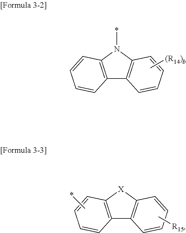


Applications Claiming Priority (2)
| Application Number | Priority Date | Filing Date | Title |
|---|---|---|---|
| KR1020180172141A KR102702683B1 (en) | 2018-12-28 | 2018-12-28 | Organic light emitting diode and organic light emitting device including the same |
| KR10-2018-0172141 | 2018-12-28 |
Publications (2)
| Publication Number | Publication Date |
|---|---|
| US20200212312A1 US20200212312A1 (en) | 2020-07-02 |
| US11380853B2 true US11380853B2 (en) | 2022-07-05 |
Family
ID=69005214
Family Applications (1)
| Application Number | Title | Priority Date | Filing Date |
|---|---|---|---|
| US16/725,917 Active 2040-12-08 US11380853B2 (en) | 2018-12-28 | 2019-12-23 | Organic light emitting diode and organic light emitting device including the same |
Country Status (4)
| Country | Link |
|---|---|
| US (1) | US11380853B2 (en) |
| EP (1) | EP3675193B1 (en) |
| KR (1) | KR102702683B1 (en) |
| CN (1) | CN111509132B (en) |
Families Citing this family (22)
| Publication number | Priority date | Publication date | Assignee | Title |
|---|---|---|---|---|
| US20240284786A1 (en) * | 2020-04-01 | 2024-08-22 | Idemitsu Kosan Co.,Ltd. | Organic electroluminescent element, compound, and electronic equipment |
| KR20220013910A (en) * | 2020-07-27 | 2022-02-04 | 엘티소재주식회사 | Heterocyclic compound, and organic light emitting device comprising same |
| KR102889905B1 (en) * | 2020-09-28 | 2025-11-21 | 엘지디스플레이 주식회사 | Organic light emitting diode and organic light emitting device including the same |
| KR102469770B1 (en) * | 2020-10-30 | 2022-11-23 | 엘티소재주식회사 | Heterocyclic compound, organic light emitting device comprising the same, manufacturing method of the same and composition for organic layer of organic light emitting device |
| WO2022092625A1 (en) * | 2020-10-30 | 2022-05-05 | 엘티소재주식회사 | Heterocyclic compound, organic light-emitting device comprising same, composition for organic layer of organic light-emitting device, and method for manufacturing organic light-emitting device |
| WO2022120773A1 (en) | 2020-12-11 | 2022-06-16 | 京东方科技集团股份有限公司 | Organic light emitting device and display apparatus |
| KR20220087116A (en) * | 2020-12-17 | 2022-06-24 | 엘지디스플레이 주식회사 | Organometallic compound, organic light emitting diode and organic light emitting device including the organometallic compound |
| KR102855865B1 (en) | 2020-12-21 | 2025-09-04 | 엘지디스플레이 주식회사 | Organic light emitting diode and Organic light emitting device including the same |
| KR102939101B1 (en) | 2020-12-29 | 2026-03-13 | 엘지디스플레이 주식회사 | Organic light emitting diode and organic light emitting device including the same |
| KR20220094636A (en) | 2020-12-29 | 2022-07-06 | 엘지디스플레이 주식회사 | Organic light emitting diode and organic light emitting device including the same |
| KR102917955B1 (en) * | 2021-01-04 | 2026-01-26 | 삼성디스플레이 주식회사 | Light emitting device and electronic apparatus including the device |
| CN112993199B (en) * | 2021-02-25 | 2023-03-07 | 上海弗屈尔光电科技有限公司 | A ternary composition, organic light-emitting element containing the composition and application |
| CN115260242B (en) * | 2021-04-29 | 2025-10-31 | 北京夏禾科技有限公司 | Organic electroluminescent material and device thereof |
| KR102726711B1 (en) * | 2021-05-11 | 2024-11-07 | 엘티소재주식회사 | Heterocyclic compound, organic light emitting device comprising same, and composition for organic layer of organic light emitting device |
| KR102917569B1 (en) * | 2021-11-26 | 2026-01-23 | 엘지디스플레이 주식회사 | Organic light emitting diode and organic light emitting device having thereof |
| KR102917568B1 (en) * | 2021-11-26 | 2026-01-23 | 엘지디스플레이 주식회사 | Organic light emitting diode and organic light emitting device having thereof |
| KR102917567B1 (en) * | 2021-11-26 | 2026-01-23 | 엘지디스플레이 주식회사 | Organic light emitting diode and organic light emitting device having thereof |
| KR102888467B1 (en) * | 2021-12-31 | 2025-11-20 | 엘지디스플레이 주식회사 | Light Emitting Device and Light Emitting Display Device Using the Same |
| KR102900365B1 (en) * | 2021-12-31 | 2025-12-15 | 엘지디스플레이 주식회사 | Light Emitting Device and Light Emitting Display Device Using the Same |
| CN120419338A (en) * | 2022-12-26 | 2025-08-01 | 三星Sdi株式会社 | Composition for organic optoelectronic device, and display device |
| KR20240107980A (en) * | 2022-12-30 | 2024-07-09 | 엘지디스플레이 주식회사 | Organic light emitting display apparatus |
| KR20250011755A (en) * | 2023-07-12 | 2025-01-22 | 덕산네오룩스 주식회사 | An organic electronic element comprising compound for organic electronic element and an electronic device thereof |
Citations (7)
| Publication number | Priority date | Publication date | Assignee | Title |
|---|---|---|---|---|
| US6660410B2 (en) | 2000-03-27 | 2003-12-09 | Idemitsu Kosan Co., Ltd. | Organic electroluminescence element |
| US7651786B2 (en) | 2002-07-19 | 2010-01-26 | Idemitsu Kosan, Co., Ltd. | Organic electroluminescence device and organic light emitting medium |
| US20100078631A1 (en) | 2008-09-30 | 2010-04-01 | Sung Hoon Pieh | Organic light emitting diode display device |
| US20170213988A1 (en) * | 2015-07-27 | 2017-07-27 | Heesung Material Ltd. | Hetero-cyclic compound and organic light emitting device using the same |
| KR20180060696A (en) | 2016-11-29 | 2018-06-07 | 희성소재 (주) | Hetero-cyclic compound and organic light emitting device using the same |
| EP3336159A1 (en) | 2016-09-06 | 2018-06-20 | LG Chem, Ltd. | Organic light-emitting element |
| KR20180096444A (en) | 2017-02-21 | 2018-08-29 | 희성소재 (주) | Organic light emitting device |
Family Cites Families (5)
| Publication number | Priority date | Publication date | Assignee | Title |
|---|---|---|---|---|
| TW349178B (en) | 1994-11-15 | 1999-01-01 | Sharp Kk | A method for the correction of a defect in a liquid crystal display device |
| KR101429537B1 (en) * | 2011-07-11 | 2014-08-12 | 엘지디스플레이 주식회사 | Organic light emitting diodes |
| KR101754715B1 (en) * | 2014-04-08 | 2017-07-10 | 롬엔드하스전자재료코리아유한회사 | Multi-component host material and organic electroluminescence device comprising the same |
| KR102463518B1 (en) * | 2014-12-08 | 2022-11-04 | 엘지디스플레이 주식회사 | Organic light emitting display device |
| TWI688137B (en) * | 2015-03-24 | 2020-03-11 | 學校法人關西學院 | Organic electric field light-emitting element, display device and lighting device |
-
2018
- 2018-12-28 KR KR1020180172141A patent/KR102702683B1/en active Active
-
2019
- 2019-12-19 EP EP19218119.6A patent/EP3675193B1/en active Active
- 2019-12-23 US US16/725,917 patent/US11380853B2/en active Active
- 2019-12-24 CN CN201911348303.1A patent/CN111509132B/en active Active
Patent Citations (7)
| Publication number | Priority date | Publication date | Assignee | Title |
|---|---|---|---|---|
| US6660410B2 (en) | 2000-03-27 | 2003-12-09 | Idemitsu Kosan Co., Ltd. | Organic electroluminescence element |
| US7651786B2 (en) | 2002-07-19 | 2010-01-26 | Idemitsu Kosan, Co., Ltd. | Organic electroluminescence device and organic light emitting medium |
| US20100078631A1 (en) | 2008-09-30 | 2010-04-01 | Sung Hoon Pieh | Organic light emitting diode display device |
| US20170213988A1 (en) * | 2015-07-27 | 2017-07-27 | Heesung Material Ltd. | Hetero-cyclic compound and organic light emitting device using the same |
| EP3336159A1 (en) | 2016-09-06 | 2018-06-20 | LG Chem, Ltd. | Organic light-emitting element |
| KR20180060696A (en) | 2016-11-29 | 2018-06-07 | 희성소재 (주) | Hetero-cyclic compound and organic light emitting device using the same |
| KR20180096444A (en) | 2017-02-21 | 2018-08-29 | 희성소재 (주) | Organic light emitting device |
Also Published As
| Publication number | Publication date |
|---|---|
| US20200212312A1 (en) | 2020-07-02 |
| KR102702683B1 (en) | 2024-09-03 |
| CN111509132B (en) | 2023-07-14 |
| CN111509132A (en) | 2020-08-07 |
| EP3675193B1 (en) | 2022-07-20 |
| KR20200082020A (en) | 2020-07-08 |
| EP3675193A1 (en) | 2020-07-01 |
Similar Documents
| Publication | Publication Date | Title |
|---|---|---|
| US11380853B2 (en) | Organic light emitting diode and organic light emitting device including the same | |
| US8986853B2 (en) | Red phosphorescent composition and organic electroluminescent device using the same | |
| US11557731B2 (en) | Organic light emitting diode having n-type host with narrow band gap and organic light emitting display device including the same | |
| US10770662B2 (en) | Organic compound, organic light emitting diode and organic light emitting display device | |
| US20260026230A1 (en) | Organic light emitting diode and organic light emitting device having thereof | |
| US12516033B2 (en) | Organic compound, and organic light emitting diode and organic light emitting display device including the same | |
| US8263237B2 (en) | Red phosphorescent composition and organic electroluminescent device using the same | |
| US12022731B2 (en) | Space-through charge transfer compound, and organic light emitting diode and organic light emitting display device including the same | |
| US20200044157A1 (en) | Organic Emitting Compound, and Organic Light Emitting Diode and Organic Light Emitting Display Device Including the Same | |
| US11814374B2 (en) | Organic compound, and organic light emitting diode and organic light emitting display device including the same | |
| US11505557B2 (en) | Organic compound, and organic light emitting diode and organic light emitting display device including the same | |
| US12545833B2 (en) | Organic compound, organic light emitting diode, and organic light emitting display device including the same | |
| US20210408395A1 (en) | Organic compound and organic light emitting diode and organic light emitting display device including the same | |
| US20240287112A1 (en) | Organometallic compound and organic light-emitting diode including the same | |
| US12156465B2 (en) | Space-through charge transfer compound, and organic light emitting diode and organic light emitting display device including the same | |
| US12446458B2 (en) | Organometallic compound, organic light emitting diode and organic light emitting device including the organometallic compound | |
| US11802102B2 (en) | Organic compound, and organic light emitting diode and organic light emitting display device including the same | |
| US20240244868A1 (en) | Organic light emitting diode comprising organometallic compound and plurality of host materials | |
| US20240244864A1 (en) | Organometallic compound and organic light emitting diode comprising the same | |
| US20240244947A1 (en) | Organic light emitting diode comprising organometallic compound and plurality of host materials | |
| US20240244866A1 (en) | Organic light emitting diode comprising organometallic compound and plurality of host materials | |
| US20240244949A1 (en) | Organometallic compound and organic light emitting diode comprising the same | |
| US20240392184A1 (en) | Organometallic compound and organic light-emitting diode including the same | |
| US20240244948A1 (en) | Organometallic compound and organic light emitting diode comprising the same | |
| US20240260446A1 (en) | Organic light emitting device comprising organometallic compound and plurality of host materials |
Legal Events
| Date | Code | Title | Description |
|---|---|---|---|
| FEPP | Fee payment procedure |
Free format text: ENTITY STATUS SET TO UNDISCOUNTED (ORIGINAL EVENT CODE: BIG.); ENTITY STATUS OF PATENT OWNER: LARGE ENTITY |
|
| AS | Assignment |
Owner name: HEESUNG MATERIAL CO., LTD., KOREA, REPUBLIC OF Free format text: ASSIGNMENT OF ASSIGNORS INTEREST;ASSIGNORS:KANG, HYE-SEUNG;KIM, DO-HAN;KIM, WOO-SAM;AND OTHERS;SIGNING DATES FROM 20191203 TO 20191216;REEL/FRAME:051481/0331 Owner name: LG DISPLAY CO., LTD., KOREA, REPUBLIC OF Free format text: ASSIGNMENT OF ASSIGNORS INTEREST;ASSIGNORS:KANG, HYE-SEUNG;KIM, DO-HAN;KIM, WOO-SAM;AND OTHERS;SIGNING DATES FROM 20191203 TO 20191216;REEL/FRAME:051481/0331 |
|
| STPP | Information on status: patent application and granting procedure in general |
Free format text: DOCKETED NEW CASE - READY FOR EXAMINATION |
|
| STPP | Information on status: patent application and granting procedure in general |
Free format text: NOTICE OF ALLOWANCE MAILED -- APPLICATION RECEIVED IN OFFICE OF PUBLICATIONS |
|
| STPP | Information on status: patent application and granting procedure in general |
Free format text: AWAITING TC RESP., ISSUE FEE NOT PAID |
|
| STPP | Information on status: patent application and granting procedure in general |
Free format text: NOTICE OF ALLOWANCE MAILED -- APPLICATION RECEIVED IN OFFICE OF PUBLICATIONS |
|
| STPP | Information on status: patent application and granting procedure in general |
Free format text: PUBLICATIONS -- ISSUE FEE PAYMENT RECEIVED |
|
| STPP | Information on status: patent application and granting procedure in general |
Free format text: PUBLICATIONS -- ISSUE FEE PAYMENT VERIFIED |
|
| STCF | Information on status: patent grant |
Free format text: PATENTED CASE |
|
| MAFP | Maintenance fee payment |
Free format text: PAYMENT OF MAINTENANCE FEE, 4TH YEAR, LARGE ENTITY (ORIGINAL EVENT CODE: M1551); ENTITY STATUS OF PATENT OWNER: LARGE ENTITY Year of fee payment: 4 |