US11380852B2 - N-type dopants for efficient solar cells - Google Patents
N-type dopants for efficient solar cells Download PDFInfo
- Publication number
- US11380852B2 US11380852B2 US16/712,206 US201916712206A US11380852B2 US 11380852 B2 US11380852 B2 US 11380852B2 US 201916712206 A US201916712206 A US 201916712206A US 11380852 B2 US11380852 B2 US 11380852B2
- Authority
- US
- United States
- Prior art keywords
- organic
- organic compound
- tbd
- pcbm
- acceptor
- Prior art date
- Legal status (The legal status is an assumption and is not a legal conclusion. Google has not performed a legal analysis and makes no representation as to the accuracy of the status listed.)
- Active
Links
- AUOAHJYPANAFDL-UHFFFAOYSA-N CN1CN2CN=C12 Chemical compound CN1CN2CN=C12 AUOAHJYPANAFDL-UHFFFAOYSA-N 0.000 description 15
- 0 *N1CN2CN=C12 Chemical compound *N1CN2CN=C12 0.000 description 9
- UKSSCWJBVWXFOM-UHFFFAOYSA-N C(CCCCCN1CCCN2CCCN=C12)CCCCN1CCCN2CCCN=C12.C(CCCN1CCCN2CCCN=C12)CCN1CCCN2CCCN=C12.C(CCN1CCCN2CCCN=C12)CN1CCCN2CCCN=C12 Chemical compound C(CCCCCN1CCCN2CCCN=C12)CCCCN1CCCN2CCCN=C12.C(CCCN1CCCN2CCCN=C12)CCN1CCCN2CCCN=C12.C(CCN1CCCN2CCCN=C12)CN1CCCN2CCCN=C12 UKSSCWJBVWXFOM-UHFFFAOYSA-N 0.000 description 3
- RIPUTAHEHSOQGM-ZOHITMODSA-N CN1CCCCCN2CCCN=C12.CN1CCCCN2CCCN=C12.CN1CCCN2CCCCC/N=C/12.CN1CCCN2CCCCN=C12.CN1CCCN2CCCN=C12.CN1CCCN2CCN=C12.CN1CCCN2CN=C12.CN1CCN2CCCN=C12.CN1CN2CCCN=C12 Chemical compound CN1CCCCCN2CCCN=C12.CN1CCCCN2CCCN=C12.CN1CCCN2CCCCC/N=C/12.CN1CCCN2CCCCN=C12.CN1CCCN2CCCN=C12.CN1CCCN2CCN=C12.CN1CCCN2CN=C12.CN1CCN2CCCN=C12.CN1CN2CCCN=C12 RIPUTAHEHSOQGM-ZOHITMODSA-N 0.000 description 3
- NOXHRXWEAGURSZ-UHFFFAOYSA-N c1c(CCCCN2CCCN3CCCN=C23)cc(CCCCN2CCCN3CCCN=C23)cc1CCCCN1CCCN2CCCN=C12 Chemical compound c1c(CCCCN2CCCN3CCCN=C23)cc(CCCCN2CCCN3CCCN=C23)cc1CCCCN1CCCN2CCCN=C12 NOXHRXWEAGURSZ-UHFFFAOYSA-N 0.000 description 3
- ULCJHBKDBZLXGQ-UHFFFAOYSA-N C.C(CCCCCN1CCCN2CCCN=C12)CCCCN1CCCN2CCCN=C12.C1CN=C2NCCCN2C1.[NaH] Chemical compound C.C(CCCCCN1CCCN2CCCN=C12)CCCCN1CCCN2CCCN=C12.C1CN=C2NCCCN2C1.[NaH] ULCJHBKDBZLXGQ-UHFFFAOYSA-N 0.000 description 1
- GQHTUMJGOHRCHB-UHFFFAOYSA-N C1CCC2=NCCCN2CC1 Chemical compound C1CCC2=NCCCN2CC1 GQHTUMJGOHRCHB-UHFFFAOYSA-N 0.000 description 1
- INCNPTBRGSEQDD-UHFFFAOYSA-N C1CC[N+]2=C3N(C1)CCCN3CCC2.C1CN=C2NCCCN2C1.[NaH] Chemical compound C1CC[N+]2=C3N(C1)CCCN3CCC2.C1CN=C2NCCCN2C1.[NaH] INCNPTBRGSEQDD-UHFFFAOYSA-N 0.000 description 1
Images


Classifications
-
- H01L51/0072—
-
- C—CHEMISTRY; METALLURGY
- C07—ORGANIC CHEMISTRY
- C07D—HETEROCYCLIC COMPOUNDS
- C07D487/00—Heterocyclic compounds containing nitrogen atoms as the only ring hetero atoms in the condensed system, not provided for by groups C07D451/00 - C07D477/00
- C07D487/12—Heterocyclic compounds containing nitrogen atoms as the only ring hetero atoms in the condensed system, not provided for by groups C07D451/00 - C07D477/00 in which the condensed system contains three hetero rings
- C07D487/16—Peri-condensed systems
-
- B—PERFORMING OPERATIONS; TRANSPORTING
- B82—NANOTECHNOLOGY
- B82Y—SPECIFIC USES OR APPLICATIONS OF NANOSTRUCTURES; MEASUREMENT OR ANALYSIS OF NANOSTRUCTURES; MANUFACTURE OR TREATMENT OF NANOSTRUCTURES
- B82Y30/00—Nanotechnology for materials or surface science, e.g. nanocomposites
-
- C—CHEMISTRY; METALLURGY
- C07—ORGANIC CHEMISTRY
- C07D—HETEROCYCLIC COMPOUNDS
- C07D487/00—Heterocyclic compounds containing nitrogen atoms as the only ring hetero atoms in the condensed system, not provided for by groups C07D451/00 - C07D477/00
- C07D487/12—Heterocyclic compounds containing nitrogen atoms as the only ring hetero atoms in the condensed system, not provided for by groups C07D451/00 - C07D477/00 in which the condensed system contains three hetero rings
-
- H01L51/0047—
-
- H—ELECTRICITY
- H10—SEMICONDUCTOR DEVICES; ELECTRIC SOLID-STATE DEVICES NOT OTHERWISE PROVIDED FOR
- H10K—ORGANIC ELECTRIC SOLID-STATE DEVICES
- H10K30/00—Organic devices sensitive to infrared radiation, light, electromagnetic radiation of shorter wavelength or corpuscular radiation
- H10K30/30—Organic devices sensitive to infrared radiation, light, electromagnetic radiation of shorter wavelength or corpuscular radiation comprising bulk heterojunctions, e.g. interpenetrating networks of donor and acceptor material domains
-
- H—ELECTRICITY
- H10—SEMICONDUCTOR DEVICES; ELECTRIC SOLID-STATE DEVICES NOT OTHERWISE PROVIDED FOR
- H10K—ORGANIC ELECTRIC SOLID-STATE DEVICES
- H10K50/00—Organic light-emitting devices
- H10K50/10—OLEDs or polymer light-emitting diodes [PLED]
- H10K50/14—Carrier transporting layers
- H10K50/16—Electron transporting layers
- H10K50/165—Electron transporting layers comprising dopants
-
- H—ELECTRICITY
- H10—SEMICONDUCTOR DEVICES; ELECTRIC SOLID-STATE DEVICES NOT OTHERWISE PROVIDED FOR
- H10K—ORGANIC ELECTRIC SOLID-STATE DEVICES
- H10K85/00—Organic materials used in the body or electrodes of devices covered by this subclass
- H10K85/20—Carbon compounds, e.g. carbon nanotubes or fullerenes
- H10K85/211—Fullerenes, e.g. C60
- H10K85/215—Fullerenes, e.g. C60 comprising substituents, e.g. PCBM
-
- H—ELECTRICITY
- H10—SEMICONDUCTOR DEVICES; ELECTRIC SOLID-STATE DEVICES NOT OTHERWISE PROVIDED FOR
- H10K—ORGANIC ELECTRIC SOLID-STATE DEVICES
- H10K85/00—Organic materials used in the body or electrodes of devices covered by this subclass
- H10K85/60—Organic compounds having low molecular weight
- H10K85/649—Aromatic compounds comprising a hetero atom
- H10K85/657—Polycyclic condensed heteroaromatic hydrocarbons
- H10K85/6572—Polycyclic condensed heteroaromatic hydrocarbons comprising only nitrogen in the heteroaromatic polycondensed ring system, e.g. phenanthroline or carbazole
-
- H—ELECTRICITY
- H01—ELECTRIC ELEMENTS
- H01B—CABLES; CONDUCTORS; INSULATORS; SELECTION OF MATERIALS FOR THEIR CONDUCTIVE, INSULATING OR DIELECTRIC PROPERTIES
- H01B1/00—Conductors or conductive bodies characterised by the conductive materials; Selection of materials as conductors
- H01B1/04—Conductors or conductive bodies characterised by the conductive materials; Selection of materials as conductors mainly consisting of carbon-silicon compounds, carbon or silicon
-
- H01L51/4253—
-
- H—ELECTRICITY
- H10—SEMICONDUCTOR DEVICES; ELECTRIC SOLID-STATE DEVICES NOT OTHERWISE PROVIDED FOR
- H10K—ORGANIC ELECTRIC SOLID-STATE DEVICES
- H10K30/00—Organic devices sensitive to infrared radiation, light, electromagnetic radiation of shorter wavelength or corpuscular radiation
- H10K30/50—Photovoltaic [PV] devices
Definitions
- the present invention relates to n-type dopants for organic devices.
- composition of matter useful as a n-type dopant for organic devices reports on a composition of matter useful as a n-type dopant for organic devices.
- the composition of matter can be embodied in many ways including, but not limited to, the following.
- composition of matter including an organic compound of the structure:
- R is any substituted or non-substituted alkyl, alkenyl, alkynyl, aryl or alkoxy group.
- composition of matter of any of the preceding embodiments, wherein the organic compound is a dimer (x 2) wherein each end of the R is connected to one of the
- composition of matter of embodiment 5, wherein the organic compound is
- composition of matter of any of the embodiments 1-4, wherein the organic compound is a trimer (x 3) wherein each end of the R is connected to one of the
- composition of matter of any of the preceding embodiments 1-8 bonded to a phenyl-C 61 -butyric acid methyl ester (PCBM) or Poly ⁇ [N,N′-bis(2-octyldodecyl)-naphthalene-1,4,5,8-bis(dicarboximide)-2,6-diyl]-alt-5,5′-(2,2′-bithiophene) ⁇ (N2200) so as to n-type dope the PCBM or the N2200.
- PCBM phenyl-C 61 -butyric acid methyl ester
- composition of embodiment 1 bonded to a fullerene so as to form the compound
- a device comprising the organic compounds of any of the preceding embodiments, wherein the device is a light emitting device, a light absorbing device, a thermoelectric device, or a transistor.
- a device comprising:
- an organic transistor an organic light absorbing device, a hybrid solar cell device, a photodetector device, a thermoelectric device, or an organic light emitting device comprising an n-type dopant including an organic compound of the structure:
- R is any substituted or non-substituted alkyl, alkenyl, alkynyl, aryl or alkoxy group.
- the device of any of the embodiments 20-22 further comprising a light absorbing active region including the n-type dopant.
- composition and device fabricated and characterized herein include, but are not limited to, a series of novel 1,5,7-Triazabicyclo[4.4.0]dec-5-ene (TBD) derivatives as air-stable n-dopants for organic semiconductors.
- TBD 1,5,7-Triazabicyclo[4.4.0]dec-5-ene
- These compounds have a guanidine structure which works as an electron-dopant and a long alkyl chain at the 7-position which increases their boiling point and solubility. This structural feature makes the compounds highly efficient and non-volatile n-dopants. Adding these compounds in the electron transport layer (ETL) of methylammonium lead iodide based solar cells increases the conductivity of the ETL and the solar cell efficiency.
- ETL electron transport layer
- FIG. 1 illustrates chemical structures of example n-type dopants based on triazabicyclodecene.
- FIG. 2 Thermal Gravimetric Analysis (TGA) thermal curves for various dopants (iPr-TBD, Me-TBD, H-TBD (TBD), C 10 -TBD, and 2TBD-C 10 ) under nitrogen. The temperature at which 10% weight loss is observed is listed above each curve.
- TGA Thermal Gravimetric Analysis
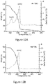
- FIG. 3A and FIG. 3B show cyclic voltammetry of C10-TBD and 2TBD-C10, wherein FIG. 3A shows potential (V) vs. Fc/Fc + and FIG. 3B shows potential (V) vs. Ag/Ag + .
- FIG. 4 Conductivities of doped PCBM films as a function of the molar ratio of TBD or DBU unit to PCBM.
- TBD-C10 has a data point only at 0.1 mol % since TBD-C10 doped PCBM solutions slipped off from quartz surface when the concentration was 1 or 10 mol %.
- TBD-EH data point at 10 mol % is also missing for the same reason.
- FIGS. 5A-5D Atomic Force Microscope (AFM) tomography images of PCBM films doped with 0.1 mol % ( FIG. 5A ), 1 mol % ( FIG. 5B ), 10 mol % of 2TBD-C10 ( FIG. 5C ); and a pristine PCBM film ( FIG. 5D ).
- AFM Atomic Force Microscope
- FIGS. 6A-6D 2-Dimensional grazing incident wide angle X-ray scattering (GIWAXS) images of pristine PCBM ( FIG. 6A ), PCBM with 10 mol % 2TBD-C10 ( FIG. 6B ), PCBM with 10 mol % Me-TBD ( FIG. 6C ), and PCBM with 10 mol % iPr-TBD ( FIG. 6D ).
- GIWAXS. 6A-6D 2-Dimensional grazing incident wide angle X-ray scattering
- FIG. 7 GIWAXS line cuts of undoped and doped PCBM films. Dashed lines are for eye guidance.
- FIGS. 8A-8C 2-Dimensional GIWAXS images of pristine N2200 ( FIG. 8A ), N2200 with 10 mol % 2TBD-C10 ( FIG. 8B ), and N2200 with 10 mol % TBD-C10 ( FIG. 8C ).
- FIGS. 9A-9B GIWAXS line cuts of undoped and doped P(NDI2OD-T2) films along in-plane ( FIG. 9A ) and out-of-plane ( FIG. 9B ) directions. Dashed lines are for eye guidance.
- FIG. 10A Current density-voltage (J-V) characteristics (current density in milliamps per centimeter square as a function of voltage between the cathode and anode) of a solar cell having a light absorbing region comprising methylammonium lead triiodide (MAPbI 3 ) and an electron transport layer (ETL) comprising PCBM doped with 2TBD-C10 in a ratio of (orange) 0.1 mol %, (green) 1 mol % and (purple) 10 mol %. Dashed lines represent forward scans, while solid lines reverse scans.
- Device structure is ITO/PTAA/MAPbI 3 /ETL (0-10% dopant)/Ag.
- FIG. 10B J-V characteristics of a perovskite solar cell having a light absorbing region comprising methylammonium lead triiodide (MAPbI 3 ) and an ETL comprising PCBM doped with 1% TBD-C10 or TBD-EH. Dashed lines represent forward scans, while solid lines reverse scans.
- Device structure is ITO/PTAA/MAPbI 3 /ETL (0-10% dopant)/Ag.
- FIG. 10C J-V characteristics of a solar cell having a light absorbing region comprising methylammonium lead triiodide (MAPbI 3 ) and an electron transport layer (ETL) comprising ITIC doped with Me-TBD (black 10 wt % MeTBD, yellow 1 wt % Me-TBD, and blue 0.1% wt % Me-TBD).
- MAbI 3 methylammonium lead triiodide
- ETL electron transport layer
- FIGS. 11A-11B compare performance of the guanidine-type n-type dopant in a solar cell (according to one or more embodiments) with performance of an amidine (DBU) type n-type dopant in a solar cell [6], showing ( FIG. 11B ) the guanidine based dopant successfully doped PCBM so that a solar cell including PCBM doped with guanidine as an electron transporting layer (ETL) has comparable short circuit current (I SC ) and fill factor (FF) as compared to the solar cell having a PCBM ETL doped with an amidine ( FIG. 11A , taken from 6 ).
- the structure of the measured devices in both cases is glass/ITO/PTAA/MAPbI 3 (400 nm)/PCBM+dopant (1 mol %)/Ag (100 nm).
- FIGS. 12A-12E TGA and first derivative curves of the dopants under nitrogen flow, for the dopant iPR-TBD ( FIG. 12A ), Me-TBD ( FIG. 12B ), TBD ( FIG. 12C ), C10-TBD ( FIG. 12D ), and 2TBD-C 10 ( FIG. 12E ).
- FIGS. 13A-13F Nuclear Magnetic Resonance (NMR) measurements of various triazabicyclodecene-based compounds including NMR of iPr-TBD in CDCl 3 ( FIG. 13A , 1 H NMR; FIG. 13B , 13 C NMR), C 10 -TBD in CDCl 3 ( FIG. 13C , 1 H NMR; FIG. 13D ; 13 C NMR), 2TBD-C10 in CDCl 3 ( FIG. 13E , 1 H NMR; FIG. 13F . 13 C NMR)
- FIG. 14 Flowchart illustrating a method of making an n-type dopant and/or device including the n-type dopant.
- FIG. 15 illustrates a solar cell or photodetector including an organic compound according to one or more embodiments described herein.
- FIG. 16 illustrates an organic light emitting diode (OLED) including an organic compound according to one or more embodiments described herein.
- OLED organic light emitting diode
- FIG. 17 illustrates an organic field effect transistor including an organic compound according to one or more embodiments described herein.
- FIG. 18 illustrates a thermoelectric device including an organic compound according to one or more embodiments described herein.
- FIG. 19 Schematic illustrating the operation of the n-type dopant.
- FIG. 1 illustrates a series of triazabicyclodecene-based compounds used as n-dopants with varying physical properties, namely TBD, iPr-TBD, Me-TBD, C10-TBD, 2TBD-C10.
- TBD triazabicyclodecene-based compounds
- iPr-TBD Me-TBD
- C10-TBD C10-TBD
- 2TBD-C10 introducing a variety of N-substituents enabled control of the volatility of the materials and whether they were solid or liquid. For example, doubling the ratio of TBD groups to alkyl chain in 2TBD-C10 gave a solid material with high thermal stability above 250° C. All the TBD n-dopants effectively increase the conductivity of PCBM films, with 2TBD-C10 achieving a high of 6.5 ⁇ 10 ⁇ 2 Siemens per centimeter (S/cm).
- 2TBD-C10 was also shown to effectively dope poly ⁇ [N,N′-bis(2-octyldodecyl)naphthalene-1,4,5,8-bis(dicarboximide)-2,6-diyl]-alt-5,5′-(2,2′-bithiophene) ⁇ (P(NDI2OD-T2), also called N2200) and 3,9-bis(2-methylene-(3-(1,1-dicyanomethylene)-indanone))-5,5,11, l-tetrakis(4-hexylphenyl)-dithieno[2,3-d:2′,3′-d′]-s-indaceno[1,2-b:5,6-b′]dithiophene (ITIC).
- PCBM doped by 2TBD-C10 led to improved fill factors and PCEs.
- guanidine-type dopants described herein are effective electron donors due to the three nitrogen atoms that stabilize the central carbocation.
- the following sections report on the effectiveness of these TBD molecules as n-dopants, the effect substituents have on the physical properties, thermal stability, and resulting performance of these materials.
- TBD 1,5,7-Triazabicyclo[4.4.0]dec-5-ene
- Me-TBD 7-methyl-1,5,7-triazabicyclo[4.4.0]dec-5-ene
- Me-TBD 7-methyl-1,5,7-triazabicyclo[4.4.0]dec-5-ene
- Me-TBD 7-methyl-1,5,7-triazabicyclo[4.4.0]dec-5-ene
- Me-TBD 7-methyl-1,5,7-triazabicyclo[4.4.0]dec-5-ene
- 2TBD-C10 on the other hand, with double the TBD moiety ratio to alkyl chain, is a white powdery solid. All the dopants are readily soluble in both polar and non-polar organic solvents, as well as water and methanol. This allows for versatile processing, employing either blends or sequential applications with anti-solvents.
- the advantages of this synthetic method and products include one pot synthesis, air stable products, and control volatility/greasiness with the choice of alkyl group. Moreover, the product can be both water and organic soluble which allows for blend or sequential processing in device fabrication.
- TBD-C 60 The synthesis of TBD-C 60 is as follows.
- TBD-C 60 dyad was synthesized in two steps following the scheme above. Covalently attaching TBD to PCBM can reduce the phase separation of the TBD when the TBD is blended with the fullerene-based acceptors. Surprisingly, the product is very insoluble in various solvents, which indicates that the TBD may be already self-doped at room temperature with the TBD unit as the electron donor and the fullerene cage as the electron acceptor (due to the close proximity of the two units).
- TBD-Cylic-C4 The synthesis of TBD-Cylic-C4 was as follows.
- TBD thermal gravimetric analysis
- the TBD moiety In order to act as efficient n-dopants, the TBD moiety must be readily oxidized. We used cyclic voltammetry to compare the oxidation potentials of C10-TBD and 2TBD-C10 ( FIG. 3 ). Both dopants showed highly irreversible oxidation potentials, C10-TBD at 1.00 V and 2TBD-C10 at 1.05 V. This close match signifies that in 2TBD-C10, the two tethered TBD moieties are behaving independently. Versus a ferrocene internal standard, this represents Highest Unoccupied Molecular Orbital (HOMO) levels of about ⁇ 5.1 eV for both dopants. The ability of these materials to n-dope PCBM with a Lowest Unoccupied Molecular Orbital (LUMO) level ca. ⁇ 4.0 eV is indication of a stable, favored charged byproduct or the formation of an intermediate reducing species.
- HOMO Highest Unoccupied Molecular Orbital
- In-plane conductivities of doped PCBM films indicate that, among the TBD, DBU, and TBD derivatives synthesized herein, 2TBD-C10 gives the best conductivity throughout the 0.1 to 10 mol % doping ratio range ( FIG. 4 , Table 1).
- the conductivities of the films are 1.8 ⁇ 10 ⁇ 4 , 3.5 ⁇ 10 ⁇ 3 , and 6.5 ⁇ 10 ⁇ 2 S/cm with 0.1, 1, and 10 mol % TBD unit ratio to PCBM, respectively.
- the trend fits well to a simple power law (y y 0 +Ax ⁇ ) with ⁇ of 1.27.
- PCBM films doped by 2TBD-C10 are more tolerant to thermal annealing than those doped with TBDs with short side chains, due to increased boiling point and thermal stability.
- the conductivity of the 1 mol % 2TBD-C10 doped PCBM film increased from 3.5 ⁇ 10 ⁇ 3 to 7.4 ⁇ 10 ⁇ 3 S/cm after thermal annealing on a hot plate in nitrogen at 150° C. for 30 min, whereas that of Me-TBD doped film's conductivity dropped from 6.2 ⁇ 10 ⁇ 4 to 5.6 ⁇ 10 ⁇ 5 S/cm under the same treatment.
- Better thermal tolerance is advantageous since it can expand thermal parameters in fabrication processes and enhance stability during operation in increased temperature.
- 2TBD-C10 efficiently dopes other “n-type” organic semiconductors as well.
- a film comprising P(NDI2OD-T2), a well-studied naphthalenediimide based conjugated polymer with high mobility, [6] doped with 2TBD-C10 has a conductivity of 7.0 k 10 ⁇ 4 S/cm with 10 mol % TBD unit (Table 2). This value is comparable with P(NDI2OD-T2) doped with (2-Cyc-DMBI) 2 (2.8 ⁇ 10 ⁇ 3 S/cm with 11 mol %) [4] and P(NDI2OD-T2) doped with N-DMBI (8 ⁇ 10 ⁇ 4 S/cm with 10 mol %).
- P(NDI2OD-T2) doped with TBD-C10 has three order of magnitude lower conductivity (1.5 ⁇ 10 ⁇ 7 S/cm) in 10 mol % doping.
- 2TBD-C10 also dopes ITIC, an acceptor-donor-acceptor type non-fullerene acceptor for organic photovoltaics, yielding conductivities of 4.3 ⁇ 10 ⁇ 6 and 1.7 ⁇ 10 ⁇ 6 S/cm with 10 and 1 mol % doping, respectively.
- These relatively low conductivities are partly due to lower mobility of ITIC ( ⁇ 10 4 cm 2 Ns at space-charged limit current (SCLC)) [8] than that of PCBM (3 ⁇ 10 ⁇ 3 cm 2 /Vs at SCLC).
- the scattering patterns of P(NDI2OD-T2) are also insensitive to doping with 2TBD-C10 and TBD-C10 ( FIG. 8 (2D) and 9(line cut)).
- the scattering pattern of pristine P(NDI2OD-T2) show a ⁇ -staking feature at 1.6 ⁇ ⁇ 1 in the out-of-plane direction and alkyl stacking features at 0.25 and 0.47 ⁇ ⁇ 1 in the in-plane direction, indicating a face-on orientation of its crystalline moieties.
- Addition of 2TBD-10 or TBD-C10 does not result in a notable shift of the polymer originated peaks or appearance of new peaks.
- PCE photovoltaic conversion efficiency
- V OC open circuit voltage
- J SC short circuit current
- TBD-C10, TBD-EH doped PCBM and Me-TBD doped ITIC work well as an ETL in perovskite solar cells as well.
- Improved device J SC , FF and PCE were achieved with optimized dopant concentration (Table 3 and FIG. 10B, 10C ).
- FIG. 11B shows the guanidine based dopant TBD and Me-TBD successfully doped PCBM so that a solar cell including the PCBM doped with guanidine as an electron transporting layer (ETL) has increased short circuit current (I SC ) and fill factor (FF) as compared to the solar cell having a PCBM ETL doped with an amidine ( FIG. 11A , taken from 6 )
- ETL electron transporting layer
- FF fill factor
- TBD 1,5,7-Triazabicyclo[4.4.0]dec-5-ene
- Me-TBD 7-methyl-1,5,7-triazabicyclo[4.4.0]dec-5-ene
- All manipulations involving air-sensitive reagents were performed under an atmosphere of dry argon.
- 1 H and 13 C NMR spectra were recorded on a Varian Inova600 spectrometer.
- Thermal gravimetric analysis was performed on a TA Discovery TGA under nitrogen.
- the mass spectroscopic data were obtained at the UCSB mass spectrometry facility on a Waters Micromass LCT Premier mass spectrometer operating in W mode, using polyethylene glycol as an internal standard.
- Electrochemical measurements were carried out in 0.1 M tetrabutylammonium hexafluorophosphate in dry, degassed dichloromethane with platinum wires as the working and counter electrodes and silver wire as a pseudo-reference electrode.
- a ferrocene-ferrocenium (Fc/Fc+) redox couple was used as an internal standard and its redox potential assumed to be ⁇ 4.80 eV below vacuum level.
- 2TBD-C10 Dry THF (50 mL) was loaded into a flame-dried 250 ml schlenk flask under argon, followed by NaH (0.115 g, 4.90 mmol) and 1,5,7-triazabicyclo[4.4.0]dec-5-ene (TBD, 0.507 g, 3.59 mmol). The reaction mixture was stirred for 4 hours, after which was added 1,10-dibromodecane (0.489 g, 1.63 mmol) under positive pressure. The reaction was stirred at room temperature overnight under argon. The slightly turbid, fawn colored reaction mixture was filtered and rinsed with DCM. The filtrate was reduced in vacuo to afford a white, waxy solid.
- the product was purified by trituration by dissolving the product in small amounts of hexane (3 ⁇ 5 mL), decanting and combining the fractions. The solvent was removed in vacuo to afford 2TBD-C10 as a white powdery solid (0.591 g, 88% yield).
- iPr-TBD Using a similar procedure as described above, NaH (0.133 g, 5.56 mmol), TBD (0.516 g, 3.71 mmol), and 2-bromopropane (1.04 mL, 11.1 mmol) were reacted to afford a yellow oil. The product was triturated with small amounts of THF or methyl tert-butyl ether (5 ⁇ 2 mL), decanting and combining the fractions. The solvent was removed in vacuo to afford iPr-TBD as a viscous, yellow oil (0.183 g, 27% yield).
- the product was purified by dissolving it in hexane (25 mL) and washing thoroughly with water (3 ⁇ 25 mL) to remove unreacted TBD. The organic fraction was dried over Na 2 SO 4 , filtered, and reduced in vacuo to afford C10-TBD as a light yellow oil (0.338 g, 78% yield).
- Thin film samples were deposited on quartz substrates by spin-coating in a N2-filled globe box (O 2 and water concentrations were below 0.1 parts per million (ppm)). Before spin-coating, the substrates were washed with detergent, deionized water, acetone, and isopropylalcohol in a sonication bath, then treated with air-plasma under 300 mbar for 10 min.
- Organic semiconductor (OS) and dopant were dissolved in chlorobenzene at 20 mM. Dopant solutions of 2 mM and 0.2 mM were also prepared by diluting the 20 mM solutions. OS solutions were stirred at 60-75° C.
- PTFE polytetrafluoroethylene
- a OS solution and a dopant solution were mixed at a ratio of 10:1 to obtain a 0.1, 1.0 or 10 mol % doped OS solution.
- the doped solutions were spin-coated at 1000 rpm for 30 s within 30 min after mixture without heating.
- P(NDI2OD-T2) films were annealed on a hot plate at 150° C. for 60 min under nitrogen. PCBM films were not annealed. The film thicknesses measured with a profilometer (Dektak XT) and they were 30-80 nm.
- Gold electrical contact with a thickness of 80 nm was thermally evaporated onto the films though a shadow mask.
- Each channel has four electrode bars of 10 mm width. The distances of the bars from the side bar were 0.2, 0.5, and 0.8 mm.
- In-plane conductivity were measured by Keithley 6487 Picoammeter with the two-point probe method. Resistances were measured with three distances and plotted against distance/width. The sheet resistance was obtained by the least-square fit of the linear trend. The conductivity was then calculated by dividing the sheet resistance by the thickness.
- Grazing incidence X-ray scattering experiments were conducted at the Advanced Light Source at beamline 7.3.3.
- the energy of the incident beam was at 10 keV, and a Pilatus 2 M area detector was used.
- the X-ray scattering data were taken at incidence angles of 0.15° with 2-30 s exposure times.
- the samples were kept under helium environment during X-ray exposure to minimize air scattering and sample degradation.
- the collected data were processed using Nika, a 2D data reduction macro on Igor Pro (WaveMetrics) using established procedures.
- a diffraction pattern from silver behenate was used to calibrate the beam center and the sample-to-detector distance.
- ITO Indium Tin Oxide
- PTAA polytriarylamine
- Aldrich chlorobenzene
- a MAPbI 3 precursor solution was formulated by dissolving a 1/1/1 (mol/mol/mol) mixture of methylammonium iodide (Dysol), lead iodide (Aldrich) and dimethyl sulfide (Aldrich) in anhydrous DMF (Aldrich).
- the DMF solution was spun coat on the PTAA layer at 1000 rpm for 10 s then 4000 rpm for 30 s.
- 0.2 mL of anhydrous chlorobenzene (Aldrich) was dropped on the substrate.
- the films were transferred on a hotplate of 100° C. immediately, and thermally annealed for 10 min.
- a solution for the ETL layer (30 mg/mL PCBM with 0-10% of dopants in chlorobenzene) were spun coat on the MAPbI 3 layer at 1000 rpm, optionally followed by a spin-coat of PEIE in isopropyl alcohol (0.02 wt %, diluted from 37% aqueous solution of PEIE from Aldrich) at 6000 rpm.
- the devices were finally capped with Ag (80 nm) by vacuum deposition.
- the J-V characteristics were measured at 1 sun illumination (AM 1.5G, 100 mW/cm 2 ) in a N 2 -filled glovebox with a solar simulator equipped with a Xenon lamp (Newport), a Keithley 2602 Source Meter and a calibrated silicon reference cell.
- the voltage was ramped from 1.50 V to ⁇ 0.50 V then back to 1.50 V with 0.01 V step and 0.03 s delay time.
- FIG. 14 is a flowchart illustrating a method of making a dopant and/or a device including the dopant.
- Block 1400 represents obtaining a compound comprising a guanidine of the structure:
- Block 1402 represents combining the compound comprising guanidine with a carbon containing organic compound R, so as to form a composition of matter of the structure:
- R is any substituted or non-substituted alkyl, alkenyl, alkynyl, aryl or alkoxy group.
- R is ⁇ C 2 H 2 ⁇ , —C 2 H 3 ⁇ , —C 2 H 4 —, —C 2 H 5 , ⁇ C 3 H 4 ⁇ , —C 3 H 5 ⁇ , —C 3 H 6 —, —C 3 H 7 , ⁇ C 4 H 6 ⁇ , —C 4 H 7 ⁇ , —C 4 H 5 —, —C 4 H 9 , ⁇ C 5 H 5 ⁇ , —C 5 H 9 ⁇ , —C 5 H 10 —, —C 5 H 11 , ⁇ C 6 H 10 ⁇ , —C 6 H 11 ⁇ , —C 6 H 12 —, —C 6 H 13 , ⁇ C 7 H 12 ⁇ , —C 7 H 13 ⁇ , —C 7 H 14 —, —C 7 H 15 , ⁇ C 8 H 14 ⁇ , —C 5 H 15 ⁇ , —C 8 H 16 —, —C 8 H 17 ,
- Block 1404 represents optionally combining an acceptor with the composition of matter.
- Block 1406 represents optionally solution processing the acceptor and/or composition of matter so as to form a device, such as, but not limited to, an organic solar cell, a hybrid solar cell, an organic field-effect transistor, an organic light-emitting diode, an organic photodetector or a hybrid photodetector.
- a device such as, but not limited to, an organic solar cell, a hybrid solar cell, an organic field-effect transistor, an organic light-emitting diode, an organic photodetector or a hybrid photodetector.
- FIG. 15 illustrates an example device 1500 comprising a solar cell or photodetector comprising an (e.g., transparent) anode 1502 ; an anode interface layer 1504 ; an absorbing active region 1506 (e.g., comprising organic semiconductor blends or perovskite) on the anode interface layer 1504 ; a cathode interface layer or electron transport layer 1508 (e.g., comprising an electron acceptor with TBD dopant) on the absorbing active region 1506 ; and a cathode 1510 on the cathode interface layer 1508 .
- Cathode 1510 or anode 1502 can be on a substrate 1512 .
- FIG. 16 illustrates and example organic light emitting device 1600 comprising an (e.g., transparent) anode 1602 ; an anode interface layer 1604 ; an electromagnetic radiation emitting active region 1606 (e.g., comprising organic semiconductor blends) on the anode interface layer 1604 ; a cathode interface layer or electron transport layer 1608 (e.g., comprising an electron acceptor with TBD dopant) on the active region 1606 ; and a cathode 1610 on the cathode interface layer 1608 .
- Cathode 1610 or anode 1602 can be on a substrate 1612 .
- FIG. 17 illustrates and example organic transistor device 1700 comprising a channel region 1702 including the organic compound according to embodiments described herein; a source contact S to the channel region 1702 ; a drain contact D to the channel region 1702 ; a gate contact G; and a dielectric 1704 between the channel region 1702 and the gate contact G, wherein an electric field applied between the gate contact and the source contact or the drain contact modulates flow of current in the channel region between the source contact and the drain contact.
- the device is on a substrate 1706 .
- FIG. 18 illustrates an example thermoelectric device 1800 comprising an n-type region 1802 (comprising an organic compound as described herein) and p-type region between two metal layers 1804 .
- the device 1800 operates in power generation mode when a load is connected to the device and a heat source is thermally coupled to one of the metal layers and a heat sink is thermally coupled to another of the metal layers.
- the device operates as a refrigerator when a bias is applied across the device.
- perovskite refers to a material with a three-dimensional crystal structure related to that of CaTiO 3 or a material comprising a layer of material, wherein the layer has a structure related to that of CaTiO 3 .
- the perovskite structure can be represented by the formula AMX 3 , wherein A and M are cations of different sizes, typically A having a charge of +1 and 1M having a charge of +2 and X is an anion (charge ⁇ 1).
- A, M and X are varied, the different ion sizes may cause the structure of the perovskite material to distort away from the highly symmetric cubic structure adopted by CaTiO 3 to a lower-symmetry distorted structure.
- a perovskite material can be represented by the formula AMX 3 , wherein A is at least one cation, M is at least one cation and X is at least one anion.
- A is at least one cation
- M is at least one cation
- X is at least one anion.
- the perovskite comprises more than one A cation
- the different A cations may be distributed over the A sites in an ordered or disordered way.
- the perovskite comprises more than one M cation
- the different M cations may be distributed over the M sites in an ordered or disordered way.
- the perovskite may comprise a first cation, a second cation, and at least one anion.
- the perovskite may comprise further cations or further anions.
- the perovskite may comprise two, three or four different first cations; two, three or four different second cations; and two, three or four different anions.
- A is at least one organic or inorganic cation, which may be selected from the group consisting of H + , H 3 O + , NH 4 + , H 3 NOH + , Li + , Na + , K + , Rb + , Cs + , Cu + , Tl + , Ag + , BiO + , methylammonium CH 3 NH 3 + , ethylammonium (C 2 H 5 )NH 3 + , alkylammonium, formamidinium NH 2 (CH)NH 2 + , guanidinium C(NH 2 ) 3 + , imidazolium C 3 N 2 H 5 + , hydrazinium H 2 N—NH 3 + , azetidinium (CH 2 ) 3 NH 2 + , dimethylammonium (CH 3 ) 2 NH 2 + , tetramethylammonium (CH 3 ) 4 N + , phenylammonium C 6
- M is at least one divalent metal cation, which may be selected from the group consisting of Ca 2+ , Sr 2+ , Cd 2+ , Cu 2+ , Ni 2+ , Mn 2+ , Fe 2+ , Co 2+ , Pd 2 ⁇ , Ge 2+ , Sn 2 ⁇ , Pb 2 ⁇ , Hg 2+ , Yb 2+ and Eu 2+ ; in one or more embodiments, M is preferably Pb 2+ or Sn 2+ ; X is a monovalent anion, including but not limited to a halide anion F ⁇ , Cl ⁇ , Br ⁇ , I ⁇ , a cyanide CN ⁇ , or a formate HCOO ⁇ ; X can be a single kind of anion, or comprise two, three of four different kinds of anions.
- B is a divalent primary, secondary, tertiary, or quaternary organic ammonium cation with 1 to 100 carbons and 2 to 30 heteroatoms, wherein two of the heteroatoms are positively charged nitrogen atoms.
- B is selected from the group consisting of Mg 2+ , Ca 2+, Sr 2+ , Ba 2+ , Sn 2+ , Ti 2+ , V 2+ , Ni 2+ , Cr 2+ , Co 2+ , Fe 2+ , Cu 2+ , Zn 2+ , Mn 2+ , Hg 2+ , Ag 2+ , NH 3 CH 2 CH 2 NH 3 2+ , NH 3 (CH 2 ) 6 NH 3 2+ , NH 3 (CH 2 )NH 3 2+ , and NH 3 C 6 H 4 NH 3 2+
- the active layer may comprise a material selected from the group consisting of MX 3 , AMX 4 , A 3 AX 4 , A 3 M 2 X, perovskites, A 2 MM′X 6 double perovskites, and A n+1 A′ n/2 M n/2 X 3n+1 Ruddlesden-Popper phases, wherein A represents a monovalent inorganic cation, a monovalent organic cation; A′represents a second monovalent organic or inorganic cation; M is Bi 3+ or Sb 3+ ; X represents a monovalent halide anion, or mixture of different monovalent halide anions.
- double perovskite refers to a compound which is closely related to the perovskite AMX 3 compound but has a unit cell twice that of perovskite and two different metals on the M sites, so the formula can be written as A 2 MM′X 6 .
- the term “Ruddlesden-Popper phase” as used herein refers to a form of layered perovskite structures which consist of two-dimensional perovskite slabs and additional cation interlayers. The general formula of those phases can be written as A n+1 A′ n/2 M n/2 X 3n+1 .
- the active layer is a bismuth halide selected from the group consisting of BiI 3 , K 3 Bi 2 I 9 , Rb 3 Bi 2 I 9 , Cs 3 Bi 2 I 9 , (CH 3 NH 3 ) 3 Bi 2 I 9 , (NH 2 (CH)NH 2 ) 3 Bi 2 I 9 , and (NH 3 (CH 2 ) 2 NH 3 ) 2 Bi 2 I 10 .
- the perovskite photovoltaic device may have a standard or inverted structure. It may comprise a substrate, a first electrode deposited on the substrate, a second electrode, an electron conducting/hole blocking layer deposited either between the first electrode and the active layer, or between the active layer and the second electrode, and an optional hole conducting/electron blocking layer deposited either in between the first electrode and the active layer, or between the active layer and the second electrode.
- both the electron donor and the electron acceptor absorb photons to create electron-hole pairs
- the (acceptor molecule interfacing with the donor molecule) receives the electron in the electron hole pair and transports the electron to the cathode interface layer and the cathode.
- the hole is transported by the donor to the anode interface layer and then the anode.
- the electron transporting/conducting layer material can be selected from, but not limited to, the group comprising or consisting of TiO 2 , ZnO, SnO 2 , SiO 2 , ZrO 2 , CdSe, WO 3 , ZnSnO 4 , PbI 2 , SrTiO 3 , fullerene based electron acceptors (C 60 , C 70 , PC 61 BM, PC 71 BM, ICBA), borane based electron acceptors (3TPYMB), Bathocuproine (BCP), bathophenanthroline (Bphen), ITIC type of non-fullerene acceptors, NDI and PDI based non-fullerene acceptors, and the combination of above (double layer).
- the group comprising or consisting of TiO 2 , ZnO, SnO 2 , SiO 2 , ZrO 2 , CdSe, WO 3 , ZnSnO 4 , PbI 2
- the electron transporting layer may have a thickness of 2 nm to 500 nm, preferably a thickness of 20 nm to 200 nm, more preferably a thickness of 50 nm to 100 nm.
- the hole transporting/conducting layer material can be selected from, but not limited to, the group comprising or consisting of poly(3,4-ethylenedioxythiophene): polystyrene sulfonate (PEDOT:PSS), p-type organic small molecule semiconductors such as Spiro-MeOTAD, pentacene, biscarbazolylbenzene, oligomer semiconductors, polymer semiconductors such as PTAA, poly(3-hexylthiophene-2,5-diyl) (P3HT), donor-acceptor copolymer semiconductors such as PCPDTBT, PCDTBT, metal oxides such as Cul, CuBr, CuSCN, Cu 2 O, CuO or CIS.
- PDOT polystyrene sulfonate
- P3HT poly(3-hexylthiophene-2,5-diyl)
- PCPDTBT poly(3-hexylthiophene-2,5-d
- the active layer, electron transporting/hole blocking layers, hole transporting/electron blocking layers of the electronic device may be deposited by solution casting or vapor deposition.
- Illustrative thin film deposition methods include a spin coating method, a casting method, a microgravure coating method, a gravure coating method, a bar coating method, a roll coating method, a blade coating method, a wire bar coating method, a dip coating method, a spray coating method, a free span coating method, a dye coating method, a screen printing method, a flexo printing method, an offset printing method, an inkjet printing method, a dispenser printing method, a nozzle coating method and a capillary coating method, for forming a film from a solution.
- the solar cell has a fill factor of more than 70%, an J SC over 19 mA/cm 2 , and a PCE of greater than 14%.
- composition of matter and/or device can be embodied in many ways including, but not limited to, the following.
- composition of matter comprising:
- R is any substituted or non-substituted alkyl, alkenyl, alkynyl, aryl or alkoxy group.
- composition of matter of embodiment 1, wherein R contains one or more heteroatoms e.g., selected from the group comprising, but not limited to, silicon, oxygen, nitrogen, phosphorus sulfur and halides).
- composition of matter of embodiments 1 or 2, wherein R contains one or more aromatic moieties e.g., comprising, but not limited to benzene or benzene derivatives, thiophene or thiophene derivatives).
- composition of matter of any of the preceding embodiments, wherein the organic compound is a dimer (x 2) wherein each end of the R is connected to one of the
- composition of matter of embodiment 5, wherein the organic compound is
- composition of matter of any of the embodiments 1-4, wherein the organic compound is a trimer (x 3) wherein each end of the R is connected to one of the
- composition of matter of any of the preceding embodiments 1-8 bonded to a compound such as, but not limited to, a phenyl-C 61 -butyric acid methyl ester (PCBM), Poly ⁇ [N,N′-bis(2-octyldodecyl)-naphthalene-1,4,5,8-bis(dicarboximide)-2,6-diyl]-alt-5,5′-(2,2′-bithiophene) ⁇ (N2200) any fullerene acceptor as described in [12], any non-fullerene acceptor described in [13], the compound having mostly planar pi-conjugated core with donor and acceptor building blocks, or a material having an electron affinity of 3-5 electron volts (eV) or 3-4.5 eV, so as to n-type dope the compound.
- a compound such as, but not limited to, a phenyl-C 61 -butyric acid methyl ester (PCBM), Poly
- composition of matter of any of the preceding embodiments 1-8 bonded to an electron acceptor (e.g., comprising a second organic compound) so as to n-type dope the electron acceptor.
- the second organic compound include, but are not limited to, a fullerene (including any fullerene acceptor described in [12], PCBM, N 2200 , ITIC, any non-fullerene acceptor described in [13], a compound having mostly planar pi-conjugated core with donor and acceptor building blocks, or a material having an electron affinity of 3-5 eV or 3-4.5 eV.
- composition of matter of embodiment 1 bonded to a fullerene, or wherein the R comprises the fullerene, so as to form the composition of matter comprising or compound having the structure:
- organic acceptor include, but are not limited to, a fullerene, PCBM, N2200 or ITIC.
- a device comprising the organic compounds or composition of matter of any of the embodiments 1-14, wherein the device is a light emitting device (e.g., as illustrated in FIG. 16 ), a light absorbing device (e.g., as illustrated in FIG. 15 ), a thermoelectric device (as illustrated in FIG. 18 and comprising an n-type region including the organic compound of any of the examples 1-14), or a transistor (e.g., as illustrated in FIG. 17 ).
- a light emitting device e.g., as illustrated in FIG. 16
- a light absorbing device e.g., as illustrated in FIG. 15
- a thermoelectric device as illustrated in FIG. 18 and comprising an n-type region including the organic compound of any of the examples 1-14
- a transistor e.g., as illustrated in FIG. 17
- an active region including but not limited to an perovskite
- electron transporting layer e.g., PCBM, ITIC, N2200
- the organic compound is n-type self-doped such that the organic compound emits light in response to current (e.g., when the active region 1606 comprises the organic compound of any of the embodiments 1-14), transports current in a channel of a transistor (e.g., when the channel region 1702 comprises the organic compound of any of the embodiments 1-14), or generates current in response to light (e.g., when the active region 1506 comprises the organic compound of any of the embodiments 1-14).
- a device comprising:
- an organic transistor 1700 an organic light absorbing device 1500 , a hybrid solar cell device, a thermoelectric device 1800 (e.g., comprising an n-type region including the organic compound of any of the examples 1-14), or an organic light emitting device 1600 comprising an n-type dopant including an organic compound of the structure:
- R is any substituted or non-substituted alkyl, alkenyl, alkynyl, aryl or alkoxy group.
- the device of any of the embodiments 20-22 further comprising a light absorbing active region including the n-type dopant.
- the composition of matter e.g., comprising/consisting essentially of a solid
- the thermal stability at or above 250° C., for example, such that the weight of the composition of matter at a temperature 270° C. under inert atmosphere (comprising ⁇ 0.1% oxygen) is in a range of 90-%100% of the weight of the composition of matter at the temperature of 25° C., e.g., when the mechanism for the weight loss or decomposition includes, but is not limited to, sublimation and/or evaporation and/or thermal annealing during the device's fabrication process.
- the weight ratio is 0.5 or less.
- inert atmosphere comprising ⁇ 0.01% oxygen
- ⁇ 0.01% oxygen is in a range of 90 % -100% of the weight of the composition of matter at the temperature of 25° C., e.g., when the mechanism for the weight loss or decomposition includes, but is not limited to, sublimation and/or evaporation and/or thermal annealing during the device's fabrication process.
- composition of matter are selected to obtain a miscibility and/or thermal stability of the composition of matter suitable for solution processing the composition of matter in the device.
- an oxidation potential e.g., 1.05 V or less vs. Ag/Ag + .
- composition of matter comprises an amount of the organic compound in a range of 0.1 mol %-10 mol % or in a range 0.1 mol %-1 mol %, wherein mol % is the percentage that the moles of the organic compound are of the total moles that are in the composition of matter.
- n-type dopant of the electron acceptor (comprising a second organic compound combined or bonded to the organic compound in the composition of matter) consists essentially of the organic compound providing negative charge to the electron acceptor so as to increase or control an n-type conductivity of the composition of matter.
- TBD derivatives according to embodiments described herein can be fabricated in one step from the TBD.
- guanidine dopants according to one or more embodiments described herein increase conductivity, shift energy levels (see FIG. 19 ), decrease charge-injection barriers, passivate deep electron traps, and lower recombination rates in devices.
- doping efficiency of the TBD derivatives according to one or more embodiments is higher than for compounds such as amidine-type dopant 1,8-Diazabicyclo[5.4.0]undec-7-ene DBU [6] of the structure
Landscapes
- Chemical & Material Sciences (AREA)
- Organic Chemistry (AREA)
- Engineering & Computer Science (AREA)
- Physics & Mathematics (AREA)
- Materials Engineering (AREA)
- Nanotechnology (AREA)
- Spectroscopy & Molecular Physics (AREA)
- Electromagnetism (AREA)
- General Physics & Mathematics (AREA)
- Condensed Matter Physics & Semiconductors (AREA)
- Crystallography & Structural Chemistry (AREA)
- Composite Materials (AREA)
- Optics & Photonics (AREA)
- Photovoltaic Devices (AREA)
Abstract
Description


is any of the following bicyclic structures:


TBD-C60 dyad was synthesized in two steps following the scheme above. Covalently attaching TBD to PCBM can reduce the phase separation of the TBD when the TBD is blended with the fullerene-based acceptors. Surprisingly, the product is very insoluble in various solvents, which indicates that the TBD may be already self-doped at room temperature with the TBD unit as the electron donor and the fullerene cage as the electron acceptor (due to the close proximity of the two units).

| TABLE 1 |
| Conductivities (S/cm) of doped PCBM films |
| TBD | ||||||||
| unit ratio | TBD- | |||||||
| (mol %) | DBU | TBD | Me-TBD | iPr-TBD | TBD-EH | TBD-C10 | Cylic-C4 | 2TBD-C10 |
| 0.1 | 4.9 × 10⁻⁷ | 1.8 × 10⁻⁶ | 4.5 × 10⁻⁵ | 3.7 × 10⁻⁷ | 2.7 × 10⁻⁶ | 1.7 × 10⁻⁵ | 1.1 × 10⁻⁶ | 1.8 × 10⁻⁴ |
| 1 | 2.9 × 10⁻⁴ | 6.9 × 10⁻⁵ | 6.2 × 10⁻⁴ | 6.5 × 10⁻⁵ | 9.7 × 10⁻⁴ | na* | 2.2 × 10⁻⁶ | 3.5 × 10⁻³ |
| 10 | 6.2 × 10⁻³ | 1.5 × 10⁻³ | 2.4 × 10⁻² | 1.2 × 10⁻³ | na* | na* | 8.1 × 10⁻⁵ | 6.5 × 10⁻² |
| *The films were not obtained due to dewetting. | ||||||||
| TABLE 2 |
| Conductivities of doped P(NDI2OD-T2) and ITIC |
| 2TBD-C10 | 2TBD-C10 | 2TBD-C10 | TBD- |
|
| 10 |
1 mol % | 0.1 |
10 mol % | |
| P(NDI2OD-2T) | 7.0 × 10⁻⁴ | 2.4 × 10⁻⁶ | na* | 1.5 × 10⁻⁷ |
| ITIC | 4.3 × 10⁻⁶ | 1.7 × 10⁻⁶ | na* | na** |
| *Too low to measure | ||||
| **The films were not obtained due to dewetting. | ||||
| TABLE 3 |
| Device parameters of MAPbI3 based photovoltaics |
| JSC | |||||
| Dopant (mol %) | ETL | VOC (V) | (mA/cm2) | FF | PCE (%) |
| 0 (not doped) | PCBM | 1.02 | 18.0 | 0.64 | 11.8 |
| 0.1 (2TBD-C10) | PCBM | 1.02 | 19.9 | 0.71 | 14.5 |
| 1 (2TBD-C10) | PCBM | 1.01 | 19.6 | 0.61 | 12.3 |
| 10 (2TBD-C10) | PCBM | ~0.2 | <0.01 | ~0.2 | <0.1 |
| 1 (TBD-C10) | PCBM | 1.06 | 20.6 | 0.75 | 16.5 |
| 1 (TBD-EH) | PCBM | 1.05 | 20.5 | 0.72 | 15.6 |
| 0.1 (Me-TBD) | ITIC | 1.03 | 18.7 | 0.50 | 9.8 |
| 1 (Me-TBD) | ITIC | 1.05 | 19.0 | 0.73 | 14.8 |


is any of the following bicyclic structures:


in the organic compound are selected to obtain the composition of matter (e.g., comprising/consisting essentially of a solid) having a thermal stability at or above 250° C., for example, such that the weight of the composition of matter at a temperature 270° C. under inert atmosphere (comprising <0.1% oxygen) is in a range of 90-%100% of the weight of the composition of matter at the temperature of 25° C., e.g., when the mechanism for the weight loss or decomposition includes, but is not limited to, sublimation and/or evaporation and/or thermal annealing during the device's fabrication process. In one or more examples, the weight ratio is 0.5 or less.

in the composition of matter are selected to obtain a miscibility and/or thermal stability of the composition of matter suitable for solution processing the composition of matter in the device.

in the composition of matter are selected to obtain an oxidation potential (e.g., 1.05 V or less vs. Ag/Ag+) of the organic compound suitable for n-type doping the composition of matter in the device.

- [1] B. Lüissem, C.-M. M. Keum, D. Kasemann, B. Naab, Z. Bao, K. Leo, Chemical reviews 2016, 116, 13714.
- [2] M. Bendikov, F. Wudl, D. F. Perepichka,
Chem Rev 2004, 104, 4891. - [3] F. Li, A. Werner, M. Pfeiffer, K. Leo, X. Liu, J Phys Chem B 2004, 108, 17076.
- [4] B. D. Naab, S. Zhang, K. Vandewal, A. Salleo, S. Barlow, S. R. Marder, Z. Bao, Adv Mater 2014, 26, 4268.
- [5] B. Russ, M. J. Robb, F. G. Brunetti, L. P. Miller, E. E. Perry, S. N. Patel, V. Ho, W. B. Chang, J. J. Urban, M. L. Chabinyc, C. J. Hawker, R. A. Segalman, Adv Mater 2014, 26, 3473.
- [6] L. Hu, T. Liu, J. Duan, X. Ma, C. Ge, Y. Jiang, F. Qin, S. Xiong, F. Jiang, B. Hu, X. Gao, Y. Yi, Y. Zhou, Adv Funct Mater 2017, 1703254.
- [7] Y. Yang, Z.-G. Zhang, H. Bin, S. Chen, L. Gao, L. Xue, C. Yang, Y. Li, J Am Chem Soc 2016, DOI 10.1021/jacs.6b09110.
- [8] S. Foster, F. Deledalle, A. Mitani, T. Kimura, K. Kim, T. Okachi, T. Kirchartz, J. Oguma, K. Miyake, J. R. Durrant, S. Doi, J. Nelson,
Advanced Energy Materials 2014, 4, 1400311. - [9] E. E. Perry, J. G. Labram, N. R. Venkatesan, H. Nakayama, M. L. Chabinyc, Adv Electron Mater 2018, 1800087.
- [10] Chem. Phys. Lett, 1994, 224, 333-337.
- [11] Chem. Phys. Lett, 1994, 220, 138-140.
- [12] Ganesamoorthy et. al., Fullerene based acceptors for efficient bulk heterojunction organic solar cell applications, Solar Energy Materials & Solar Cells 161 (2017) 102-148.
- [13] Yan, C., Barlow, S., Wang, Z. et al. Non-fullerene acceptors for organic solar cells.
Nat Rev Mater 3, 18003 (2018) doi:10.1038/natrevmats.201.
Claims (21)


Priority Applications (2)
| Application Number | Priority Date | Filing Date | Title |
|---|---|---|---|
| US16/712,206 US11380852B2 (en) | 2018-12-12 | 2019-12-12 | N-type dopants for efficient solar cells |
| US17/826,455 US12150381B2 (en) | 2018-12-12 | 2022-05-27 | N-type dopants for efficient solar cells |
Applications Claiming Priority (2)
| Application Number | Priority Date | Filing Date | Title |
|---|---|---|---|
| US201862778685P | 2018-12-12 | 2018-12-12 | |
| US16/712,206 US11380852B2 (en) | 2018-12-12 | 2019-12-12 | N-type dopants for efficient solar cells |
Related Child Applications (1)
| Application Number | Title | Priority Date | Filing Date |
|---|---|---|---|
| US17/826,455 Division US12150381B2 (en) | 2018-12-12 | 2022-05-27 | N-type dopants for efficient solar cells |
Publications (2)
| Publication Number | Publication Date |
|---|---|
| US20200194686A1 US20200194686A1 (en) | 2020-06-18 |
| US11380852B2 true US11380852B2 (en) | 2022-07-05 |
Family
ID=71071244
Family Applications (2)
| Application Number | Title | Priority Date | Filing Date |
|---|---|---|---|
| US16/712,206 Active US11380852B2 (en) | 2018-12-12 | 2019-12-12 | N-type dopants for efficient solar cells |
| US17/826,455 Active 2040-02-14 US12150381B2 (en) | 2018-12-12 | 2022-05-27 | N-type dopants for efficient solar cells |
Family Applications After (1)
| Application Number | Title | Priority Date | Filing Date |
|---|---|---|---|
| US17/826,455 Active 2040-02-14 US12150381B2 (en) | 2018-12-12 | 2022-05-27 | N-type dopants for efficient solar cells |
Country Status (1)
| Country | Link |
|---|---|
| US (2) | US11380852B2 (en) |
Families Citing this family (6)
| Publication number | Priority date | Publication date | Assignee | Title |
|---|---|---|---|---|
| JP2023062767A (en) * | 2021-10-22 | 2023-05-09 | 東洋インキScホールディングス株式会社 | Thermoelectric conversion materials and thermoelectric conversion elements |
| JP7788689B2 (en) * | 2021-12-23 | 2025-12-19 | artience株式会社 | Thermoelectric conversion material and thermoelectric conversion element |
| EP4231329B1 (en) * | 2021-12-31 | 2026-03-25 | Contemporary Amperex Technology (Hong Kong) Limited | Perovskite solar cell and manufacturing method |
| WO2024176065A1 (en) * | 2023-02-24 | 2024-08-29 | 株式会社半導体エネルギー研究所 | Organic compound, light-emitting device, display device, and electronic equipment |
| WO2024176058A1 (en) * | 2023-02-24 | 2024-08-29 | 株式会社半導体エネルギー研究所 | Organic compound, light emitting device, display device, and electronic device |
| CN116791277B (en) * | 2023-05-17 | 2024-03-22 | 哈尔滨理工大学 | A high temperature-resistant composite dielectric and its preparation method and application |
Citations (5)
| Publication number | Priority date | Publication date | Assignee | Title |
|---|---|---|---|---|
| US20110309340A1 (en) * | 2008-09-26 | 2011-12-22 | Osram Opto Semiconductors Gmbh | Organic Electronic Component and Method for the Production Thereof |
| WO2016181705A1 (en) * | 2015-05-11 | 2016-11-17 | 日本放送協会 | Organic thin film and method for manufacturing organic thin film, organic electroluminescence element, display device, illumination device, organic thin film solar cell, thin film transistor, and coating composition |
| WO2017130836A1 (en) * | 2016-01-25 | 2017-08-03 | 東レ株式会社 | n-TYPE SEMICONDUCTOR ELEMENT, COMPLEMENTARY TYPE SEMICONDUCTOR DEVICE AND METHOD FOR MANUFACTURING SAME, AND WIRELESS COMMUNICATION DEVICE IN WHICH SAME IS USED |
| WO2018180146A1 (en) * | 2017-03-27 | 2018-10-04 | 東レ株式会社 | Semiconductor device, complementary semiconductor device, manufacturing method of semiconductor device, wireless communication device and product tag |
| US20180375037A1 (en) * | 2017-06-23 | 2018-12-27 | Universal Display Corporation | Organic electroluminescent materials and devices |
Family Cites Families (1)
| Publication number | Priority date | Publication date | Assignee | Title |
|---|---|---|---|---|
| CN102731766A (en) * | 2012-07-24 | 2012-10-17 | 中国科学院长春应用化学研究所 | Preparation method of aliphatic polycarbonate polyol |
-
2019
- 2019-12-12 US US16/712,206 patent/US11380852B2/en active Active
-
2022
- 2022-05-27 US US17/826,455 patent/US12150381B2/en active Active
Patent Citations (8)
| Publication number | Priority date | Publication date | Assignee | Title |
|---|---|---|---|---|
| US20110309340A1 (en) * | 2008-09-26 | 2011-12-22 | Osram Opto Semiconductors Gmbh | Organic Electronic Component and Method for the Production Thereof |
| WO2016181705A1 (en) * | 2015-05-11 | 2016-11-17 | 日本放送協会 | Organic thin film and method for manufacturing organic thin film, organic electroluminescence element, display device, illumination device, organic thin film solar cell, thin film transistor, and coating composition |
| US20190081239A1 (en) * | 2015-05-11 | 2019-03-14 | Nippon Hoso Kyokai | Organic thin film and method for manufacturing organic thin film, organic electroluminescence element, display device, illumination device, organic thin film solar cell, thin film transistor, and coating composition |
| WO2017130836A1 (en) * | 2016-01-25 | 2017-08-03 | 東レ株式会社 | n-TYPE SEMICONDUCTOR ELEMENT, COMPLEMENTARY TYPE SEMICONDUCTOR DEVICE AND METHOD FOR MANUFACTURING SAME, AND WIRELESS COMMUNICATION DEVICE IN WHICH SAME IS USED |
| US20190027700A1 (en) * | 2016-01-25 | 2019-01-24 | Toray Industries, Inc. | n-TYPE SEMICONDUCTOR ELEMENT, COMPLEMENTARY TYPE SEMICONDUCTOR DEVICE AND METHOD FOR MANUFACTURING SAME, AND WIRELESS COMMUNICATION DEVICE IN WHICH SAME IS USED |
| WO2018180146A1 (en) * | 2017-03-27 | 2018-10-04 | 東レ株式会社 | Semiconductor device, complementary semiconductor device, manufacturing method of semiconductor device, wireless communication device and product tag |
| US20200035925A1 (en) * | 2017-03-27 | 2020-01-30 | Toray Industries, Inc. | Semiconductor device, complementary semiconductor device, manufacturing method of semiconductor device, wireless communication device and merchandise tag |
| US20180375037A1 (en) * | 2017-06-23 | 2018-12-27 | Universal Display Corporation | Organic electroluminescent materials and devices |
Non-Patent Citations (13)
Also Published As
| Publication number | Publication date |
|---|---|
| US20200194686A1 (en) | 2020-06-18 |
| US12150381B2 (en) | 2024-11-19 |
| US20220293866A1 (en) | 2022-09-15 |
Similar Documents
| Publication | Publication Date | Title |
|---|---|---|
| US12150381B2 (en) | N-type dopants for efficient solar cells | |
| Nakka et al. | Analytical review of spiro‐OMeTAD hole transport materials: paths toward stable and efficient perovskite solar cells | |
| Ke et al. | Dopant-free tetrakis-triphenylamine hole transporting material for efficient tin-based perovskite solar cells | |
| Westbrook et al. | Lewis base passivation mediates charge transfer at perovskite heterojunctions | |
| Zhang et al. | Recent advance in solution‐processed organic interlayers for high‐performance planar perovskite solar cells | |
| JP5421249B2 (en) | Quinoid compounds and use of quinoid compounds in semiconductor substrate materials, electronic devices and optoelectronic devices | |
| Dhingra et al. | Hole‐transporting materials for perovskite‐sensitized solar cells | |
| Riera-Galindo et al. | Impact of singly occupied molecular orbital energy on the n-doping efficiency of benzimidazole derivatives | |
| CN107915661B (en) | Organic semiconductor compound | |
| US11245077B2 (en) | Efficient solar cells via sulfur-fused helical perylene diimides design concept | |
| US9296864B2 (en) | Polymer material for highly efficient organic thin-film solar cell, and organic thin-film solar cell using same | |
| US12415885B2 (en) | Ternary blend organic solar cells based on one donor polymer and two acceptors | |
| JP5886280B2 (en) | Optoelectronic components with organic layers | |
| KR20230049769A (en) | Method of formulating perovskite solar cell materials | |
| Sathiyan et al. | Dicyanovinylene and thiazolo [5, 4-d] thiazole core containing d–A–D type hole-transporting materials for Spiro-OMeTAD-Free perovskite solar cell applications with superior atmospheric stability | |
| JP7116904B2 (en) | Electronic device manufacturing method | |
| US9246106B2 (en) | Electron deficient molecules and their use in organic electronic applications | |
| WO2019232408A1 (en) | Doped polycrystalline perovskite films with extended charge carrier recombination lifetimes and high power conversion efficiencies | |
| Cabrera-Espinoza et al. | Doping strategies of organic n-type materials in perovskite solar cells: a chemical perspective | |
| JP6904252B2 (en) | Copolymers, photoelectric conversion elements, solar cells and solar cell modules | |
| DE102010056519B4 (en) | Optoelectronic component with doped layers | |
| JP7409215B2 (en) | Photoelectric conversion elements and power generation devices | |
| Cheng et al. | Promotion Strategies of Hole Transport Materials by Electronic and Steric Controls for n–i–p Perovskite Solar Cells | |
| KR101535066B1 (en) | Double junction organic photovoltaic device fabricated using organic semiconductor compound, and organic electronic device that contains it | |
| CN113544186A (en) | organic semiconductor composition |
Legal Events
| Date | Code | Title | Description |
|---|---|---|---|
| FEPP | Fee payment procedure |
Free format text: ENTITY STATUS SET TO UNDISCOUNTED (ORIGINAL EVENT CODE: BIG.); ENTITY STATUS OF PATENT OWNER: LARGE ENTITY |
|
| STPP | Information on status: patent application and granting procedure in general |
Free format text: DOCKETED NEW CASE - READY FOR EXAMINATION |
|
| STPP | Information on status: patent application and granting procedure in general |
Free format text: NON FINAL ACTION MAILED |
|
| STPP | Information on status: patent application and granting procedure in general |
Free format text: NON FINAL ACTION MAILED |
|
| STPP | Information on status: patent application and granting procedure in general |
Free format text: RESPONSE TO NON-FINAL OFFICE ACTION ENTERED AND FORWARDED TO EXAMINER |
|
| STPP | Information on status: patent application and granting procedure in general |
Free format text: FINAL REJECTION MAILED |
|
| STPP | Information on status: patent application and granting procedure in general |
Free format text: ADVISORY ACTION MAILED |
|
| STPP | Information on status: patent application and granting procedure in general |
Free format text: DOCKETED NEW CASE - READY FOR EXAMINATION |
|
| STPP | Information on status: patent application and granting procedure in general |
Free format text: NOTICE OF ALLOWANCE MAILED -- APPLICATION RECEIVED IN OFFICE OF PUBLICATIONS |
|
| AS | Assignment |
Owner name: THE REGENTS OF THE UNIVERSITY OF CALIFORNIA, CALIFORNIA Free format text: ASSIGNMENT OF ASSIGNORS INTEREST;ASSIGNORS:SCHNEIDER, JULIA;CHABINYC, MICHAEL L.;CLARK, KYLE D.;AND OTHERS;SIGNING DATES FROM 20220504 TO 20220511;REEL/FRAME:060050/0367 Owner name: THE MITSUBISHI CHEMICAL CORPORATION, A JAPANESE CORPORATION, JAPAN Free format text: ASSIGNMENT OF ASSIGNORS INTEREST;ASSIGNORS:WANG, HENGBIN;NAKAYAMA, HIDENORI;SIGNING DATES FROM 20220506 TO 20220509;REEL/FRAME:060023/0368 |
|
| STPP | Information on status: patent application and granting procedure in general |
Free format text: PUBLICATIONS -- ISSUE FEE PAYMENT VERIFIED |
|
| STCF | Information on status: patent grant |
Free format text: PATENTED CASE |
|
| MAFP | Maintenance fee payment |
Free format text: PAYMENT OF MAINTENANCE FEE, 4TH YEAR, LARGE ENTITY (ORIGINAL EVENT CODE: M1551); ENTITY STATUS OF PATENT OWNER: LARGE ENTITY Year of fee payment: 4 |