US11380680B2 - Semiconductor device for a low-loss antenna switch - Google Patents
Semiconductor device for a low-loss antenna switch Download PDFInfo
- Publication number
- US11380680B2 US11380680B2 US16/874,536 US202016874536A US11380680B2 US 11380680 B2 US11380680 B2 US 11380680B2 US 202016874536 A US202016874536 A US 202016874536A US 11380680 B2 US11380680 B2 US 11380680B2
- Authority
- US
- United States
- Prior art keywords
- semiconductor device
- well
- doped region
- substrate
- disposed
- Prior art date
- Legal status (The legal status is an assumption and is not a legal conclusion. Google has not performed a legal analysis and makes no representation as to the accuracy of the status listed.)
- Active
Links
Images


Classifications
-
- H01L27/0629—
-
- H—ELECTRICITY
- H10—SEMICONDUCTOR DEVICES; ELECTRIC SOLID-STATE DEVICES NOT OTHERWISE PROVIDED FOR
- H10D—INORGANIC ELECTRIC SEMICONDUCTOR DEVICES
- H10D84/00—Integrated devices formed in or on semiconductor substrates that comprise only semiconducting layers, e.g. on Si wafers or on GaAs-on-Si wafers
- H10D84/01—Manufacture or treatment
- H10D84/0123—Integrating together multiple components covered by H10D12/00 or H10D30/00, e.g. integrating multiple IGBTs
- H10D84/0126—Integrating together multiple components covered by H10D12/00 or H10D30/00, e.g. integrating multiple IGBTs the components including insulated gates, e.g. IGFETs
- H10D84/0151—Manufacturing their isolation regions
-
- H01L29/0653—
-
- H01L29/4238—
-
- H—ELECTRICITY
- H10—SEMICONDUCTOR DEVICES; ELECTRIC SOLID-STATE DEVICES NOT OTHERWISE PROVIDED FOR
- H10D—INORGANIC ELECTRIC SEMICONDUCTOR DEVICES
- H10D30/00—Field-effect transistors [FET]
- H10D30/60—Insulated-gate field-effect transistors [IGFET]
-
- H—ELECTRICITY
- H10—SEMICONDUCTOR DEVICES; ELECTRIC SOLID-STATE DEVICES NOT OTHERWISE PROVIDED FOR
- H10D—INORGANIC ELECTRIC SEMICONDUCTOR DEVICES
- H10D62/00—Semiconductor bodies, or regions thereof, of devices having potential barriers
- H10D62/10—Shapes, relative sizes or dispositions of the regions of the semiconductor bodies; Shapes of the semiconductor bodies
- H10D62/113—Isolations within a component, i.e. internal isolations
- H10D62/115—Dielectric isolations, e.g. air gaps
- H10D62/116—Dielectric isolations, e.g. air gaps adjoining the input or output regions of field-effect devices, e.g. adjoining source or drain regions
-
- H—ELECTRICITY
- H10—SEMICONDUCTOR DEVICES; ELECTRIC SOLID-STATE DEVICES NOT OTHERWISE PROVIDED FOR
- H10D—INORGANIC ELECTRIC SEMICONDUCTOR DEVICES
- H10D64/00—Electrodes of devices having potential barriers
- H10D64/20—Electrodes characterised by their shapes, relative sizes or dispositions
- H10D64/27—Electrodes not carrying the current to be rectified, amplified, oscillated or switched, e.g. gates
- H10D64/311—Gate electrodes for field-effect devices
- H10D64/411—Gate electrodes for field-effect devices for FETs
- H10D64/511—Gate electrodes for field-effect devices for FETs for IGFETs
- H10D64/517—Gate electrodes for field-effect devices for FETs for IGFETs characterised by the conducting layers
- H10D64/519—Gate electrodes for field-effect devices for FETs for IGFETs characterised by the conducting layers characterised by their top-view geometrical layouts
-
- H—ELECTRICITY
- H10—SEMICONDUCTOR DEVICES; ELECTRIC SOLID-STATE DEVICES NOT OTHERWISE PROVIDED FOR
- H10D—INORGANIC ELECTRIC SEMICONDUCTOR DEVICES
- H10D84/00—Integrated devices formed in or on semiconductor substrates that comprise only semiconducting layers, e.g. on Si wafers or on GaAs-on-Si wafers
- H10D84/80—Integrated devices formed in or on semiconductor substrates that comprise only semiconducting layers, e.g. on Si wafers or on GaAs-on-Si wafers characterised by the integration of at least one component covered by groups H10D12/00 or H10D30/00, e.g. integration of IGFETs
- H10D84/811—Combinations of field-effect devices and one or more diodes, capacitors or resistors
-
- H—ELECTRICITY
- H10—SEMICONDUCTOR DEVICES; ELECTRIC SOLID-STATE DEVICES NOT OTHERWISE PROVIDED FOR
- H10D—INORGANIC ELECTRIC SEMICONDUCTOR DEVICES
- H10D89/00—Aspects of integrated devices not covered by groups H10D84/00 - H10D88/00
- H10D89/10—Integrated device layouts
-
- H—ELECTRICITY
- H10—SEMICONDUCTOR DEVICES; ELECTRIC SOLID-STATE DEVICES NOT OTHERWISE PROVIDED FOR
- H10W—GENERIC PACKAGES, INTERCONNECTIONS, CONNECTORS OR OTHER CONSTRUCTIONAL DETAILS OF DEVICES COVERED BY CLASS H10
- H10W10/00—Isolation regions in semiconductor bodies between components of integrated devices
- H10W10/01—Manufacture or treatment
- H10W10/011—Manufacture or treatment of isolation regions comprising dielectric materials
- H10W10/014—Manufacture or treatment of isolation regions comprising dielectric materials using trench refilling with dielectric materials, e.g. shallow trench isolations
-
- H—ELECTRICITY
- H10—SEMICONDUCTOR DEVICES; ELECTRIC SOLID-STATE DEVICES NOT OTHERWISE PROVIDED FOR
- H10D—INORGANIC ELECTRIC SEMICONDUCTOR DEVICES
- H10D62/00—Semiconductor bodies, or regions thereof, of devices having potential barriers
- H10D62/10—Shapes, relative sizes or dispositions of the regions of the semiconductor bodies; Shapes of the semiconductor bodies
- H10D62/17—Semiconductor regions connected to electrodes not carrying current to be rectified, amplified or switched, e.g. channel regions
- H10D62/351—Substrate regions of field-effect devices
- H10D62/357—Substrate regions of field-effect devices of FETs
- H10D62/364—Substrate regions of field-effect devices of FETs of IGFETs
- H10D62/378—Contact regions to the substrate regions
Definitions
- antenna switches thereof are significant components for routing high frequency signals through transmission paths.
- the antenna switch is usually combined with a power amplifier and both functions integrated within the same integrated circuit.
- the transmitted signals couple from one node to another through a substrate.
- the substrate that is susceptible to substrate noise coupling may be described as having a low insertion loss, where insertion loss is a decrease in transmitted signal.
- SOC system-on-chip
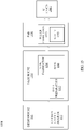
- FIG. 1 is a top view diagram of part of a semiconductor device, in accordance with some embodiments.
- FIG. 2 is a top view diagram of part of a semiconductor device, in accordance with some embodiments.
- FIG. 3 is a top view diagram of part of a semiconductor device, in accordance with some embodiments.
- FIG. 4 is a cross-section view diagram of part of a semiconductor device, in accordance with some embodiments.
- FIG. 5 is a top view diagram of part of the semiconductor device, in accordance with some embodiments.
- FIG. 6 is a cross-section view diagram of part of the semiconductor device in FIG. 5 , in accordance with some embodiments.
- FIG. 7 is a cross-section view diagram of part of a semiconductor device corresponding to that in FIG. 5 , in accordance with various embodiments.
- FIG. 8 is a cross-section view diagram of part of a semiconductor device corresponding to that in FIG. 5 , in accordance with various embodiments.
- FIG. 9 is a cross-section view diagram of part of a semiconductor device, in accordance with some embodiments.
- FIG. 10 is a cross-section view diagram of part of a semiconductor device, in accordance with some embodiments.
- FIG. 11 is a top view diagram of part of a semiconductor device, in accordance with some embodiments.
- FIG. 12 is a top view diagram of part of a semiconductor device, in accordance with some embodiments.
- FIG. 13 is a flow chart of a method of fabricating a semiconductor device, in accordance with some embodiments of the present disclosure.
- FIG. 14 is a block diagram of a system for designing the integrated circuit layout design, in accordance with some embodiments of the present disclosure.
- FIG. 15 is a block diagram of an integrated circuit manufacturing system, and an integrated circuit manufacturing flow associated therewith, in accordance with some embodiments.
- first and second features are formed in direct contact
- additional features may be formed between the first and second features, such that the first and second features may not be in direct contact
- present disclosure may repeat reference numerals and/or letters in the various examples. This repetition is for the purpose of simplicity and clarity and does not in itself dictate a relationship between the various embodiments and/or configurations discussed.
- spatially relative terms such as “beneath,” “below,” “lower,” “above,” “upper” and the like, may be used herein for ease of description to describe one element or feature's relationship to another element(s) or feature(s) as illustrated in the figures.
- the spatially relative terms are intended to encompass different orientations of the device in use or operation in addition to the orientation depicted in the figures.
- the apparatus may be otherwise oriented (rotated 90 degrees or at other orientations) and the spatially relative descriptors used herein may likewise be interpreted accordingly.
- the term “and/or” includes any and all combinations of one or more of the associated listed items.
- “around”, “about”, “approximately” or “substantially” shall generally refer to any approximate value of a given value or range, in which it is varied depending on various arts in which it pertains, and the scope of which should be accorded with the broadest interpretation understood by the person skilled in the art to which it pertains, so as to encompass all such modifications and similar structures. In some embodiments, it shall generally mean within 20 percent, preferably within 10 percent, and more preferably within 5 percent of a given value or range. Numerical quantities given herein are approximate, meaning that the term “around”, “about”, “approximately” or “substantially” can be inferred if not expressly stated, or meaning other approximate values.
- the present disclosure provides some implements to reduce insertion loss (IL) of an antenna switch without changing a circuit design of the antenna switch.
- an isolation feature is disposed adjacent a metal-oxide-semiconductor (MOS) device on a substrate.
- MOS metal-oxide-semiconductor
- less metal like element being disposed adjacent the device which receives and transmits signals further improves IL performance.
- non-implanted semiconductor structures are arranged adjacent to the MOS.
- semiconductor structures, such like dummy gates or dummy active areas are arranged adjacent to the MOS.
- a resist protect oxide (RPO) layer is formed above the semiconductor structures to prevent the structures under the RPO layers to be silicided.
- one terminal of the MOS corresponding to a substrate is set floated or coupled to a resistor.
- multiple MOSs are separated from each other with a predetermined spacing.
- the resistors coupled to the MOSs have a predetermined width and the resistors are separated from each other with another predetermined spacing.
- the substrate includes a non-doped region.
- the resistor(s) is disposed in metal layers above the non-doped region.
- shallow trench isolations and the MOS extend into the substrate, while the shallow trench isolations have a depth greater than a depth of the MOS.
- the substrate has a high resistivity.
- the MOS has an enlarged pitch between gate structures thereof, and conductive segments configured as drain/source terminal of the MOS have an enlarged width.
- Each of the above-mentioned embodiments can improve IL performance of the antenna switch based on a process technique without changing a circuit design of the antenna switch.
- the above-mentioned embodiments may be applied independently or in any combination. They improve IL performance without incurring any additional cost or any additional process complexity, or chip area penalty.
- the present disclosure is applicable to any semiconductor process technology for antenna switch, including but not limited to the fin field-effect transistor (FinFET) which is the next technology for 28 GHz 5G cellular networks.
- FinFET fin field-effect transistor
- FIG. 1 is a top view diagram of part of a semiconductor device 100 , in accordance with some embodiments.
- the semiconductor device 100 is formed to serve as an antenna switch.
- the semiconductor device 100 includes a substrate 110 , a metal-oxide-semiconductor device (MOS) 120 , and a feature 130 disposed adjacent to the MOS 120 .
- MOS metal-oxide-semiconductor device
- a conductivity of the feature 130 is smaller than a conductivity of the substrate 110 .
- the feature 130 extends into the substrate 110 with a first depth
- the metal-oxide-semiconductor device 120 extends into the substrate 110 with a second depth smaller than the first depth.
- the substrate 110 is pure silicon structure. In various embodiments, the substrate 110 includes other elementary semiconductors such as germanium.
- the substrate 110 includes a compound semiconductor such as silicon carbide, gallium arsenic, indium arsenide, and indium phosphide.
- Various implements of the substrate 110 are included in the contemplated scope of the present disclosure.
- the substrate 110 includes an alloy semiconductor such as silicon germanium, silicon germanium carbide, gallium arsenic phosphide, and gallium indium phosphide.
- FIG. 2 is a top view diagram of part of a semiconductor device 200 corresponding to the semiconductor device 100 of FIG. 1 , in accordance with some embodiments. With respect to the embodiments of FIG. 1 , like elements in FIG. 2 are designated with the same reference numbers for ease of understanding.
- the semiconductor device 200 includes multiple dummy structures 230 on the substrate 110 .
- the dummy structures 230 are configured with respect to, for example, the feature 130 of FIG. 1 .
- the dummy structures 230 are arranged apart from the MOS by a distance S 1 .
- the distance S 1 ranges from about 1 to about 100 micrometers.
- the dummy structures 230 include, for example, pure silicon structures.
- the dummy structures 230 are arranged in y direction in a form of an array.
- the dummy structures 230 are placed pair by pair, as shown in FIG. 2 . For example, two of the dummy structures 230 in one pair are much closer to each other, compared with another two of the dummy structures 230 in another pair.
- some dummy structures are disposed adjacent the MOS for further chemical mechanical polish (CMP) process on the MOS.
- CMP chemical mechanical polish
- those dummy structures are P-type-doped or/and N-type-doped and are arranged by automation placing utility.
- an antenna switch having doped dummy structures induces insertion loss (IL) of about 1.00 dB.
- the semiconductor device 200 reduces the IL to about 0.97 dB. Accordingly, the IL performance is improved by about 0.03 d dB, compared to the antenna switch in some approach.
- the dummy structures 230 are arranged adjacent the MOS 120 in x direction and separated from the MOS 120 with the distance S 1 .
- all of the dummy structures 230 are apart from each other by a uniform spacing in both x and y directions.
- FIG. 3 is a top view diagram of part of a semiconductor device 300 corresponding to the semiconductor device 100 of FIG. 1 , in accordance with some embodiments. With respect to the embodiments of FIGS. 1-2 , like elements in FIG. 3 are designated with the same reference numbers for ease of understanding.
- a resist protect oxide (RPO) layer including two portions 330 a - 330 b is formed over the dummy structures 230 .
- the dummy structures 230 and the resist protect oxide (RPO) layer portions 330 a - 330 b in the embodiments of FIG. 3 are configured with respect to, for example, the feature 130 of FIG. 1 .
- the portion 330 a is separated from the MOS 120 by a distance S 2 in y direction.
- the portion 330 b is separated from the MOS 120 by a distance S 3 in x direction.
- the distances S 2 -S 3 are the same.
- the distances S 2 -S 3 are different.
- the distances S 2 -S 3 range from about 1 to about 100 micrometers.
- areas and structures covered by the RPO layer portions 330 a - 330 b are not silicided in the process.
- the areas of the semiconductor device 300 are divided into areas that are to be silicided for electrical contacts and other areas that are not to be silicided. Accordingly, the dummy structures 230 under the RPO layer portion 330 a are not silicided.
- the RPO layer portions 330 a - 330 b are formed using silicon dioxide.
- some dummy structures are disposed adjacent the MOS are silicided and further have conductive features disposed thereon.
- an antenna switch having silicided dummy structures induces insertion loss (IL) of about 1.1 dB.
- the semiconductor device 300 reduces the IL to about 1.0 dB. Accordingly, the IL performance is improved by about 0.1 dB, compared to the antenna switch in some approach.
- FIG. 3 The configurations of FIG. 3 are given for illustrative purposes. Various implements are within the contemplated scope of the present disclosure. For example, in some embodiments, there are the dummy structures 230 arranged under the RPO layer portion 330 b.
- FIG. 4 is a cross-section view diagram of part of a semiconductor device 400 corresponding to the semiconductor device 100 of FIG. 1 , in accordance with some embodiments.
- the doped region 431 is disposed in the well 422 .
- the doped regions 432 - 435 are disposed in the well 423 .
- the doped region 436 is disposed in the well 424 .
- the doped region 437 is disposed in the well 425 .
- the doped regions 431 - 437 are separated by the shallow trench isolations STI.
- the doped regions 431 , 433 - 434 , and 436 are N-doped.
- the doped regions 432 , 435 , and 437 are P-doped.
- the gate 450 is disposed above the gate oxide layer 440 .
- the gate 450 is formed as a polysilicon (or poly) layer.
- the gate 450 further includes a gate dielectric layer (not shown) and a metal gate layer (not shown).
- the gate 450 includes one or more metal layers in place of the poly layer.
- the gate oxide layer 440 includes a dielectric material including, for example, silicon oxide (SiO 2 ) or silicon oxynitride (SiON), and is able to be formed by chemical oxidation, thermal oxidation, atomic layer deposition (ALD), chemical vapor deposition (CVD), and/or other suitable methods.
- the polysilicon layer is formed by suitable deposition processes including, for example, low-pressure chemical vapor deposition (LPCVD) and plasma-enhanced CVD (PECVD).
- the gate dielectric layer uses a high-k dielectric material including, for example, hafnium oxide (HfO 2 ), Al 2 O 3 , lanthanide oxides, TiO 2 , HfZrO, Ta 2 O 3 , HfSiO 4 , ZrO 2 , ZrSiO 2 , combinations thereof, or other suitable material, and the gate dielectric layer is formed by ALD and/or other suitable methods.
- the metal gate layer includes a p-type work function metal or an n-type work function metal, and is deposited by CVD, PVD, and/or other suitable process.
- exemplary p-type work function metals include TiN, TaN, Ru, Mo, Al, WN, ZrSi 2 , MoSi 2 , TaSi 2 , NiSi 2 , WN, other suitable p-type work function materials, or combinations thereof.
- Exemplary n-type work function metals include Ti, Ag, TaAl, TaAlC, TiAlN, TaC, TaCN, TaSiN, Mn, Zr, other suitable n-type work function materials, or combinations thereof.
- the one or more metal layers use aluminum (Al), tungsten (W), copper (Cu), cobalt (Co), and/or other suitable materials; and are formed by CVD, PVD, plating, and/or other suitable processes.
- Al aluminum
- tungsten (W) tungsten
- Cu copper
- Co cobalt
- the formations and/or materials associated with the gate 450 and the gate oxide layer 440 are given for illustrative purposes. Various formations and/or materials associated with the gate 450 and the gate oxide layer 440 are within the contemplated scope of the present disclosure.
- the doped regions 433 - 435 , the gate oxide layer 440 , and the gate 450 are included in a transistor TR 1 .
- the transistor TR 1 is configured with respect to, for example, the MOS 120 of FIG. 1 .
- the doped regions 433 - 435 are configured in the formations of a drain terminal T 1 , a source terminal T 3 , and a body terminal T 4 of the transistor TR 1 separately.
- the gate 450 corresponds to a gate terminal T 2 of the transistor TR 1 .
- the doped region 436 is configured in the formation of a terminal T 5 corresponding to the wells 421 and 424
- the doped region 437 is configured in the formation of a terminal T 6 corresponding to the substrate including a lower portion 410 of the substrate.
- the MOS device includes six terminals T 1 -T 6 in operation.
- the gate terminal T 2 , the terminals T 4 -T 6 , or the combination thereof is configured to be electrically coupled to a resistor(s) or to be floated.
- the gate terminal T 2 is coupled to a signal, i.e., a voltage VDD.
- the body terminal T 4 is coupled to the resistor R 1 and further to the ground.
- the terminal T 5 is coupled to the resistor R 2 and further to the ground.
- the terminal T 6 is floated.
- the terminal T 6 is coupled to a resistor configured with respect to, for example, the resistors R 1 -R 2 .
- the resistors R 1 -R 2 have a resistance of about 500 to about 1,000,000 ohms.
- the resistors R 1 -R 2 are resistors of sufficiently high value to effectively float the substrate.
- substrate noise coupling degrades the performance of the semiconductor device.
- a portion of a signal supposed to be transmitted from the drain to source flows from the wells 423 - 425 to the doped region 437
- another portion of the signal flows from the wells 423 , 421 , 424 - 425 to the doped region 437
- the other portion of the signal flows from the wells 423 , 421 , the lower portion 410 of the substrate, and the well 425 to the doped region 437 .
- an antenna switch having the terminal T 6 being floated or coupled to a resistor, reduces the IL about 1.0 dB, compared to the antenna switch in some approach.
- the terminals T-T 6 are both floated or coupled to the resistors, there is further a reduction of about 1.0 dB to the IL, with respect to only the terminal T 6 floated.
- the terminals T 4 -T 6 are all floated or coupled to the resistors, there is further a reduction of about 1.0 dB to the IL, with respect to the terminals T 5 -T 6 floated. Accordingly, the IL performance is much improved, compared to the antenna switch in some approach.
- the wells 421 - 422 and 424 are P-doped wells.
- the wells 423 and 425 are N-doped wells.
- the doped regions 431 , 433 - 434 , and 436 are P-doped.
- the doped regions 432 , 435 , and 437 are N-doped.
- FIG. 5 is a top view diagram of part of the semiconductor device 400 , in accordance with some embodiments. With respect to the embodiments of FIG. 4 , like elements in FIG. 5 are designated with the same reference numbers for ease of understanding.
- the semiconductor device 400 further includes wells 420 , a non-doped region 470 , resistors R, and transistors TR 2 .
- the wells 420 are configured with respect to, for example, the wells 421 - 425 of FIG. 4 .
- the non-doped region 470 corresponds to a region of the substrate including the lower portion 410 of the substrate.
- the resistors R are configured with respect to, for example, the resistors R 1 -R 2 of FIG. 4 .
- the transistors TR 2 are configured with respect to, for example, the transistor TR 1 having six terminals of FIG. 4 .
- one of the transistor TR 2 is implemented by coupling multiple transistors TR 1 in parallel.
- the transistors TR 2 are disposed within the wells 420 which extend in x direction.
- the transistors TR 2 are apart from each other by a distance S 4 in a layout view.
- the distance S 4 ranges from about 0.001 to about 5 micrometers.
- each of the transistors TR 2 has a MOS height of about 1.5 micrometers in y direction.
- the wells 420 are enclosed with the non-doped region 470 in the layout view.
- the transistors TR 2 are separated from the non-doped region 470 by a distance S 5 .
- the distance S 5 is about 1 micrometer, but the present disclosure is not limited thereto.
- the non-doped region 470 is referred to as non-doped Si (NTN) area in the substrate including the lower portion 410 of the substrate. The detail of the non-doped region 470 will be discussed with cross-section diagram in FIG. 6 .
- the resistors R are arranged above the non-doped region 470 .
- the non-doped region 470 corresponds to the non-doped region in the substrate including the lower portion 410 of the substrate.
- no P-well or N-well is arranged under the resistors R. Accordingly, in the embodiments above, the influence of the substrate noise coupling to the resistors R is reduced due to the distance, provided by the non-doped region, between the doped region of the substrate including the lower portion 410 of the substrate and the resistors R.
- the IL is correspondingly improved.
- the resistors R in a row are aligned with the transistor TR 2 in x direction. As shown in FIG. 5 , the resistors R are separated from each other in x direction with a distance S 6 , and each of the resistors R has a width W 1 .
- the distance S 6 ranges from about 0.001 to about 10 micrometers.
- the width W 1 ranges from about 0.001 to about 10 micrometers.
- resistors having a wider width suffer from the substrate noise coupling.
- the resistors have a reduced width and closer spacing between each other. Accordingly, the insertion loss due to the parasitic capacitance between the substrate and the resistors is reduced.
- the IL is correspondingly improved. For example, based on some experiment results, the induced IL drops about 0.2 dB when a width of resistors in an antenna switch changes from about 0.36 to about 0.06 micrometers.
- the resistors R are arranged on two opposite sides of the transistors TR 2 .
- FIG. 6 is a cross-section view diagram of part of the semiconductor device 400 along line AA′ in FIG. 5 , in accordance with some embodiments. With respect to the embodiments of FIGS. 4-5 , like elements in FIG. 6 are designated with the same reference numbers for ease of understanding.
- the semiconductor device 400 further includes multiple thick metal layers M 1 -M 4 , M(top- 1 ), and Mtop and an isolation 480 . In some embodiments, there are more metal layers between the metal layers M 4 and M(top- 1 ).
- the metal layers M 1 -M 4 , M(top- 1 ), and Mtop are configured for metal routing between devices included in the semiconductor device 400 .
- the isolation 480 is implemented by, for example, a shallow trench isolation or dummy active area, and is configured with respect to, for example, the feature 130 of FIG. 1 .
- the metal layers M 1 -M 4 , M(top- 1 ), and Mtop are arranged above the transistor TR 2 and the isolation 480 in z direction.
- the resistor R is arranged in a position of the metal layers. In some embodiments, the resistor R is arranged above at least one of the metal layers.
- the resistor R is arranged in a back-end-of-line (BEOL) portion, in which BEOL is the final portion of the IC fabrication process where the individual devices (transistors, capacitors, resistors, etc.) are interconnected with vias and conductive traces, e.g., metal layers M 1 -M 4 , M(top- 1 ) and Mtop.
- BEOL back-end-of-line
- the non-doped region 470 is arranged below the isolation 480 .
- the non-doped region 470 is non-doped silicon region of the substrate including the lower portion 410 of the substrate, including a semiconductor material, e.g. silicon, that has a higher impedance than that of an extrinsic semiconductor, e.g. a p-type semiconductor or a n-type semiconductor in the rest region of the substrate including the lower portion 410 of the substrate.
- an extrinsic semiconductor e.g. a p-type semiconductor or a n-type semiconductor in the rest region of the substrate including the lower portion 410 of the substrate.
- FIG. 6 The configurations of FIG. 6 are given for illustrative purposes. Various implements are within the contemplated scope of the present disclosure. For example, in some embodiments, another pair of the isolation 480 and the non-doped region 470 are arranged on both opposite sides of the transistor TR 2 in FIG. 6 .
- FIG. 7 is a cross-section view diagram of part of a semiconductor device 700 corresponding to that in FIG. 5 , in accordance with various embodiments. With respect to the embodiments of FIGS. 4-6 , like elements in FIG. 7 are designated with the same reference numbers for ease of understanding.
- the isolations 480 and the non-doped regions 470 are arranged on both opposite sides of the transistor TR 2 and adjacent the transistor TR 2 in FIG. 7 .
- the resistors R are further disposed above the non-doped regions 470 on both opposite sides of the transistor TR 2 .
- the resistors R are arranged in the position of the metal layer M 2 .
- FIG. 8 is a cross-section view diagram of part of a semiconductor device 800 corresponding to that in FIG. 5 , in accordance with various embodiments. With respect to the embodiments of FIGS. 4-7 , like elements in FIG. 8 are designated with the same reference numbers for ease of understanding.
- the resistors R in the semiconductor device 800 are arranged between the isolations 480 and the metal layer M 1 .
- the resistors R are disposed in middle-end-of-line (MEOL) portion, in which MEOL provides contacts (including the shared contacts) between the gates and source/drain regions of the devices.
- MEOL middle-end-of-line
- FIG. 9 is a cross-section view diagram of part of a semiconductor device 900 corresponding to the semiconductor device 100 of FIG. 1 , in accordance with some embodiments.
- the semiconductor device 900 includes a substrate 910 , a MOS 920 , and features 931 - 932 .
- the substrate 910 is configured with respect to, for example, the substrate 110 of FIG. 1 .
- the MOS 920 is configured with respect to, for example, the MOS 120 of FIG. 1 .
- the features 931 - 932 are configured with respect to, for example, the feature 130 of FIG. 1 .
- the MOS 920 and the features 931 - 932 extend into the substrate 910 in z direction, and the features 931 - 932 are disposed at the opposite sides of the MOS 920 .
- the features 931 - 932 include shallow trench isolations. As shown in FIG. 9 , the features 931 - 932 extend into the substrate 910 with a depth D 1 , and the MOS 920 extends into the substrate 910 with a depth D 2 . In some embodiments, the depth D 1 is greater than the depth D 2 . In various embodiments, the depths D 1 -D 2 ranges from about 0.5 to about 10 micrometers.
- FIG. 9 The configurations of FIG. 9 are given for illustrative purposes. Various implements are within the contemplated scope of the present disclosure. For example, in some embodiments, the depths of the features 931 - 932 are different due to the actual design.
- FIG. 10 is a cross-section view diagram of part of a semiconductor device 1000 corresponding to the semiconductor device 100 of FIG. 1 , in accordance with some embodiments. With respect to the embodiments of FIG. 9 , like elements in FIG. 10 are designated with the same reference numbers for ease of understanding.
- the depth D 1 is smaller than the depth D 2 .
- the substrate 910 is further has a high resistivity ranging from about 100 to about 1,000,000 ohm-cm.
- the substrate 910 includes a silicon wafer having a low doping concentration (e.g., a doping concentration that is less than 10 10 atoms/cm ⁇ 3 ).
- the IL due to the source-, drain-, and channel-to-substrate capacitances varies depending on the effective value of substrate resistance, with IL decreasing as the substrate resistance increases.
- the substrate resistance depends on substrate resistivity and layout. Accordingly, compared to some approaches including an antenna switch with a low-resistivity substrate, an antenna switch with the configurations of FIG. 10 reduces the IL about 0.5 dB.
- the substrate 910 further includes the regions 470 as shown in FIG. 8 to further improve the IL performance of the semiconductor device 1000 .
- FIG. 11 is a top view diagram of part of a semiconductor device 1100 corresponding to the semiconductor device 100 of FIG. 1 , in accordance with some embodiments. With respect to the embodiments of FIG. 4 , like elements in FIG. 11 are designated with the same reference numbers for ease of understanding.
- the semiconductor device 1100 includes transistors TR 3 .
- the configurations of the transistors TR 2 -TR 3 are different.
- the configurations of the transistors TR 2 -TR 3 are the same.
- one transistor TR 3 is a combination of more than 30 duplicated MOSs TR 3 coupled in parallel together.
- the transistors TR 3 have a MOS height, for example, around 1.5 micrometers.
- the distance S 4 ranges from about 0.001 to about 5 micrometers.
- the transistors M 3 have a MOS height, for example, around 1.5 micrometers.
- the distance S 4 ranges from about 0.001 to about 5 micrometers.
- the distance between MOSs is about 5 micrometers due to deep n-well rule.
- IL performance of the antenna switch is improved based on a process technique to shorten the distance between MOSs, without changing a circuit design of the antenna switch.
- a number of the MOS configured with respect to the transistors TR 3 are more than three.
- FIG. 12 is a top view diagram of part of a semiconductor device 1200 corresponding to the semiconductor device 100 of FIG. 1 , in accordance with some embodiments.
- the semiconductor device 1200 includes a substrate 1210 , a doped region 1220 , gates 1230 , and conductive segments (metal-to-device, MD) 1240 in a transistor TR 4 .
- the substrate 1210 is configured with respect to, for example, the substrate 110 of FIG. 1 .
- the transistor TR 4 is configured with respect to, for example, the MOS 120 of FIG. 1 .
- the doped region 1220 extends in x direction on the substrate 1210 .
- the gates 1230 extend in y direction and are separated from each other in x direction with a gate pitch P.
- the conductive segments 140 having a width W 2 , extend in y direction and are interposed between the gates 1230 .
- the gate pitch P ranges from about 100 to about 220 nanometers.
- the width W 2 is about 40 nanometers.
- an IL of an antenna switch reduces about 1.0 dB as the gate pitch thereof is enlarged from about 90 nanometers to 130 nanometers.
- having the enlarged conductive segment width contributes the improvement of the IL as well.
- an IL of an antenna switch reduces about 0.03 dB as the width of the conductive segments thereof is enlarged from about 24 nanometers to 40 nanometers.
- the IL of the antenna switch exhibits a significant improvement.
- the configurations of FIG. 12 are given for illustrative purposes. Various implements are within the contemplated scope of the present disclosure.
- the doped region 1220 is implemented with separated doped regions.
- FIG. 13 is a flow chart of a method 1300 of fabricating the semiconductor devices 100 , 200 , 300 , 400 , 700 , 800 , 900 , 1000 , 1100 , or 1200 , in accordance with some embodiments of the present disclosure. It is understood that additional operations can be provided before, during, and after the processes shown by FIG. 13 , and some of the operations described below can be replaced or eliminated, for additional embodiments of the method 1300 .
- the method 1300 includes operations 1301 - 1307 . The order of the operations shown in FIG. 13 may be changed according to different embodiments of the present disclosure.
- At least one MOS extending into a substrate is formed, as shown in the embodiments of, for example, FIGS. 6-10 .
- gates of the at least one MOS have an enlarged pitch and conductive segments of the at least one MOS have a predetermined width, as shown in the embodiments of, for example, FIG. 12 .
- At least one shallow trench isolation extending into the substrate is formed, as shown in the embodiments of, for example, FIGS. 6-10 .
- multiple semiconductor structures adjacent to the at least one MOS device on the substrate are formed, as shown in the embodiments of, for example, FIGS. 2-3 .
- a resist protect oxide layer over the semiconductor structures is formed, as shown in the embodiments of, for example, FIG. 3 .
- multiple MOSs of the at least one MOS device separated from each other by a predetermined spacing are formed, as shown in the embodiments of, for example, FIGS. 5 and 11 .
- At least one resistor coupled to at least one terminal of the at least one MOS, as shown in the embodiments of, for example, FIG. 4 .
- multiple resistors of the at least one resistor adjacent the MOSs are formed, as shown in the embodiments of, for example, FIG. 5 .
- the resistors are separated from each other by a predetermined spacing, as shown in the embodiments of, for example, FIGS. 5 and 11 .
- each of the resistors has a width, as shown in the embodiments of, for example, FIG. 5 .
- the resistors are arranged above non-doped region of the substrate, as shown in the embodiments of, for example, FIGS. 6-8 .
- FIG. 14 is a block diagram of electronic design automation (EDA) system 1400 for designing the integrated circuit layout design, in accordance with some embodiments of the present disclosure.
- EDA system 1400 is configured to implement one or more operations of the method 1300 disclosed in FIG. 13 , and further explained in conjunction with FIGS. 1-12 .
- EDA system 1400 includes an APR system.
- EDA system 1400 is a general purpose computing device including a hardware processor 1402 and a non-transitory, computer-readable storage medium 1404 .
- Storage medium 1404 is encoded with, i.e., stores, computer program code (instructions) 1406 , i.e., a set of executable instructions.
- Execution of instructions 1406 by hardware processor 1402 represents (at least in part) an EDA tool which implements a portion or all of, e.g., the method 11300 .
- the processor 1402 is electrically coupled to computer-readable storage medium 1404 via a bus 1408 .
- the processor 1402 is also electrically coupled to an I/O interface 1410 and a fabrication tool 1416 by bus 1408 .
- a network interface 1412 is also electrically connected to processor 1402 via bus 1408 .
- Network interface 1412 is connected to a network 1414 , so that processor 1402 and computer-readable storage medium 1404 are capable of connecting to external elements via network 1414 .
- the processor 1402 is configured to execute computer program code 1406 encoded in computer-readable storage medium 1404 in order to cause EDA system 1400 to be usable for performing a portion or all of the noted processes and/or methods.
- processor 1402 is a central processing unit (CPU), a multi-processor, a distributed processing system, an application specific integrated circuit (ASIC), and/or a suitable processing unit.
- computer-readable storage medium 1404 is an electronic, magnetic, optical, electromagnetic, infrared, and/or a semiconductor system (or apparatus or device).
- computer-readable storage medium 1404 includes a semiconductor or solid-state memory, a magnetic tape, a removable computer diskette, a random access memory (RAM), a read-only memory (ROM), a rigid magnetic disk, and/or an optical disk.
- computer-readable storage medium 1404 includes a compact disk-read only memory (CD-ROM), a compact disk-read/write (CD-R/W), and/or a digital video disc (DVD).
- storage medium 1404 stores computer program code 1406 configured to cause EDA system 1400 (where such execution represents (at least in part) the EDA tool) to be usable for performing a portion or all of the noted processes and/or methods.
- storage medium 1404 also stores information which facilitates performing a portion or all of the noted processes and/or methods.
- storage medium 1404 stores IC layout diagram 1420 of standard cells including such standard cells as disclosed herein, for example, a cell including in the semiconductor devices 100 , 200 , 300 , 400 , 700 , 800 , 900 , 1000 , 1100 , 1200 discussed above with respect to FIGS. 1-12 .
- EDA system 1400 includes I/O interface 1410 .
- I/O interface 1410 is coupled to external circuitry.
- I/O interface 1410 includes a keyboard, keypad, mouse, trackball, trackpad, touchscreen, and/or cursor direction keys for communicating information and commands to processor 1402 .
- EDA system 1400 also includes network interface 1412 coupled to processor 1402 .
- Network interface 1412 allows EDA system 1400 to communicate with network 1414 , to which one or more other computer systems are connected.
- Network interface 1412 includes wireless network interfaces such as BLUETOOTH, WIFI, WIMAX, GPRS, or WCDMA; or wired network interfaces such as ETHERNET, USB, or IEEE-1464.
- wireless network interfaces such as BLUETOOTH, WIFI, WIMAX, GPRS, or WCDMA
- wired network interfaces such as ETHERNET, USB, or IEEE-1464.
- a portion or all of noted processes and/or methods are implemented in two or more systems 1400 .
- EDA system 1400 also includes the fabrication tool 1416 coupled to processor 1402 .
- the fabrication tool 1416 is configured to fabricate integrated circuits, e.g., the semiconductor devices 100 , 200 , 300 , 400 , 700 , 800 , 900 , 1000 , 1100 , 1200 discussed above with respect to FIGS. 1-12 illustrated in FIGS. 1-12 , according to the design files processed by the processor 1402 .
- EDA system 1400 is configured to receive information through I/O interface 1410 .
- the information received through I/O interface 1410 includes one or more of instructions, data, design rules, libraries of standard cells, and/or other parameters for processing by processor 1402 .
- the information is transferred to processor 1402 via bus 1408 .
- EDA system 1400 is configured to receive information related to a UI through I/O interface 1410 .
- the information is stored in computer-readable medium 1404 as design specification 1422 .
- a portion or all of the noted processes and/or methods are implemented as a standalone software application for execution by a processor. In some embodiments, a portion or all of the noted processes and/or methods are implemented as a software application that is a part of an additional software application. In some embodiments, a portion or all of the noted processes and/or methods are implemented as a plug-in to a software application. In some embodiments, at least one of the noted processes and/or methods are implemented as a software application that is a portion of an EDA tool. In some embodiments, a portion or all of the noted processes and/or methods are implemented as a software application that is used by EDA system 1400 . In some embodiments, a layout diagram which includes standard cells is generated using a suitable layout generating tool.
- the processes are realized as functions of a program stored in a non-transitory computer readable recording medium.
- a non-transitory computer readable recording medium include, but are not limited to, external/removable and/or internal/built-in storage or memory unit, for example, one or more of an optical disk, such as a DVD, a magnetic disk, such as a hard disk, a semiconductor memory, such as a ROM, a RAM, a memory card, and the like.
- FIG. 15 is a block diagram of IC manufacturing system 1500 , and an IC manufacturing flow associated therewith, in accordance with some embodiments.
- IC manufacturing system 1500 based on a layout diagram, at least one of (A) one or more semiconductor masks or (B) at least one component in a layer of a semiconductor integrated circuit is fabricated using IC manufacturing system 1500 .
- IC manufacturing system 1500 includes entities, such as a design house 1520 , a mask house 1530 , and an IC manufacturer/fabricator (“fab”) 1550 , that interact with one another in the design, development, and manufacturing cycles and/or services related to manufacturing an IC device 1560 .
- the entities in IC manufacturing system 1500 are connected by a communications network.
- the communications network is a single network.
- the communications network is a variety of different networks, such as an intranet and the Internet.
- the communications network includes wired and/or wireless communication channels.
- Each entity interacts with one or more of the other entities and provides services to and/or receives services from one or more of the other entities.
- two or more of design house 1520 , mask house 1530 , and IC fab 1550 is owned by a single entity. In some embodiments, two or more of design house 1520 , mask house 1530 , and IC fab 1550 coexist in a common facility and use common resources.
- Design house (or design team) 1520 generates an IC design layout diagram 1522 .
- IC design layout diagram 1522 includes various geometrical patterns, for example, an IC layout design for an IC device 1560 , for example, the semiconductor devices 100 , 200 , 300 , 400 , 700 , 800 , 900 , 1000 , 1100 , 1200 discussed above with respect to FIGS. 1-12 illustrated in FIGS. 1-12 .
- the geometrical patterns correspond to patterns of metal, oxide, or semiconductor layers that make up the various components of IC device 1560 to be fabricated. The various layers combine to form various IC features.
- a portion of IC design layout diagram 1522 includes various IC features, such as an active region, gate electrode, source and drain, conductive segments or vias of an interlayer interconnection, to be formed in a semiconductor substrate (such as a silicon wafer) and various material layers disposed on the semiconductor substrate.
- Design house 1520 implements a proper design procedure to form IC design layout diagram 1522 .
- the design procedure includes one or more of logic design, physical design or place and route.
- IC design layout diagram 1522 is presented in one or more data files having information of the geometrical patterns.
- IC design layout diagram 1522 can be expressed in a GDSII file format or DFII file format.
- Mask house 1530 includes data preparation 1532 and mask fabrication 1544 .
- Mask house 1530 uses IC design layout diagram 1522 to manufacture one or more masks 1545 to be used for fabricating the various layers of IC device 1560 according to IC design layout diagram 1522 .
- Mask house 1530 performs mask data preparation 1532 , where IC design layout diagram 1522 is translated into a representative data file (“RDF”).
- Mask data preparation 1532 provides the RDF to mask fabrication 1544 .
- Mask fabrication 1544 includes a mask writer.
- a mask writer converts the RDF to an image on a substrate, such as a mask (reticle) 1545 or a semiconductor wafer 1553 .
- the IC design layout diagram 1522 is manipulated by mask data preparation 1532 to comply with particular characteristics of the mask writer and/or requirements of IC fab 1550 .
- data preparation 1532 and mask fabrication 1544 are illustrated as separate elements.
- data preparation 1532 and mask fabrication 1544 can be collectively referred to as mask data preparation.
- data preparation 1532 includes optical proximity correction (OPC) which uses lithography enhancement techniques to compensate for image errors, such as those that can arise from diffraction, interference, other process effects and the like. OPC adjusts IC design layout diagram 1522 .
- data preparation 1532 includes further resolution enhancement techniques (RET), such as off-axis illumination, sub-resolution assist features, phase-shifting masks, other suitable techniques, and the like or combinations thereof.
- RET resolution enhancement techniques
- ILT inverse lithography technology
- data preparation 1532 includes a mask rule checker (MRC) that checks the IC design layout diagram 1522 that has undergone processes in OPC with a set of mask creation rules which contain certain geometric and/or connectivity restrictions to ensure sufficient margins, to account for variability in semiconductor manufacturing processes, and the like.
- MRC modifies the IC design layout diagram 1522 to compensate for limitations during mask fabrication 1544 , which may undo part of the modifications performed by OPC in order to meet mask creation rules.
- data preparation 1532 includes lithography process checking (LPC) that simulates processing that will be implemented by IC fab 1550 to fabricate IC device 1560 .
- LPC simulates this processing based on IC design layout diagram 1522 to create a simulated manufactured device, such as IC device 1560 .
- the processing parameters in LPC simulation can include parameters associated with various processes of the IC manufacturing cycle, parameters associated with tools used for manufacturing the IC, and/or other aspects of the manufacturing process.
- LPC takes into account various factors, such as aerial image contrast, depth of focus (“DOF”), mask error enhancement factor (“MEEF”), other suitable factors, and the like or combinations thereof.
- DOF depth of focus
- MEEF mask error enhancement factor
- OPC and/or MRC are be repeated to further refine IC design layout diagram 1522 .
- data preparation 1532 includes additional features such as a logic operation (LOP) to modify the IC design layout diagram 1522 according to manufacturing rules. Additionally, the processes applied to IC design layout diagram 1522 during data preparation 1532 may be executed in a variety of different orders.
- LOP logic operation
- a mask 1545 or a group of masks 1545 are fabricated based on the modified IC design layout diagram 1522 .
- mask fabrication 1544 includes performing one or more lithographic exposures based on IC design layout diagram 1522 .
- an electron-beam (e-beam) or a mechanism of multiple e-beams is used to form a pattern on a mask (photomask or reticle) 1545 based on the modified IC design layout diagram 1522 .
- Mask 1545 can be formed in various technologies. In some embodiments, mask 1545 is formed using binary technology. In some embodiments, a mask pattern includes opaque regions and transparent regions.
- a radiation beam such as an ultraviolet (UV) beam, used to expose the image sensitive material layer (for example, photoresist) which has been coated on a wafer, is blocked by the opaque region and transmits through the transparent regions.
- a binary mask version of mask 1545 includes a transparent substrate (for example, fused quartz) and an opaque material (for example, chromium) coated in the opaque regions of the binary mask.
- mask 1545 is formed using a phase shift technology.
- PSM phase shift mask
- various features in the pattern formed on the phase shift mask are configured to have proper phase difference to enhance the resolution and imaging quality.
- the phase shift mask can be attenuated PSM or alternating PSM.
- the mask(s) generated by mask fabrication 1544 is used in a variety of processes. For example, such a mask(s) is used in an ion implantation process to form various doped regions in semiconductor wafer 1553 , in an etching process to form various etching regions in semiconductor wafer 1553 , and/or in other suitable processes.
- IC fab 1550 includes wafer fabrication 1552 .
- IC fab 1550 is an IC fabrication business that includes one or more manufacturing facilities for the fabrication of a variety of different IC products.
- IC Fab 1550 is a semiconductor foundry. For example, there may be a manufacturing facility for the front end fabrication of a plurality of IC products (front-end-of-line (FEOL) fabrication), while a second manufacturing facility may provide the back end fabrication for the interconnection and packaging of the IC products (back-end-of-line (BEOL) fabrication), and a third manufacturing facility may provide other services for the foundry business.
- FEOL front-end-of-line
- BEOL back-end-of-line
- IC fab 1550 uses mask(s) 1545 fabricated by mask house 1530 to fabricate IC device 1560 .
- IC fab 1550 at least indirectly uses IC design layout diagram 1522 to fabricate IC device 1560 .
- semiconductor wafer 1553 is fabricated by IC fab 1550 using mask(s) 1545 to form IC device 1560 .
- the IC fabrication includes performing one or more lithographic exposures based at least indirectly on IC design layout diagram 1522 .
- Semiconductor wafer 1553 includes a silicon substrate or other proper substrate having material layers formed thereon. Semiconductor wafer 1553 further includes one or more of various doped regions, dielectric features, multilevel interconnects, and the like (formed at subsequent manufacturing steps).
- antenna switch including in the semiconductor device provided in the present disclosure has an improved insertion loss and isolation through implementing the features presented in the embodiments mentioned above without changing a circuit design of the antenna switch.
- a semiconductor device including a substrate; a metal-oxide-semiconductor device disposed in the substrate; and a feature disposed adjacent to the metal-oxide-semiconductor device.
- the feature extends into the substrate with a first depth and the metal-oxide-semiconductor device extends into the substrate with a second depth smaller than the first depth.
- the feature includes multiple deep shallow trench isolations. The shallow trench isolations have the first depth ranging from about 0.5 to about 10 micrometers.
- the feature includes two deep shallow trench isolations disposed at the opposite sides of the metal-oxide-semiconductor device, and have the first depth greater than about 0.5 micrometers.
- the semiconductor device further includes a first well and a second well of a first type and a third well of a second type different from the first type on the substrate; a fourth well of the second type disposed above the first well, in which the second well is interposed between the third and fourth wells; a first doped region of the second type disposed in the second well and a second doped region of the first type disposed in the third well; a gate structure disposed above the fourth well; and third to fifth doped regions disposed in the fourth well, in which the third to fifth doped regions and the gate structure are included in a structure configured to operate as the metal-oxide-semiconductor device.
- the gate structure, the first doped region, the second doped region, the fifth doped region, or the combination thereof is configured to be electrically coupled to the feature or to be floated.
- the feature includes at least one resistor having a resistance of about 500 to about 1,000,000 ohms.
- the feature is arranged apart from the metal-oxide-semiconductor device by a distance.
- the feature includes multiple semiconductor structures; and a resist protect oxide (RPO) layer arranged over the semiconductor structures. The distance ranges from about 1 to about 100 micrometers.
- the semiconductor further includes multiple resistors arranged above the feature, in which the resistors are separated from each other in a direction, and each of the resistors has a width, along the direction, ranging from about 0.001 to about 10 micrometers. In some embodiments, the resistors are apart from each other by a distance ranging from about 0.001 to about 10 micrometers.
- the substrate includes an extrinsic substrate and an intrinsic substrate arranged between the feature and the extrinsic substrate.
- the intrinsic substrate includes a material that has a higher impedance than that of the extrinsic substrate.
- the semiconductor device further includes a resistor arranged above the feature and the intrinsic substrate.
- the semiconductor device further includes multiple metal layers arranged above the feature.
- the resistor is arranged in one of the metal layers.
- the metal-oxide-semiconductor device includes multiple metal-oxide-semiconductor devices separated from each other in a distance in a layout view. The distance ranges from about 0.001 to about 5 micrometers.
- the substrate has a resistivity ranging from about 100 to about 1,000,000 ohm-cm.
- a semiconductor device that includes a substrate; first well to third well that are disposed in the substrate; first and second doped regions disposed in a fourth well above the first well, in which second well is interposed between the third and fourth well; and a third doped region disposed in the third well.
- the third doped region is configured to be floated.
- the semiconductor device includes multiple resistors; and a fourth doped region disposed in the first well and a fifth doped region disposed in the second well.
- the fourth doped region, the fifth doped region, or the combination thereof is configured to be coupled to at least one of the resistors.
- the resistors are separated from each other with a predetermined spacing.
- the semiconductor further includes multiple metal layers above the substrate; and at least one resistor disposed above at least one of the metal layers.
- the substrate includes an extrinsic substrate; and an intrinsic substrate arranged between the extrinsic substrate and the metal layers, in which the intrinsic substrate includes a material that has a higher impedance than that of the extrinsic substrate.
- the at least one resistor is further disposed above the intrinsic substrate.
- the first and second doped regions are included in each one of multiple metal-oxide-semiconductor devices. The plurality of metal-oxide-semiconductor devices are separated from each other by a distance which ranges from about 0.001 to 5 micrometers.
- a semiconductor device includes a substrate including a non-doped region; a metal-oxide-semiconductor device extending into the substrate, in which the metal-oxide-semiconductor device are adjacent to the non-doped region; and at least one resistor disposed right above the non-doped region and arranged in a row aligned with the metal-oxide-semiconductor device in a direction.
- the at least one resistor includes multiple resistors, in which each of the resistors has a width ranging from about 0.001 to about 10 micrometers and a minimum resistance of about 500 ohms.
- the metal-oxide-semiconductor device includes multiple gate structures having a pitch ranging from about 100 to about 220 nanometers; and multiple conductive segments having a width of about 40 nanometers.
Landscapes
- Semiconductor Integrated Circuits (AREA)
- Metal-Oxide And Bipolar Metal-Oxide Semiconductor Integrated Circuits (AREA)
- Engineering & Computer Science (AREA)
- General Engineering & Computer Science (AREA)
Abstract
Description
-
- For illustration, the semiconductor device 400 includes a substrate including a
lower portion 410 of the substrate, wells 421-425, shallow trench isolations STI, doped regions 431-437, agate oxide layer 440, agate structure 450, and resistors R1-R2. In some embodiments, the substrate including alower portion 410 of the substrate is configured with respect to, for example, the substrate no ofFIG. 1 . - As shown in
FIG. 4 , the wells 421-425 are disposed within the substrate including alower portion 410 of the substrate. The well 423 is arranged above thewell 421. The well 424 is further interposed between thewells wells wells
- For illustration, the semiconductor device 400 includes a substrate including a
Claims (20)
Priority Applications (10)
| Application Number | Priority Date | Filing Date | Title |
|---|---|---|---|
| US16/874,536 US11380680B2 (en) | 2019-07-12 | 2020-05-14 | Semiconductor device for a low-loss antenna switch |
| TW109116770A TWI747292B (en) | 2019-07-12 | 2020-05-20 | Semiconductor device |
| DE102020113596.3A DE102020113596A1 (en) | 2019-07-12 | 2020-05-20 | SEMI-CONDUCTOR DEVICE FOR A LOW-LOSS ANTENNA SWITCH |
| CN202010662287.XA CN112216693B (en) | 2019-07-12 | 2020-07-10 | Semiconductor device with a semiconductor layer having a plurality of semiconductor layers |
| KR1020200086242A KR102524237B1 (en) | 2019-07-12 | 2020-07-13 | Semiconductor device for a low-loss antenna switch |
| US17/853,596 US12021078B2 (en) | 2019-07-12 | 2022-06-29 | Semiconductor device for a low-loss antenna switch |
| US17/853,616 US12080706B2 (en) | 2019-07-12 | 2022-06-29 | Semiconductor device for a low-loss antenna switch |
| US18/669,378 US12501691B2 (en) | 2019-07-12 | 2024-05-20 | Semiconductor device for a low-loss antenna switch |
| US18/773,203 US12501692B2 (en) | 2019-07-12 | 2024-07-15 | Semiconductor device for a low-loss antenna switch |
| US19/391,949 US20260075928A1 (en) | 2019-07-12 | 2025-11-17 | Semiconductor device for a low-loss antenna switch |
Applications Claiming Priority (2)
| Application Number | Priority Date | Filing Date | Title |
|---|---|---|---|
| US201962873650P | 2019-07-12 | 2019-07-12 | |
| US16/874,536 US11380680B2 (en) | 2019-07-12 | 2020-05-14 | Semiconductor device for a low-loss antenna switch |
Related Child Applications (2)
| Application Number | Title | Priority Date | Filing Date |
|---|---|---|---|
| US17/853,616 Division US12080706B2 (en) | 2019-07-12 | 2022-06-29 | Semiconductor device for a low-loss antenna switch |
| US17/853,596 Continuation US12021078B2 (en) | 2019-07-12 | 2022-06-29 | Semiconductor device for a low-loss antenna switch |
Publications (2)
| Publication Number | Publication Date |
|---|---|
| US20210013195A1 US20210013195A1 (en) | 2021-01-14 |
| US11380680B2 true US11380680B2 (en) | 2022-07-05 |
Family
ID=74103246
Family Applications (1)
| Application Number | Title | Priority Date | Filing Date |
|---|---|---|---|
| US16/874,536 Active US11380680B2 (en) | 2019-07-12 | 2020-05-14 | Semiconductor device for a low-loss antenna switch |
Country Status (2)
| Country | Link |
|---|---|
| US (1) | US11380680B2 (en) |
| KR (1) | KR102524237B1 (en) |
Citations (14)
| Publication number | Priority date | Publication date | Assignee | Title |
|---|---|---|---|---|
| US6207998B1 (en) * | 1998-07-23 | 2001-03-27 | Mitsubishi Denki Kabushiki Kaisha | Semiconductor device with well of different conductivity types |
| US6213869B1 (en) * | 1999-05-10 | 2001-04-10 | Advanced Micro Devices, Inc. | MOSFET-type device with higher driver current and lower steady state power dissipation |
| US20020125537A1 (en) | 2000-05-30 | 2002-09-12 | Ting-Wah Wong | Integrated radio frequency circuits |
| US20040164354A1 (en) | 2001-06-14 | 2004-08-26 | Sarnoff Corporation | Minimum-dimension, fully- silicided MOS driver and ESD protection design for optimized inter-finger coupling |
| US20050221787A1 (en) * | 2000-05-30 | 2005-10-06 | Ting-Wah Wong | Integrated radio frequency circuits |
| US7348830B2 (en) * | 2003-09-26 | 2008-03-25 | Atmel Grenoble | Integrated circuit with automatic start-up function |
| TW200828446A (en) | 2006-12-29 | 2008-07-01 | Taiwan Semiconductor Mfg | Semiconductor device, metal oxide semiconductor device and method for forming metal oxide semiconductor device |
| US20100068873A1 (en) | 2008-09-16 | 2010-03-18 | Jing-Cheng Lin | Depletion-Free MOS using Atomic-Layer Doping |
| US20100207679A1 (en) * | 2009-02-19 | 2010-08-19 | Nec Electronics Corporation | Conduction switching circuit, conduction switching circuit block, and operating method of conduction switching circuit |
| CN102214693A (en) | 2010-04-09 | 2011-10-12 | 台湾积体电路制造股份有限公司 | Semiconductor device |
| US20130271223A1 (en) * | 2012-04-13 | 2013-10-17 | Taiwan Semiconductor Manufacturing Co., Ltd. | Amplifier with floating well |
| TW201630126A (en) | 2015-02-13 | 2016-08-16 | 台灣積體電路製造股份有限公司 | Semiconductor device structure and method for forming the same |
| US20160300830A1 (en) | 2015-04-07 | 2016-10-13 | Analog Devices, Inc. | High speed interface protection apparatus |
| US20190304937A1 (en) | 2018-03-29 | 2019-10-03 | Taiwan Semiconductor Manufacturing Co., Ltd. | Devices and methods for enhancing insertion loss performance of an antenna switch |
Family Cites Families (2)
| Publication number | Priority date | Publication date | Assignee | Title |
|---|---|---|---|---|
| KR20090031354A (en) * | 2008-12-09 | 2009-03-25 | 에이저 시스템즈 인크 | Bipolar Junction Transistors with Reduced Collector-Board Capacitance |
| JP6222825B2 (en) * | 2012-11-07 | 2017-11-01 | エヌエックスピー ユーエスエイ インコーポレイテッドNXP USA,Inc. | SEMICONDUCTOR DEVICE AND DRIVER CIRCUIT HAVING ACTIVE ELEMENT AND ISOLATED STRUCTURE INTERCONNECTED THROUGH DIODE CIRCUIT AND METHOD FOR MANUFACTURING THE SAME |
-
2020
- 2020-05-14 US US16/874,536 patent/US11380680B2/en active Active
- 2020-07-13 KR KR1020200086242A patent/KR102524237B1/en active Active
Patent Citations (20)
| Publication number | Priority date | Publication date | Assignee | Title |
|---|---|---|---|---|
| US6207998B1 (en) * | 1998-07-23 | 2001-03-27 | Mitsubishi Denki Kabushiki Kaisha | Semiconductor device with well of different conductivity types |
| US6213869B1 (en) * | 1999-05-10 | 2001-04-10 | Advanced Micro Devices, Inc. | MOSFET-type device with higher driver current and lower steady state power dissipation |
| US20020125537A1 (en) | 2000-05-30 | 2002-09-12 | Ting-Wah Wong | Integrated radio frequency circuits |
| US20050221787A1 (en) * | 2000-05-30 | 2005-10-06 | Ting-Wah Wong | Integrated radio frequency circuits |
| US20040164354A1 (en) | 2001-06-14 | 2004-08-26 | Sarnoff Corporation | Minimum-dimension, fully- silicided MOS driver and ESD protection design for optimized inter-finger coupling |
| JP2003152098A (en) | 2001-09-06 | 2003-05-23 | Programmable Silicon Solutions | Radio frequency integrated circuits |
| JP2006518941A (en) | 2003-02-20 | 2006-08-17 | サーノフ コーポレーション | Design of minimum-size full-silicide MOS driver and ESD protection for optimal inter-finger coupling |
| US7348830B2 (en) * | 2003-09-26 | 2008-03-25 | Atmel Grenoble | Integrated circuit with automatic start-up function |
| TW200828446A (en) | 2006-12-29 | 2008-07-01 | Taiwan Semiconductor Mfg | Semiconductor device, metal oxide semiconductor device and method for forming metal oxide semiconductor device |
| US20080157119A1 (en) | 2006-12-29 | 2008-07-03 | Pang-Yen Tsai | Stack SiGe for short channel improvement |
| US20100068873A1 (en) | 2008-09-16 | 2010-03-18 | Jing-Cheng Lin | Depletion-Free MOS using Atomic-Layer Doping |
| TW201013846A (en) | 2008-09-16 | 2010-04-01 | Taiwan Semiconductor Mfg | Depletion-free MOS using atomic-layer doping |
| US20100207679A1 (en) * | 2009-02-19 | 2010-08-19 | Nec Electronics Corporation | Conduction switching circuit, conduction switching circuit block, and operating method of conduction switching circuit |
| CN102214693A (en) | 2010-04-09 | 2011-10-12 | 台湾积体电路制造股份有限公司 | Semiconductor device |
| US20130271223A1 (en) * | 2012-04-13 | 2013-10-17 | Taiwan Semiconductor Manufacturing Co., Ltd. | Amplifier with floating well |
| TW201630126A (en) | 2015-02-13 | 2016-08-16 | 台灣積體電路製造股份有限公司 | Semiconductor device structure and method for forming the same |
| US20160240536A1 (en) | 2015-02-13 | 2016-08-18 | Taiwan Semiconductor Manufacturing Co., Ltd | Structure and formation method of finfet device |
| US20160300830A1 (en) | 2015-04-07 | 2016-10-13 | Analog Devices, Inc. | High speed interface protection apparatus |
| US9673187B2 (en) * | 2015-04-07 | 2017-06-06 | Analog Devices, Inc. | High speed interface protection apparatus |
| US20190304937A1 (en) | 2018-03-29 | 2019-10-03 | Taiwan Semiconductor Manufacturing Co., Ltd. | Devices and methods for enhancing insertion loss performance of an antenna switch |
Also Published As
| Publication number | Publication date |
|---|---|
| US20210013195A1 (en) | 2021-01-14 |
| KR102524237B1 (en) | 2023-04-20 |
| KR20210008321A (en) | 2021-01-21 |
Similar Documents
| Publication | Publication Date | Title |
|---|---|---|
| US11374003B2 (en) | Integrated circuit | |
| US11830869B2 (en) | Integrated circuit | |
| US11842963B2 (en) | Semiconductor device and method | |
| US12237332B2 (en) | Integrated circuit | |
| US20250259930A1 (en) | Integrated circuit device and method | |
| US20250169189A1 (en) | Integrated circuit and method of forming the same | |
| US20260075928A1 (en) | Semiconductor device for a low-loss antenna switch | |
| US20250357346A1 (en) | Method of manufacturing integrated circuit structure including first metal structure | |
| US20240371753A1 (en) | Source/drain isolation structure and layout method | |
| US20250185362A1 (en) | Integrated circuit and method of forming the same | |
| US20240266346A1 (en) | Power Distribution Network | |
| US12131998B2 (en) | Integrated circuit, system and method of forming same | |
| US11380680B2 (en) | Semiconductor device for a low-loss antenna switch | |
| US20250372514A1 (en) | Feed-through via device, layout, and method | |
| US20260068324A1 (en) | Integrated circuit and method of forming the same | |
| US20250273573A1 (en) | Integrated circuit and method of forming the same | |
| US11695413B2 (en) | Integrated circuit and method of manufacturing same |
Legal Events
| Date | Code | Title | Description |
|---|---|---|---|
| FEPP | Fee payment procedure |
Free format text: ENTITY STATUS SET TO UNDISCOUNTED (ORIGINAL EVENT CODE: BIG.); ENTITY STATUS OF PATENT OWNER: LARGE ENTITY |
|
| AS | Assignment |
Owner name: TAIWAN SEMICONDUCTOR MANUFACTURING CO., LTD., TAIWAN Free format text: ASSIGNMENT OF ASSIGNORS INTEREST;ASSIGNORS:JIN, JUN-DE;YEH, TZU-JIN;REEL/FRAME:052780/0363 Effective date: 20200515 |
|
| STPP | Information on status: patent application and granting procedure in general |
Free format text: APPLICATION DISPATCHED FROM PREEXAM, NOT YET DOCKETED |
|
| STPP | Information on status: patent application and granting procedure in general |
Free format text: DOCKETED NEW CASE - READY FOR EXAMINATION |
|
| STPP | Information on status: patent application and granting procedure in general |
Free format text: NON FINAL ACTION MAILED |
|
| STPP | Information on status: patent application and granting procedure in general |
Free format text: RESPONSE TO NON-FINAL OFFICE ACTION ENTERED AND FORWARDED TO EXAMINER |
|
| STPP | Information on status: patent application and granting procedure in general |
Free format text: NON FINAL ACTION MAILED |
|
| STPP | Information on status: patent application and granting procedure in general |
Free format text: NOTICE OF ALLOWANCE MAILED -- APPLICATION RECEIVED IN OFFICE OF PUBLICATIONS |
|
| STPP | Information on status: patent application and granting procedure in general |
Free format text: PUBLICATIONS -- ISSUE FEE PAYMENT VERIFIED |
|
| STCF | Information on status: patent grant |
Free format text: PATENTED CASE |
|
| MAFP | Maintenance fee payment |
Free format text: PAYMENT OF MAINTENANCE FEE, 4TH YEAR, LARGE ENTITY (ORIGINAL EVENT CODE: M1551); ENTITY STATUS OF PATENT OWNER: LARGE ENTITY Year of fee payment: 4 |