US11380353B1 - Magnetic head including spin torque oscillator, first and second gap films, and first and second guard films, and manufacturing method for the same - Google Patents
Magnetic head including spin torque oscillator, first and second gap films, and first and second guard films, and manufacturing method for the same Download PDFInfo
- Publication number
- US11380353B1 US11380353B1 US17/313,417 US202117313417A US11380353B1 US 11380353 B1 US11380353 B1 US 11380353B1 US 202117313417 A US202117313417 A US 202117313417A US 11380353 B1 US11380353 B1 US 11380353B1
- Authority
- US
- United States
- Prior art keywords
- shield
- main pole
- film
- films
- guard
- Prior art date
- Legal status (The legal status is an assumption and is not a legal conclusion. Google has not performed a legal analysis and makes no representation as to the accuracy of the status listed.)
- Active
Links
Images


Classifications
-
- G—PHYSICS
- G11—INFORMATION STORAGE
- G11B—INFORMATION STORAGE BASED ON RELATIVE MOVEMENT BETWEEN RECORD CARRIER AND TRANSDUCER
- G11B5/00—Recording by magnetisation or demagnetisation of a record carrier; Reproducing by magnetic means; Record carriers therefor
- G11B5/127—Structure or manufacture of heads, e.g. inductive
- G11B5/187—Structure or manufacture of the surface of the head in physical contact with, or immediately adjacent to the recording medium; Pole pieces; Gap features
- G11B5/23—Gap features
- G11B5/235—Selection of material for gap filler
-
- G—PHYSICS
- G11—INFORMATION STORAGE
- G11B—INFORMATION STORAGE BASED ON RELATIVE MOVEMENT BETWEEN RECORD CARRIER AND TRANSDUCER
- G11B5/00—Recording by magnetisation or demagnetisation of a record carrier; Reproducing by magnetic means; Record carriers therefor
- G11B5/127—Structure or manufacture of heads, e.g. inductive
- G11B5/1278—Structure or manufacture of heads, e.g. inductive specially adapted for magnetisations perpendicular to the surface of the record carrier
-
- G—PHYSICS
- G11—INFORMATION STORAGE
- G11B—INFORMATION STORAGE BASED ON RELATIVE MOVEMENT BETWEEN RECORD CARRIER AND TRANSDUCER
- G11B5/00—Recording by magnetisation or demagnetisation of a record carrier; Reproducing by magnetic means; Record carriers therefor
- G11B5/127—Structure or manufacture of heads, e.g. inductive
- G11B5/31—Structure or manufacture of heads, e.g. inductive using thin films
- G11B5/3109—Details
- G11B5/313—Disposition of layers
- G11B5/3133—Disposition of layers including layers not usually being a part of the electromagnetic transducer structure and providing additional features, e.g. for improving heat radiation, reduction of power dissipation, adaptations for measurement or indication of gap depth or other properties of the structure
- G11B5/314—Disposition of layers including layers not usually being a part of the electromagnetic transducer structure and providing additional features, e.g. for improving heat radiation, reduction of power dissipation, adaptations for measurement or indication of gap depth or other properties of the structure where the layers are extra layers normally not provided in the transducing structure, e.g. optical layers
-
- G—PHYSICS
- G11—INFORMATION STORAGE
- G11B—INFORMATION STORAGE BASED ON RELATIVE MOVEMENT BETWEEN RECORD CARRIER AND TRANSDUCER
- G11B5/00—Recording by magnetisation or demagnetisation of a record carrier; Reproducing by magnetic means; Record carriers therefor
- G11B5/127—Structure or manufacture of heads, e.g. inductive
- G11B5/31—Structure or manufacture of heads, e.g. inductive using thin films
- G11B5/3109—Details
- G11B5/313—Disposition of layers
- G11B5/3143—Disposition of layers including additional layers for improving the electromagnetic transducing properties of the basic structure, e.g. for flux coupling, guiding or shielding
- G11B5/3146—Disposition of layers including additional layers for improving the electromagnetic transducing properties of the basic structure, e.g. for flux coupling, guiding or shielding magnetic layers
-
- G—PHYSICS
- G11—INFORMATION STORAGE
- G11B—INFORMATION STORAGE BASED ON RELATIVE MOVEMENT BETWEEN RECORD CARRIER AND TRANSDUCER
- G11B5/00—Recording by magnetisation or demagnetisation of a record carrier; Reproducing by magnetic means; Record carriers therefor
- G11B2005/0002—Special dispositions or recording techniques
- G11B2005/0005—Arrangements, methods or circuits
- G11B2005/0024—Microwave assisted recording
-
- G—PHYSICS
- G11—INFORMATION STORAGE
- G11B—INFORMATION STORAGE BASED ON RELATIVE MOVEMENT BETWEEN RECORD CARRIER AND TRANSDUCER
- G11B5/00—Recording by magnetisation or demagnetisation of a record carrier; Reproducing by magnetic means; Record carriers therefor
- G11B5/127—Structure or manufacture of heads, e.g. inductive
- G11B5/31—Structure or manufacture of heads, e.g. inductive using thin films
- G11B5/3109—Details
- G11B5/313—Disposition of layers
- G11B5/3143—Disposition of layers including additional layers for improving the electromagnetic transducing properties of the basic structure, e.g. for flux coupling, guiding or shielding
- G11B5/3146—Disposition of layers including additional layers for improving the electromagnetic transducing properties of the basic structure, e.g. for flux coupling, guiding or shielding magnetic layers
- G11B5/315—Shield layers on both sides of the main pole, e.g. in perpendicular magnetic heads
-
- G—PHYSICS
- G11—INFORMATION STORAGE
- G11B—INFORMATION STORAGE BASED ON RELATIVE MOVEMENT BETWEEN RECORD CARRIER AND TRANSDUCER
- G11B5/00—Recording by magnetisation or demagnetisation of a record carrier; Reproducing by magnetic means; Record carriers therefor
- G11B5/127—Structure or manufacture of heads, e.g. inductive
- G11B5/33—Structure or manufacture of flux-sensitive heads, i.e. for reproduction only; Combination of such heads with means for recording or erasing only
- G11B5/39—Structure or manufacture of flux-sensitive heads, i.e. for reproduction only; Combination of such heads with means for recording or erasing only using magneto-resistive devices or effects
- G11B5/3903—Structure or manufacture of flux-sensitive heads, i.e. for reproduction only; Combination of such heads with means for recording or erasing only using magneto-resistive devices or effects using magnetic thin film layers or their effects, the films being part of integrated structures
- G11B5/3906—Details related to the use of magnetic thin film layers or to their effects
- G11B5/3912—Arrangements in which the active read-out elements are transducing in association with active magnetic shields, e.g. magnetically coupled shields
Definitions
- the present invention relates to a magnetic head including a spin torque oscillator, and a manufacturing method for the same.
- the recording systems of magnetic read/write apparatuses include a longitudinal magnetic recording system in which the magnetization of signals is directed along the plane of a recording medium (the longitudinal direction), and a perpendicular magnetic recording system in which the magnetization of signals is directed perpendicular to the plane of a recording medium. It is known that the perpendicular magnetic recording system is less likely to be affected by thermal fluctuation of the recording medium and capable of providing higher linear recording density, compared with the longitudinal magnetic recording system.
- Magnetic heads for perpendicular magnetic recording typically have, like those for longitudinal magnetic recording, a structure in which a read head unit having a magnetoresistive element (hereinafter, also referred to as MR element) for reading and a write head unit having an induction-type electromagnetic transducer for writing are stacked on a substrate.
- the write head unit includes a coil and a magnetic path forming section.
- the coil generates a magnetic field corresponding to data to be written on the recording medium.
- the magnetic path forming section is made of a magnetic material and forms a magnetic path for passing a magnetic flux corresponding to the magnetic field generated by the coil.
- the magnetic path forming section includes, for example, a main pole, a trailing shield, a first side shield, a second side shield, and a return path section.
- the main pole has a first end face located in a medium facing surface configured to face a recording medium.
- the trailing shield has a second end face located in the medium facing surface at a position forward relative to the first end face in a direction of travel of the recording medium.
- the return path section magnetically connects part of the main pole away from the medium facing surface to the trailing shield.
- the main pole generates, from the first end face, a write magnetic field for writing data on the recording medium.
- the first and second side shields are opposed to each other in a track width direction with the main pole therebetween.
- the first side shield has a third end face located in the medium facing surface.
- the second side shield has a fourth end face located in the medium facing surface.
- the third and fourth end faces are opposed to each other in the track width direction with the first end face therebetween.
- the third and fourth end faces are located backward relative to the second end face in the direction of travel of the recording medium.
- U.S. Pat. Nos. 8,320,079 B2, 8,917,481 B2, 10,032,470 B1, and 10,109,302 B1 each disclose a technology of using a spin torque oscillator that generates a microwave magnetic field. According to the technology, a microwave magnetic field is generated by the spin torque oscillator, and the microwave magnetic field and the write magnetic field are simultaneously applied to a portion of the recording medium on which data is to be written.
- the recording density it is effective to increase the coercivity of the recording medium by making magnetic fine particles of the recording medium smaller and, at the same time, enhancing the anisotropic energy of the magnetic fine particles.
- the aforementioned technology enables data writing with the coercivity of the recording medium lowered by microwaves, thus enabling use of a recording medium having high coercivity.
- U.S. Patent Application Publication No. 2018/0075868 A1 discloses a technology of using a spin torque oscillator that adjusts magnetic permeability.
- the spin torque oscillator blocks magnetic flux leaking from the main pole to the trailing shield.
- the technology makes it possible to make a gap between the main pole and the shield smaller. This in turn makes it possible to steepen the gradient of change in the strength of the write magnetic field to thereby increase the recording density.
- the spin torque oscillator is disposed between the main pole and the trailing shield and electrically connected to the main pole and the trailing shield.
- a current for operating the spin torque oscillator is supplied via the main pole and the trailing shield.
- a surface of the spin torque oscillator to be opposed to the main pole will be referred to as a bottom surface of the spin torque oscillator
- a surface of the spin torque oscillator to be opposed to the trailing shield will be referred to as a top surface of the spin torque oscillator.
- a surface of the main pole to be opposed to the trailing shield will be referred to as a top surface of the main pole.
- a surface of the trailing shield to be opposed to the main pole will be referred to as a bottom surface of the trailing shield.
- a spin torque oscillator is formed as follows.
- a layered film to later become the spin torque oscillator is initially formed on the top surface of the main pole, and then the layered film is patterned by etching so that a plurality of surfaces of the spin torque oscillator other than the top and bottom surfaces are formed in the layered film.
- a width in the track width direction will be simply referred to as a width.
- the top surface of the spin torque oscillator is usually formed with a smaller width than that of the bottom surface of the spin torque oscillator. This causes problems including heat generation of the spin torque oscillator and insufficient exertion of the foregoing function of the spin torque oscillator.
- An object of the present invention is to provide a magnetic head including a spin torque oscillator, where distances between a trailing shield and side shields near the spin torque oscillator can be controlled, and a manufacturing method for the same.
- a magnetic head includes: a medium facing surface configured to face a recording medium; a main pole configured to generate a write magnetic field for writing data on the recording medium; a trailing shield formed of a magnetic material and located forward relative to the main pole in a direction of travel of the recording medium; a spin torque oscillator located between the main pole and the trailing shield and electrically connected to the main pole and the trailing shield; first and second side shields formed of a magnetic material and opposed to each other in a track width direction with the main pole between the first and second side shields; first and second gap films formed of a nonmagnetic material and opposed to each other in the track width direction with the spin torque oscillator between the first and second gap films.
- the first gap film and the first guard film are interposed between the trailing shield and the first side shield.
- the second gap film and the second guard film are interposed between the trailing shield and the second side shield.
- the first and second gap films may be in contact with the spin torque oscillator.
- the first and second guard films may be not in contact with the spin torque oscillator.
- the first guard film may be interposed between the first gap film and the first side shield.
- the second guard film may be interposed between the second gap film and the second side shield.
- a distance between the trailing shield and the first side shield in the medium facing surface and a distance between the trailing shield and the second side shield in the medium facing surface may each be the same as a distance between the main pole and the trailing shield in the medium facing surface.
- the distance between the trailing shield and the first side shield in the medium facing surface and the distance between the trailing shield and the second side shield in the medium facing surface may each be greater or smaller than the distance between the main pole and the trailing shield in the medium facing surface.
- the first and second guard films may be formed of a nonmagnetic insulating material or a nonmagnetic metal material.
- a magnetic head manufactured by a manufacturing method for a magnetic head according to the present invention includes: a medium facing surface configured to face a recording medium; a main pole configured to generate a write magnetic field for writing data on the recording medium; a trailing shield formed of a magnetic material and located forward relative to the main pole in a direction of travel of the recording medium; a spin torque oscillator located between the main pole and the trailing shield and electrically connected to the main pole and the trailing shield; first and second side shields formed of a magnetic material and opposed to each other in a track width direction with the main pole between the first and second side shields; and first and second gap films formed of a nonmagnetic material and opposed to each other in the track width direction with the spin torque oscillator between the first and second gap films.
- the manufacturing method for a magnetic head includes: a step of forming a main pole and first and second side shields; a step of forming first and second guard films of a nonmagnetic material on the first and second side shields; a step of forming a layered film to later become a spin torque oscillator on the main pole and the first and second guard films; a first etching step of etching a part of the layered film until the first and second guard films are exposed; a step of forming first and second gap films after the first etching step; a second etching step of etching another part of the layered film so that the layered film becomes the spin torque oscillator after the step of forming the first and second gap films; and a step of forming a trailing shield on the spin torque oscillator, the first and second side shields, and the first and second gap films.
- the magnetic head may further include first and second guard films.
- the manufacturing method for a magnetic head according to the present invention may further include a step of etching a top surface of each of the first and second side shields between the step of forming the main pole and the first and second side shields and the step of forming the first and second guard films.
- the manufacturing method for a magnetic head according to the present invention may further include a step of etching a top surface of the main pole between the step of forming the first and second guard films and the step of forming the layered film.
- the manufacturing method for a magnetic head according to the present invention may further include a step of removing the first and second guard films between the step of forming the first and second gap films and the second etching step.
- the first and second guard films are formed between the trailing shield and the first and second side shields. According to the present invention, the distances between the trailing shield and the first and second side shields near the spin torque oscillator can thereby be controlled.
- FIG. 1 is a perspective view showing essential parts of a magnetic head according to a first embodiment of the invention.
- FIG. 2 is a front view showing the essential parts of the magnetic head according to the first embodiment of the invention.
- FIG. 3 is a cross-sectional view showing the essential parts of the magnetic head according to the first embodiment of the invention.
- FIG. 4 is a front view showing a spin torque oscillator in the magnetic head according to the first embodiment of the invention.
- FIG. 5 is a cross-sectional view showing a configuration of the magnetic head according to the first embodiment of the invention.
- FIG. 6 is a front view showing a medium facing surface of the magnetic head according to the first embodiment of the invention.
- FIG. 7 is a plan view showing a lower coil portion of the magnetic head according to the first embodiment of the invention.
- FIG. 8 is a plan view showing an upper coil portion of the magnetic head according to the first embodiment of the invention.
- FIG. 9 is a cross-sectional view showing a step of a manufacturing method for the magnetic head according to the first embodiment of the invention.
- FIG. 10 is a cross-sectional view showing a step that follows the step shown in FIG. 9 .
- FIG. 11 is a cross-sectional view showing a step that follows the step shown in FIG. 10 .
- FIG. 12 is a cross-sectional view showing a step that follows the step shown in FIG. 11 .
- FIG. 13 is a cross-sectional view showing a step that follows the step shown in FIG. 12 .
- FIG. 14 is a cross-sectional view showing a step that follows the step shown in FIG. 13 .
- FIG. 15 is a cross-sectional view showing a step that follows the step shown in FIG. 14 .
- FIG. 16 is a cross-sectional view showing a step that follows the step shown in FIG. 15 .
- FIG. 17 is a cross-sectional view showing a step that follows the step shown in FIG. 16 .
- FIG. 18 is a front view showing essential parts of a magnetic head according to a second embodiment of the invention.
- FIG. 19 is a cross-sectional view showing a step of a manufacturing method for the magnetic head according to the second embodiment of the invention.
- FIG. 20 is a cross-sectional view showing a step that follows the step shown in FIG. 19 .
- FIG. 21 is a cross-sectional view showing a step that follows the step shown in FIG. 20 .
- FIG. 22 is a cross-sectional view showing a step that follows the step shown in FIG. 21 .
- FIG. 23 is a front view showing essential parts of a magnetic head according to a third embodiment of the invention.
- FIG. 24 is a cross-sectional view showing a step of a manufacturing method for the magnetic head according to the third embodiment of the invention.
- FIG. 25 is a cross-sectional view showing a step that follows the step shown in FIG. 24 .
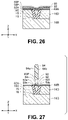
- FIG. 26 is a cross-sectional view showing a step that follows the step shown in FIG. 25 .
- FIG. 27 is a cross-sectional view showing a step that follows the step shown in FIG. 26 .
- FIG. 28 is a front view showing essential parts of a magnetic head according to a fourth embodiment of the invention.
- FIG. 29 is a cross-sectional view showing a step of a manufacturing method for the magnetic head according to the fourth embodiment of the invention.
- FIG. 30 is a cross-sectional view showing a step that follows the step shown in FIG. 29 .
- FIG. 31 is a cross-sectional view showing a step that follows the step shown in FIG. 30 .
- FIG. 32 is a cross-sectional view showing a step that follows the step shown in FIG. 31 .
- FIG. 33 is a cross-sectional view showing a step that follows the step shown in FIG. 32 .
- FIG. 34 is a cross-sectional view showing a step that follows the step shown in FIG. 33 .
- FIG. 5 is a cross-sectional view showing a configuration of the magnetic head.
- FIG. 6 is a front view showing a medium facing surface of the magnetic head.
- FIG. 7 is a plan view showing a lower coil portion of the magnetic head.
- FIG. 8 is a plan view showing an upper coil portion of the magnetic head.
- the magnetic head 100 according to the present embodiment is one intended for perpendicular magnetic recording.
- the magnetic head 100 according to the present embodiment is for use with, e.g., a magnetic disk drive, and is incorporated in a slider configured to fly over the surface of a rotating recording medium 90 .
- the slider has a medium facing surface 80 configured to face the recording medium 90 .
- the medium facing surface 80 has an air inflow end (a leading end) and an air outflow end (a trailing end). An airflow that comes from the leading end into the space between the medium facing surface 80 and the recording medium 90 causes the slider to slightly fly over the surface of the recording medium 90 .
- the X direction is the direction across the tracks of the recording medium 90 , i.e., the track width direction.
- the Y direction is a direction perpendicular to the medium facing surface 80 .
- the Z direction is the direction of travel of the recording medium 90 as viewed from the slider.
- the X, Y, and Z directions are orthogonal to one another.
- the magnetic head 100 has the aforementioned medium facing surface 80 .
- the magnetic head 100 includes: a substrate 1 formed of a ceramic material such as aluminum oxide-titanium carbide (Al 2 O 3 —TiC) and having a top surface 1 a ; an insulating layer 2 formed of an insulating material such as alumina (Al 2 O 3 ) and disposed on the top surface 1 a of the substrate 1 ; a first read shield layer 3 formed of a magnetic material and disposed on the insulating layer 2 ; a magnetoresistive (MR) element 5 as a read element disposed on the first read shield layer 3 ; an insulating layer 6 formed of an insulating material and disposed around the MR element 5 ; and a second read shield layer 7 formed of a magnetic material and disposed on the MR element 5 and the insulating layer 6 .
- a substrate 1 formed of a ceramic material such as aluminum oxide-titanium carbide (Al 2 O 3 —TiC) and having
- the MR element 5 may be an element formed of a magneto-sensitive film that exhibits a magnetoresistive effect, such as an anisotropic magnetoresistive (AMR) element, a giant magnetoresistive (GMR) element, or a tunneling magnetoresistive (TMR) element.
- AMR anisotropic magnetoresistive
- GMR giant magnetoresistive
- TMR tunneling magnetoresistive
- the GMR element may be of either the current-in-plane (CIP) type in which a current for use in magnetic signal detection is fed in a direction generally parallel to the plane of layers constituting the GMR element or the current-perpendicular-to-plane (CPP) type in which the current for use in magnetic signal detection is fed in a direction generally perpendicular to the plane of the layers constituting the GMR element.
- CIP current-in-plane
- CPP current-perpendicular-to-plane
- the parts from the first read shield layer 3 to the second read shield layer 7 constitute a read head unit 8 .
- the magnetic head 100 further includes: a nonmagnetic layer 71 formed of a nonmagnetic material and disposed on the second read shield layer 7 ; a middle shield layer 72 formed of a magnetic material and disposed on the nonmagnetic layer 71 ; a nonmagnetic layer 73 formed of a nonmagnetic material and disposed on the middle shield layer 72 ; and a write head unit 9 disposed on the nonmagnetic layer 73 .
- the middle shield layer 72 has a function of shielding the MR element 5 from magnetic fields generated in the write head unit 9 .
- the nonmagnetic layers 71 and 73 are formed of alumina, for example.
- the write head unit 9 includes a coil, a main pole 15 , and a write shield 16 .
- the coil generates a magnetic field corresponding to data to be written on the recording medium 90 .
- the coil includes an upper coil portion 20 and a lower coil portion 10 .
- Each of the upper coil portion 20 and the lower coil portion 10 is formed of a conductive material such as copper.
- the upper coil portion 20 and the lower coil portion 10 are connected in series or in parallel.
- the main pole 15 has an end face 15 a located in the medium facing surface 80 , and is configured to pass a magnetic flux corresponding to the magnetic field generated by the coil and to generate a write magnetic field for writing data on the recording medium 90 by means of a perpendicular magnetic recording system.
- FIG. 5 shows a cross section that intersects the end face 15 a of the main pole 15 and that is perpendicular to the medium facing surface 80 and to the top surface 1 a of the substrate 1 .
- the write shield 16 includes a trailing shield 16 A, a leading shield 16 B, a first side shield 16 C, and a second side shield 16 D.
- the trailing shield 16 A is located forward relative to the main pole 15 in the direction of travel of the recording medium 90 (the Z direction). Being located forward relative to the main pole 15 in the direction of travel of the recording medium 90 refers to being located farther from the top surface 1 a of the substrate 1 than the main pole 15 .
- the leading shield 16 B is located backward relative to the main pole 15 in the direction of travel of the recording medium 90 . Being located backward relative to the main pole 15 in the direction of travel of the recording medium 90 refers to being located closer to the top surface 1 a of the substrate 1 than the main pole 15 .
- the first and second side shields 16 C and 16 D are located farther from the top surface 1 a of the substrate 1 than the leading shield 16 B, opposed to each other in the track width direction (the X direction) with the main pole 15 therebetween, and magnetically couple the trailing shield 16 A and the leading shield 16 B.
- the trailing shield 16 A has a front end face 16 Aa located in the medium facing surface 80 .
- the leading shield 16 B has a front end face 16 Ba located in the medium facing surface 80 .
- the first side shield 16 C has a front end face 16 Ca located in the medium facing surface 80 .
- the second side shield 16 D has a front end face 16 Da located in the medium facing surface 80 .
- the front end face 16 Aa is located forward relative to the end face 15 a of the main pole 15 in the direction of travel of the recording medium 90 .
- the front end face 16 Ba is located backward relative to the end face 15 a of the main pole 15 in the direction of travel of the recording medium 90 .
- the front end faces 16 Ca and 16 Da are opposed to each other in the track width direction with the end face 15 a of the main pole 15 therebetween.
- the front end faces 16 Aa, 16 Ba, 16 Ca, and 16 Da are arranged to surround the end face 15 a of the main pole 15 .
- the write shield 16 is formed of a magnetic material.
- CoFeN, CoNiFe, FeNi, or CoFe may be used as the material of the write shield 16 .
- the write head unit 9 further includes a spin torque oscillator 60 .
- the spin torque oscillator 60 is located between the main pole 15 and the trailing shield 16 A in the vicinity of the medium facing surface 80 and electrically connected to the main pole 15 and the trailing shield 16 A.
- the spin torque oscillator 60 may be an element configured to generate a microwave magnetic field or an element configured to adjust a magnetic permeability between the main pole 15 and the trailing shield 16 A. The configuration of the spin torque oscillator 60 will be described in detail later.
- the write head unit 9 further includes an upper return path section 40 and a lower return path section 30 .
- Both the upper return path section 40 and the lower return path section 30 are formed of a magnetic material.
- CoFeN, CoNiFe, FeNi, or CoFe may be used as the material of the upper return path section 40 and the lower return path section 30 .
- the upper return path section 40 is located forward relative to the main pole 15 in the direction of travel of the recording medium 90 , and connects part of the main pole 15 located away from the medium facing surface 80 to the write shield 16 , thereby magnetically coupling the main pole 15 to the write shield 16 .
- the upper return path section 40 and the main pole 15 define an upper space USP (see FIG. 8 ) for a portion of the coil to pass through.
- the lower return path section 30 is located backward relative to the main pole 15 in the direction of travel of the recording medium 90 , and connects part of the main pole 15 located away from the medium facing surface 80 to the write shield 16 , thereby magnetically coupling the main pole 15 to the write shield 16 .
- the lower return path section 30 and the main pole 15 define a lower space LSP (see FIG. 7 ) for a portion of the coil to pass through.
- the lower return path section 30 includes coupling portions 31 , 32 , 33 , 34 , and 35 .
- the coupling portion 31 is disposed on the nonmagnetic layer 73 .
- the coupling portions 32 and 33 are both disposed on the coupling portion 31 .
- the coupling portion 32 is located near the medium facing surface 80 .
- the coupling portion 33 is located farther from the medium facing surface 80 than the coupling portion 32 .
- the coupling portions 31 and 32 have their respective end faces that face toward the medium facing surface 80 and that are each located at a distance from the medium facing surface 80 .
- the write head unit 9 further includes: an insulating layer 51 formed of an insulating material, disposed on the nonmagnetic layer 73 and surrounding the coupling portion 31 ; an insulating film 52 formed of an insulating material and isolating the lower coil portion 10 from the coupling portions 31 to 33 ; and an insulating layer 53 formed of an insulating material and disposed around the lower coil portion 10 and the coupling portion 32 .
- the coupling portion 34 is embedded in the coupling portion 32 and the insulating layer 53 .
- the coupling portion 34 has an end face located in the medium facing surface 80 .
- the top surfaces of the lower coil portion 10 , the coupling portions 32 to 34 , the insulating film 52 and the insulating layer 53 are even with each other.
- the insulating layers 51 and 53 and the insulating film 52 are formed of alumina, for example.
- the leading shield 16 B lies on a part of the top surface of the coupling portion 34 .
- the write head unit 9 further includes an insulating layer 54 formed of an insulating material.
- the insulating layer 54 lies on another part of the top surface of the coupling portion 34 and on the top surfaces of the lower coil portion 10 , the coupling portions 32 and 33 , the insulating film 52 and the insulating layer 53 .
- the coupling portion 35 lies over the coupling portion 33 with the insulating layer 53 interposed therebetween. Note that the coupling portions 33 and 35 magnetically couple to each other even with the insulating layer 53 interposed between the coupling portions 33 and 35 .
- the insulating layer 54 is formed of alumina, for example.
- the write head unit 9 further includes a nonmagnetic layer 55 formed of a nonmagnetic material.
- the nonmagnetic layer 55 lies on the insulating layer 54 and surrounds the leading shield 16 B and the coupling portion 35 .
- the nonmagnetic layer 55 is formed of alumina or silicon oxide (SiO 2 ), for example.
- the first and second side shields 16 C and 16 D are disposed on the leading shield 16 B.
- the main pole 15 has the end face 15 a , and also a top surface 15 T (see FIG. 5 ) farthest from the top surface 1 a of the substrate 1 , a bottom end 15 L (see FIG. 5 ) opposite to the top surface 15 T, and a first side surface and a second side surface (see FIG. 6 to FIG. 8 ) opposite to each other in the track width direction (the X direction).
- the first side shield 16 C has a first sidewall opposed to a portion of the first side surface of the main pole 15 located near the medium facing surface 80 .
- the second side shield 16 D has a second sidewall opposed to a portion of the second side surface of the main pole 15 located near the medium facing surface 80 .
- the write head unit 9 further includes a first gap layer 18 formed of a nonmagnetic material.
- the first gap layer 18 is disposed to extend along the first and second sidewalls of the first and second side shields 16 C and 16 D, the top surface of the leading shield 16 B, and the top surface of the nonmagnetic layer 55 .
- An example of the nonmagnetic material used to form the first gap layer 18 is an insulating material such as alumina.
- the first gap layer 18 is interposed between a portion of the bottom end 15 L of the main pole 15 and the top surfaces of the leading shield 16 B and the nonmagnetic layer 55 . As shown in FIG. 6 , the first gap layer 18 is interposed also between the first side surface of the main pole 15 and the first sidewall of the first side shield 16 C, and between the second side surface of the main pole 15 and the second sidewall of the second side shield 16 D.
- the main pole 15 is formed of a ferromagnetic material containing one or more elements selected from Ni, Fe, and Co, such as FeNi, CoNiFe, or CoFe. The shape of the main pole 15 will be described in detail later.
- the write head unit 9 further includes a first nonmagnetic layer (not shown) formed of a nonmagnetic material and disposed around the main pole 15 and the first and second side shields 16 C and 16 D.
- a first nonmagnetic layer (not shown) formed of a nonmagnetic material and disposed around the main pole 15 and the first and second side shields 16 C and 16 D.
- An example of the nonmagnetic material used to form the first nonmagnetic layer is an insulating material such as alumina.
- the write head unit 9 further includes a buffer layer 59 formed of a nonmagnetic conductive material. Note that the buffer layer 59 is shown in FIG. 1 to FIG. 4 to be described later.
- the buffer layer 59 is located near the medium facing surface 80 , lies on the top surface 15 T of the main pole 15 and is in contact with the top surface 15 T of the main pole 15 .
- the spin torque oscillator 60 lies on the buffer layer 59 .
- the buffer layer 59 is formed of, for example, one of Ta, Al, Ti, Mn, Ni, Zn, Zr, Nb, Mo, Ru, Rh, Pd, Ag, Hf, W, Ir, Pt, and Au, or an alloy composed of two or more of these elements.
- the write head unit 9 further includes: a nonmagnetic layer 61 formed of a nonmagnetic material and disposed on a first portion of the top surface 15 T of the main pole 15 , the first portion being located away from the buffer layer 59 and the spin torque oscillator 60 ; and an insulating layer 63 formed of an insulating material and disposed to cover the main pole 15 and the nonmagnetic layer 61 .
- the nonmagnetic layer 61 is formed of silicon oxide, for example.
- the insulating layer 63 is formed of alumina, for example.
- the write head unit 9 further includes first and second gap films 19 A and 19 B formed of a nonmagnetic material. As shown in FIG. 6 , the first and second gap films 19 A and 19 B are opposed to each other in the track width direction (X direction) with the buffer layer 59 and the spin torque oscillator 60 therebetween.
- An example of the nonmagnetic material constituting the first and second gap films 19 A and 19 B is an insulating material such as alumina.
- the write head unit 9 further includes first and second guard films 62 A and 62 B formed of a nonmagnetic material.
- the first and second guard films 62 A and 62 B are shown in FIG. 2 to be described below.
- the first guard film 62 A lies on the first side shield 16 C and the first gap layer 18 .
- the second guard film 62 B lies on the second side shield 16 D and the first gap layer 18 .
- the first gap film 19 A lies on the first guard film 62 A.
- the second gap film 19 B lies on the second guard film 62 B.
- Examples of the nonmagnetic material constituting the first and second guard films 62 A and 62 B include a nonmagnetic insulating material such as alumina, and a nonmagnetic metal material such as Ru.
- the trailing shield 16 A is disposed on the first and second side shields 16 C and 16 D, the first and second gap films 19 A and 19 B, the spin torque oscillator 60 and the insulating layer 63 , and in contact with the top surfaces of the first and second side shields 16 C and 16 D, the first and second gap films 19 A and 19 B, the spin torque oscillator 60 and the insulating layer 63 .
- a portion of the front end face 16 Aa of the trailing shield 16 A is spaced a predetermined distance away from the end face 15 a of the main pole 15 .
- the predetermined distance is preferably in the range of 5 to 60 nm, and may be 30 to 60 nm, for example.
- the upper return path section 40 includes coupling portions 41 and 42 .
- the coupling portion 41 lies on a second portion of the top surface 15 T of the main pole 15 , the second portion being located away from the medium facing surface 80 .
- the second portion of the top surface 15 T of the main pole 15 is located farther from the medium facing surface 80 than the first portion of the top surface 15 T of the main pole 15 .
- the write head unit 9 further includes: an insulating film 64 formed of an insulating material and isolating at least part of the upper coil portion 20 from the trailing shield 16 A, the coupling portion 41 , and the insulating layer 63 ; and a second nonmagnetic layer (not shown) formed of a nonmagnetic material and disposed around the trailing shield 16 A and the upper coil portion 20 .
- the insulating film 64 is formed of alumina, for example.
- An example of the nonmagnetic material used to form the second nonmagnetic layer is an insulating material such as alumina.
- the write head unit 9 further includes an insulating layer 65 formed of an insulating material and disposed on the upper coil portion 20 , the coupling portion 41 and the insulating film 64 .
- the insulating layer 65 includes a first portion lying on the upper coil portion 20 and a second portion lying on the coupling portion 41 . The second portion is smaller in maximum thickness (maximum dimension in the Z direction) than the first portion.
- the insulating layer 65 is formed of alumina, for example.
- the coupling portion 42 is disposed on the trailing shield 16 A and the insulating layer 65 .
- the coupling portion 42 has an end face located in the medium facing surface 80 .
- the coupling portion 42 includes a first portion lying on the trailing shield 16 A, a second portion lying over the coupling portion 41 with the insulating layer 65 interposed therebetween, and a third portion connecting the first and second portions. Note that the coupling portions 41 and 42 magnetically couple to each other even with the insulating layer 65 interposed between the coupling portion 41 and the second portion of the coupling portion 42 .
- the magnetic head 100 further includes a protective layer 70 formed of a nonmagnetic material and disposed to cover the write head unit 9 .
- the protective layer 70 is formed of, e.g., an inorganic insulating material such as alumina.
- the magnetic head 100 includes the medium facing surface 80 , the read head unit 8 , and the write head unit 9 .
- the read head unit 8 and the write head unit 9 are stacked on the substrate 1 .
- the write head unit 9 is located forward relative to the read head unit 8 in the direction of travel of the recording medium 90 (the Z direction).
- the write head unit 9 includes the coil including the upper coil portion 20 and the lower coil portion 10 , the main pole 15 , the write shield 16 , the first gap layer 18 , the first and second gap films 19 A and 19 B, the buffer layer 59 , the spin torque oscillator 60 , and the first and second guard films 62 A and 62 B.
- the coil, the main pole 15 , the write shield 16 , the first gap layer 18 , the second gap layer 19 , the buffer layer 59 , the spin torque oscillator 60 , and the first and second guard films 62 A and 62 B are disposed above the top surface 1 a of the substrate 1 .
- the write shield 16 includes the trailing shield 16 A, the leading shield 16 B, and the first and second side shields 16 C and 16 D.
- the write head unit 9 further includes the upper return path section 40 and the lower return path section 30 .
- the upper return path section 40 includes the coupling portions 41 and 42 .
- the lower return path section 30 includes the coupling portions 31 , 32 , 33 , 34 , and 35 .
- the write shield 16 captures a disturbance magnetic field applied to the magnetic head 100 from outside the magnetic head 100 . This makes it possible to prevent erroneous writing on the recording medium 90 that would be caused by the disturbance magnetic field being intensively captured into the main pole 15 .
- the write shield 16 further has a function of capturing a magnetic flux that is generated from the end face 15 a of the main pole 15 and spreads in directions other than the direction perpendicular to the plane of the recording medium 90 , and thereby preventing the magnetic flux from reaching the recording medium 90 .
- the write shield 16 , the upper return path section 40 and the lower return path section 30 have a function of causing a magnetic flux that has been generated from the end face 15 a of the main pole 15 and has magnetized a portion of the recording medium 90 to flow back.
- the spin torque oscillator 60 is electrically connected to the main pole 15 and the trailing shield 16 A.
- the spin torque oscillator 60 is electrically connected to the main pole 15 via the buffer layer 59 .
- the magnetic head 100 further includes: two terminals 81 and 82 connected to a power source (not shown); wiring 83 for electrically connecting the terminal 81 and the main pole 15 ; and wiring 84 for electrically connecting the terminal 82 and the coupling portion 42 .
- the trailing shield 16 A is electrically connected to the coupling portion 42 .
- a current for operating the spin torque oscillator 60 which will hereinafter be referred to as a driving current, is supplied via the terminals 81 and 82 .
- the driving current flows through the main pole 15 , the buffer layer 59 , the spin torque oscillator 60 , the trailing shield 16 A, and the coupling portion 42 in this order.
- FIG. 4 is a front view showing the spin torque oscillator 60 .
- the spin torque oscillator 60 shown in FIG. 4 is one configured to generate a microwave magnetic field.
- This spin torque oscillator 60 includes a magnetic-field generating layer 601 , a nonmagnetic layer 602 , and a spin injection layer 603 stacked in this order, from closest to farthest from the buffer layer 59 .
- the magnetic-field generating layer 601 is formed of a material whose magnetization direction is parallel or almost parallel to the film plane when no driving current flows.
- the magnetic-field generating layer 601 may be a magnetic layer formed of one of FeCo, FeCoAl, FeCoSi, FeCoB, and FeNi, a layered film composed of alternately stacked layers of FeCo and Ni, or a layered film composed of alternately stacked layers of Fe and Co.
- the nonmagnetic layer 602 is formed of a material having high spin permeability.
- the nonmagnetic layer 602 may be a nonmagnetic metal layer formed of one of Ag, Au, Cr, and Al, or a tunnel barrier layer formed of MgO or Al 2 O 3 .
- the spin injection layer 603 is formed of a material having magnetic anisotropy in a direction perpendicular to the film plane.
- the spin injection layer 603 may be a layered film composed of alternately stacked layers of CoFe and Ni, a layered film composed of alternately stacked layers of Co and Pt, a layered film composed of alternately stacked layers of Co and Pd, or an alloy layer formed of one of CoPt, FePt, and MnGa.
- the spin torque oscillator 60 may further include a protective layer disposed on the spin injection layer 603 .
- the protective layer is formed of a nonmagnetic metal material.
- the protective layer is formed of one of Ta, Al, Ti, Mn, Fe, Co, Ni, Cu, Zn, Zr, Nb, Mo, Ru, Rh, Pd, Ag, Hf, W, Ir, Pt, and Au, or an alloy composed of two or more of these elements.
- the lower coil portion 10 has a coil connection 10 E electrically connected to the upper coil portion 20 .
- the upper coil portion 20 has a coil connection 20 S electrically connected to the coil connection 10 E of the lower coil portion 10 .
- the coil connection 20 S is electrically connected to the coil connection 10 E via a first and a second connection layer of columnar shape (not shown) that penetrate a plurality of layers interposed between the upper coil portion 20 and the lower coil portion 10 .
- the first and second connection layers are stacked in this order on the coil connection 10 E.
- the coil connection 20 S lies on the second connection layer.
- the first and second connection layers are formed of a conductive material such as copper.
- the upper coil portion 20 and the lower coil portion 10 are connected in series.
- FIG. 1 is a perspective view showing essential parts of the magnetic head 100 .
- FIG. 2 is a front view showing essential parts of the magnetic head 100 .
- FIG. 3 is a cross-sectional view showing essential parts of the magnetic head 100 .
- the main pole 15 includes a track width defining portion 15 A having the end face 15 a and an end opposite thereto, and a wide portion 15 B connected to the end of the track width defining portion 15 A.
- the main pole 15 has the top surface 15 T, the bottom end 15 L, the first side surface, and the second side surface.
- a width in the track width direction (the X direction) will be simply referred to as a width.
- the width of the top surface 15 T is greater in the wide portion 15 B than in the track width defining portion 15 A.
- the width of the top surface 15 T in the track width defining portion 15 A gradually increases with increasing distance from the medium facing surface 80 , and then becomes constant.
- the top surface 15 T includes an inclined portion 15 T 1 and a flat portion 15 T 2 , the inclined portion 15 T 1 being closer to the medium facing surface 80 than the flat portion 15 T 2 .
- the inclined portion 15 T 1 has a first end closest to the medium facing surface 80 and a second end opposite thereto.
- the flat portion 15 T 2 is connected to the second end of the inclined portion 15 T 1 .
- the inclined portion 15 T 1 is inclined such that the second end is located forward relative to the first end in the direction of travel of the recording medium 90 (the Z direction).
- the flat portion 15 T 2 extends substantially in a direction perpendicular to the medium facing surface 80 (the Y direction).
- the bottom end 15 L includes a first inclined portion and a first flat portion, the first inclined portion being closer to the medium facing surface 80 than the first flat portion.
- the first inclined portion has a third end located in the medium facing surface 80 , and a fourth end opposite thereto.
- the first inclined portion may be an edge formed by two intersecting surfaces, or may be a surface connecting two surfaces to each other.
- the first flat portion is a surface connected to the fourth end of the first inclined portion.
- the first inclined portion is inclined such that the fourth end is located backward relative to the third end in the direction of travel of the recording medium 90 (the Z direction).
- the first flat portion extends substantially in a direction perpendicular to the medium facing surface 80 (the Y direction).
- the bottom end 15 L further includes a second inclined portion and a second flat portion.
- the second inclined portion is a surface connected to an end of the first flat portion opposite from the first inclined portion.
- the second flat portion is a surface connected to an end of the second inclined portion opposite from the first flat portion.
- the second inclined portion is inclined in a manner similar to that in which the first inclined portion is inclined.
- the second flat portion extends substantially in a direction perpendicular to the medium facing surface 80 (the Y direction), like the first flat portion.
- the end face 15 a of the main pole 15 has a top edge farthest from the top surface 1 a of the substrate 1 , a first side edge connected to one end of the top edge, and a second side edge connected to the other end of the top edge.
- the top edge is in contact with the buffer layer 59 .
- the top edge defines the track width.
- the position of an end of a recording bit to be recorded on the recording medium 90 is determined by the position of the top edge.
- the width in the track width direction of the end face 15 a of the main pole 15 decreases with increasing distance from the top edge, i.e., with decreasing distance to the top surface 1 a of the substrate 1 .
- Each of the first side edge and the second side edge forms an angle in the range of, for example, 7° to 17°, preferably 10° to 15°, with respect to a direction perpendicular to the top surface 1 a of the substrate 1 .
- the top edge has a length in the range of 0.05 to 0.20 ⁇ m, for example.
- the spin torque oscillator 60 has a front end face 60 a facing the medium facing surface 80 , a rear end face 60 b farthest from the medium facing surface 80 , a top surface 60 c farthest from the top surface 1 a of the substrate 1 , a bottom surface 60 d closest to the top surface 1 a of the substrate 1 , and a first side surface 60 e and a second side surface 60 f opposite to each other in the track width direction (the X direction).
- the front end face 60 a is located in the medium facing surface 80 .
- the top surface 60 c is in contact with the trailing shield 16 A.
- the bottom surface 60 d is in contact with the buffer layer 59 .
- the first and second side surfaces 60 e and 60 f are perpendicular or substantially perpendicular to the top surface 1 a (see FIG. 5 and FIG. 6 ) of the substrate 1 .
- the first side surface 60 e and the second side surface 60 f respectively form a first angle and a second angle with respect to a direction perpendicular to the top surface 1 a of the substrate 1 .
- the first and second angles each are preferably in the range of 0° to 15°, more preferably in the range of 0° to 10°.
- the buffer layer 59 has an end face located in the medium facing surface 80 , a top surface farthest from the top surface 1 a of the substrate 1 , a bottom surface closest to the top surface 1 a of the substrate 1 , and a third side surface 59 a and a fourth side surface 59 b opposite to each other in the track width direction (the X direction).
- the top surface of the buffer layer 59 is in contact with the bottom surface 60 d of the spin torque oscillator 60 .
- the bottom surface of the buffer layer 59 is in contact with the inclined portion 15 T 1 of the top surface 15 T of the main pole 15 .
- the third side surface 59 a of the buffer layer 59 is contiguous with the first side surface 60 e of the spin torque oscillator 60 .
- the third side surface 59 a forms a third angle greater than the aforementioned first angle with respect to the direction perpendicular to the top surface 1 a of the substrate 1 .
- the third angle falls within the range of, e.g., 10° to 70°. If the first angle is 10°, the third angle is greater than 10°.
- the fourth side surface 59 b of the buffer layer 59 is contiguous with the second side surface 60 f of the spin torque oscillator 60 .
- the fourth side surface 59 b forms a fourth angle greater than the aforementioned second angle with respect to the direction perpendicular to the top surface 1 a of the substrate 1 .
- the fourth angle falls within the range of, e.g., 10° to 70°. If the second angle is 10°, the fourth angle is greater than 10°.
- the trailing shield 16 A includes a seed layer 16 A 1 and a magnetic layer 16 A 2 located on the seed layer 16 A 1 .
- the seed layer 16 A 1 has an end face 16 A 1 a located in the medium facing surface 80 .
- the magnetic layer 16 A 2 has an end face 16 A 2 a located in the medium facing surface 80 .
- the front end face 16 Aa of the trailing shield 16 A includes the end faces 16 A 1 a and 16 A 2 a.
- the first gap film 19 A and the first guard film 62 A are interposed between the trailing shield 16 A and the first side shield 16 C near the spin torque oscillator 60 .
- the first guard film 62 A is interposed between the first gap film 19 A and the first side shield 16 C.
- the first gap film 19 A and the first guard film 62 A are not interposed between the trailing shield 16 A and the first side shield 16 C, and the bottom surface of the trailing shield 16 A (bottom surface of the seed layer 16 A 1 ) and the top surface of the first side shield 16 C are in contact with each other.
- the second gap film 19 B and the second guard film 62 B are interposed between the trailing shield 16 A and the second side shield 16 D near the spin torque oscillator 60 .
- the second guard film 62 B is interposed between the second gap film 19 B and the second side shield 16 D.
- the second gap film 19 B and the second guard film 62 B are not interposed between the trailing shield 16 A and the second side shield 16 D, and the bottom surface of the trailing shield 16 A (bottom surface of the seed layer 16 A 1 ) and the top surface of the second side shield 16 D are in contact with each other.
- the distance between the trailing shield 16 A and the first side shield 16 C in the medium facing surface 80 and the distance between the trailing shield 16 A and the second side shield 16 D in the medium facing surface 80 are each the same or substantially the same as the distance between the main pole 15 and the trailing shield 16 A in the medium facing surface 80 .
- the top surface 15 T of the main pole 15 , the top surface of the first side shield 16 C, and the top surface of the second side shield 16 D are each located at the same or substantially the same positions in the medium facing surface 80 .
- the top surface 60 c of the spin torque oscillator 60 , the top surface of the first gap film 19 A, and the top surface of the second gap film 19 B are located at the same or substantially the same positions in the medium facing surface 80 .
- the first and second gap films 19 A and 19 B are in contact with the spin torque oscillator 60 .
- the first and second guard films 62 A and 62 B are not in contact with the spin torque oscillator 60 .
- the manufacturing method for the magnetic head 100 according to the present embodiment starts with forming the insulating layer 2 , the first read shield layer 3 , and the MR element 5 in this order on the substrate 1 , as shown in FIG. 5 and FIG. 6 .
- the insulating layer 6 is formed around the MR element 5 .
- the second read shield layer 7 , the nonmagnetic layer 71 , the middle shield layer 72 , and the nonmagnetic layer 73 are then formed in this order over the MR element 5 and the insulating layer 6 .
- the coupling portion 31 is formed on the nonmagnetic layer 73 by frame plating, for example.
- the insulating layer 51 is formed over the entire top surface of the stack.
- the insulating layer 51 is then polished by, for example, chemical mechanical polishing (hereinafter referred to as CMP), until the coupling portion 31 is exposed.
- CMP chemical mechanical polishing
- the coupling portions 32 and 33 are formed on the coupling portion 31 by frame plating, for example.
- the insulating film 52 is then formed over the entire top surface of the stack.
- the lower coil portion 10 is formed by frame plating, for example.
- the insulating layer 53 is then formed over the entire top surface of the stack.
- the insulating film 52 and the insulating layer 53 are then polished by, for example, CMP, until the lower coil portion 10 and the coupling portions 32 and 33 are exposed.
- the coupling portion 32 and the insulating layer 53 are etched to form therein an accommodation part to accommodate the coupling portion 34 .
- the coupling portion 34 is formed to be accommodated in the accommodation part.
- the insulating layer 54 is then formed over the entire top surface of the stack.
- the insulating layer 54 is selectively etched to form therein a first opening for exposing the top surface of the coupling portion 34 and a second opening for exposing the coil connection 10 E (see FIG. 7 ) of the lower coil portion 10 .
- the leading shield 16 B is formed on the coupling portion 34 at the position of the first opening
- the coupling portion 35 is formed on a portion of the insulating layer 54 covering the top surface of the coupling portion 33
- the first connection layer (not shown) is formed on the coil connection 10 E at the position of the second opening, by performing frame plating, for example.
- the nonmagnetic layer 55 is formed over the entire top surface of the stack.
- the nonmagnetic layer 55 is then polished by, for example, CMP, until the leading shield 16 B, the coupling portion 35 and the first connection layer are exposed.
- the leading shield 16 B and the nonmagnetic layer 55 are taper-etched in part by, for example, ion beam etching (hereinafter referred to as IBE) so as to provide the top surface of the leading shield 16 B with a portion to be opposed to the first inclined portion (see FIG. 2 ) of the bottom end 15 L of the main pole 15 to be formed later, and provide the top surface of the nonmagnetic layer 55 with a portion to be opposed to the second inclined portion (see FIG. 5 ) of the bottom end 15 L of the main pole 15 to be formed later.
- the coupling portion 35 and the first connection layer are also etched in part by this etching.
- the first and second side shields 16 C and 16 D are formed on the leading shield 16 B by, for example, frame plating.
- the first gap layer 18 is then formed to cover the leading shield 16 B and the first and second side shields 16 C and 16 D.
- the first gap layer 18 is formed by atomic layer deposition (hereinafter referred to as ALD), for example.
- ALD atomic layer deposition
- the first gap layer 18 is then selectively etched to form therein an opening for exposing the top surface of the coupling portion 35 , and an opening for exposing the top surface of the first connection layer.
- an initial main pole, which becomes the main pole 15 later, and the second connection layer are formed by frame plating, for example.
- the initial main pole and the second connection layer are formed such that their top surfaces are higher in level than portions of the first gap layer 18 that are located on the first and second side shields 16 C and 16 D.
- the first nonmagnetic layer (not shown) is formed over the entire top surface of the stack.
- the initial main pole, the second connection layer, the first gap layer 18 , and the first nonmagnetic layer are then polished by, for example, CMP until the first and second side shields 16 C and 16 D are exposed.
- the nonmagnetic layer 61 is formed on the initial main pole.
- the initial main pole and the nonmagnetic layer 61 are then taper-etched by, e.g, IBE so as to provide the initial main pole with the inclined portion 15 T 1 (see FIG. 1 and FIG. 3 ) of the top surface 15 T of the main pole 15 . This makes the initial main pole into the main pole 15 .
- the first and second side shields 16 C and 16 D, the first gap layer 18 , and the first nonmagnetic layer are also etched in part by this etching.
- FIG. 9 to FIG. 17 each show a stack of layers formed in the process of manufacturing the magnetic head 100 .
- FIG. 9 to FIG. 17 omit the illustration of portions that are closer to the substrate 1 relative to the leading shield 16 B.
- FIG. 9 to FIG. 17 each show a cross section of the stack taken at the position where the medium facing surface 80 is to be formed.
- FIG. 9 shows a step following the formation of the main pole 15 .
- a mask 91 is initially formed on the stack including the main pole 15 .
- the mask 91 has two openings for exposing the top surfaces of the respective first and second side shields 16 C and 16 D.
- the mask 91 includes a lower layer lying on the stack and an upper layer lying on the lower layer.
- the upper layer is formed of a photoresist patterned by photolithography.
- the lower layer is formed of, for example, a material that dissolves in a developing solution used in patterning the upper layer.
- a gap develops between the stack and the mask 91 in the cross section taken at the position where the medium facing surface 80 is to be formed. Note that even if the foregoing portion of the lower layer is removed, the mask 91 will not peel away since the lower layer remains between the stack and the upper layer except in and near the cross section taken at the position where the medium facing surface 80 is to be formed.
- FIG. 10 shows the next step.
- a nonmagnetic film of a nonmagnetic material is initially formed over the entire top surface of the stack.
- the portion of the nonmagnetic film formed on the first side shield 16 C makes the first guard film 62 A.
- the portion of the nonmagnetic film formed on the second side shield 16 D makes the second guard film 62 B.
- the mask 91 is then removed.
- FIG. 11 shows the next step.
- an initial buffer layer 59 P which becomes the buffer layer 59 later, is formed on the stack.
- a layered film 60 P which becomes the spin torque oscillator 60 later, is formed on the initial buffer layer 59 P.
- the spin torque oscillator 60 is composed of a plurality of layers.
- the layered film 60 P includes all the layers to constitute the spin torque oscillator 60 .
- a nonmagnetic metal layer 92 of Ru is then formed on the layered film 60 P.
- a protective layer 93 is formed on the nonmagnetic metal layer 92 .
- the protective layer 93 is what is called a hard mask, and is formed of an inorganic material. In the present embodiment, specifically, the protective layer 93 is formed of carbon.
- the protective layer 93 has a thickness in the range of 10 to 30 nm, for example.
- FIG. 12 shows the next step.
- a mask 94 is formed on the protective layer 93 .
- the mask 94 has a first sidewall 94 a defining the shape and the position of each of the first side surface 60 e of the spin torque oscillator 60 and the third side surface 59 a of the buffer layer 59 , and a second sidewall 94 b defining the shape and the position of each of the second side surface 60 f of the spin torque oscillator 60 and the fourth side surface 59 b of the buffer layer 59 .
- the mask 94 includes a lower layer and an upper layer. The lower layer is located on the protective layer 93 . As shown in FIG. 12 , a gap develops between the protective layer 93 and the mask 94 in the cross section taken at the position where the medium facing surface 80 is to be formed.
- part of the protective layer 93 is then etched by using the mask 94 .
- This etching is performed by using reactive ion etching (hereinafter, referred to as RIE), for example.
- RIE reactive ion etching
- the protective layer 93 is of carbon
- a gas containing O 2 is used as an etching gas.
- the nonmagnetic metal layer 92 functions as an etching stopper to stop etching when the protective layer 93 is etched by RIE.
- the layered film 60 P, the initial buffer layer 59 P, and the nonmagnetic metal layer 92 are each etched in part by using the mask 94 and the protective layer 93 as etching masks.
- This etching is performed by using IBE, for example.
- the etching etches part of each of the layered film 60 P and the initial buffer layer 59 P so that the first and second side surfaces 60 e and 60 f of the spin torque oscillator 60 are formed on the layered film 60 P, and the third and fourth side surfaces 59 a and 59 b of the buffer layer 59 are formed on the initial buffer layer 59 P.
- Providing the initial buffer layer 59 P with the third and fourth side surfaces 59 a and 59 b makes the initial buffer layer 59 P into the buffer layer 59 .
- the etching is performed until the first and second guard films 62 A and 62 B are exposed.
- the first and second guard films 62 A and 62 B function as an etching stopper, and protect the first and second side shields 16 C and 16 D.
- FIG. 13 shows the next step.
- a nonmagnetic film of a nonmagnetic material is initially formed over the entire top surface of the stack by using, e.g., ion beam deposition with the mask 94 left unremoved.
- the nonmagnetic film is etched by, e.g., IBE to planarize the top surface of the nonmagnetic film.
- the portion of the nonmagnetic film formed on the first guard film 62 A makes the first gap film 19 A.
- the portion of the nonmagnetic film formed on the second guard film 62 B makes the second gap film 19 B.
- FIG. 14 shows the next step.
- a nonmagnetic metal layer 95 of Ru is formed over the entire top surface of the stack with the mask 94 left unremoved.
- FIG. 15 shows the next step.
- the mask 94 is initially lifted off.
- needless portions of the first and second gap films 19 A and 19 B on the protective layer 93 are removed by wet etching, for example.
- the nonmagnetic metal layer 95 has the function of protecting the portions of the first and second gap films 19 A and 19 B other than the foregoing needless portions from etching.
- FIG. 16 shows the next step.
- the nonmagnetic metal layer 95 is removed and the first and second gap films 19 A and 19 B are etched in part by IBE, for example.
- the etching is performed until the first and second gap films 19 A and 19 B each have a desired thickness.
- FIG. 17 shows the next step.
- the protective layer 93 is removed.
- the protective layer 93 is removed by ashing, for example.
- the nonmagnetic metal layer 92 is removed by IBE, for example.
- a not-shown mask is then formed on the stack.
- another part of the layered film 60 P is etched by, e.g, IBE using the mask as an etching mask so that the rear end face 60 b (see FIG. 1 and FIG. 3 ) of the spin torque oscillator 60 is formed on the layered film 60 P.
- the etching of the layered film 60 P is followed by etching of the buffer layer 59 until the inclined portion 15 T 1 of the top surface 15 T of the main pole 15 is exposed.
- the etching of the buffer layer 59 removes the portion of the buffer layer 59 not covered with the spin torque oscillator 60 .
- the insulating layer 63 (see FIG. 3 and FIG. 5 ) is formed over the entire top surface of the stack with the mask left unremoved. The mask is then lifted off.
- the first gap film 19 A and the first guard film 62 A are then selectively etched so that part of the top surface of the first side shield 16 C is exposed.
- the second gap film 19 B and the second guard film 62 B are also selectively etched so that part of the top surface of the second side shield 16 D is exposed.
- the seed layer 16 A 1 is formed on the first and second side shields 16 C and 16 D, the first and second gap films 19 A and 19 B, and the insulating layer 63 .
- the magnetic layer 16 A 2 is then formed by using the seed layer 16 A 1 as a seed and an electrode. The trailing shield 16 A is thereby completed.
- Steps following the formation of the trailing shield 16 A will be described below with reference to FIG. 5 and FIG. 6 .
- the nonmagnetic layer 61 and the insulating layer 63 are selectively etched by, for example, IBE so that the second portion of the top surface 15 T of the main pole 15 is exposed.
- the coupling portion 41 is formed on the main pole 15 by, for example, frame plating.
- the insulating film 64 is formed over the entire top surface of the stack.
- the insulating film 64 is then selectively etched to form therein an opening for exposing the top surface of the second connection layer.
- the upper coil portion 20 is formed by frame plating, for example.
- the second nonmagnetic layer (not shown) is then formed over the entire top surface of the stack.
- the insulating film 64 and the second nonmagnetic layer are then polished by, for example, CMP, until the trailing shield 16 A, the upper coil portion 20 and the coupling portion 41 are exposed.
- the insulating layer 65 is formed over the entire top surface of the stack. Then, the insulating layer 65 is selectively etched to form therein an opening for exposing the top surface of the trailing shield 16 A, and the top surface of a portion of the insulating layer 65 covering the top surface of the coupling portion 41 is also etched. The coupling portion 42 is then formed by frame plating, for example.
- the protective layer 70 is formed to cover the entire top surface of the stack. For example, the step of forming the wirings 83 and 84 is performed simultaneously with a series of steps from the step of forming the main pole 15 to the step of forming the protective layer 70 .
- wiring and a plurality of terminals including the terminals 81 and 82 are formed on the protective layer 70 , and the substrate 1 is cut near the position ABS where the medium facing surface 80 is to be formed. The cut surface is then polished into the medium facing surface 80 , and further processes such as fabrication of flying rails are performed to complete the magnetic head 100 .
- the manufacturing method for the magnetic head 100 includes a step of forming the first and second guard films 62 A and 62 B on the first and second side shields 16 C and 16 D, a step of forming the layered film 60 P to later become the spin torque oscillator 60 on the main pole 15 and the first and second guard films 62 A and 62 B, and a first etching step of etching part of the layered film 60 P until the first and second guard films 62 A and 62 B are exposed.
- the first gap film 19 A and the first guard film 62 A are interposed between the trailing shield 16 A and the first side shield 16 C near the spin torque oscillator 60 .
- the distance between the trailing shield 16 A and the first side shield 16 C near the spin torque oscillator 60 is the same as the total thickness of the first gap film 19 A and the first guard film 62 A.
- the distance between the trailing shield 16 A and the first side shield 16 C near the spin torque oscillator 60 can be controlled by controlling the thickness of each of the first gap film 19 A and the first guard film 62 A.
- the second gap film 19 B and the second guard film 62 B are interposed between the trailing shield 16 A and the second side shield 16 D near the spin torque oscillator 60 .
- the distance between the trailing shield 16 A and the second side shield 16 D near the spin torque oscillator 60 is the same as the total thickness of the second gap film 19 B and the second guard film 62 B.
- the distance between the trailing shield 16 A and the second side shield 16 D near the spin torque oscillator 60 can be controlled by controlling the thickness of each of the second gap film 19 B and the second guard film 62 B.
- the first and second guard films 62 A and 62 B can prevent the top surfaces of the first and second side shields 16 C and 16 D from being etched.
- unintended etching of the first and second side shields 16 C and 16 D can be prevented.
- the distance between the trailing shield 16 A and the first side shield 16 C near the spin torque oscillator 60 and the distance between the trailing shield 16 A and the second side shield 16 D near the spin torque oscillator 60 can be precisely controlled.
- the distances in the medium facing surface 80 can be made the same as that between the main pole 15 and the trailing shield 16 A in the medium facing surface 80 .
- the first and second side surfaces 60 e and 60 f of the spin torque oscillator 60 can be made perpendicular or substantially perpendicular to the top surface 1 a of the substrate 1 while preventing unintended etching of the first and second side shields 16 C and 16 D.
- a surface parallel or substantially parallel to the top surface 1 a of the substrate 1 will be referred to as a horizontal surface.
- a surface perpendicular or substantially perpendicular to the top surface 1 a of the substrate 1 will be referred to as a perpendicular surface.
- the horizontal surface and the perpendicular surface formed by etching are typically tapered therebetween.
- each of the first and second side surfaces 60 e and 60 f on the layered film 60 P as an entirely perpendicular surface will inevitably cause etching on the first and second side shields 16 C and 16 D.
- avoiding etching the first and second side shields 16 C and 16 D will inevitably result in the partial or entire tapering of each of the first and second side surfaces 60 e and 60 f formed on the layered film 60 P.
- the first and second side surfaces 60 e and 60 f can each be formed on the layered film 60 P as an entirely perpendicular surface since the unintended etching of the first and second side shields 16 C and 16 D can be prevented by the first and second guard films 62 A and 62 B.
- the formation of redeposition film of etched and scattered substances can sometimes occur. Without the first and second guard films 62 A and 62 B, the etching time in the first etching step needs to be reduced to prevent the unintended etching of the first and second side shields 16 C and 16 D. In such a case, failure of fully removing the redeposition film within the reduced etching time can occur.
- the redeposition film can be removed while the unintended etching of the first and second side shields 16 C and 16 D is prevented by the first and second guard films 62 A and 62 B. If the first etching step uses IBE, the redeposition film can be removed by tilting the direction of travel of the ion beam in a direction perpendicular to the top surface 1 a of the substrate 1 .
- FIG. 17 is a front view showing essential parts of the magnetic head 100 according to the present embodiment.
- the distance between the trailing shield 16 A and the first side shield 16 C near the spin torque oscillator 60 and the distance between the trailing shield 16 A and the second side shield 16 D near the spin torque oscillator 60 are different from those in the first embodiment. More specifically, near the spin torque oscillator 60 , the distance between the trailing shield 16 A and the first side shield 16 C in the medium facing surface 80 and the distance between the trailing shield 16 A and the second side shield 16 D in the medium facing surface 80 are each greater than the distance between the main pole 15 and the trailing shield 16 A in the medium facing surface 80 .
- FIG. 19 to FIG. 22 each show a stack of layers formed in the process of manufacturing the magnetic head 100 according to the present embodiment.
- FIG. 19 to FIG. 22 omit the illustration of portions that are closer to the substrate 1 (see FIG. 5 and FIG. 6 ) relative to the leading shield 16 B.
- FIG. 19 to FIG. 22 each show a cross section of the stack taken at the position where the medium facing surface 80 is to be formed.
- the manufacturing method for the magnetic head 100 according to the present embodiment is the same as the method according to the first embodiment up to the step of forming the mask 91 .
- FIG. 19 shows a step following the formation of the mask 91 .
- the top surfaces of the first and second side shields 16 C and 16 D are etched by, e.g., IBE using the mask 91 as an etching mask until the top surfaces of the first and second side shields 16 C and 16 D reach a desired position. This etching also etches part of the first gap layer 18 .
- FIG. 20 shows the next step.
- a nonmagnetic film of a nonmagnetic material is initially formed over the entire top surface of the stack.
- the portion of the nonmagnetic film formed on the first side shield 16 C makes the first guard film 62 A.
- the portion of the nonmagnetic film formed on the second side shield 16 D makes the second guard film 62 B.
- the mask 91 is then removed.
- FIG. 21 shows the next step.
- the initial buffer layer 59 P, the layered film 60 P, the nonmagnetic metal layer 92 , and the protective layer 93 are formed in this order on the stack.
- FIG. 22 shows the next step.
- the mask 94 is formed on the protective film 93 , and part of the protective layer 93 is then etched by using the mask 94 .
- the layered film 60 P, the initial buffer layer 59 P, and the nonmagnetic metal layer 92 are each etched in part by using the mask 94 and the protective layer 93 as etching masks.
- the etching is performed until the first and second guard films 62 A and 62 B are exposed.
- the first and second guard films 62 A and 62 B function as an etching stopper, and protect the first and second side shields 16 C and 16 D.
- the subsequent steps are the same as those in the first embodiment.
- the manufacturing method for the magnetic head 100 includes a step of etching the top surface of each of the first and second side shields 16 C and 16 D between the step of forming the main pole 15 and the first and second side shields 16 C and 16 D and the step of forming the first and second guard films 62 A and 62 B.
- the distance between the trailing shield 16 A and the first side shield 16 C near the spin torque oscillator 60 and the distance between the trailing shield 16 A and the second side shield 16 D near the spin torque oscillator 60 can thus be intentionally increased.
- these distances in the medium facing surface 80 are made greater than the distance between the main pole 15 and the trailing shield 16 A in the medium facing surface 80 .
- FIG. 23 is a front view showing essential parts of the magnetic head 100 according to the present embodiment.
- the distance between the main pole 15 and the trailing shield 16 A in the medium facing surface 80 is different from that in the second embodiment.
- the distance between the main pole 15 and the trailing shield 16 A in the medium facing surface 80 is greater than each of the distance between the trailing shield 16 A and the first side shield 16 C in the medium facing surface 80 and the distance between the trailing shield 16 A and the second side shield 16 D in the medium facing surface 80 .
- the distance between the trailing shield 16 A and the first side shield 16 C in the medium facing surface 80 and the distance between the trailing shield 16 A and the second side shield 16 D in the medium facing surface 80 are each smaller than the distance between the main pole 15 and the trailing shield 16 A in the medium facing surface 80 .
- FIG. 24 to FIG. 27 each show a stack of layers formed in the process of manufacturing the magnetic head 100 according to the present embodiment.
- FIG. 24 to FIG. 27 omit the illustration of portions that are closer to the substrate 1 (see FIG. 5 and FIG. 6 ) relative to the leading shield 16 B.
- FIG. 24 to FIG. 27 each show a cross section of the stack taken at the position where the medium facing surface 80 is to be formed.
- the manufacturing method for the magnetic head 100 according to the present embodiment is similar to that of the second embodiment up to the step of forming the first and second guard films 62 A and 62 B.
- FIG. 24 shows a step that follows the formation of the first and second guard films 62 A and 62 B. In this step, a nonmagnetic metal layer 96 of Ta or Cr is formed over the entire top surface of the stack.
- FIG. 25 shows the next step.
- the nonmagnetic metal layer 96 is removed and the top surface 15 T of the main pole 15 is etched by, e.g., IBE until the top surface 15 T of the main pole 15 near the position where the medium facing surface 80 is to be formed reaches a desired position.
- the etching is performed until the top surface 15 T of the main pole 15 reaches a position closer to the top surface 1 a of the substrate 1 than to the top surface of each of the first and second side shields 16 C and 16 D.
- the first and second side shields 16 C and 16 D are protected by the first and second guard films 62 A and 62 B.
- FIG. 26 shows the next step.
- the initial buffer layer 59 P, the layered film 60 P, the nonmagnetic metal layer 92 , and the protective layer 93 are formed in this order on the stack.
- FIG. 27 shows the next step.
- the mask 94 is formed on the protective film 93 , and part of the protective layer 93 is then etched by using the mask 94 .
- the layered film 60 P, the initial buffer layer 59 P, and the nonmagnetic metal layer 92 are each etched in part by using the mask 94 and the protective layer 93 as etching masks.
- the etching is performed until the first and second guard films 62 A and 62 B are exposed.
- the first and second guard films 62 A and 62 B function as an etching stopper, and protect the first and second side shields 16 C and 16 D.
- the subsequent steps are the same as those in the second embodiment.
- the manufacturing method for the magnetic head 100 includes a step of etching the top surface 15 T of the main pole 15 between the step of forming the first and second guard films 62 A and 62 B and the step of forming the layered film 60 P.
- the distance between the main pole 15 and the trailing shield 16 A can thus be intentionally increased to make the distance between the trailing shield 16 A and the first side shield 16 C near the spin torque oscillator 60 and the distance between the trailing shield 16 A and the second side shield 16 D near the spin torque oscillator 60 relatively small.
- these distances in the medium facing surface 80 are made smaller than the distance between the main pole 15 and the trailing shield 16 A in the medium facing surface 80 .
- FIG. 28 is a front view showing essential parts of the magnetic head 100 according to the present embodiment.
- first and second guard films 62 A and 62 B of the first embodiment are not included.
- the first gap film 19 A is interposed not between the trailing shield 16 A and the first side shield 16 C but between the trailing shield 16 A and the first gap layer 18 .
- the second gap film 19 B is interposed not between the trailing shield 16 A and the second side shield 16 D but between the trailing shield 16 A and the first gap layer 18 .
- FIG. 29 to FIG. 34 each show a stack of layers formed in the process of manufacturing the magnetic head 100 according to the present embodiment.
- FIG. 29 to FIG. 34 omit the illustration of portions that are closer to the substrate 1 (see FIG. 5 and FIG. 6 ) relative to the leading shield 16 B.
- FIG. 29 to FIG. 34 each show a cross section of the stack taken at the position where the medium facing surface 80 is to be formed.
- the manufacturing method for the magnetic head 100 according to the present embodiment is similar to that of the first embodiment up to the step of forming the first and second guard films 62 A and 62 B.
- FIG. 29 shows a step that follows the formation of the first and second guard films 62 A and 62 B.
- the top surface 15 T of the main pole 15 is etched by, e.g., IBE until the top surface 15 T of the main pole 15 near the position where the medium facing surface 80 is to be formed reaches a desired position.
- the first and second side shields 16 C and 16 D are protected by the first and second guard films 62 A and 62 B.
- FIG. 30 shows the next step.
- the initial buffer layer 59 P, the layered film 60 P, the nonmagnetic metal layer 92 , the protective layer 93 , and the mask 94 are formed in this order on the stack, and part of the protective film 93 is then etched by using the mask 94 .
- the layered film 60 P, the initial buffer layer 59 P, and the nonmagnetic metal layer 92 are each etched in part by using the mask 94 and the protective layer 93 as etching masks.
- the etching is performed until the first and second guard films 62 A and 62 B are exposed.
- the first and second guard films 62 A and 62 B function as an etching stopper, and protect the first and second side shields 16 C and 16 D.
- FIG. 31 shows the next step.
- a nonmagnetic film 19 P of a nonmagnetic material is formed over the entire top surface of the stack by, e.g., ion beam deposition with the mask 94 left unremoved.
- the nonmagnetic film 19 P is etched to planarize the top surface of the nonmagnetic film 19 P by IBE, for example.
- FIG. 32 shows the next step.
- a nonmagnetic metal layer 97 of Ru is formed over the entire top surface of the stack with the mask 94 left unremoved.
- FIG. 33 shows the next step.
- the mask 94 is initially lifted up.
- needless portions of the nonmagnetic film 19 P on the protective layer 93 are removed by wet etching, for example.
- the nonmagnetic film 19 P, the first and second guard films 62 A and 62 B, and the nonmagnetic metal layer 97 are then etched by IBE, for example. The etching is performed until the top surfaces of the first and second side shields 16 C and 16 D are exposed.
- the first and second guard films 62 A and 62 B and the nonmagnetic metal layer 97 are removed by the etching.
- the portions of the nonmagnetic film 19 P left unetched make the first and second gap films 19 A and 19 B.
- FIG. 34 shows the next step.
- the step shown in FIG. 34 is similar to the step shown in FIG. 17 according to the first embodiment.
- the step shown in FIG. 34 includes an etching step (hereinafter, referred to as a second etching step) of etching another part of the layered film 60 P so that the layered film 60 P makes the spin torque oscillator 60 , and a step of forming the trailing shield 16 A.
- the spin torque oscillator 60 and the trailing shield 16 A are completed by the step shown in FIG. 34 .
- the subsequent steps are the same as those in the first embodiment.
- the manufacturing method for the magnetic head 100 includes a step of removing the first and second guard films 62 A and 62 B between the step of forming the first and second gap films 19 A and 19 B and the second etching step.
- the first and second guard films 62 A and 62 B are formed in the process of manufacturing the magnetic head 100 , but the first and second guard films 62 A and 62 B are not included in the completed magnetic head 100 .
- the first and second guard films 62 A and 62 B protect the first and second side shields 16 C and 16 D in etching the top surface 15 T of the main pole 15 .
- the nonmagnetic material constituting the first and second gap films 19 A and 19 B may be a nonmagnetic insulating material such as alumina, or a nonmagnetic metal material such as Ru.
- the first and second gap films 19 A and 19 B are in contact with the spin torque oscillator 60 . If the first and second gap films 19 A and 19 B are formed of a nonmagnetic metal material, the first and second gap films 19 A and 19 B therefore function as a heat sink for dissipating heat generated by the spin torque oscillator 60 to outside the spin torque oscillator 60 . This can suppress an increase in the temperature of the spin torque oscillator 60 .
- each of the spin torque oscillator 60 and the buffer layer 59 are not limited to the examples illustrated in the foregoing embodiments but can be freely chosen.
- the front end face 60 a of the spin torque oscillator 60 may be located away from the medium facing surface 80 .
- Each of the first and second side surfaces 60 e and 60 f of the spin torque oscillator 60 may be, at least in part, a tapered surface tilted from the direction perpendicular to the top surface 1 a of the substrate 1 .
Landscapes
- Engineering & Computer Science (AREA)
- Manufacturing & Machinery (AREA)
- Physics & Mathematics (AREA)
- Electromagnetism (AREA)
- Magnetic Heads (AREA)
Abstract
A magnetic head includes a main pole, a trailing shield, a spin torque oscillator, first and second side shields, first and second gap films, and first and second guard films. The first gap film and the first guard film are interposed between the trailing shield and the first side shield. The second gap film and the second guard film are interposed between the trailing shield and the second side shield.
Description
The present invention relates to a magnetic head including a spin torque oscillator, and a manufacturing method for the same.
The recording systems of magnetic read/write apparatuses include a longitudinal magnetic recording system in which the magnetization of signals is directed along the plane of a recording medium (the longitudinal direction), and a perpendicular magnetic recording system in which the magnetization of signals is directed perpendicular to the plane of a recording medium. It is known that the perpendicular magnetic recording system is less likely to be affected by thermal fluctuation of the recording medium and capable of providing higher linear recording density, compared with the longitudinal magnetic recording system.
Magnetic heads for perpendicular magnetic recording typically have, like those for longitudinal magnetic recording, a structure in which a read head unit having a magnetoresistive element (hereinafter, also referred to as MR element) for reading and a write head unit having an induction-type electromagnetic transducer for writing are stacked on a substrate. The write head unit includes a coil and a magnetic path forming section. The coil generates a magnetic field corresponding to data to be written on the recording medium. The magnetic path forming section is made of a magnetic material and forms a magnetic path for passing a magnetic flux corresponding to the magnetic field generated by the coil.
The magnetic path forming section includes, for example, a main pole, a trailing shield, a first side shield, a second side shield, and a return path section. The main pole has a first end face located in a medium facing surface configured to face a recording medium. The trailing shield has a second end face located in the medium facing surface at a position forward relative to the first end face in a direction of travel of the recording medium. The return path section magnetically connects part of the main pole away from the medium facing surface to the trailing shield. The main pole generates, from the first end face, a write magnetic field for writing data on the recording medium.
The first and second side shields are opposed to each other in a track width direction with the main pole therebetween. The first side shield has a third end face located in the medium facing surface. The second side shield has a fourth end face located in the medium facing surface. The third and fourth end faces are opposed to each other in the track width direction with the first end face therebetween. The third and fourth end faces are located backward relative to the second end face in the direction of travel of the recording medium.
Recently, the use of what is called a spin torque oscillator in a magnetic head has been proposed as a method for increasing the recording density of a magnetic disk drive. U.S. Pat. Nos. 8,320,079 B2, 8,917,481 B2, 10,032,470 B1, and 10,109,302 B1 each disclose a technology of using a spin torque oscillator that generates a microwave magnetic field. According to the technology, a microwave magnetic field is generated by the spin torque oscillator, and the microwave magnetic field and the write magnetic field are simultaneously applied to a portion of the recording medium on which data is to be written. To increase the recording density, it is effective to increase the coercivity of the recording medium by making magnetic fine particles of the recording medium smaller and, at the same time, enhancing the anisotropic energy of the magnetic fine particles. The aforementioned technology enables data writing with the coercivity of the recording medium lowered by microwaves, thus enabling use of a recording medium having high coercivity.
U.S. Patent Application Publication No. 2018/0075868 A1 discloses a technology of using a spin torque oscillator that adjusts magnetic permeability. The spin torque oscillator blocks magnetic flux leaking from the main pole to the trailing shield. The technology makes it possible to make a gap between the main pole and the shield smaller. This in turn makes it possible to steepen the gradient of change in the strength of the write magnetic field to thereby increase the recording density.
In both of the above-described two technologies, the spin torque oscillator is disposed between the main pole and the trailing shield and electrically connected to the main pole and the trailing shield. A current for operating the spin torque oscillator is supplied via the main pole and the trailing shield. Hereinafter, a surface of the spin torque oscillator to be opposed to the main pole will be referred to as a bottom surface of the spin torque oscillator, and a surface of the spin torque oscillator to be opposed to the trailing shield will be referred to as a top surface of the spin torque oscillator. A surface of the main pole to be opposed to the trailing shield will be referred to as a top surface of the main pole. A surface of the trailing shield to be opposed to the main pole will be referred to as a bottom surface of the trailing shield.
A method of forming a spin torque oscillator will now be discussed. Typically, a spin torque oscillator is formed as follows. A layered film to later become the spin torque oscillator is initially formed on the top surface of the main pole, and then the layered film is patterned by etching so that a plurality of surfaces of the spin torque oscillator other than the top and bottom surfaces are formed in the layered film. Here, a width in the track width direction will be simply referred to as a width. If the layered film is etched, the top surface of the spin torque oscillator is usually formed with a smaller width than that of the bottom surface of the spin torque oscillator. This causes problems including heat generation of the spin torque oscillator and insufficient exertion of the foregoing function of the spin torque oscillator.
To prevent the occurrence of the foregoing problems, it is effective to perpendicularly etch the layered film to increase the width of the top surface of the spin torque oscillator. However, the perpendicular etching of the layered film has conventionally resulted in parts of the first and second side shields being etched as well. For such reasons, it has heretofore been difficult to precisely control the distance between the second end face of the trailing shield and the third end face of the first side shield and the distance between the second end face of the trailing shield and the fourth end face of the second side shield near the spin torque oscillator.
An object of the present invention is to provide a magnetic head including a spin torque oscillator, where distances between a trailing shield and side shields near the spin torque oscillator can be controlled, and a manufacturing method for the same.
A magnetic head according to the present invention includes: a medium facing surface configured to face a recording medium; a main pole configured to generate a write magnetic field for writing data on the recording medium; a trailing shield formed of a magnetic material and located forward relative to the main pole in a direction of travel of the recording medium; a spin torque oscillator located between the main pole and the trailing shield and electrically connected to the main pole and the trailing shield; first and second side shields formed of a magnetic material and opposed to each other in a track width direction with the main pole between the first and second side shields; first and second gap films formed of a nonmagnetic material and opposed to each other in the track width direction with the spin torque oscillator between the first and second gap films.
The first gap film and the first guard film are interposed between the trailing shield and the first side shield. The second gap film and the second guard film are interposed between the trailing shield and the second side shield.
In the magnetic head according to the present invention, the first and second gap films may be in contact with the spin torque oscillator.
In the magnetic head according to the present invention, the first and second guard films may be not in contact with the spin torque oscillator.
In the magnetic head according to the present invention, the first guard film may be interposed between the first gap film and the first side shield. The second guard film may be interposed between the second gap film and the second side shield.
In the magnetic head according to the present invention, a distance between the trailing shield and the first side shield in the medium facing surface and a distance between the trailing shield and the second side shield in the medium facing surface may each be the same as a distance between the main pole and the trailing shield in the medium facing surface. Alternatively, the distance between the trailing shield and the first side shield in the medium facing surface and the distance between the trailing shield and the second side shield in the medium facing surface may each be greater or smaller than the distance between the main pole and the trailing shield in the medium facing surface.
In the magnetic head according to the present invention, the first and second guard films may be formed of a nonmagnetic insulating material or a nonmagnetic metal material.
A magnetic head manufactured by a manufacturing method for a magnetic head according to the present invention includes: a medium facing surface configured to face a recording medium; a main pole configured to generate a write magnetic field for writing data on the recording medium; a trailing shield formed of a magnetic material and located forward relative to the main pole in a direction of travel of the recording medium; a spin torque oscillator located between the main pole and the trailing shield and electrically connected to the main pole and the trailing shield; first and second side shields formed of a magnetic material and opposed to each other in a track width direction with the main pole between the first and second side shields; and first and second gap films formed of a nonmagnetic material and opposed to each other in the track width direction with the spin torque oscillator between the first and second gap films.
The manufacturing method for a magnetic head according to the present invention includes: a step of forming a main pole and first and second side shields; a step of forming first and second guard films of a nonmagnetic material on the first and second side shields; a step of forming a layered film to later become a spin torque oscillator on the main pole and the first and second guard films; a first etching step of etching a part of the layered film until the first and second guard films are exposed; a step of forming first and second gap films after the first etching step; a second etching step of etching another part of the layered film so that the layered film becomes the spin torque oscillator after the step of forming the first and second gap films; and a step of forming a trailing shield on the spin torque oscillator, the first and second side shields, and the first and second gap films.
In the manufacturing method for a magnetic head according to the present invention, the magnetic head may further include first and second guard films.
The manufacturing method for a magnetic head according to the present invention may further include a step of etching a top surface of each of the first and second side shields between the step of forming the main pole and the first and second side shields and the step of forming the first and second guard films.
The manufacturing method for a magnetic head according to the present invention may further include a step of etching a top surface of the main pole between the step of forming the first and second guard films and the step of forming the layered film.
The manufacturing method for a magnetic head according to the present invention may further include a step of removing the first and second guard films between the step of forming the first and second gap films and the second etching step.
In the present invention, the first and second guard films are formed between the trailing shield and the first and second side shields. According to the present invention, the distances between the trailing shield and the first and second side shields near the spin torque oscillator can thereby be controlled.
Other objects, features and advantages of the present invention will become fully apparent from the following description.
Preferred embodiments of the present invention will now be described in detail with reference to the drawings. First, reference is made to FIG. 5 to FIG. 8 to describe a configuration of a magnetic head according to the first embodiment of the invention. FIG. 5 is a cross-sectional view showing a configuration of the magnetic head. FIG. 6 is a front view showing a medium facing surface of the magnetic head. FIG. 7 is a plan view showing a lower coil portion of the magnetic head. FIG. 8 is a plan view showing an upper coil portion of the magnetic head.
The magnetic head 100 according to the present embodiment is one intended for perpendicular magnetic recording. The magnetic head 100 according to the present embodiment is for use with, e.g., a magnetic disk drive, and is incorporated in a slider configured to fly over the surface of a rotating recording medium 90. The slider has a medium facing surface 80 configured to face the recording medium 90. The medium facing surface 80 has an air inflow end (a leading end) and an air outflow end (a trailing end). An airflow that comes from the leading end into the space between the medium facing surface 80 and the recording medium 90 causes the slider to slightly fly over the surface of the recording medium 90.
X, Y, and Z directions are defined here as follows. The X direction is the direction across the tracks of the recording medium 90, i.e., the track width direction. The Y direction is a direction perpendicular to the medium facing surface 80. The Z direction is the direction of travel of the recording medium 90 as viewed from the slider. The X, Y, and Z directions are orthogonal to one another.
As shown in FIG. 5 , the magnetic head 100 has the aforementioned medium facing surface 80. Further, as shown in FIG. 5 and FIG. 6 , the magnetic head 100 includes: a substrate 1 formed of a ceramic material such as aluminum oxide-titanium carbide (Al2O3—TiC) and having a top surface 1 a; an insulating layer 2 formed of an insulating material such as alumina (Al2O3) and disposed on the top surface 1 a of the substrate 1; a first read shield layer 3 formed of a magnetic material and disposed on the insulating layer 2; a magnetoresistive (MR) element 5 as a read element disposed on the first read shield layer 3; an insulating layer 6 formed of an insulating material and disposed around the MR element 5; and a second read shield layer 7 formed of a magnetic material and disposed on the MR element 5 and the insulating layer 6.
An end of the MR element 5 is located in the medium facing surface 80. The MR element 5 may be an element formed of a magneto-sensitive film that exhibits a magnetoresistive effect, such as an anisotropic magnetoresistive (AMR) element, a giant magnetoresistive (GMR) element, or a tunneling magnetoresistive (TMR) element. The GMR element may be of either the current-in-plane (CIP) type in which a current for use in magnetic signal detection is fed in a direction generally parallel to the plane of layers constituting the GMR element or the current-perpendicular-to-plane (CPP) type in which the current for use in magnetic signal detection is fed in a direction generally perpendicular to the plane of the layers constituting the GMR element.
The parts from the first read shield layer 3 to the second read shield layer 7 constitute a read head unit 8. The magnetic head 100 further includes: a nonmagnetic layer 71 formed of a nonmagnetic material and disposed on the second read shield layer 7; a middle shield layer 72 formed of a magnetic material and disposed on the nonmagnetic layer 71; a nonmagnetic layer 73 formed of a nonmagnetic material and disposed on the middle shield layer 72; and a write head unit 9 disposed on the nonmagnetic layer 73. The middle shield layer 72 has a function of shielding the MR element 5 from magnetic fields generated in the write head unit 9. The nonmagnetic layers 71 and 73 are formed of alumina, for example.
The write head unit 9 includes a coil, a main pole 15, and a write shield 16. The coil generates a magnetic field corresponding to data to be written on the recording medium 90. The coil includes an upper coil portion 20 and a lower coil portion 10. Each of the upper coil portion 20 and the lower coil portion 10 is formed of a conductive material such as copper. The upper coil portion 20 and the lower coil portion 10 are connected in series or in parallel. The main pole 15 has an end face 15 a located in the medium facing surface 80, and is configured to pass a magnetic flux corresponding to the magnetic field generated by the coil and to generate a write magnetic field for writing data on the recording medium 90 by means of a perpendicular magnetic recording system. FIG. 5 shows a cross section that intersects the end face 15 a of the main pole 15 and that is perpendicular to the medium facing surface 80 and to the top surface 1 a of the substrate 1.
As shown in FIG. 6 , the write shield 16 includes a trailing shield 16A, a leading shield 16B, a first side shield 16C, and a second side shield 16D. The trailing shield 16A is located forward relative to the main pole 15 in the direction of travel of the recording medium 90 (the Z direction). Being located forward relative to the main pole 15 in the direction of travel of the recording medium 90 refers to being located farther from the top surface 1 a of the substrate 1 than the main pole 15. The leading shield 16B is located backward relative to the main pole 15 in the direction of travel of the recording medium 90. Being located backward relative to the main pole 15 in the direction of travel of the recording medium 90 refers to being located closer to the top surface 1 a of the substrate 1 than the main pole 15. The first and second side shields 16C and 16D are located farther from the top surface 1 a of the substrate 1 than the leading shield 16B, opposed to each other in the track width direction (the X direction) with the main pole 15 therebetween, and magnetically couple the trailing shield 16A and the leading shield 16B.
As shown in FIG. 6 , the trailing shield 16A has a front end face 16Aa located in the medium facing surface 80. The leading shield 16B has a front end face 16Ba located in the medium facing surface 80. The first side shield 16C has a front end face 16Ca located in the medium facing surface 80. The second side shield 16D has a front end face 16Da located in the medium facing surface 80.
The front end face 16Aa is located forward relative to the end face 15 a of the main pole 15 in the direction of travel of the recording medium 90. The front end face 16Ba is located backward relative to the end face 15 a of the main pole 15 in the direction of travel of the recording medium 90. The front end faces 16Ca and 16Da are opposed to each other in the track width direction with the end face 15 a of the main pole 15 therebetween. In the medium facing surface 80, the front end faces 16Aa, 16Ba, 16Ca, and 16Da are arranged to surround the end face 15 a of the main pole 15.
The write shield 16 is formed of a magnetic material. For example, CoFeN, CoNiFe, FeNi, or CoFe may be used as the material of the write shield 16.
The write head unit 9 further includes a spin torque oscillator 60. The spin torque oscillator 60 is located between the main pole 15 and the trailing shield 16A in the vicinity of the medium facing surface 80 and electrically connected to the main pole 15 and the trailing shield 16A. The spin torque oscillator 60 may be an element configured to generate a microwave magnetic field or an element configured to adjust a magnetic permeability between the main pole 15 and the trailing shield 16A. The configuration of the spin torque oscillator 60 will be described in detail later.
The write head unit 9 further includes an upper return path section 40 and a lower return path section 30. Both the upper return path section 40 and the lower return path section 30 are formed of a magnetic material. For example, CoFeN, CoNiFe, FeNi, or CoFe may be used as the material of the upper return path section 40 and the lower return path section 30.
The upper return path section 40 is located forward relative to the main pole 15 in the direction of travel of the recording medium 90, and connects part of the main pole 15 located away from the medium facing surface 80 to the write shield 16, thereby magnetically coupling the main pole 15 to the write shield 16. The upper return path section 40 and the main pole 15 define an upper space USP (see FIG. 8 ) for a portion of the coil to pass through.
The lower return path section 30 is located backward relative to the main pole 15 in the direction of travel of the recording medium 90, and connects part of the main pole 15 located away from the medium facing surface 80 to the write shield 16, thereby magnetically coupling the main pole 15 to the write shield 16. The lower return path section 30 and the main pole 15 define a lower space LSP (see FIG. 7 ) for a portion of the coil to pass through.
The lower return path section 30 includes coupling portions 31, 32, 33, 34, and 35. The coupling portion 31 is disposed on the nonmagnetic layer 73. The coupling portions 32 and 33 are both disposed on the coupling portion 31. The coupling portion 32 is located near the medium facing surface 80. The coupling portion 33 is located farther from the medium facing surface 80 than the coupling portion 32. The coupling portions 31 and 32 have their respective end faces that face toward the medium facing surface 80 and that are each located at a distance from the medium facing surface 80.
As shown in FIG. 7 , the lower coil portion 10 is wound around the coupling portion 33. The write head unit 9 further includes: an insulating layer 51 formed of an insulating material, disposed on the nonmagnetic layer 73 and surrounding the coupling portion 31; an insulating film 52 formed of an insulating material and isolating the lower coil portion 10 from the coupling portions 31 to 33; and an insulating layer 53 formed of an insulating material and disposed around the lower coil portion 10 and the coupling portion 32. The coupling portion 34 is embedded in the coupling portion 32 and the insulating layer 53. The coupling portion 34 has an end face located in the medium facing surface 80. The top surfaces of the lower coil portion 10, the coupling portions 32 to 34, the insulating film 52 and the insulating layer 53 are even with each other. The insulating layers 51 and 53 and the insulating film 52 are formed of alumina, for example.
The leading shield 16B lies on a part of the top surface of the coupling portion 34. The write head unit 9 further includes an insulating layer 54 formed of an insulating material. The insulating layer 54 lies on another part of the top surface of the coupling portion 34 and on the top surfaces of the lower coil portion 10, the coupling portions 32 and 33, the insulating film 52 and the insulating layer 53. The coupling portion 35 lies over the coupling portion 33 with the insulating layer 53 interposed therebetween. Note that the coupling portions 33 and 35 magnetically couple to each other even with the insulating layer 53 interposed between the coupling portions 33 and 35. The insulating layer 54 is formed of alumina, for example.
The write head unit 9 further includes a nonmagnetic layer 55 formed of a nonmagnetic material. The nonmagnetic layer 55 lies on the insulating layer 54 and surrounds the leading shield 16B and the coupling portion 35. The nonmagnetic layer 55 is formed of alumina or silicon oxide (SiO2), for example.
The first and second side shields 16C and 16D are disposed on the leading shield 16B. The main pole 15 has the end face 15 a, and also a top surface 15T (see FIG. 5 ) farthest from the top surface 1 a of the substrate 1, a bottom end 15L (see FIG. 5 ) opposite to the top surface 15T, and a first side surface and a second side surface (see FIG. 6 to FIG. 8 ) opposite to each other in the track width direction (the X direction). As shown in FIG. 6 , the first side shield 16C has a first sidewall opposed to a portion of the first side surface of the main pole 15 located near the medium facing surface 80. The second side shield 16D has a second sidewall opposed to a portion of the second side surface of the main pole 15 located near the medium facing surface 80.
The write head unit 9 further includes a first gap layer 18 formed of a nonmagnetic material. The first gap layer 18 is disposed to extend along the first and second sidewalls of the first and second side shields 16C and 16D, the top surface of the leading shield 16B, and the top surface of the nonmagnetic layer 55. An example of the nonmagnetic material used to form the first gap layer 18 is an insulating material such as alumina.
As shown in FIG. 5 , the first gap layer 18 is interposed between a portion of the bottom end 15L of the main pole 15 and the top surfaces of the leading shield 16B and the nonmagnetic layer 55. As shown in FIG. 6 , the first gap layer 18 is interposed also between the first side surface of the main pole 15 and the first sidewall of the first side shield 16C, and between the second side surface of the main pole 15 and the second sidewall of the second side shield 16D.
At a location apart from the medium facing surface 80, the bottom end 15L of the main pole 15 is in contact with the top surface of the coupling portion 35. The main pole 15 is formed of a ferromagnetic material containing one or more elements selected from Ni, Fe, and Co, such as FeNi, CoNiFe, or CoFe. The shape of the main pole 15 will be described in detail later.
The write head unit 9 further includes a first nonmagnetic layer (not shown) formed of a nonmagnetic material and disposed around the main pole 15 and the first and second side shields 16C and 16D. An example of the nonmagnetic material used to form the first nonmagnetic layer is an insulating material such as alumina.
The write head unit 9 further includes a buffer layer 59 formed of a nonmagnetic conductive material. Note that the buffer layer 59 is shown in FIG. 1 to FIG. 4 to be described later. The buffer layer 59 is located near the medium facing surface 80, lies on the top surface 15T of the main pole 15 and is in contact with the top surface 15T of the main pole 15. The spin torque oscillator 60 lies on the buffer layer 59. The buffer layer 59 is formed of, for example, one of Ta, Al, Ti, Mn, Ni, Zn, Zr, Nb, Mo, Ru, Rh, Pd, Ag, Hf, W, Ir, Pt, and Au, or an alloy composed of two or more of these elements.
The write head unit 9 further includes: a nonmagnetic layer 61 formed of a nonmagnetic material and disposed on a first portion of the top surface 15T of the main pole 15, the first portion being located away from the buffer layer 59 and the spin torque oscillator 60; and an insulating layer 63 formed of an insulating material and disposed to cover the main pole 15 and the nonmagnetic layer 61. The nonmagnetic layer 61 is formed of silicon oxide, for example. The insulating layer 63 is formed of alumina, for example.
The write head unit 9 further includes first and second gap films 19A and 19B formed of a nonmagnetic material. As shown in FIG. 6 , the first and second gap films 19A and 19B are opposed to each other in the track width direction (X direction) with the buffer layer 59 and the spin torque oscillator 60 therebetween. An example of the nonmagnetic material constituting the first and second gap films 19A and 19B is an insulating material such as alumina.
The write head unit 9 further includes first and second guard films 62A and 62B formed of a nonmagnetic material. The first and second guard films 62A and 62B are shown in FIG. 2 to be described below. The first guard film 62A lies on the first side shield 16C and the first gap layer 18. The second guard film 62B lies on the second side shield 16D and the first gap layer 18. The first gap film 19A lies on the first guard film 62A. The second gap film 19B lies on the second guard film 62B. Examples of the nonmagnetic material constituting the first and second guard films 62A and 62B include a nonmagnetic insulating material such as alumina, and a nonmagnetic metal material such as Ru.
The trailing shield 16A is disposed on the first and second side shields 16C and 16D, the first and second gap films 19A and 19B, the spin torque oscillator 60 and the insulating layer 63, and in contact with the top surfaces of the first and second side shields 16C and 16D, the first and second gap films 19A and 19B, the spin torque oscillator 60 and the insulating layer 63. In the medium facing surface 80, a portion of the front end face 16Aa of the trailing shield 16A is spaced a predetermined distance away from the end face 15 a of the main pole 15. The predetermined distance is preferably in the range of 5 to 60 nm, and may be 30 to 60 nm, for example.
The upper return path section 40 includes coupling portions 41 and 42. The coupling portion 41 lies on a second portion of the top surface 15T of the main pole 15, the second portion being located away from the medium facing surface 80. The second portion of the top surface 15T of the main pole 15 is located farther from the medium facing surface 80 than the first portion of the top surface 15T of the main pole 15.
As shown in FIG. 8 , the upper coil portion 20 is wound around the coupling portion 41. The write head unit 9 further includes: an insulating film 64 formed of an insulating material and isolating at least part of the upper coil portion 20 from the trailing shield 16A, the coupling portion 41, and the insulating layer 63; and a second nonmagnetic layer (not shown) formed of a nonmagnetic material and disposed around the trailing shield 16A and the upper coil portion 20. The insulating film 64 is formed of alumina, for example. An example of the nonmagnetic material used to form the second nonmagnetic layer is an insulating material such as alumina.
The write head unit 9 further includes an insulating layer 65 formed of an insulating material and disposed on the upper coil portion 20, the coupling portion 41 and the insulating film 64. The insulating layer 65 includes a first portion lying on the upper coil portion 20 and a second portion lying on the coupling portion 41. The second portion is smaller in maximum thickness (maximum dimension in the Z direction) than the first portion. The insulating layer 65 is formed of alumina, for example.
The coupling portion 42 is disposed on the trailing shield 16A and the insulating layer 65. The coupling portion 42 has an end face located in the medium facing surface 80. The coupling portion 42 includes a first portion lying on the trailing shield 16A, a second portion lying over the coupling portion 41 with the insulating layer 65 interposed therebetween, and a third portion connecting the first and second portions. Note that the coupling portions 41 and 42 magnetically couple to each other even with the insulating layer 65 interposed between the coupling portion 41 and the second portion of the coupling portion 42.
The magnetic head 100 further includes a protective layer 70 formed of a nonmagnetic material and disposed to cover the write head unit 9. The protective layer 70 is formed of, e.g., an inorganic insulating material such as alumina.
As has been described, the magnetic head 100 according to the present embodiment includes the medium facing surface 80, the read head unit 8, and the write head unit 9. The read head unit 8 and the write head unit 9 are stacked on the substrate 1. The write head unit 9 is located forward relative to the read head unit 8 in the direction of travel of the recording medium 90 (the Z direction).
The write head unit 9 includes the coil including the upper coil portion 20 and the lower coil portion 10, the main pole 15, the write shield 16, the first gap layer 18, the first and second gap films 19A and 19B, the buffer layer 59, the spin torque oscillator 60, and the first and second guard films 62A and 62B. The coil, the main pole 15, the write shield 16, the first gap layer 18, the second gap layer 19, the buffer layer 59, the spin torque oscillator 60, and the first and second guard films 62A and 62B are disposed above the top surface 1 a of the substrate 1. The write shield 16 includes the trailing shield 16A, the leading shield 16B, and the first and second side shields 16C and 16D.
The write head unit 9 further includes the upper return path section 40 and the lower return path section 30. The upper return path section 40 includes the coupling portions 41 and 42. The lower return path section 30 includes the coupling portions 31, 32, 33, 34, and 35.
The write shield 16 captures a disturbance magnetic field applied to the magnetic head 100 from outside the magnetic head 100. This makes it possible to prevent erroneous writing on the recording medium 90 that would be caused by the disturbance magnetic field being intensively captured into the main pole 15. The write shield 16 further has a function of capturing a magnetic flux that is generated from the end face 15 a of the main pole 15 and spreads in directions other than the direction perpendicular to the plane of the recording medium 90, and thereby preventing the magnetic flux from reaching the recording medium 90. Furthermore, the write shield 16, the upper return path section 40 and the lower return path section 30 have a function of causing a magnetic flux that has been generated from the end face 15 a of the main pole 15 and has magnetized a portion of the recording medium 90 to flow back.
The spin torque oscillator 60 is electrically connected to the main pole 15 and the trailing shield 16A. In the present embodiment, specifically, the spin torque oscillator 60 is electrically connected to the main pole 15 via the buffer layer 59. As shown in FIG. 5 , the magnetic head 100 further includes: two terminals 81 and 82 connected to a power source (not shown); wiring 83 for electrically connecting the terminal 81 and the main pole 15; and wiring 84 for electrically connecting the terminal 82 and the coupling portion 42. The trailing shield 16A is electrically connected to the coupling portion 42. A current for operating the spin torque oscillator 60, which will hereinafter be referred to as a driving current, is supplied via the terminals 81 and 82. The driving current flows through the main pole 15, the buffer layer 59, the spin torque oscillator 60, the trailing shield 16A, and the coupling portion 42 in this order.
Reference is now made to FIG. 4 to describe a configuration of the spin torque oscillator 60. FIG. 4 is a front view showing the spin torque oscillator 60. The spin torque oscillator 60 shown in FIG. 4 is one configured to generate a microwave magnetic field. This spin torque oscillator 60 includes a magnetic-field generating layer 601, a nonmagnetic layer 602, and a spin injection layer 603 stacked in this order, from closest to farthest from the buffer layer 59.
The magnetic-field generating layer 601 is formed of a material whose magnetization direction is parallel or almost parallel to the film plane when no driving current flows. The magnetic-field generating layer 601 may be a magnetic layer formed of one of FeCo, FeCoAl, FeCoSi, FeCoB, and FeNi, a layered film composed of alternately stacked layers of FeCo and Ni, or a layered film composed of alternately stacked layers of Fe and Co.
The nonmagnetic layer 602 is formed of a material having high spin permeability. The nonmagnetic layer 602 may be a nonmagnetic metal layer formed of one of Ag, Au, Cr, and Al, or a tunnel barrier layer formed of MgO or Al2O3.
The spin injection layer 603 is formed of a material having magnetic anisotropy in a direction perpendicular to the film plane. The spin injection layer 603 may be a layered film composed of alternately stacked layers of CoFe and Ni, a layered film composed of alternately stacked layers of Co and Pt, a layered film composed of alternately stacked layers of Co and Pd, or an alloy layer formed of one of CoPt, FePt, and MnGa.
The spin torque oscillator 60 may further include a protective layer disposed on the spin injection layer 603. The protective layer is formed of a nonmagnetic metal material. For example, the protective layer is formed of one of Ta, Al, Ti, Mn, Fe, Co, Ni, Cu, Zn, Zr, Nb, Mo, Ru, Rh, Pd, Ag, Hf, W, Ir, Pt, and Au, or an alloy composed of two or more of these elements.
In the spin torque oscillator 60 shown in FIG. 4 , passing a driving current in the direction from the magnetic-field generating layer 601 to the spin injection layer 603 imparts a spin torque to the magnetization of the magnetic-field generating layer 601 to cause precession of the magnetization of the magnetic-field generating layer 601. As a result, a microwave magnetic field is generated from the magnetic-field generating layer 601.
Reference is now made to FIG. 7 and FIG. 8 to describe the connection relationship between the upper coil portion 20 and the lower coil portion 10 of the coil. As shown in FIG. 7 , the lower coil portion 10 has a coil connection 10E electrically connected to the upper coil portion 20. As shown in FIG. 8 , the upper coil portion 20 has a coil connection 20S electrically connected to the coil connection 10E of the lower coil portion 10. The coil connection 20S is electrically connected to the coil connection 10E via a first and a second connection layer of columnar shape (not shown) that penetrate a plurality of layers interposed between the upper coil portion 20 and the lower coil portion 10. The first and second connection layers are stacked in this order on the coil connection 10E. The coil connection 20S lies on the second connection layer. The first and second connection layers are formed of a conductive material such as copper. In the example shown in FIG. 7 and FIG. 8 , the upper coil portion 20 and the lower coil portion 10 are connected in series.
Now, the shape of the main pole 15 will be described in detail with reference to FIG. 1 to FIG. 3 , FIG. 5 , FIG. 7 , and FIG. 8 . FIG. 1 is a perspective view showing essential parts of the magnetic head 100. FIG. 2 is a front view showing essential parts of the magnetic head 100. FIG. 3 is a cross-sectional view showing essential parts of the magnetic head 100.
As shown in FIG. 7 and FIG. 8 , the main pole 15 includes a track width defining portion 15A having the end face 15 a and an end opposite thereto, and a wide portion 15B connected to the end of the track width defining portion 15A. The main pole 15 has the top surface 15T, the bottom end 15L, the first side surface, and the second side surface. Hereinafter, a width in the track width direction (the X direction) will be simply referred to as a width. The width of the top surface 15T is greater in the wide portion 15B than in the track width defining portion 15A. The width of the top surface 15T in the track width defining portion 15A gradually increases with increasing distance from the medium facing surface 80, and then becomes constant.
As shown in FIG. 1 and FIG. 3 , the top surface 15T includes an inclined portion 15T1 and a flat portion 15T2, the inclined portion 15T1 being closer to the medium facing surface 80 than the flat portion 15T2. The inclined portion 15T1 has a first end closest to the medium facing surface 80 and a second end opposite thereto. The flat portion 15T2 is connected to the second end of the inclined portion 15T1. The inclined portion 15T1 is inclined such that the second end is located forward relative to the first end in the direction of travel of the recording medium 90 (the Z direction). The flat portion 15T2 extends substantially in a direction perpendicular to the medium facing surface 80 (the Y direction).
As shown in FIG. 3 , the bottom end 15L includes a first inclined portion and a first flat portion, the first inclined portion being closer to the medium facing surface 80 than the first flat portion. The first inclined portion has a third end located in the medium facing surface 80, and a fourth end opposite thereto. The first inclined portion may be an edge formed by two intersecting surfaces, or may be a surface connecting two surfaces to each other. The first flat portion is a surface connected to the fourth end of the first inclined portion. The first inclined portion is inclined such that the fourth end is located backward relative to the third end in the direction of travel of the recording medium 90 (the Z direction). The first flat portion extends substantially in a direction perpendicular to the medium facing surface 80 (the Y direction).
As shown in FIG. 5 , the bottom end 15L further includes a second inclined portion and a second flat portion. The second inclined portion is a surface connected to an end of the first flat portion opposite from the first inclined portion. The second flat portion is a surface connected to an end of the second inclined portion opposite from the first flat portion. The second inclined portion is inclined in a manner similar to that in which the first inclined portion is inclined. The second flat portion extends substantially in a direction perpendicular to the medium facing surface 80 (the Y direction), like the first flat portion.
As shown in FIG. 2 , the end face 15 a of the main pole 15 has a top edge farthest from the top surface 1 a of the substrate 1, a first side edge connected to one end of the top edge, and a second side edge connected to the other end of the top edge. In the present embodiment, specifically, the top edge is in contact with the buffer layer 59. The top edge defines the track width. The position of an end of a recording bit to be recorded on the recording medium 90 is determined by the position of the top edge. The width in the track width direction of the end face 15 a of the main pole 15 decreases with increasing distance from the top edge, i.e., with decreasing distance to the top surface 1 a of the substrate 1. Each of the first side edge and the second side edge forms an angle in the range of, for example, 7° to 17°, preferably 10° to 15°, with respect to a direction perpendicular to the top surface 1 a of the substrate 1. The top edge has a length in the range of 0.05 to 0.20 μm, for example.
Next, the shapes of the buffer layer 59 and the spin torque oscillator 60 will be described in detail with reference to FIG. 1 to FIG. 4 . As shown in FIG. 1 to FIG. 4 , the spin torque oscillator 60 has a front end face 60 a facing the medium facing surface 80, a rear end face 60 b farthest from the medium facing surface 80, a top surface 60 c farthest from the top surface 1 a of the substrate 1, a bottom surface 60 d closest to the top surface 1 a of the substrate 1, and a first side surface 60 e and a second side surface 60 f opposite to each other in the track width direction (the X direction). In the present embodiment, specifically, the front end face 60 a is located in the medium facing surface 80.
The top surface 60 c is in contact with the trailing shield 16A. The bottom surface 60 d is in contact with the buffer layer 59. The first and second side surfaces 60 e and 60 f are perpendicular or substantially perpendicular to the top surface 1 a (see FIG. 5 and FIG. 6 ) of the substrate 1. The first side surface 60 e and the second side surface 60 f respectively form a first angle and a second angle with respect to a direction perpendicular to the top surface 1 a of the substrate 1. The first and second angles each are preferably in the range of 0° to 15°, more preferably in the range of 0° to 10°.
As shown in FIG. 1 to FIG. 4 , the buffer layer 59 has an end face located in the medium facing surface 80, a top surface farthest from the top surface 1 a of the substrate 1, a bottom surface closest to the top surface 1 a of the substrate 1, and a third side surface 59 a and a fourth side surface 59 b opposite to each other in the track width direction (the X direction). The top surface of the buffer layer 59 is in contact with the bottom surface 60 d of the spin torque oscillator 60. The bottom surface of the buffer layer 59 is in contact with the inclined portion 15T1 of the top surface 15T of the main pole 15.
As shown in FIG. 2 and FIG. 4 , the third side surface 59 a of the buffer layer 59 is contiguous with the first side surface 60 e of the spin torque oscillator 60. The third side surface 59 a forms a third angle greater than the aforementioned first angle with respect to the direction perpendicular to the top surface 1 a of the substrate 1. The third angle falls within the range of, e.g., 10° to 70°. If the first angle is 10°, the third angle is greater than 10°.
As shown in FIG. 2 and FIG. 4 , the fourth side surface 59 b of the buffer layer 59 is contiguous with the second side surface 60 f of the spin torque oscillator 60. The fourth side surface 59 b forms a fourth angle greater than the aforementioned second angle with respect to the direction perpendicular to the top surface 1 a of the substrate 1. The fourth angle falls within the range of, e.g., 10° to 70°. If the second angle is 10°, the fourth angle is greater than 10°.
Next, the shapes and layout of the trailing shield 16A, the first and second gap films 19A and 19B, and the first and second guard films 62A and 62B will be described in detail with reference to FIG. 2 and FIG. 6 . As shown in FIG. 2 , the trailing shield 16A includes a seed layer 16A1 and a magnetic layer 16A2 located on the seed layer 16A1. The seed layer 16A1 has an end face 16A1 a located in the medium facing surface 80. The magnetic layer 16A2 has an end face 16A2 a located in the medium facing surface 80. The front end face 16Aa of the trailing shield 16A includes the end faces 16A1 a and 16A2 a.
As shown in FIG. 2 , the first gap film 19A and the first guard film 62A are interposed between the trailing shield 16A and the first side shield 16C near the spin torque oscillator 60. Particularly, in the present embodiment, the first guard film 62A is interposed between the first gap film 19A and the first side shield 16C. As shown in FIG. 6 , at a position away from the spin torque oscillator 60, the first gap film 19A and the first guard film 62A are not interposed between the trailing shield 16A and the first side shield 16C, and the bottom surface of the trailing shield 16A (bottom surface of the seed layer 16A1) and the top surface of the first side shield 16C are in contact with each other.
As shown in FIG. 2 , the second gap film 19B and the second guard film 62B are interposed between the trailing shield 16A and the second side shield 16D near the spin torque oscillator 60. Particularly, in the present embodiment, the second guard film 62B is interposed between the second gap film 19B and the second side shield 16D. As shown in FIG. 6 , at a position away from the spin torque oscillator 60, the second gap film 19B and the second guard film 62B are not interposed between the trailing shield 16A and the second side shield 16D, and the bottom surface of the trailing shield 16A (bottom surface of the seed layer 16A1) and the top surface of the second side shield 16D are in contact with each other.
Near the spin torque oscillator 60, the distance between the trailing shield 16A and the first side shield 16C in the medium facing surface 80 and the distance between the trailing shield 16A and the second side shield 16D in the medium facing surface 80 are each the same or substantially the same as the distance between the main pole 15 and the trailing shield 16A in the medium facing surface 80. In terms of positions in a direction parallel to the direction of travel of the recording medium 90 (Z direction), the top surface 15T of the main pole 15, the top surface of the first side shield 16C, and the top surface of the second side shield 16D are each located at the same or substantially the same positions in the medium facing surface 80. Additionally, the top surface 60 c of the spin torque oscillator 60, the top surface of the first gap film 19A, and the top surface of the second gap film 19B are located at the same or substantially the same positions in the medium facing surface 80.
As shown in FIG. 2 , the first and second gap films 19A and 19B are in contact with the spin torque oscillator 60. By contrast, the first and second guard films 62A and 62B are not in contact with the spin torque oscillator 60.
Next, a manufacturing method for the magnetic head 100 according to the present embodiment will be described. The manufacturing method for the magnetic head 100 according to the present embodiment starts with forming the insulating layer 2, the first read shield layer 3, and the MR element 5 in this order on the substrate 1, as shown in FIG. 5 and FIG. 6 . Next, the insulating layer 6 is formed around the MR element 5. The second read shield layer 7, the nonmagnetic layer 71, the middle shield layer 72, and the nonmagnetic layer 73 are then formed in this order over the MR element 5 and the insulating layer 6.
Next, the coupling portion 31 is formed on the nonmagnetic layer 73 by frame plating, for example. Then, the insulating layer 51 is formed over the entire top surface of the stack. The insulating layer 51 is then polished by, for example, chemical mechanical polishing (hereinafter referred to as CMP), until the coupling portion 31 is exposed. Next, the coupling portions 32 and 33 are formed on the coupling portion 31 by frame plating, for example. The insulating film 52 is then formed over the entire top surface of the stack. Next, the lower coil portion 10 is formed by frame plating, for example. The insulating layer 53 is then formed over the entire top surface of the stack. The insulating film 52 and the insulating layer 53 are then polished by, for example, CMP, until the lower coil portion 10 and the coupling portions 32 and 33 are exposed.
Next, the coupling portion 32 and the insulating layer 53 are etched to form therein an accommodation part to accommodate the coupling portion 34. Then, the coupling portion 34 is formed to be accommodated in the accommodation part. The insulating layer 54 is then formed over the entire top surface of the stack. Next, the insulating layer 54 is selectively etched to form therein a first opening for exposing the top surface of the coupling portion 34 and a second opening for exposing the coil connection 10E (see FIG. 7 ) of the lower coil portion 10. Then, the leading shield 16B is formed on the coupling portion 34 at the position of the first opening, the coupling portion 35 is formed on a portion of the insulating layer 54 covering the top surface of the coupling portion 33, and the first connection layer (not shown) is formed on the coil connection 10E at the position of the second opening, by performing frame plating, for example.
Next, the nonmagnetic layer 55 is formed over the entire top surface of the stack. The nonmagnetic layer 55 is then polished by, for example, CMP, until the leading shield 16B, the coupling portion 35 and the first connection layer are exposed. Then, the leading shield 16B and the nonmagnetic layer 55 are taper-etched in part by, for example, ion beam etching (hereinafter referred to as IBE) so as to provide the top surface of the leading shield 16B with a portion to be opposed to the first inclined portion (see FIG. 2 ) of the bottom end 15L of the main pole 15 to be formed later, and provide the top surface of the nonmagnetic layer 55 with a portion to be opposed to the second inclined portion (see FIG. 5 ) of the bottom end 15L of the main pole 15 to be formed later. The coupling portion 35 and the first connection layer are also etched in part by this etching.
Next, the first and second side shields 16C and 16D are formed on the leading shield 16B by, for example, frame plating. The first gap layer 18 is then formed to cover the leading shield 16B and the first and second side shields 16C and 16D. In the case of using alumina as the material of the first gap layer 18, the first gap layer 18 is formed by atomic layer deposition (hereinafter referred to as ALD), for example. The first gap layer 18 is then selectively etched to form therein an opening for exposing the top surface of the coupling portion 35, and an opening for exposing the top surface of the first connection layer. Next, an initial main pole, which becomes the main pole 15 later, and the second connection layer (not shown) are formed by frame plating, for example. The initial main pole and the second connection layer are formed such that their top surfaces are higher in level than portions of the first gap layer 18 that are located on the first and second side shields 16C and 16D.
Next, the first nonmagnetic layer (not shown) is formed over the entire top surface of the stack. The initial main pole, the second connection layer, the first gap layer 18, and the first nonmagnetic layer are then polished by, for example, CMP until the first and second side shields 16C and 16D are exposed. Next, the nonmagnetic layer 61 is formed on the initial main pole. The initial main pole and the nonmagnetic layer 61 are then taper-etched by, e.g, IBE so as to provide the initial main pole with the inclined portion 15T1 (see FIG. 1 and FIG. 3 ) of the top surface 15T of the main pole 15. This makes the initial main pole into the main pole 15. The first and second side shields 16C and 16D, the first gap layer 18, and the first nonmagnetic layer are also etched in part by this etching.
Reference is now made to FIG. 9 to FIG. 17 to describe a series of steps to be performed after the foregoing step up to the formation of the trailing shield 16A. FIG. 9 to FIG. 17 each show a stack of layers formed in the process of manufacturing the magnetic head 100. FIG. 9 to FIG. 17 omit the illustration of portions that are closer to the substrate 1 relative to the leading shield 16B. FIG. 9 to FIG. 17 each show a cross section of the stack taken at the position where the medium facing surface 80 is to be formed.
In the step shown in FIG. 11 , a nonmagnetic metal layer 92 of Ru is then formed on the layered film 60P. Next, a protective layer 93 is formed on the nonmagnetic metal layer 92. The protective layer 93 is what is called a hard mask, and is formed of an inorganic material. In the present embodiment, specifically, the protective layer 93 is formed of carbon. The protective layer 93 has a thickness in the range of 10 to 30 nm, for example.
In the step shown in FIG. 12 , part of the protective layer 93 is then etched by using the mask 94. This etching is performed by using reactive ion etching (hereinafter, referred to as RIE), for example. In the case where the protective layer 93 is of carbon, a gas containing O2 is used as an etching gas. The nonmagnetic metal layer 92 functions as an etching stopper to stop etching when the protective layer 93 is etched by RIE.
In the step shown in FIG. 12 , the layered film 60P, the initial buffer layer 59P, and the nonmagnetic metal layer 92 are each etched in part by using the mask 94 and the protective layer 93 as etching masks. This etching is performed by using IBE, for example. The etching etches part of each of the layered film 60P and the initial buffer layer 59P so that the first and second side surfaces 60 e and 60 f of the spin torque oscillator 60 are formed on the layered film 60P, and the third and fourth side surfaces 59 a and 59 b of the buffer layer 59 are formed on the initial buffer layer 59P. Providing the initial buffer layer 59P with the third and fourth side surfaces 59 a and 59 b makes the initial buffer layer 59P into the buffer layer 59. The etching is performed until the first and second guard films 62A and 62B are exposed. The first and second guard films 62A and 62B function as an etching stopper, and protect the first and second side shields 16C and 16D.
In the step shown in FIG. 17 , a not-shown mask is then formed on the stack. Next, another part of the layered film 60P is etched by, e.g, IBE using the mask as an etching mask so that the rear end face 60 b (see FIG. 1 and FIG. 3 ) of the spin torque oscillator 60 is formed on the layered film 60P. This makes the layered film 60P into the spin torque oscillator 60. In this step, the etching of the layered film 60P is followed by etching of the buffer layer 59 until the inclined portion 15T1 of the top surface 15T of the main pole 15 is exposed. The etching of the buffer layer 59 removes the portion of the buffer layer 59 not covered with the spin torque oscillator 60. Next, the insulating layer 63 (see FIG. 3 and FIG. 5 ) is formed over the entire top surface of the stack with the mask left unremoved. The mask is then lifted off.
In the step shown in FIG. 17 , the first gap film 19A and the first guard film 62A are then selectively etched so that part of the top surface of the first side shield 16C is exposed. The second gap film 19B and the second guard film 62B are also selectively etched so that part of the top surface of the second side shield 16D is exposed. Next, the seed layer 16A1 is formed on the first and second side shields 16C and 16D, the first and second gap films 19A and 19B, and the insulating layer 63. The magnetic layer 16A2 is then formed by using the seed layer 16A1 as a seed and an electrode. The trailing shield 16A is thereby completed.
Steps following the formation of the trailing shield 16A will be described below with reference to FIG. 5 and FIG. 6 . First, the nonmagnetic layer 61 and the insulating layer 63 are selectively etched by, for example, IBE so that the second portion of the top surface 15T of the main pole 15 is exposed. Then, the coupling portion 41 is formed on the main pole 15 by, for example, frame plating. Next, the insulating film 64 is formed over the entire top surface of the stack.
The insulating film 64 is then selectively etched to form therein an opening for exposing the top surface of the second connection layer. Next, the upper coil portion 20 is formed by frame plating, for example. The second nonmagnetic layer (not shown) is then formed over the entire top surface of the stack. The insulating film 64 and the second nonmagnetic layer are then polished by, for example, CMP, until the trailing shield 16A, the upper coil portion 20 and the coupling portion 41 are exposed.
Next, the insulating layer 65 is formed over the entire top surface of the stack. Then, the insulating layer 65 is selectively etched to form therein an opening for exposing the top surface of the trailing shield 16A, and the top surface of a portion of the insulating layer 65 covering the top surface of the coupling portion 41 is also etched. The coupling portion 42 is then formed by frame plating, for example. Next, the protective layer 70 is formed to cover the entire top surface of the stack. For example, the step of forming the wirings 83 and 84 is performed simultaneously with a series of steps from the step of forming the main pole 15 to the step of forming the protective layer 70.
Next, wiring and a plurality of terminals including the terminals 81 and 82 are formed on the protective layer 70, and the substrate 1 is cut near the position ABS where the medium facing surface 80 is to be formed. The cut surface is then polished into the medium facing surface 80, and further processes such as fabrication of flying rails are performed to complete the magnetic head 100.
As described above, the manufacturing method for the magnetic head 100 according to the present embodiment includes a step of forming the first and second guard films 62A and 62B on the first and second side shields 16C and 16D, a step of forming the layered film 60P to later become the spin torque oscillator 60 on the main pole 15 and the first and second guard films 62A and 62B, and a first etching step of etching part of the layered film 60P until the first and second guard films 62A and 62B are exposed.
In the present embodiment, the first gap film 19A and the first guard film 62A are interposed between the trailing shield 16A and the first side shield 16C near the spin torque oscillator 60. The distance between the trailing shield 16A and the first side shield 16C near the spin torque oscillator 60 is the same as the total thickness of the first gap film 19A and the first guard film 62A. According to the present embodiment, the distance between the trailing shield 16A and the first side shield 16C near the spin torque oscillator 60 can be controlled by controlling the thickness of each of the first gap film 19A and the first guard film 62A.
Similarly, the second gap film 19B and the second guard film 62B are interposed between the trailing shield 16A and the second side shield 16D near the spin torque oscillator 60. The distance between the trailing shield 16A and the second side shield 16D near the spin torque oscillator 60 is the same as the total thickness of the second gap film 19B and the second guard film 62B. According to the present embodiment, the distance between the trailing shield 16A and the second side shield 16D near the spin torque oscillator 60 can be controlled by controlling the thickness of each of the second gap film 19B and the second guard film 62B.
According to the present embodiment, in the first etching step, the first and second guard films 62A and 62B can prevent the top surfaces of the first and second side shields 16C and 16D from being etched. In other words, according to the present embodiment, unintended etching of the first and second side shields 16C and 16D can be prevented. Consequently, according to the present embodiment, the distance between the trailing shield 16A and the first side shield 16C near the spin torque oscillator 60 and the distance between the trailing shield 16A and the second side shield 16D near the spin torque oscillator 60 can be precisely controlled. For example, by precisely controlling the distances, the distances in the medium facing surface 80 can be made the same as that between the main pole 15 and the trailing shield 16A in the medium facing surface 80.
According to the present embodiment, the first and second side surfaces 60 e and 60 f of the spin torque oscillator 60 can be made perpendicular or substantially perpendicular to the top surface 1 a of the substrate 1 while preventing unintended etching of the first and second side shields 16C and 16D. This effect will now be described in detail. A surface parallel or substantially parallel to the top surface 1 a of the substrate 1 will be referred to as a horizontal surface. A surface perpendicular or substantially perpendicular to the top surface 1 a of the substrate 1 will be referred to as a perpendicular surface. The horizontal surface and the perpendicular surface formed by etching are typically tapered therebetween. Without the first and second guard films 62A and 62B, forming each of the first and second side surfaces 60 e and 60 f on the layered film 60P as an entirely perpendicular surface will inevitably cause etching on the first and second side shields 16C and 16D. On the other hand, avoiding etching the first and second side shields 16C and 16D will inevitably result in the partial or entire tapering of each of the first and second side surfaces 60 e and 60 f formed on the layered film 60P.
By contrast, according to the present embodiment, the first and second side surfaces 60 e and 60 f can each be formed on the layered film 60P as an entirely perpendicular surface since the unintended etching of the first and second side shields 16C and 16D can be prevented by the first and second guard films 62A and 62B.
Note that, in the first etching step, the formation of redeposition film of etched and scattered substances can sometimes occur. Without the first and second guard films 62A and 62B, the etching time in the first etching step needs to be reduced to prevent the unintended etching of the first and second side shields 16C and 16D. In such a case, failure of fully removing the redeposition film within the reduced etching time can occur.
By contrast, according to the present embodiment, the redeposition film can be removed while the unintended etching of the first and second side shields 16C and 16D is prevented by the first and second guard films 62A and 62B. If the first etching step uses IBE, the redeposition film can be removed by tilting the direction of travel of the ion beam in a direction perpendicular to the top surface 1 a of the substrate 1.
Next, a second embodiment of the invention will be described. Reference is first made to FIG. 17 to describe differences of the magnetic head 100 according to the present embodiment from that according to the first embodiment. FIG. 17 is a front view showing essential parts of the magnetic head 100 according to the present embodiment.
In the present embodiment, the distance between the trailing shield 16A and the first side shield 16C near the spin torque oscillator 60 and the distance between the trailing shield 16A and the second side shield 16D near the spin torque oscillator 60 are different from those in the first embodiment. More specifically, near the spin torque oscillator 60, the distance between the trailing shield 16A and the first side shield 16C in the medium facing surface 80 and the distance between the trailing shield 16A and the second side shield 16D in the medium facing surface 80 are each greater than the distance between the main pole 15 and the trailing shield 16A in the medium facing surface 80.
Next, a manufacturing method for the magnetic head 100 according to the present embodiment will be described with reference to FIG. 19 to FIG. 22 . FIG. 19 to FIG. 22 each show a stack of layers formed in the process of manufacturing the magnetic head 100 according to the present embodiment. FIG. 19 to FIG. 22 omit the illustration of portions that are closer to the substrate 1 (see FIG. 5 and FIG. 6 ) relative to the leading shield 16B. FIG. 19 to FIG. 22 each show a cross section of the stack taken at the position where the medium facing surface 80 is to be formed.
The manufacturing method for the magnetic head 100 according to the present embodiment is the same as the method according to the first embodiment up to the step of forming the mask 91. FIG. 19 shows a step following the formation of the mask 91. In this step, the top surfaces of the first and second side shields 16C and 16D are etched by, e.g., IBE using the mask 91 as an etching mask until the top surfaces of the first and second side shields 16C and 16D reach a desired position. This etching also etches part of the first gap layer 18.
As described above, the manufacturing method for the magnetic head 100 according to the present embodiment includes a step of etching the top surface of each of the first and second side shields 16C and 16D between the step of forming the main pole 15 and the first and second side shields 16C and 16D and the step of forming the first and second guard films 62A and 62B. According to the present embodiment, the distance between the trailing shield 16A and the first side shield 16C near the spin torque oscillator 60 and the distance between the trailing shield 16A and the second side shield 16D near the spin torque oscillator 60 can thus be intentionally increased. In the present embodiment, these distances in the medium facing surface 80 are made greater than the distance between the main pole 15 and the trailing shield 16A in the medium facing surface 80.
The other configuration, function and effects of the present embodiment are similar to those of the first embodiment.
Next, a third embodiment of the invention will be described. Reference is first made to FIG. 23 to describe differences of the magnetic head 100 according to the present embodiment from that according to the second embodiment. FIG. 23 is a front view showing essential parts of the magnetic head 100 according to the present embodiment.
In the present embodiment, the distance between the main pole 15 and the trailing shield 16A in the medium facing surface 80 is different from that in the second embodiment. Near the spin torque oscillator 60, the distance between the main pole 15 and the trailing shield 16A in the medium facing surface 80 is greater than each of the distance between the trailing shield 16A and the first side shield 16C in the medium facing surface 80 and the distance between the trailing shield 16A and the second side shield 16D in the medium facing surface 80. In other words, near the spin torque oscillator 60, the distance between the trailing shield 16A and the first side shield 16C in the medium facing surface 80 and the distance between the trailing shield 16A and the second side shield 16D in the medium facing surface 80 are each smaller than the distance between the main pole 15 and the trailing shield 16A in the medium facing surface 80.
Next, a manufacturing method for the magnetic head 100 according to the present embodiment will be described with reference to FIG. 24 to FIG. 27 . FIG. 24 to FIG. 27 each show a stack of layers formed in the process of manufacturing the magnetic head 100 according to the present embodiment. FIG. 24 to FIG. 27 omit the illustration of portions that are closer to the substrate 1 (see FIG. 5 and FIG. 6 ) relative to the leading shield 16B. FIG. 24 to FIG. 27 each show a cross section of the stack taken at the position where the medium facing surface 80 is to be formed.
The manufacturing method for the magnetic head 100 according to the present embodiment is similar to that of the second embodiment up to the step of forming the first and second guard films 62A and 62B. FIG. 24 shows a step that follows the formation of the first and second guard films 62A and 62B. In this step, a nonmagnetic metal layer 96 of Ta or Cr is formed over the entire top surface of the stack.
As described above, the manufacturing method for the magnetic head 100 according to the present embodiment includes a step of etching the top surface 15T of the main pole 15 between the step of forming the first and second guard films 62A and 62B and the step of forming the layered film 60P. According to the present embodiment, the distance between the main pole 15 and the trailing shield 16A can thus be intentionally increased to make the distance between the trailing shield 16A and the first side shield 16C near the spin torque oscillator 60 and the distance between the trailing shield 16A and the second side shield 16D near the spin torque oscillator 60 relatively small. In the present embodiment, these distances in the medium facing surface 80 are made smaller than the distance between the main pole 15 and the trailing shield 16A in the medium facing surface 80.
The other configuration, function and effects of the present embodiment are similar to those of the second embodiment.
Next, a fourth embodiment of the invention will be described. Reference is first made to FIG. 28 to describe differences of the magnetic head 100 according to the present embodiment from that according to the first embodiment. FIG. 28 is a front view showing essential parts of the magnetic head 100 according to the present embodiment.
In the present embodiment, the first and second guard films 62A and 62B of the first embodiment are not included. The first gap film 19A is interposed not between the trailing shield 16A and the first side shield 16C but between the trailing shield 16A and the first gap layer 18. The second gap film 19B is interposed not between the trailing shield 16A and the second side shield 16D but between the trailing shield 16A and the first gap layer 18.
Next, a manufacturing method for the magnetic head 100 according to the present embodiment will be described with reference to FIG. 29 to FIG. 34 . FIG. 29 to FIG. 34 each show a stack of layers formed in the process of manufacturing the magnetic head 100 according to the present embodiment. FIG. 29 to FIG. 34 omit the illustration of portions that are closer to the substrate 1 (see FIG. 5 and FIG. 6 ) relative to the leading shield 16B. FIG. 29 to FIG. 34 each show a cross section of the stack taken at the position where the medium facing surface 80 is to be formed.
The manufacturing method for the magnetic head 100 according to the present embodiment is similar to that of the first embodiment up to the step of forming the first and second guard films 62A and 62B. FIG. 29 shows a step that follows the formation of the first and second guard films 62A and 62B. In this step, the top surface 15T of the main pole 15 is etched by, e.g., IBE until the top surface 15T of the main pole 15 near the position where the medium facing surface 80 is to be formed reaches a desired position. During the etching, the first and second side shields 16C and 16D are protected by the first and second guard films 62A and 62B.
As described above, the manufacturing method for the magnetic head 100 according to the present embodiment includes a step of removing the first and second guard films 62A and 62B between the step of forming the first and second gap films 19A and 19B and the second etching step. In the present embodiment, the first and second guard films 62A and 62B are formed in the process of manufacturing the magnetic head 100, but the first and second guard films 62A and 62B are not included in the completed magnetic head 100. The first and second guard films 62A and 62B protect the first and second side shields 16C and 16D in etching the top surface 15T of the main pole 15.
In the present embodiment, the nonmagnetic material constituting the first and second gap films 19A and 19B may be a nonmagnetic insulating material such as alumina, or a nonmagnetic metal material such as Ru. The first and second gap films 19A and 19B are in contact with the spin torque oscillator 60. If the first and second gap films 19A and 19B are formed of a nonmagnetic metal material, the first and second gap films 19A and 19B therefore function as a heat sink for dissipating heat generated by the spin torque oscillator 60 to outside the spin torque oscillator 60. This can suppress an increase in the temperature of the spin torque oscillator 60.
The other configuration, function and effects of the present embodiment are similar to those of the first embodiment.
The present invention is not limited to the foregoing embodiments, and various modifications may be made thereto. As long as the requirements of the appended claims are met, the shape and layout of each of the spin torque oscillator 60 and the buffer layer 59 are not limited to the examples illustrated in the foregoing embodiments but can be freely chosen. For example, the front end face 60 a of the spin torque oscillator 60 may be located away from the medium facing surface 80. Each of the first and second side surfaces 60 e and 60 f of the spin torque oscillator 60 may be, at least in part, a tapered surface tilted from the direction perpendicular to the top surface 1 a of the substrate 1.
Obviously, many modifications and variations of the present invention are possible in the light of the above teachings. Thus, it is to be understood that, within the scope of the appended claims and equivalents thereof, the invention may be practiced in other than the foregoing most preferable embodiments.
Claims (8)
1. A magnetic head comprising:
a medium facing surface configured to face a recording medium;
a main pole configured to generate a write magnetic field for writing data on the recording medium;
a trailing shield formed of a magnetic material and located forward relative to the main pole in a direction of travel of the recording medium;
a spin torque oscillator located between the main pole and the trailing shield and electrically connected to the main pole and the trailing shield;
first and second side shields formed of a magnetic material and opposed to each other in a track width direction with the main pole between the first and second side shields;
first and second gap films formed of a nonmagnetic material and opposed to each other in the track width direction with the spin torque oscillator between the first and second gap films, the first and second gap films being in contact with the spin torque oscillator; and
first and second guard films formed of a nonmagnetic material, wherein
the first gap film and the first guard film are interposed between the trailing shield and the first side shield,
the first guard film is interposed between the first gap film and the first side shield,
the second gap film and the second guard film are interposed between the trailing shield and the second side shield,
the second guard film is interposed between the second gap film and the second side shield, and
the first and second guard films are not in contact with the spin torque generator oscillator.
2. The magnetic head according to claim 1 , wherein a distance between the trailing shield and the first side shield in the medium facing surface and a distance between the trailing shield and the second side shield in the medium facing surface are each the same as a distance between the main pole and the trailing shield in the medium facing surface.
3. The magnetic head according to claim 1 , wherein a distance between the trailing shield and the first side shield in the medium facing surface and a distance between the trailing shield and the second side shield in the medium facing surface are each greater than a distance between the main pole and the trailing shield in the medium facing surface.
4. The magnetic head according to claim 1 , wherein a distance between the trailing shield and the first side shield in the medium facing surface and a distance between the trailing shield and the second side shield in the medium facing surface are each smaller than a distance between the main pole and the trailing shield in the medium facing surface.
5. The magnetic head according to claim 1 , wherein the first and second guard films are formed of a nonmagnetic insulating material or a nonmagnetic metal material.
6. A manufacturing method for a magnetic head,
the magnetic head including:
a medium facing surface configured to face a recording medium;
a main pole configured to generate a write magnetic field for writing data on the recording medium;
a trailing shield formed of a magnetic material and located forward relative to the main pole in a direction of travel of the recording medium;
a spin torque oscillator located between the main pole and the trailing shield and electrically connected to the main pole and the trailing shield;
first and second side shields formed of a magnetic material and opposed to each other in a track width direction with the main pole between the first and second side shields;
first and second gap films formed of a nonmagnetic material and opposed to each other in the track width direction with the spin torque oscillator between the first and second gap films, the first and second gap films being in contact with the spin torque oscillator; and
first and second guard films formed of a nonmagnetic material, wherein
the first gap film and the first guard film are interposed between the trailing shield and the first side shield,
the first guard film is interposed between the first gap film and the first side shield,
the second gap film and the second guard film are interposed between the trailing shield and the second side shield,
the second guard film is interposed between the second gap film and the second side shield, and
the first and second guard films are not in contact with the spin torque oscillator,
the manufacturing method comprising:
a step of forming the main pole and the first and second side shields;
a step of forming the first and second guard films of a nonmagnetic material on the first and second side shields;
a step of forming a layered film to later become the spin torque oscillator on the main pole and the first and second guard films;
a first etching step of etching a part of the layered film until the first and second guard films are exposed;
a step of forming the first and second gap films after the first etching step;
a second etching step of etching another part of the layered film so that the layered film becomes the spin torque oscillator after the step of forming the first and second gap films; and
a step of forming the trailing shield on the spin torque oscillator, the first and second side shields, and the first and second gap films.
7. The manufacturing method for a magnetic head according to claim 6 , further comprising a step of etching a top surface of each of the first and second side shields between the step of forming the main pole and the first and second side shields and the step of forming the first and second guard films.
8. The manufacturing method for a magnetic head according to claim 6 , further comprising a step of etching a top surface of the main pole between the step of forming the first and second guard films and the step of forming the layered film.
Priority Applications (1)
| Application Number | Priority Date | Filing Date | Title |
|---|---|---|---|
| US17/313,417 US11380353B1 (en) | 2021-05-06 | 2021-05-06 | Magnetic head including spin torque oscillator, first and second gap films, and first and second guard films, and manufacturing method for the same |
Applications Claiming Priority (1)
| Application Number | Priority Date | Filing Date | Title |
|---|---|---|---|
| US17/313,417 US11380353B1 (en) | 2021-05-06 | 2021-05-06 | Magnetic head including spin torque oscillator, first and second gap films, and first and second guard films, and manufacturing method for the same |
Publications (1)
| Publication Number | Publication Date |
|---|---|
| US11380353B1 true US11380353B1 (en) | 2022-07-05 |
Family
ID=82261492
Family Applications (1)
| Application Number | Title | Priority Date | Filing Date |
|---|---|---|---|
| US17/313,417 Active US11380353B1 (en) | 2021-05-06 | 2021-05-06 | Magnetic head including spin torque oscillator, first and second gap films, and first and second guard films, and manufacturing method for the same |
Country Status (1)
| Country | Link |
|---|---|
| US (1) | US11380353B1 (en) |
Cited By (1)
| Publication number | Priority date | Publication date | Assignee | Title |
|---|---|---|---|---|
| US20210233560A1 (en) * | 2019-03-22 | 2021-07-29 | Western Digital Technologies, Inc. | Spin-Torque Oscillator With Multilayer Seed Layer Between The Write Pole And The Free Layer In A Magnetic Recording Write Head |
Citations (9)
| Publication number | Priority date | Publication date | Assignee | Title |
|---|---|---|---|---|
| US8320079B2 (en) | 2008-06-19 | 2012-11-27 | Kabushiki Kaisha Toshiba | Magnetic head assembly and magnetic recording/reproducing apparatus |
| US8917481B2 (en) | 2013-04-19 | 2014-12-23 | Hitachi, Ltd. | High frequency magnetic field assisted magnetic recording head, and method of manufacturing same |
| US20150109699A1 (en) * | 2013-10-22 | 2015-04-23 | HGST Netherlands B.V. | Heat sink for a spin torque oscillator (sto) in microwave assisted magnetic recording (mamr) |
| US20180075868A1 (en) | 2016-09-12 | 2018-03-15 | Kabushiki Kaisha Toshiba | Magnetic recording head and disk device having the same |
| US10032470B1 (en) | 2017-07-14 | 2018-07-24 | Tdk Corporation | Magnetic recording head with spin torque oscillator, head gimbal assembly and magnetic recording apparatus |
| US10109302B1 (en) | 2017-07-18 | 2018-10-23 | Tdk Corporation | Magnetic recording head with spin torque oscillator, head gimbal assembly and magnetic recording apparatus |
| US20190279662A1 (en) * | 2017-05-29 | 2019-09-12 | Western Digital Technologies, Inc. | Magnetic recording write head with spin-torque oscillator (sto) and extended seed layer |
| US10748559B1 (en) | 2020-02-26 | 2020-08-18 | Headway Technologies, Inc. | Magnetic head including spin torque oscillator and manufacturing method for the same |
| US11170803B1 (en) * | 2019-04-05 | 2021-11-09 | Western Digital Technologies, Inc. | Magnetic recording write head with spin-torque oscillator (STO) and extended seed layer |
-
2021
- 2021-05-06 US US17/313,417 patent/US11380353B1/en active Active
Patent Citations (9)
| Publication number | Priority date | Publication date | Assignee | Title |
|---|---|---|---|---|
| US8320079B2 (en) | 2008-06-19 | 2012-11-27 | Kabushiki Kaisha Toshiba | Magnetic head assembly and magnetic recording/reproducing apparatus |
| US8917481B2 (en) | 2013-04-19 | 2014-12-23 | Hitachi, Ltd. | High frequency magnetic field assisted magnetic recording head, and method of manufacturing same |
| US20150109699A1 (en) * | 2013-10-22 | 2015-04-23 | HGST Netherlands B.V. | Heat sink for a spin torque oscillator (sto) in microwave assisted magnetic recording (mamr) |
| US20180075868A1 (en) | 2016-09-12 | 2018-03-15 | Kabushiki Kaisha Toshiba | Magnetic recording head and disk device having the same |
| US20190279662A1 (en) * | 2017-05-29 | 2019-09-12 | Western Digital Technologies, Inc. | Magnetic recording write head with spin-torque oscillator (sto) and extended seed layer |
| US10032470B1 (en) | 2017-07-14 | 2018-07-24 | Tdk Corporation | Magnetic recording head with spin torque oscillator, head gimbal assembly and magnetic recording apparatus |
| US10109302B1 (en) | 2017-07-18 | 2018-10-23 | Tdk Corporation | Magnetic recording head with spin torque oscillator, head gimbal assembly and magnetic recording apparatus |
| US11170803B1 (en) * | 2019-04-05 | 2021-11-09 | Western Digital Technologies, Inc. | Magnetic recording write head with spin-torque oscillator (STO) and extended seed layer |
| US10748559B1 (en) | 2020-02-26 | 2020-08-18 | Headway Technologies, Inc. | Magnetic head including spin torque oscillator and manufacturing method for the same |
Cited By (2)
| Publication number | Priority date | Publication date | Assignee | Title |
|---|---|---|---|---|
| US20210233560A1 (en) * | 2019-03-22 | 2021-07-29 | Western Digital Technologies, Inc. | Spin-Torque Oscillator With Multilayer Seed Layer Between The Write Pole And The Free Layer In A Magnetic Recording Write Head |
| US11646052B2 (en) * | 2019-03-22 | 2023-05-09 | Western Digital Technologies, Inc. | Spin-torque oscillator with multilayer seed layer between the write pole and the free layer in a magnetic recording write head |
Similar Documents
| Publication | Publication Date | Title |
|---|---|---|
| US8295008B1 (en) | Magnetic head for perpendicular magnetic recording having a main pole and a shield | |
| US8477452B2 (en) | Magnetic head for perpendicular magnetic recording having a tapered main pole | |
| US8270110B2 (en) | Magnetic head for perpendicular magnetic recording having side shield layer and method of manufacturing same | |
| US8427781B1 (en) | Magnetic head for perpendicular magnetic recording having a main pole and a shield | |
| US8749919B2 (en) | Magnetic head for perpendicular magnetic recording with shield around main pole | |
| US8493687B2 (en) | Magnetic head for perpendicular magnetic recording with shield around main pole | |
| US11289117B1 (en) | Magnetic head including spin torque oscillator | |
| US11211082B1 (en) | Magnetic head including spin torque oscillator | |
| US8416528B1 (en) | Magnetic head for perpendicular magnetic recording having a return path section | |
| US8274759B1 (en) | Magnetic head for perpendicular magnetic recording having a main pole and a shield | |
| US8345384B1 (en) | Magnetic head for perpendicular magnetic recording having a main pole and a shield | |
| US8345381B1 (en) | Magnetic head for perpendicular magnetic recording having a return path section | |
| US8385019B1 (en) | Magnetic head for perpendicular magnetic recording including a coil element located between the top surface of a main pole and an inclined surface of a shield | |
| US9230568B1 (en) | Magnetic head for perpendicular magnetic recording including a coil having an inclined front end face | |
| JP2004039148A (en) | Thin film magnetic head and its manufacturing method | |
| US9082422B2 (en) | Magnetic head for perpendicular magnetic recording including a main pole and a write shield to provide improved write characteristics without compromising the function of the write shield | |
| US10839829B1 (en) | Magnetic head with a main pole including first and second layers and manufacturing method for the same | |
| US9489969B1 (en) | Magnetic head including a main pole and a write shield to provide improved write characteristics without compromising the function of the write shield | |
| US8701273B2 (en) | Method of manufacturing magnetic head for perpendicular magnetic recording having a return path section | |
| US9502053B1 (en) | Magnetic head for perpendicular magnetic recording with a trailing shield including a plurality of portions different in saturation flux density | |
| US10748559B1 (en) | Magnetic head including spin torque oscillator and manufacturing method for the same | |
| US8867169B2 (en) | Magnetic head for perpendicular magnetic recording having a main pole and a shield | |
| US9741370B2 (en) | Magnetic head for perpendicular magnetic recording including a coil having an inclined surface | |
| US11514931B1 (en) | Magnetic head including main pole having top surface including first inclined portion, second inclined portion, and third inclined portion, and spin torque oscillator | |
| JP2006012378A (en) | Magnetic head for perpendicular magnetic recording and method of manufacturing the same |
Legal Events
| Date | Code | Title | Description |
|---|---|---|---|
| FEPP | Fee payment procedure |
Free format text: ENTITY STATUS SET TO UNDISCOUNTED (ORIGINAL EVENT CODE: BIG.); ENTITY STATUS OF PATENT OWNER: LARGE ENTITY |
|
| STCF | Information on status: patent grant |
Free format text: PATENTED CASE |
|
| MAFP | Maintenance fee payment |
Free format text: PAYMENT OF MAINTENANCE FEE, 4TH YEAR, LARGE ENTITY (ORIGINAL EVENT CODE: M1551); ENTITY STATUS OF PATENT OWNER: LARGE ENTITY Year of fee payment: 4 |