US11378743B1 - Optical components in the back-end-of-line stack of a photonics chip using plural cores vertically stacked - Google Patents

Optical components in the back-end-of-line stack of a photonics chip using plural cores vertically stacked Download PDF

Info

Publication number
US11378743B1
US11378743B1 US17/146,864 US202117146864A US11378743B1 US 11378743 B1 US11378743 B1 US 11378743B1 US 202117146864 A US202117146864 A US 202117146864A US 11378743 B1 US11378743 B1 US 11378743B1
Authority
US
United States
Prior art keywords
waveguide core
grating coupler
segments
dielectric layer
level
Prior art date
Legal status (The legal status is an assumption and is not a legal conclusion. Google has not performed a legal analysis and makes no representation as to the accuracy of the status listed.)
Active
Application number
US17/146,864
Other versions
US20220221650A1 (en
Inventor
Yusheng Bian
Roderick A. Augur
Kenneth J. Giewont
Karen Nummy
Edward Kiewra
Steven M. Shank
Current Assignee (The listed assignees may be inaccurate. Google has not performed a legal analysis and makes no representation or warranty as to the accuracy of the list.)
GlobalFoundries US Inc
Original Assignee
GlobalFoundries US Inc
Priority date (The priority date is an assumption and is not a legal conclusion. Google has not performed a legal analysis and makes no representation as to the accuracy of the date listed.)
Filing date
Publication date
Application filed by GlobalFoundries US Inc filed Critical GlobalFoundries US Inc
Priority to US17/146,864 priority Critical patent/US11378743B1/en
Assigned to GLOBALFOUNDRIES U.S. INC. reassignment GLOBALFOUNDRIES U.S. INC. ASSIGNMENT OF ASSIGNORS INTEREST (SEE DOCUMENT FOR DETAILS). Assignors: BIAN, YUSHENG, GIEWONT, KENNETH J., KIEWRA, EDWARD, NUMMY, KAREN, AUGUR, RODERICK A., SHANK, STEVEN M.
Priority to DE102021132105.0A priority patent/DE102021132105A1/en
Priority to CN202111505812.8A priority patent/CN114764164A/en
Application granted granted Critical
Publication of US11378743B1 publication Critical patent/US11378743B1/en
Publication of US20220221650A1 publication Critical patent/US20220221650A1/en
Active legal-status Critical Current
Anticipated expiration legal-status Critical

Links

Images

Classifications

    • GPHYSICS
    • G02OPTICS
    • G02BOPTICAL ELEMENTS, SYSTEMS OR APPARATUS
    • G02B6/00Light guides; Structural details of arrangements comprising light guides and other optical elements, e.g. couplings
    • G02B6/10Light guides; Structural details of arrangements comprising light guides and other optical elements, e.g. couplings of the optical waveguide type
    • G02B6/12Light guides; Structural details of arrangements comprising light guides and other optical elements, e.g. couplings of the optical waveguide type of the integrated circuit kind
    • GPHYSICS
    • G02OPTICS
    • G02BOPTICAL ELEMENTS, SYSTEMS OR APPARATUS
    • G02B6/00Light guides; Structural details of arrangements comprising light guides and other optical elements, e.g. couplings
    • G02B6/24Coupling light guides
    • G02B6/26Optical coupling means
    • G02B6/30Optical coupling means for use between fibre and thin-film device
    • G02B6/305Optical coupling means for use between fibre and thin-film device and having an integrated mode-size expanding section, e.g. tapered waveguide
    • GPHYSICS
    • G02OPTICS
    • G02BOPTICAL ELEMENTS, SYSTEMS OR APPARATUS
    • G02B6/00Light guides; Structural details of arrangements comprising light guides and other optical elements, e.g. couplings
    • G02B6/10Light guides; Structural details of arrangements comprising light guides and other optical elements, e.g. couplings of the optical waveguide type
    • G02B6/12Light guides; Structural details of arrangements comprising light guides and other optical elements, e.g. couplings of the optical waveguide type of the integrated circuit kind
    • G02B6/122Basic optical elements, e.g. light-guiding paths
    • G02B6/124Geodesic lenses or integrated gratings
    • GPHYSICS
    • G02OPTICS
    • G02BOPTICAL ELEMENTS, SYSTEMS OR APPARATUS
    • G02B6/00Light guides; Structural details of arrangements comprising light guides and other optical elements, e.g. couplings
    • G02B6/10Light guides; Structural details of arrangements comprising light guides and other optical elements, e.g. couplings of the optical waveguide type
    • G02B6/12Light guides; Structural details of arrangements comprising light guides and other optical elements, e.g. couplings of the optical waveguide type of the integrated circuit kind
    • G02B6/13Integrated optical circuits characterised by the manufacturing method
    • G02B6/136Integrated optical circuits characterised by the manufacturing method by etching
    • GPHYSICS
    • G02OPTICS
    • G02BOPTICAL ELEMENTS, SYSTEMS OR APPARATUS
    • G02B6/00Light guides; Structural details of arrangements comprising light guides and other optical elements, e.g. couplings
    • G02B6/24Coupling light guides
    • G02B6/26Optical coupling means
    • G02B6/34Optical coupling means utilising prism or grating
    • GPHYSICS
    • G02OPTICS
    • G02BOPTICAL ELEMENTS, SYSTEMS OR APPARATUS
    • G02B6/00Light guides; Structural details of arrangements comprising light guides and other optical elements, e.g. couplings
    • G02B6/10Light guides; Structural details of arrangements comprising light guides and other optical elements, e.g. couplings of the optical waveguide type
    • G02B6/12Light guides; Structural details of arrangements comprising light guides and other optical elements, e.g. couplings of the optical waveguide type of the integrated circuit kind
    • G02B2006/12035Materials
    • G02B2006/12061Silicon
    • GPHYSICS
    • G02OPTICS
    • G02BOPTICAL ELEMENTS, SYSTEMS OR APPARATUS
    • G02B6/00Light guides; Structural details of arrangements comprising light guides and other optical elements, e.g. couplings
    • G02B6/10Light guides; Structural details of arrangements comprising light guides and other optical elements, e.g. couplings of the optical waveguide type
    • G02B6/12Light guides; Structural details of arrangements comprising light guides and other optical elements, e.g. couplings of the optical waveguide type of the integrated circuit kind
    • G02B2006/12083Constructional arrangements
    • G02B2006/12085Integrated
    • GPHYSICS
    • G02OPTICS
    • G02BOPTICAL ELEMENTS, SYSTEMS OR APPARATUS
    • G02B6/00Light guides; Structural details of arrangements comprising light guides and other optical elements, e.g. couplings
    • G02B6/10Light guides; Structural details of arrangements comprising light guides and other optical elements, e.g. couplings of the optical waveguide type
    • G02B6/12Light guides; Structural details of arrangements comprising light guides and other optical elements, e.g. couplings of the optical waveguide type of the integrated circuit kind
    • G02B2006/12083Constructional arrangements
    • G02B2006/12107Grating
    • GPHYSICS
    • G02OPTICS
    • G02BOPTICAL ELEMENTS, SYSTEMS OR APPARATUS
    • G02B6/00Light guides; Structural details of arrangements comprising light guides and other optical elements, e.g. couplings
    • G02B6/10Light guides; Structural details of arrangements comprising light guides and other optical elements, e.g. couplings of the optical waveguide type
    • G02B6/12Light guides; Structural details of arrangements comprising light guides and other optical elements, e.g. couplings of the optical waveguide type of the integrated circuit kind
    • G02B2006/12083Constructional arrangements
    • G02B2006/1213Constructional arrangements comprising photonic band-gap structures or photonic lattices
    • GPHYSICS
    • G02OPTICS
    • G02BOPTICAL ELEMENTS, SYSTEMS OR APPARATUS
    • G02B6/00Light guides; Structural details of arrangements comprising light guides and other optical elements, e.g. couplings
    • G02B6/10Light guides; Structural details of arrangements comprising light guides and other optical elements, e.g. couplings of the optical waveguide type
    • G02B6/12Light guides; Structural details of arrangements comprising light guides and other optical elements, e.g. couplings of the optical waveguide type of the integrated circuit kind
    • G02B2006/12133Functions
    • G02B2006/12147Coupler
    • GPHYSICS
    • G02OPTICS
    • G02BOPTICAL ELEMENTS, SYSTEMS OR APPARATUS
    • G02B6/00Light guides; Structural details of arrangements comprising light guides and other optical elements, e.g. couplings
    • G02B6/10Light guides; Structural details of arrangements comprising light guides and other optical elements, e.g. couplings of the optical waveguide type
    • G02B6/12Light guides; Structural details of arrangements comprising light guides and other optical elements, e.g. couplings of the optical waveguide type of the integrated circuit kind
    • G02B2006/12133Functions
    • G02B2006/12152Mode converter
    • GPHYSICS
    • G02OPTICS
    • G02BOPTICAL ELEMENTS, SYSTEMS OR APPARATUS
    • G02B6/00Light guides; Structural details of arrangements comprising light guides and other optical elements, e.g. couplings
    • G02B6/10Light guides; Structural details of arrangements comprising light guides and other optical elements, e.g. couplings of the optical waveguide type
    • G02B6/12Light guides; Structural details of arrangements comprising light guides and other optical elements, e.g. couplings of the optical waveguide type of the integrated circuit kind
    • G02B6/122Basic optical elements, e.g. light-guiding paths
    • G02B6/1225Basic optical elements, e.g. light-guiding paths comprising photonic band-gap structures or photonic lattices

Definitions

  • the present invention relates to photonics chips and, more specifically, to structures including a grating coupler and methods of fabricating a structure including a grating coupler.
  • Photonics chips are used in numerous applications, such as data communication systems and data computation systems.
  • a photonics chip monolithically integrates optical components, such as waveguides, optical switches, couplers, and modulators, and electronic components, such as field-effect transistors, into a unified platform.
  • optical components such as waveguides, optical switches, couplers, and modulators
  • electronic components such as field-effect transistors
  • a photonics chip includes a multilayer stack formed by back-end-of-line processing over the optical components.
  • the multilayer stack include interlayer dielectric layers arranged in different levels and metal lines placed in the interlayer dielectric layers in the different levels.
  • the interlayer dielectric layers provide electrical isolation, and the metal lines are vertically interconnected by vias.
  • Conventional photonics chips do not place optical components, such as grating couplers or waveguides, in the multilevel stack. Instead, optical components are formed during middle-of-line and front-end-of-line processing, which are followed by back-end-of-line processing to form the multilayer stack.
  • a structure in an embodiment of the invention, includes a substrate, a dielectric layer on the substrate, a first waveguide core positioned in a first level over the dielectric layer, and a second waveguide core positioned in a second level over the dielectric layer.
  • the second level differs in elevation above the dielectric layer from the first level.
  • the first waveguide core includes a tapered section.
  • the structure further includes a grating coupler having a plurality of segments positioned in the second level adjacent to the second waveguide core. The segments of the grating coupler and the tapered section of the first waveguide core are positioned in an overlapping arrangement.
  • a structure in an embodiment of the invention, includes a substrate, a dielectric layer on the substrate, a first waveguide core positioned in a first level over the dielectric layer, a first grating coupler positioned in the first level adjacent to the first waveguide core, a second waveguide core positioned in a second level over the dielectric layer, and a second grating coupler including a plurality of segments positioned in the second level adjacent to the second waveguide core.
  • the segments of the second grating coupler and the segments of the first grating coupler are positioned in an overlapping arrangement.
  • a method in an embodiment of the invention, includes forming a first waveguide core positioned within a first level over a dielectric layer on a substrate, and forming a second waveguide core and a grating coupler adjacent to the second waveguide core.
  • the first waveguide core includes a tapered section.
  • the second waveguide core and the grating coupler are positioned in a second level over the dielectric layer.
  • the second level differs in elevation above the dielectric layer from the first level.
  • the grating coupler includes a plurality of segments positioned in an overlapping arrangement with the tapered section of the first waveguide core.
  • FIG. 1 is a top view of a structure at an initial fabrication stage of a processing method in accordance with embodiments of the invention.
  • FIG. 2 is a cross-sectional view of the structure taken generally along line 2 - 2 in FIG. 1 .
  • FIG. 3 is a top view of the structure at a fabrication stage subsequent to FIG. 1 .
  • FIG. 4 is a cross-sectional view of the structure taken generally along line 4 - 4 in FIG. 3 .
  • FIG. 5 is a cross-sectional view of the structure at a fabrication stage subsequent to FIG. 4 .
  • FIG. 6 is a top view of a structure in accordance with alternative embodiments of the invention.
  • FIG. 7 is a cross-sectional view of the structure taken generally along line 7 - 7 in FIG. 6 .
  • FIG. 7A is a cross-sectional view of the structure taken generally along line 7 A- 7 A in FIG. 6 .
  • FIG. 8 is a cross-sectional view of a structure in accordance with alternative embodiments of the invention.
  • FIG. 9 is a cross-sectional view of the structure taken generally along line 9 - 9 in FIG. 8 .
  • FIG. 10 is a cross-sectional view of a structure in accordance with alternative embodiments of the invention.
  • FIG. 11 is a top view of a structure in accordance with alternative embodiments of the invention.
  • FIG. 12 is a cross-sectional view of the structure taken generally along line 12 - 12 in FIG. 11 .
  • FIG. 12A is a cross-sectional view of the structure taken generally along line 12 A- 12 A in FIG. 11 .
  • a structure 10 for a multilayer coupler includes a waveguide core 12 having a tapered section 14 of a given length that terminates at an end surface 16 .
  • the tapered section 14 of the waveguide core 12 may extend lengthwise along a longitudinal axis 18 .
  • the tapered section 14 gradually becomes narrower in a direction along the longitudinal axis 18 with decreasing distance from the end surface 16 .
  • the tapered section 14 of the waveguide core 12 has a width dimension that varies with position along the longitudinal axis 18 and that has a minimum width occurring at the end surface 16 .
  • the width dimension of the tapered section 14 may be narrowest at the end surface 16 and vary over its length based on a linear function to provide a trapezoidal shape. In an alternative embodiment, the width dimension of the tapered section 14 may be narrowest at the end surface 16 and vary over its length based on a non-linear function, such as a quadratic, parabolic, or exponential function.
  • the waveguide core 12 may be comprised of a single-crystal semiconductor material, such as single-crystal silicon.
  • the single-crystal semiconductor material may originate from a device layer of a silicon-on-insulator (SOI) substrate that further includes a dielectric layer 20 provided by a buried oxide layer and a substrate 22 comprised of a single-crystal semiconductor material, such as single-crystal silicon.
  • SOI silicon-on-insulator
  • the waveguide core 12 may be patterned from the device layer by lithography and etching processes during front-end-of-line processing.
  • the waveguide core 12 and its tapered section 14 are positioned in a given layer or level over the dielectric layer 20 and the substrate 22 .
  • a dielectric layer 24 , a patterned dielectric layer 26 , and dielectric layers 25 , 27 , 29 , 31 are formed over the waveguide core 12 and dielectric layer 20 .
  • the dielectric layers 25 , 29 , 31 may be comprised of silicon dioxide, and the dielectric layer 27 may be comprised of silicon nitride.
  • the silicon dioxide comprising the dielectric layers 25 , 29 , 31 may be formed by plasma-enhanced chemical vapor deposition using ozone and tetraethylorthosilicate (TEOS) as reactants.
  • TEOS tetraethylorthosilicate
  • the silicon dioxide comprising one or more of the dielectric layers 25 , 29 , 31 may be fluorinated by adding fluorine as an additional reactant during plasma-enhanced chemical vapor deposition.
  • the silicon dioxide comprising the dielectric layers 25 , 29 , 31 may comprise stacked sublayers containing tetraethylorthosilicate silicon dioxide and fluorinated-tetraethylorthosilicate silicon dioxide.
  • the dielectric layer 24 and the dielectric layers 25 , 27 , 29 , 31 may be solid and non-patterned (i.e., unbroken) above the waveguide core 12 .
  • the dielectric layer 24 , the dielectric layers 25 , 27 , 29 , 31 , and the patterned dielectric layer 26 may have a refractive index that is less than the refractive index of the waveguide core 12 .
  • the dielectric layer 24 and patterned dielectric layer 26 may have a refractive index that is greater than the refractive index of dielectric layers 25 , 29 , 31 .
  • the dielectric layer 27 may also have a refractive index that is greater than the refractive index of dielectric layers 25 , 29 , 31 .
  • the dielectric layer 27 is positioned in a vertical direction between the dielectric layers 25 , 29 , the dielectric layer 24 is positioned in a vertical direction between the dielectric layers 29 , 31 , and the dielectric layer 31 is positioned in a vertical direction between the dielectric layer 24 and the patterned dielectric layer 26 .
  • the dielectric layer 24 is positioned in a vertical direction between the waveguide core 12 and the patterned dielectric layer 26 .
  • the dielectric layer 24 and the patterned dielectric layer 26 are comprised of a material having a different composition than the materials of the dielectric layers 25 , 27 , 29 , 31 .
  • the dielectric layer 24 and the patterned dielectric layer 26 may be comprised of silicon-carbon nitride (e.g., nitrogen-doped silicon carbide (SiCN)) deposited by chemical vapor deposition or plasma-enhanced chemical vapor deposition using reactants that supply silicon, carbon, and nitrogen.
  • silicon-carbon nitride e.g., nitrogen-doped silicon carbide (SiCN)
  • the dielectric layer 24 and the patterned dielectric layer 26 may be comprised of hydrogenated silicon-carbon nitride (e.g., nitrogen-doped hydrogenated silicon carbide (SiCNH)) deposited by chemical vapor deposition or plasma-enhanced chemical vapor deposition using reactants that supply silicon, carbon, nitrogen, and hydrogen.
  • hydrogenated silicon-carbon nitride e.g., nitrogen-doped hydrogenated silicon carbide (SiCNH)
  • SiCNH nitrogen-doped hydrogenated silicon carbide
  • the dielectric layers 25 , 27 , 29 which may be formed by middle-of-line processing, may include contacts that are coupled to electronic components, such as field-effect transistors, and active optical components, such as a Mach-Zehnder modulator.
  • the dielectric layer 24 , the patterned dielectric layer 26 , and the intervening dielectric layer 31 may be formed by back-end-of-line processing as levels in a back-end-of-line stack 48 .
  • the patterned dielectric layer 26 includes a waveguide core 28 having a tapered section 30 and a grating coupler 32 with tapered segments 34 that provide the grating structures of the grating coupler 32 .
  • the tapered section 30 of the waveguide core 28 is positioned adjacent to the tapered segments 34 of the grating coupler 32 , and the tapered section 30 and tapered segments 34 are arranged lengthwise along a longitudinal axis 38 .
  • Each tapered segment 34 may gradually become narrower in a direction along the longitudinal axis 38 with increasing distance from an end surface 35 of the segment 34 furthest from the tapered section 30 of the waveguide core 28 .
  • each tapered segment 34 is a ridge or strip that has a width dimension that decreases with decreasing distance from the tapered section 30 of the waveguide core 28 .
  • the width dimension of the tapered segments 34 may be narrowest at the end surface 35 and vary over the length of the grating coupler based on a linear function.
  • the width dimensions of the tapered segments 34 are selected such that the grating coupler 32 is inversely tapered.
  • the tapered segments 34 and the tapered section 30 each define an inverse taper that is tapered in the opposite direction with respect to the tapering of the tapered section 14 of the waveguide core 12 .
  • an inverse taper is a tapered section of waveguide core with a gradual increase in width along the propagation direction of the light guided by the inverse taper.
  • the width dimension of the tapered segments 34 may vary based on a linear function to provide a trapezoidal shape.
  • the width dimension of the tapered segments 34 may vary based on a non-linear function, such as a quadratic, parabolic, or exponential function.
  • the patterned dielectric layer 26 may be formed by lithography and etching processes.
  • the patterned dielectric layer 26 may be fully etched or, alternatively, only partially etched to define a thin slab layer coupled to a lower portion of the tapered segments 34 and at least the tapered section 30 of the waveguide core 28 .
  • the tapered segments 34 have an alternating arrangement with grooves 36 that separate adjacent pairs of the tapered segments 34 and that separate the tapered segment 34 at one end of the grating coupler 32 from the tapered section 30 of the waveguide core 28 . If the patterned dielectric layer 26 is fully etched, the grooves 36 may extend to the dielectric layer 31 such that strips of the dielectric layer 31 are revealed between the tapered segments 34 .
  • the pitch and duty cycle of the tapered segments 34 may be uniform to define a periodic arrangement.
  • the pitch and/or the duty cycle of the tapered segments 34 may be apodized (i.e., non-uniform) to define a non-periodic arrangement.
  • the duty cycle and pitch of the tapered segments 34 , as well as the dimensions of the tapered segments 34 may be selected to optimize phase matching with the tapered section 14 of the waveguide core 12 .
  • the waveguide core 28 and the grating coupler 32 are positioned in a given layer or level in the back-end-of-line stack 48 over the dielectric layer 20 on the substrate 22 .
  • the level of the waveguide core 28 and the grating coupler 32 differs in elevation above the dielectric layer 20 from the level of the waveguide core 12 and its tapered section 14 .
  • the dielectric layer 24 is also positioned in a given layer or level in the back-end-of-line stack 48 over the dielectric layer 20 on the substrate 22 , and the level of the dielectric layer 24 differs in elevation above the dielectric layer 20 from the level of the waveguide core 28 and grating coupler 32 and differs in elevation above the dielectric layer 20 from the level of the waveguide core 12 and its tapered section 14 .
  • the tapered segments 34 of the grating coupler 32 are positioned over the tapered section 14 of the waveguide core 12 and have an overlapping relationship with the tapered section 14 of the waveguide core 12 .
  • the tapered segments 34 of the grating coupler 32 may be centered over the tapered section 14 of the waveguide core 12 .
  • the tapered segments 34 of the grating coupler 32 may be wider than the tapered section 14 of the waveguide core 12 at any position along the longitudinal axes 18 , 38 .
  • the longitudinal axis 18 may be aligned parallel to the longitudinal axis 38 . The overlapped positioning may promote the efficient interlayer transmission of optical signals from the waveguide core 12 upward to the waveguide core 28 .
  • the dielectric layer 24 is positioned between the grating coupler 32 and the waveguide core 12 such that a single solid and non-patterned layer comprised of the same material as the waveguide core 28 and the grating coupler 32 is positioned in a vertical direction between the tapered section 14 of the waveguide core 12 and the grating coupler 32 .
  • the dielectric layer 24 may be patterned to form the waveguide core 28 and the grating coupler 32 , and the dielectric layer 26 may be solid and non-patterned such that a solid and non-patterned layer comprised of the same material as the waveguide core 28 and the grating coupler 32 is not positioned in a vertical direction between the tapered section 14 of the waveguide core 12 and the grating coupler 32 .
  • additional dielectric layers 39 , 40 , 41 , 42 , 43 , 44 , 45 of the back-end-of-line stack 48 are formed by back-end-of-line processing over the patterned dielectric layer 26 and the dielectric layer 31 .
  • the dielectric layers 39 , 41 , 44 may be comprised of silicon dioxide (e.g., tetraethylorthosilicate silicon dioxide and/or fluorinated-tetraethylorthosilicate silicon dioxide), the dielectric layers 43 , 45 may be comprised of silicon nitride, and the dielectric layers 40 , 42 may be comprised of either silicon-carbon nitride or hydrogenated silicon-carbon nitride. Portions of the dielectric layer 39 may fill the grooves 36 between the tapered segments 34 of the grating coupler 32 .
  • silicon dioxide e.g., tetraethylorthosilicate silicon dioxide and/or fluorinated-tetraethylorthosilicate silicon dioxide
  • the dielectric layers 43 , 45 may be comprised of silicon nitride
  • the dielectric layers 40 , 42 may be comprised of either silicon-carbon nitride or hydrogenated silicon-carbon nitride.
  • the dielectric layer 40 is arranged in a vertical direction between the dielectric layers 39 , 41 , the dielectric layer 42 is arranged in a vertical direction between the dielectric layers 41 , 43 , and the dielectric layer 44 is arranged in a vertical direction between the dielectric layers 43 , 45 .
  • the dielectric layer 43 may directly contact the dielectric layer 42 .
  • the dielectric layers 40 , 42 are positioned in given layers or levels over the dielectric layer 20 on the substrate 22 , and the levels of the dielectric layers 40 , 42 differ in elevation above the dielectric layer 20 from the level of the grating coupler 32 and also differ in elevation above the dielectric layer 20 from the level of the waveguide core 12 and its tapered section 14 .
  • the dielectric layer 40 may be patterned to form the waveguide core 28 and the grating coupler 32 , and the dielectric layers 24 , 26 may be solid and non-patterned.
  • multiple dielectric layers 24 , 26 that are solid and non-patterned, and that are comprised of the same material as the waveguide core 28 and the grating coupler 32 may be positioned in a vertical direction between the tapered section 14 of the waveguide core 12 and the grating coupler 32 .
  • optical signals are guided by the waveguide core 12 to the structure 10 .
  • the arriving optical signals are transmitted upwardly from the tapered section 14 of the waveguide core 12 to the grating coupler 32 located in the back-end-of-line stack 48 .
  • the waveguide core 28 which is also located in the back-end-of-line stack 48 , guides the optical signals away from the grating coupler 32 .
  • the structure 10 includes layers of different materials arranged in different levels of a multiple-level coupler.
  • the structure 10 in any of its embodiments described herein, may be integrated into a photonics chip that may include electronic components and additional optical components in addition to the structure 10 .
  • the electronic components may include, for example, field-effect transistors that are fabricated by CMOS processing using the device layer of the silicon-on-insulator substrate.
  • the back-end-of-line stack 48 may include metal lines that are stacked into the different levels and that are vertically interconnected through vias with the electronic components and active optical components. The metal lines of the back-end-of-line stack 48 may be absent in the vicinity of the structure 10 so as to not interfere with the multilevel transfer of optical signals by the structure 10 .
  • the structure 10 may be modified to introduce a grating coupler 50 that is optically coupled to the waveguide core 12 , to provide the waveguide core 28 with a tapered section 54 that is not segmented, and to eliminate the grating coupler 32 from the patterned dielectric layer 26 .
  • the grating coupler 50 includes segments 52 that supply grating structures.
  • the segments 52 have an alternating arrangement with grooves that separate adjacent pairs of segments 52 .
  • the pitch and duty cycle of the segments 52 may be uniform to define a periodic arrangement.
  • the pitch and/or the duty cycle of the segments 52 may be apodized (i.e., non-uniform) to define a non-periodic arrangement.
  • the segments 52 of the grating coupler 50 may be comprised of, for example, polycrystalline silicon (i.e., polysilicon).
  • the segments 52 of the grating coupler 50 may be formed, for example, by depositing a layer of polysilicon and patterning the deposited polysilicon layer with lithography and etching processes.
  • the dielectric layer 27 may conformally extend across the segments 52 and portions of the waveguide core 12 not covered by the segments 52 .
  • the waveguide core 12 may be a straight waveguide core that is non-tapered.
  • the segments 52 may be surrounded by a layer (not shown) comprised of a material (e.g., silicon dioxide) having a different composition than the material of the dielectric layer 27 .
  • the waveguide core 28 and its tapered section 54 are positioned in a given layer or level over the dielectric layer 20 on the substrate 22 .
  • the level of the tapered section 54 differs in elevation above the dielectric layer 20 from the level of the grating coupler 50 .
  • the tapered section 54 of the waveguide core 28 is positioned over the segments 52 of the grating coupler 50 and overlaps with the segments 52 of the grating coupler 50 .
  • the tapered section 54 is terminated by an end surface 56 that is located over the segments 52 of the grating coupler 50 .
  • the tapered section 54 of the waveguide core 28 may be centered over the segments 52 of the grating coupler 50 .
  • the overlapped positioning of the tapered section 54 over the grating coupler 50 may promote the efficient transfer of optical signals from the waveguide core 12 upward to the waveguide core 28 .
  • the segments 52 and the waveguide core 12 may have substantially equal width dimensions, and the width dimension of the tapered section 54 may be greater than the width dimension of the segments 52 where overlapped.
  • Processing of the structure 10 continues as described in connection with FIG. 5 .
  • the dielectric layers 42 , 43 may be patterned to form a waveguide core 68 similar to the waveguide core 28 and a grating coupler 72 similar to the grating coupler 32 , and the dielectric layers 24 , 26 , 40 may be solid and non-patterned.
  • the dielectric layers 24 , 26 , 40 which are solid and non-patterned, are comprised of the same dielectric material as lower portions of the waveguide core 68 and the grating coupler 72 , and the dielectric layers 24 , 26 , 40 are positioned in a vertical direction between the tapered section 14 of the waveguide core 12 and the grating coupler 72 .
  • the grating coupler 72 includes tapered segments 64 similar to tapered segments 34 , grooves 66 similar to grooves 36 between adjacent tapered segments 64 , and a tapered section 70 similar to tapered section 30 .
  • the tapered segments 64 of the grating coupler 72 are comprised of multiple dielectric materials, in this instance the material of the dielectric layer 42 as a lower portion and the material of the dielectric layer 43 as an upper portion.
  • the tapered segments 64 and the tapered section 70 are positioned along a longitudinal axis 78 .
  • the tapered segments 64 of the grating coupler 72 may be centered over the tapered segments 34 of the grating coupler 32 and the tapered section 14 of the waveguide core 12 .
  • Processing of the structure 10 continues as described in connection with FIG. 5 to form the dielectric layers 44 , 45 over the waveguide core 68 and grating coupler 72 .
  • the structure 10 may include a waveguide core 82 and a grating coupler 84 that replace the waveguide core 12 , and both of the grating couplers 32 , 72 .
  • the grating coupler 84 may include tapered segments 86 similar to tapered segments 34 and grooves similar to grooves 36 between adjacent tapered segments 86 .
  • the tapered segments 64 of the grating coupler 72 may be centered over the tapered segments 34 of the grating coupler 32 .
  • the waveguide core 82 and grating coupler 84 may be formed by depositing a layer of a material (e.g., silicon nitride) on the dielectric layer 25 and patterning the deposited layer by lithography and etching processes during middle-of-line processing.
  • a material e.g., silicon nitride
  • the waveguide core 82 and grating coupler 84 may be comprised of a different material, such as single-crystal silicon, that is formed by processing similar to that described in connection with the formation of the waveguide core 12 .
  • the structure 10 may include a grating coupler 94 that is positioned over the tapered section 54 .
  • the grating coupler 94 includes segments 96 and grooves 95 that are positioned between adjacent segments 96 .
  • the segments 96 of the grating coupler 94 may be wider than the tapered section 54 where overlapped.
  • the grating coupler 94 may be formed by patterning the dielectric layer 40 by lithography and etching processes.
  • the grating coupler 94 may function as a reflector to reflect optical signals that are not captured by the tapered section 54 of the waveguide core 28 downwardly toward the tapered section 54 , which may provide for improved light confinement and reduced light leakage.
  • dielectric layers 41 , 42 43 , 44 , 45 are formed in connection with FIG. 5 to form dielectric layers 41 , 42 43 , 44 , 45 .
  • the methods as described above are used in the fabrication of integrated circuit chips.
  • the resulting integrated circuit chips can be distributed by the fabricator in raw wafer form (e.g., as a single wafer that has multiple unpackaged chips), as a bare die, or in a packaged form.
  • the chip may be integrated with other chips, discrete circuit elements, and/or other signal processing devices as part of either an intermediate product or an end product.
  • the end product can be any product that includes integrated circuit chips, such as computer products having a central processor or smartphones.
  • references herein to terms modified by language of approximation such as “about”, “approximately”, and “substantially”, are not to be limited to the precise value specified.
  • the language of approximation may correspond to the precision of an instrument used to measure the value and, unless otherwise dependent on the precision of the instrument, may indicate +/ ⁇ 10% of the stated value(s).
  • references herein to terms such as “vertical”, “horizontal”, etc. are made by way of example, and not by way of limitation, to establish a frame of reference.
  • the term “horizontal” as used herein is defined as a plane parallel to a conventional plane of a semiconductor substrate, regardless of its actual three-dimensional spatial orientation.
  • the terms “vertical” and “normal” refer to a direction perpendicular to the horizontal, as just defined.
  • the term “lateral” refers to a direction within the horizontal plane.
  • a feature “connected” or “coupled” to or with another feature may be directly connected or coupled to or with the other feature or, instead, one or more intervening features may be present.
  • a feature may be “directly connected” or “directly coupled” to or with another feature if intervening features are absent.
  • a feature may be “indirectly connected” or “indirectly coupled” to or with another feature if at least one intervening feature is present.
  • a feature “on” or “contacting” another feature may be directly on or in direct contact with the other feature or, instead, one or more intervening features may be present.
  • a feature may be “directly on” or in “direct contact” with another feature if intervening features are absent.
  • a feature may be “indirectly on” or in “indirect contact” with another feature if at least one intervening feature is present.
  • Different features overlap if a feature extends over, and covers a part of, another feature.

Landscapes

  • Physics & Mathematics (AREA)
  • General Physics & Mathematics (AREA)
  • Optics & Photonics (AREA)
  • Engineering & Computer Science (AREA)
  • Microelectronics & Electronic Packaging (AREA)
  • Optical Integrated Circuits (AREA)

Abstract

Structures including a grating coupler and methods of fabricating a structure including a grating coupler. The structure includes structure includes a dielectric layer on a substrate, a first waveguide core positioned in a first level over the dielectric layer, and a second waveguide core positioned in a second level over the dielectric layer. The second level differs in elevation above the dielectric layer from the first level. The first waveguide core includes a tapered section. The structure further includes a grating coupler having a plurality of segments positioned in the second level adjacent to the second waveguide core. The segments of the grating coupler and the tapered section of the first waveguide core are positioned in an overlapping arrangement.

Description

BACKGROUND
The present invention relates to photonics chips and, more specifically, to structures including a grating coupler and methods of fabricating a structure including a grating coupler.
Photonics chips are used in numerous applications, such as data communication systems and data computation systems. A photonics chip monolithically integrates optical components, such as waveguides, optical switches, couplers, and modulators, and electronic components, such as field-effect transistors, into a unified platform. Among other factors, layout area, cost, and operational overhead may be reduced by the chip-level integration of both types of components on the same chip.
A photonics chip includes a multilayer stack formed by back-end-of-line processing over the optical components. The multilayer stack include interlayer dielectric layers arranged in different levels and metal lines placed in the interlayer dielectric layers in the different levels. The interlayer dielectric layers provide electrical isolation, and the metal lines are vertically interconnected by vias. Conventional photonics chips do not place optical components, such as grating couplers or waveguides, in the multilevel stack. Instead, optical components are formed during middle-of-line and front-end-of-line processing, which are followed by back-end-of-line processing to form the multilayer stack.
Improved structures including a grating coupler and methods of fabricating a structure including a grating coupler are needed.
SUMMARY
In an embodiment of the invention, a structure includes a substrate, a dielectric layer on the substrate, a first waveguide core positioned in a first level over the dielectric layer, and a second waveguide core positioned in a second level over the dielectric layer. The second level differs in elevation above the dielectric layer from the first level. The first waveguide core includes a tapered section. The structure further includes a grating coupler having a plurality of segments positioned in the second level adjacent to the second waveguide core. The segments of the grating coupler and the tapered section of the first waveguide core are positioned in an overlapping arrangement.
In an embodiment of the invention, a structure includes a substrate, a dielectric layer on the substrate, a first waveguide core positioned in a first level over the dielectric layer, a first grating coupler positioned in the first level adjacent to the first waveguide core, a second waveguide core positioned in a second level over the dielectric layer, and a second grating coupler including a plurality of segments positioned in the second level adjacent to the second waveguide core. The segments of the second grating coupler and the segments of the first grating coupler are positioned in an overlapping arrangement.
In an embodiment of the invention, a method includes forming a first waveguide core positioned within a first level over a dielectric layer on a substrate, and forming a second waveguide core and a grating coupler adjacent to the second waveguide core. The first waveguide core includes a tapered section. The second waveguide core and the grating coupler are positioned in a second level over the dielectric layer. The second level differs in elevation above the dielectric layer from the first level. The grating coupler includes a plurality of segments positioned in an overlapping arrangement with the tapered section of the first waveguide core.
BRIEF DESCRIPTION OF THE DRAWINGS
The accompanying drawings, which are incorporated in and constitute a part of this specification, illustrate various embodiments of the invention and, together with a general description of the invention given above and the detailed description of the embodiments given below, serve to explain the embodiments of the invention. In the drawings, like reference numerals refer to like features in the various views.
FIG. 1 is a top view of a structure at an initial fabrication stage of a processing method in accordance with embodiments of the invention.
FIG. 2 is a cross-sectional view of the structure taken generally along line 2-2 in FIG. 1.
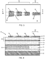
FIG. 3 is a top view of the structure at a fabrication stage subsequent to FIG. 1.
FIG. 4 is a cross-sectional view of the structure taken generally along line 4-4 in FIG. 3.
FIG. 5 is a cross-sectional view of the structure at a fabrication stage subsequent to FIG. 4.
FIG. 6 is a top view of a structure in accordance with alternative embodiments of the invention.
FIG. 7 is a cross-sectional view of the structure taken generally along line 7-7 in FIG. 6.
FIG. 7A is a cross-sectional view of the structure taken generally along line 7A-7A in FIG. 6.
FIG. 8 is a cross-sectional view of a structure in accordance with alternative embodiments of the invention.
FIG. 9 is a cross-sectional view of the structure taken generally along line 9-9 in FIG. 8.
FIG. 10 is a cross-sectional view of a structure in accordance with alternative embodiments of the invention.
FIG. 11 is a top view of a structure in accordance with alternative embodiments of the invention.
FIG. 12 is a cross-sectional view of the structure taken generally along line 12-12 in FIG. 11.
FIG. 12A is a cross-sectional view of the structure taken generally along line 12A-12A in FIG. 11.
DETAILED DESCRIPTION
With reference to FIGS. 1, 2 and in accordance with embodiments of the invention, a structure 10 for a multilayer coupler includes a waveguide core 12 having a tapered section 14 of a given length that terminates at an end surface 16. The tapered section 14 of the waveguide core 12 may extend lengthwise along a longitudinal axis 18. The tapered section 14 gradually becomes narrower in a direction along the longitudinal axis 18 with decreasing distance from the end surface 16. The tapered section 14 of the waveguide core 12 has a width dimension that varies with position along the longitudinal axis 18 and that has a minimum width occurring at the end surface 16. In an embodiment, the width dimension of the tapered section 14 may be narrowest at the end surface 16 and vary over its length based on a linear function to provide a trapezoidal shape. In an alternative embodiment, the width dimension of the tapered section 14 may be narrowest at the end surface 16 and vary over its length based on a non-linear function, such as a quadratic, parabolic, or exponential function.
The waveguide core 12 may be comprised of a single-crystal semiconductor material, such as single-crystal silicon. In an embodiment, the single-crystal semiconductor material may originate from a device layer of a silicon-on-insulator (SOI) substrate that further includes a dielectric layer 20 provided by a buried oxide layer and a substrate 22 comprised of a single-crystal semiconductor material, such as single-crystal silicon. The waveguide core 12 may be patterned from the device layer by lithography and etching processes during front-end-of-line processing. The waveguide core 12 and its tapered section 14 are positioned in a given layer or level over the dielectric layer 20 and the substrate 22.
With reference to FIGS. 3, 4 in which like reference numerals refer to like features in FIGS. 1, 2 and at a subsequent fabrication stage, a dielectric layer 24, a patterned dielectric layer 26, and dielectric layers 25, 27, 29, 31 are formed over the waveguide core 12 and dielectric layer 20. The dielectric layers 25, 29, 31 may be comprised of silicon dioxide, and the dielectric layer 27 may be comprised of silicon nitride. The silicon dioxide comprising the dielectric layers 25, 29, 31 may be formed by plasma-enhanced chemical vapor deposition using ozone and tetraethylorthosilicate (TEOS) as reactants. Alternatively, the silicon dioxide comprising one or more of the dielectric layers 25, 29, 31 may be fluorinated by adding fluorine as an additional reactant during plasma-enhanced chemical vapor deposition. Alternatively, the silicon dioxide comprising the dielectric layers 25, 29, 31 may comprise stacked sublayers containing tetraethylorthosilicate silicon dioxide and fluorinated-tetraethylorthosilicate silicon dioxide.
The dielectric layer 24 and the dielectric layers 25, 27, 29, 31 may be solid and non-patterned (i.e., unbroken) above the waveguide core 12. The dielectric layer 24, the dielectric layers 25, 27, 29, 31, and the patterned dielectric layer 26 may have a refractive index that is less than the refractive index of the waveguide core 12. The dielectric layer 24 and patterned dielectric layer 26 may have a refractive index that is greater than the refractive index of dielectric layers 25, 29, 31. The dielectric layer 27 may also have a refractive index that is greater than the refractive index of dielectric layers 25, 29, 31. The dielectric layer 27 is positioned in a vertical direction between the dielectric layers 25, 29, the dielectric layer 24 is positioned in a vertical direction between the dielectric layers 29, 31, and the dielectric layer 31 is positioned in a vertical direction between the dielectric layer 24 and the patterned dielectric layer 26. The dielectric layer 24 is positioned in a vertical direction between the waveguide core 12 and the patterned dielectric layer 26.
The dielectric layer 24 and the patterned dielectric layer 26 are comprised of a material having a different composition than the materials of the dielectric layers 25, 27, 29, 31. In an embodiment, the dielectric layer 24 and the patterned dielectric layer 26 may be comprised of silicon-carbon nitride (e.g., nitrogen-doped silicon carbide (SiCN)) deposited by chemical vapor deposition or plasma-enhanced chemical vapor deposition using reactants that supply silicon, carbon, and nitrogen. In an embodiment, the dielectric layer 24 and the patterned dielectric layer 26 may be comprised of hydrogenated silicon-carbon nitride (e.g., nitrogen-doped hydrogenated silicon carbide (SiCNH)) deposited by chemical vapor deposition or plasma-enhanced chemical vapor deposition using reactants that supply silicon, carbon, nitrogen, and hydrogen.
The dielectric layers 25, 27, 29, which may be formed by middle-of-line processing, may include contacts that are coupled to electronic components, such as field-effect transistors, and active optical components, such as a Mach-Zehnder modulator. The dielectric layer 24, the patterned dielectric layer 26, and the intervening dielectric layer 31 may be formed by back-end-of-line processing as levels in a back-end-of-line stack 48.
The patterned dielectric layer 26 includes a waveguide core 28 having a tapered section 30 and a grating coupler 32 with tapered segments 34 that provide the grating structures of the grating coupler 32. The tapered section 30 of the waveguide core 28 is positioned adjacent to the tapered segments 34 of the grating coupler 32, and the tapered section 30 and tapered segments 34 are arranged lengthwise along a longitudinal axis 38.
Each tapered segment 34 may gradually become narrower in a direction along the longitudinal axis 38 with increasing distance from an end surface 35 of the segment 34 furthest from the tapered section 30 of the waveguide core 28. In the representative embodiment, each tapered segment 34 is a ridge or strip that has a width dimension that decreases with decreasing distance from the tapered section 30 of the waveguide core 28. In an embodiment, the width dimension of the tapered segments 34 may be narrowest at the end surface 35 and vary over the length of the grating coupler based on a linear function. In the representative embodiment, the width dimensions of the tapered segments 34 are selected such that the grating coupler 32 is inversely tapered. In an embodiment, the tapered segments 34 and the tapered section 30 each define an inverse taper that is tapered in the opposite direction with respect to the tapering of the tapered section 14 of the waveguide core 12. As used herein, an inverse taper is a tapered section of waveguide core with a gradual increase in width along the propagation direction of the light guided by the inverse taper. In an embodiment, the width dimension of the tapered segments 34 may vary based on a linear function to provide a trapezoidal shape. In an alternative embodiment, the width dimension of the tapered segments 34 may vary based on a non-linear function, such as a quadratic, parabolic, or exponential function.
The patterned dielectric layer 26 may be formed by lithography and etching processes. The patterned dielectric layer 26 may be fully etched or, alternatively, only partially etched to define a thin slab layer coupled to a lower portion of the tapered segments 34 and at least the tapered section 30 of the waveguide core 28. The tapered segments 34 have an alternating arrangement with grooves 36 that separate adjacent pairs of the tapered segments 34 and that separate the tapered segment 34 at one end of the grating coupler 32 from the tapered section 30 of the waveguide core 28. If the patterned dielectric layer 26 is fully etched, the grooves 36 may extend to the dielectric layer 31 such that strips of the dielectric layer 31 are revealed between the tapered segments 34. In an embodiment, the pitch and duty cycle of the tapered segments 34 may be uniform to define a periodic arrangement. In alternative embodiments, the pitch and/or the duty cycle of the tapered segments 34 may be apodized (i.e., non-uniform) to define a non-periodic arrangement. The duty cycle and pitch of the tapered segments 34, as well as the dimensions of the tapered segments 34, may be selected to optimize phase matching with the tapered section 14 of the waveguide core 12.
The waveguide core 28 and the grating coupler 32 are positioned in a given layer or level in the back-end-of-line stack 48 over the dielectric layer 20 on the substrate 22. The level of the waveguide core 28 and the grating coupler 32 differs in elevation above the dielectric layer 20 from the level of the waveguide core 12 and its tapered section 14. The dielectric layer 24 is also positioned in a given layer or level in the back-end-of-line stack 48 over the dielectric layer 20 on the substrate 22, and the level of the dielectric layer 24 differs in elevation above the dielectric layer 20 from the level of the waveguide core 28 and grating coupler 32 and differs in elevation above the dielectric layer 20 from the level of the waveguide core 12 and its tapered section 14.
The tapered segments 34 of the grating coupler 32 are positioned over the tapered section 14 of the waveguide core 12 and have an overlapping relationship with the tapered section 14 of the waveguide core 12. In an embodiment, the tapered segments 34 of the grating coupler 32 may be centered over the tapered section 14 of the waveguide core 12. In an embodiment, the tapered segments 34 of the grating coupler 32 may be wider than the tapered section 14 of the waveguide core 12 at any position along the longitudinal axes 18, 38. In an embodiment, the longitudinal axis 18 may be aligned parallel to the longitudinal axis 38. The overlapped positioning may promote the efficient interlayer transmission of optical signals from the waveguide core 12 upward to the waveguide core 28.
In the representative embodiment, the dielectric layer 24 is positioned between the grating coupler 32 and the waveguide core 12 such that a single solid and non-patterned layer comprised of the same material as the waveguide core 28 and the grating coupler 32 is positioned in a vertical direction between the tapered section 14 of the waveguide core 12 and the grating coupler 32. In an alternative embodiment, the dielectric layer 24 may be patterned to form the waveguide core 28 and the grating coupler 32, and the dielectric layer 26 may be solid and non-patterned such that a solid and non-patterned layer comprised of the same material as the waveguide core 28 and the grating coupler 32 is not positioned in a vertical direction between the tapered section 14 of the waveguide core 12 and the grating coupler 32.
With reference to FIG. 5 in which like reference numerals refer to like features in FIG. 4 and at a subsequent fabrication stage, additional dielectric layers 39, 40, 41, 42, 43, 44, 45 of the back-end-of-line stack 48 are formed by back-end-of-line processing over the patterned dielectric layer 26 and the dielectric layer 31. The dielectric layers 39, 41, 44 may be comprised of silicon dioxide (e.g., tetraethylorthosilicate silicon dioxide and/or fluorinated-tetraethylorthosilicate silicon dioxide), the dielectric layers 43, 45 may be comprised of silicon nitride, and the dielectric layers 40, 42 may be comprised of either silicon-carbon nitride or hydrogenated silicon-carbon nitride. Portions of the dielectric layer 39 may fill the grooves 36 between the tapered segments 34 of the grating coupler 32.
The dielectric layer 40 is arranged in a vertical direction between the dielectric layers 39, 41, the dielectric layer 42 is arranged in a vertical direction between the dielectric layers 41, 43, and the dielectric layer 44 is arranged in a vertical direction between the dielectric layers 43, 45. The dielectric layer 43 may directly contact the dielectric layer 42. The dielectric layers 40, 42 are positioned in given layers or levels over the dielectric layer 20 on the substrate 22, and the levels of the dielectric layers 40, 42 differ in elevation above the dielectric layer 20 from the level of the grating coupler 32 and also differ in elevation above the dielectric layer 20 from the level of the waveguide core 12 and its tapered section 14.
In an alternative embodiment, the dielectric layer 40 may be patterned to form the waveguide core 28 and the grating coupler 32, and the dielectric layers 24, 26 may be solid and non-patterned. In this embodiments, multiple dielectric layers 24, 26 that are solid and non-patterned, and that are comprised of the same material as the waveguide core 28 and the grating coupler 32, may be positioned in a vertical direction between the tapered section 14 of the waveguide core 12 and the grating coupler 32.
In use, optical signals are guided by the waveguide core 12 to the structure 10. The arriving optical signals are transmitted upwardly from the tapered section 14 of the waveguide core 12 to the grating coupler 32 located in the back-end-of-line stack 48. The waveguide core 28, which is also located in the back-end-of-line stack 48, guides the optical signals away from the grating coupler 32.
The structure 10 includes layers of different materials arranged in different levels of a multiple-level coupler. The structure 10, in any of its embodiments described herein, may be integrated into a photonics chip that may include electronic components and additional optical components in addition to the structure 10. The electronic components may include, for example, field-effect transistors that are fabricated by CMOS processing using the device layer of the silicon-on-insulator substrate. The back-end-of-line stack 48 may include metal lines that are stacked into the different levels and that are vertically interconnected through vias with the electronic components and active optical components. The metal lines of the back-end-of-line stack 48 may be absent in the vicinity of the structure 10 so as to not interfere with the multilevel transfer of optical signals by the structure 10.
With reference to FIGS. 6, 7, 7A and in accordance with alternative embodiments of the invention, the structure 10 may be modified to introduce a grating coupler 50 that is optically coupled to the waveguide core 12, to provide the waveguide core 28 with a tapered section 54 that is not segmented, and to eliminate the grating coupler 32 from the patterned dielectric layer 26. The grating coupler 50 includes segments 52 that supply grating structures. The segments 52 have an alternating arrangement with grooves that separate adjacent pairs of segments 52. In an embodiment, the pitch and duty cycle of the segments 52 may be uniform to define a periodic arrangement. In alternative embodiments, the pitch and/or the duty cycle of the segments 52 may be apodized (i.e., non-uniform) to define a non-periodic arrangement.
The segments 52 of the grating coupler 50 may be comprised of, for example, polycrystalline silicon (i.e., polysilicon). The segments 52 of the grating coupler 50 may be formed, for example, by depositing a layer of polysilicon and patterning the deposited polysilicon layer with lithography and etching processes. The dielectric layer 27 may conformally extend across the segments 52 and portions of the waveguide core 12 not covered by the segments 52. The waveguide core 12 may be a straight waveguide core that is non-tapered. The segments 52 may be surrounded by a layer (not shown) comprised of a material (e.g., silicon dioxide) having a different composition than the material of the dielectric layer 27.
The waveguide core 28 and its tapered section 54 are positioned in a given layer or level over the dielectric layer 20 on the substrate 22. The level of the tapered section 54 differs in elevation above the dielectric layer 20 from the level of the grating coupler 50. The tapered section 54 of the waveguide core 28 is positioned over the segments 52 of the grating coupler 50 and overlaps with the segments 52 of the grating coupler 50. In particular, the tapered section 54 is terminated by an end surface 56 that is located over the segments 52 of the grating coupler 50. In an embodiment, the tapered section 54 of the waveguide core 28 may be centered over the segments 52 of the grating coupler 50. The overlapped positioning of the tapered section 54 over the grating coupler 50 may promote the efficient transfer of optical signals from the waveguide core 12 upward to the waveguide core 28. In an embodiment, the segments 52 and the waveguide core 12 may have substantially equal width dimensions, and the width dimension of the tapered section 54 may be greater than the width dimension of the segments 52 where overlapped.
Processing of the structure 10 continues as described in connection with FIG. 5.
With reference to FIGS. 8, 9 and in accordance with alternative embodiments of the invention, the dielectric layers 42, 43 may be patterned to form a waveguide core 68 similar to the waveguide core 28 and a grating coupler 72 similar to the grating coupler 32, and the dielectric layers 24, 26, 40 may be solid and non-patterned. The dielectric layers 24, 26, 40, which are solid and non-patterned, are comprised of the same dielectric material as lower portions of the waveguide core 68 and the grating coupler 72, and the dielectric layers 24, 26, 40 are positioned in a vertical direction between the tapered section 14 of the waveguide core 12 and the grating coupler 72. The grating coupler 72 includes tapered segments 64 similar to tapered segments 34, grooves 66 similar to grooves 36 between adjacent tapered segments 64, and a tapered section 70 similar to tapered section 30. The tapered segments 64 of the grating coupler 72 are comprised of multiple dielectric materials, in this instance the material of the dielectric layer 42 as a lower portion and the material of the dielectric layer 43 as an upper portion. The tapered segments 64 and the tapered section 70 are positioned along a longitudinal axis 78. In an embodiment, the tapered segments 64 of the grating coupler 72 may be centered over the tapered segments 34 of the grating coupler 32 and the tapered section 14 of the waveguide core 12.
Processing of the structure 10 continues as described in connection with FIG. 5 to form the dielectric layers 44, 45 over the waveguide core 68 and grating coupler 72.
With reference to FIG. 10 and in accordance with alternative embodiments of the invention, the structure 10 may include a waveguide core 82 and a grating coupler 84 that replace the waveguide core 12, and both of the grating couplers 32, 72. Optical signals from the grating coupler 84 to both of the grating couplers 32, 72 and distributed to the waveguide cores 28, 68 within multiple levels in the back-end-of-line stack 48. The grating coupler 84 may include tapered segments 86 similar to tapered segments 34 and grooves similar to grooves 36 between adjacent tapered segments 86. In an embodiment, the tapered segments 64 of the grating coupler 72 may be centered over the tapered segments 34 of the grating coupler 32.
The waveguide core 82 and grating coupler 84 may be formed by depositing a layer of a material (e.g., silicon nitride) on the dielectric layer 25 and patterning the deposited layer by lithography and etching processes during middle-of-line processing. In an alternative embodiment, the waveguide core 82 and grating coupler 84 may be comprised of a different material, such as single-crystal silicon, that is formed by processing similar to that described in connection with the formation of the waveguide core 12.
With reference to FIGS. 11, 12, 12A and in accordance with alternative embodiments of the invention, the structure 10 may include a grating coupler 94 that is positioned over the tapered section 54. The grating coupler 94 includes segments 96 and grooves 95 that are positioned between adjacent segments 96. In an embodiment, the segments 96 of the grating coupler 94 may be wider than the tapered section 54 where overlapped. The grating coupler 94 may be formed by patterning the dielectric layer 40 by lithography and etching processes. The grating coupler 94 may function as a reflector to reflect optical signals that are not captured by the tapered section 54 of the waveguide core 28 downwardly toward the tapered section 54, which may provide for improved light confinement and reduced light leakage.
Processing of the structure 10 continues as described in connection with FIG. 5 to form dielectric layers 41, 42 43, 44, 45.
The methods as described above are used in the fabrication of integrated circuit chips. The resulting integrated circuit chips can be distributed by the fabricator in raw wafer form (e.g., as a single wafer that has multiple unpackaged chips), as a bare die, or in a packaged form. The chip may be integrated with other chips, discrete circuit elements, and/or other signal processing devices as part of either an intermediate product or an end product. The end product can be any product that includes integrated circuit chips, such as computer products having a central processor or smartphones.
References herein to terms modified by language of approximation, such as “about”, “approximately”, and “substantially”, are not to be limited to the precise value specified. The language of approximation may correspond to the precision of an instrument used to measure the value and, unless otherwise dependent on the precision of the instrument, may indicate +/−10% of the stated value(s).
References herein to terms such as “vertical”, “horizontal”, etc. are made by way of example, and not by way of limitation, to establish a frame of reference. The term “horizontal” as used herein is defined as a plane parallel to a conventional plane of a semiconductor substrate, regardless of its actual three-dimensional spatial orientation. The terms “vertical” and “normal” refer to a direction perpendicular to the horizontal, as just defined. The term “lateral” refers to a direction within the horizontal plane.
A feature “connected” or “coupled” to or with another feature may be directly connected or coupled to or with the other feature or, instead, one or more intervening features may be present. A feature may be “directly connected” or “directly coupled” to or with another feature if intervening features are absent. A feature may be “indirectly connected” or “indirectly coupled” to or with another feature if at least one intervening feature is present. A feature “on” or “contacting” another feature may be directly on or in direct contact with the other feature or, instead, one or more intervening features may be present. A feature may be “directly on” or in “direct contact” with another feature if intervening features are absent. A feature may be “indirectly on” or in “indirect contact” with another feature if at least one intervening feature is present. Different features overlap if a feature extends over, and covers a part of, another feature.
The descriptions of the various embodiments of the present invention have been presented for purposes of illustration but are not intended to be exhaustive or limited to the embodiments disclosed. Many modifications and variations will be apparent to those of ordinary skill in the art without departing from the scope and spirit of the described embodiments. The terminology used herein was chosen to best explain the principles of the embodiments, the practical application or technical improvement over technologies found in the marketplace, or to enable others of ordinary skill in the art to understand the embodiments disclosed herein.

Claims (20)

What is claimed is:
1. A structure comprising:
a substrate;
a dielectric layer on the substrate;
a first waveguide core including a tapered section, the first waveguide core positioned in a first level over the dielectric layer;
a second waveguide core positioned in a second level over the dielectric layer, the second level differing in elevation above the dielectric layer from the first level; and
a first grating coupler including a plurality of segments positioned in the second level adjacent to the second waveguide core,
wherein the segments of the first grating coupler and the tapered section of the first waveguide core are positioned in a first overlapping arrangement.
2. The structure of claim 1 wherein the second waveguide core and the segments of the first grating coupler comprise nitrogen-doped silicon carbide or nitrogen-doped hydrogenated silicon carbide.
3. The structure of claim 2 further comprising:
a back-end-of-line stack over the dielectric layer,
wherein the back-end-of-line stack includes the second waveguide core and the first grating coupler, and the segments of the first grating coupler are positioned over the tapered section of the first waveguide core.
4. The structure of claim 3 wherein each segment of the first grating coupler includes a first layer comprised of nitrogen-doped silicon carbide or nitrogen-doped hydrogenated silicon carbide and a second layer comprised of silicon nitride.
5. The structure of claim 3 wherein the segments of the first grating coupler are centered over the tapered section of the first waveguide core.
6. The structure of claim 2 wherein the tapered section is tapered in a first direction, and the segments of the first grating coupler are inversely tapered in a second direction opposite to the first direction.
7. The structure of claim 1 wherein the first waveguide core comprises nitrogen-doped silicon carbide or nitrogen-doped hydrogenated silicon carbide.
8. The structure of claim 7 further comprising:
a back-end-of-line stack over the dielectric layer,
wherein the back-end-of-line stack includes the first waveguide core, and the tapered section of the first waveguide core is positioned over the segments of the first grating coupler.
9. The structure of claim 8 wherein the back-end-of-line stack includes a second grating coupler having a plurality of segments comprised of nitrogen-doped silicon carbide or nitrogen-doped hydrogenated silicon carbide, the second grating coupler is positioned in a third level over the dielectric layer, the third level differs in elevation above the dielectric layer from the first level and the second level, and the segments of the second grating coupler are positioned over the tapered section of the first waveguide core in a second overlapping arrangement.
10. The structure of claim 9 wherein the tapered section of the first waveguide core is positioned in a vertical direction between the segments of the first grating coupler and the segments of the second grating coupler.
11. The structure of claim 7 wherein the tapered section of the first waveguide core is centered over the segments of the first grating coupler.
12. A structure comprising:
a substrate;
a dielectric layer on the substrate;
a first waveguide core positioned in a first level over the dielectric layer;
a first grating coupler positioned in the first level adjacent to the first waveguide core;
a second waveguide core positioned in a second level over the dielectric layer; and
a second grating coupler including a plurality of segments positioned in the second level adjacent to the second waveguide core,
wherein the segments of the second grating coupler and the segments of the first grating coupler are positioned in an overlapping arrangement.
13. The structure of claim 12 wherein the first grating coupler, the first waveguide core, the second waveguide core, and the second grating coupler comprise nitrogen-doped silicon carbide or nitrogen-doped hydrogenated silicon carbide.
14. The structure of claim 13 further comprising:
a back-end-of-line stack over the dielectric layer,
wherein the back-end-of-line stack includes the first waveguide core, the first grating coupler, the second waveguide core, and the second grating coupler, and the segments of the second grating coupler are positioned over the segments of the first grating coupler.
15. The structure of claim 14 wherein each segment of the second grating coupler includes a first layer comprised of nitrogen-doped silicon carbide or nitrogen-doped hydrogenated silicon carbide and a second layer comprised of silicon nitride.
16. A method comprising:
forming a first waveguide core positioned within a first level over a dielectric layer on a substrate, wherein the first waveguide core includes a tapered section; and
forming a second waveguide core and a grating coupler adjacent to the second waveguide core, wherein the second waveguide core and the grating coupler are positioned in a second level over the dielectric layer, the second level differs in elevation above the dielectric layer from the first level, and the grating coupler includes a plurality of segments positioned in an overlapping arrangement with the tapered section of the first waveguide core.
17. The method of claim 16 wherein the second waveguide core and the segments of the grating coupler comprise nitrogen-doped silicon carbide or nitrogen-doped hydrogenated silicon carbide.
18. The method of claim 17 further comprising:
forming a back-end-of-line stack over the dielectric layer,
wherein the back-end-of-line stack includes the second waveguide core and the grating coupler, and the segments of the grating coupler are positioned over the tapered section of the first waveguide core.
19. The method of claim 16 wherein the first waveguide core comprises nitrogen-doped silicon carbide or nitrogen-doped hydrogenated silicon carbide.
20. The method of claim 19 further comprising:
forming a back-end-of-line stack over the dielectric layer,
wherein the back-end-of-line stack includes the first waveguide core, and the tapered section of the first waveguide core is positioned over the segments of the grating coupler.
US17/146,864 2021-01-12 2021-01-12 Optical components in the back-end-of-line stack of a photonics chip using plural cores vertically stacked Active US11378743B1 (en)

Priority Applications (3)

Application Number Priority Date Filing Date Title
US17/146,864 US11378743B1 (en) 2021-01-12 2021-01-12 Optical components in the back-end-of-line stack of a photonics chip using plural cores vertically stacked
DE102021132105.0A DE102021132105A1 (en) 2021-01-12 2021-12-07 OPTICAL COMPONENTS IN THE BACK-END OF-LINE STACK OF A PHOTONIC CHIP
CN202111505812.8A CN114764164A (en) 2021-01-12 2021-12-10 Optical assembly in back end of line stack of photonic chips

Applications Claiming Priority (1)

Application Number Priority Date Filing Date Title
US17/146,864 US11378743B1 (en) 2021-01-12 2021-01-12 Optical components in the back-end-of-line stack of a photonics chip using plural cores vertically stacked

Publications (2)

Publication Number Publication Date
US11378743B1 true US11378743B1 (en) 2022-07-05
US20220221650A1 US20220221650A1 (en) 2022-07-14

Family

ID=82116481

Family Applications (1)

Application Number Title Priority Date Filing Date
US17/146,864 Active US11378743B1 (en) 2021-01-12 2021-01-12 Optical components in the back-end-of-line stack of a photonics chip using plural cores vertically stacked

Country Status (3)

Country Link
US (1) US11378743B1 (en)
CN (1) CN114764164A (en)
DE (1) DE102021132105A1 (en)

Cited By (8)

* Cited by examiner, † Cited by third party
Publication number Priority date Publication date Assignee Title
US11567260B1 (en) * 2021-10-14 2023-01-31 Globalfoundries U.S. Inc. Photonics chips with ambient light shadowing of optical components
US20240012200A1 (en) * 2022-07-11 2024-01-11 Globalfoundries U.S. Inc. Gratings with non-rectangular segments
US20240045159A1 (en) * 2022-08-03 2024-02-08 Taiwan Semiconductor Manufacturing Company Ltd. Photonic structure and method for manufacturing the same
US11934008B2 (en) 2021-02-11 2024-03-19 Globalfoundries U.S. Inc. Metamaterial edge couplers in the back-end-of-line stack of a photonics chip
US11947168B2 (en) 2022-04-05 2024-04-02 Globalfoundries U.S. Inc. Stacked edge couplers in the back-end-of-line stack of a photonic chip
US20240184042A1 (en) * 2022-12-01 2024-06-06 Globalfoundries U.S. Inc. Optical components with one or more embedded bragg reflectors
US20240288631A1 (en) * 2023-02-28 2024-08-29 Globalfoundries U.S. Inc. Waveguide escalators for a photonics chip
US12498524B2 (en) 2023-06-14 2025-12-16 Globalfoundries U.S. Inc. Structures including a grating coupler and a layer exhibiting an electric-field-induced pockels effect

Families Citing this family (3)

* Cited by examiner, † Cited by third party
Publication number Priority date Publication date Assignee Title
EP4102272B1 (en) * 2021-06-08 2025-02-19 IHP GmbH - Innovations for High Performance Microelectronics / Leibniz-Institut für innovative Mikroelektronik Integrated optoelectronic device with optical interconnect structure for improved beol device integration
CN117130095B (en) * 2023-08-31 2024-06-25 Nano科技(北京)有限公司 Chip stacking and packaging system and optical connection method of multi-layer chips
WO2025134093A1 (en) * 2023-12-21 2025-06-26 Lionix International Bv Waveguide-grating coupler comprising a vertically tapered region

Citations (15)

* Cited by examiner, † Cited by third party
Publication number Priority date Publication date Assignee Title
US5033812A (en) * 1989-02-17 1991-07-23 Sharp Kabushiki Kaisha Grating coupler
US20030231375A1 (en) * 2002-06-14 2003-12-18 Jung-Jin Ju Wavelength converter, method of manufacturing wavelength converter and optical device using the same
US20040126072A1 (en) * 2001-08-02 2004-07-01 Hoon Lee Howard Wing Optical devices with engineered nonlinear nanocomposite materials
US20040156589A1 (en) * 2003-02-11 2004-08-12 Luxtera, Inc Optical waveguide grating coupler incorporating reflective optical elements and anti-reflection elements
US6944192B2 (en) * 2001-03-14 2005-09-13 Corning Incorporated Planar laser
US7005669B1 (en) * 2001-08-02 2006-02-28 Ultradots, Inc. Quantum dots, nanocomposite materials with quantum dots, devices with quantum dots, and related fabrication methods
US20080043242A1 (en) * 2004-07-15 2008-02-21 Emmerson Gregory D Optical Sensors
US20080193079A1 (en) * 2007-02-13 2008-08-14 National Research Council Of Canada Interface Device For Performing Mode Transformation in Optical Waveguides
US20080193080A1 (en) * 2007-02-13 2008-08-14 National Research Council Of Canada Interface device for performing mode transformation in optical waveguides
US20110150018A1 (en) * 2009-12-17 2011-06-23 Electronics And Telecommunications Research Institute Laser device
US20150338286A1 (en) * 2012-03-07 2015-11-26 Ofs Fitel, Llc Grating-based sensor
US20180011249A1 (en) * 2016-07-11 2018-01-11 University Of Maryland Fiber-to-waveguide couplers with ultra high coupling efficiency and integrated chip waveguides including the same
US20200081155A1 (en) * 2018-04-28 2020-03-12 38th Research Institute Of China Electronics Technology Group Corp. Chip with beamforming network based on photonic crystal resonant cavity tree structure and fabrication method thereof
US10746907B2 (en) 2018-04-04 2020-08-18 Globalfoundries Inc. Grating couplers with cladding layer(s)
US10816726B1 (en) * 2019-08-23 2020-10-27 Globalfoundries Inc. Edge couplers for photonics applications

Family Cites Families (12)

* Cited by examiner, † Cited by third party
Publication number Priority date Publication date Assignee Title
KR100803288B1 (en) * 2006-12-20 2008-02-13 인하대학교 산학협력단 Polymer Condensing Waveguide Grating Coupler and Optical PCC
WO2015111458A1 (en) * 2014-01-24 2015-07-30 技術研究組合光電子融合基盤技術研究所 Grating coupler
WO2015139200A1 (en) * 2014-03-18 2015-09-24 华为技术有限公司 Grating coupler and manufacturing method therefor
CN107290824B (en) * 2016-04-13 2020-01-10 华为技术有限公司 Waveguide structure and preparation method
US9715064B1 (en) * 2016-09-13 2017-07-25 Globalfoundries Inc. Multi-chip modules with vertically aligned grating couplers for transmission of light signals between optical waveguides
US10126500B2 (en) * 2016-11-01 2018-11-13 Purdue Research Foundation Optical coupler having exposed subwavelength gratings for coupling electromagnetic field
EP4387016A3 (en) * 2016-12-06 2025-01-08 Finisar Corporation Surface coupled laser with optical interposer
US10429582B1 (en) * 2018-05-02 2019-10-01 Globalfoundries Inc. Waveguide-to-waveguide couplers with multiple tapers
US10185092B1 (en) * 2018-07-11 2019-01-22 Globalfoundries Inc. Hybrid grating couplers that overlap via an interconnect structure having a metallization layer
CN109031522A (en) * 2018-07-16 2018-12-18 浙江工业大学 A kind of grating coupler of low back-reflection
CN111638575B (en) * 2020-07-03 2022-09-23 中国电子科技集团公司第三十八研究所 An Optical Delay Array Chip Based on Chirped Bragg Gratings
CN111965761B (en) * 2020-08-18 2022-08-19 上海交通大学 Grating coupler based on lithium niobate thin film material and manufacturing method thereof

Patent Citations (27)

* Cited by examiner, † Cited by third party
Publication number Priority date Publication date Assignee Title
US5033812B1 (en) * 1989-02-17 1993-10-12 Sharp Kabushiki Kaisha Grating coupler with a tapering waveguide for changing a coupling coefficient
US5033812A (en) * 1989-02-17 1991-07-23 Sharp Kabushiki Kaisha Grating coupler
US6944192B2 (en) * 2001-03-14 2005-09-13 Corning Incorporated Planar laser
US7020372B2 (en) * 2001-08-02 2006-03-28 Ultradots, Inc. Optical devices with engineered nonlinear nanocomposite materials
US6819845B2 (en) * 2001-08-02 2004-11-16 Ultradots, Inc. Optical devices with engineered nonlinear nanocomposite materials
US20050058415A1 (en) * 2001-08-02 2005-03-17 Lee Howard Wing Hoon Optical devices with engineered nonlinear nanocomposite materials
US20050058416A1 (en) * 2001-08-02 2005-03-17 Hoon Lee Howard Wing Optical devices with engineered nonlinear nanocomposite materials
US20040126072A1 (en) * 2001-08-02 2004-07-01 Hoon Lee Howard Wing Optical devices with engineered nonlinear nanocomposite materials
US6961499B2 (en) * 2001-08-02 2005-11-01 Ultradots, Inc. Optical devices with engineered nonlinear nanocomposite materials
US7005669B1 (en) * 2001-08-02 2006-02-28 Ultradots, Inc. Quantum dots, nanocomposite materials with quantum dots, devices with quantum dots, and related fabrication methods
US6927895B2 (en) * 2002-06-14 2005-08-09 Electronics And Telecommunications Research Institute Wavelength converter, method of manufacturing wavelength converter and optical device using the same
US20030231375A1 (en) * 2002-06-14 2003-12-18 Jung-Jin Ju Wavelength converter, method of manufacturing wavelength converter and optical device using the same
US20040156589A1 (en) * 2003-02-11 2004-08-12 Luxtera, Inc Optical waveguide grating coupler incorporating reflective optical elements and anti-reflection elements
US7541573B2 (en) * 2004-07-15 2009-06-02 University Of Southampton Optical sensors for sensing the refractive index of fluid samples
US20080043242A1 (en) * 2004-07-15 2008-02-21 Emmerson Gregory D Optical Sensors
US20080193079A1 (en) * 2007-02-13 2008-08-14 National Research Council Of Canada Interface Device For Performing Mode Transformation in Optical Waveguides
US20080193080A1 (en) * 2007-02-13 2008-08-14 National Research Council Of Canada Interface device for performing mode transformation in optical waveguides
US7680371B2 (en) * 2007-02-13 2010-03-16 National Research Council Of Canada Interface device for performing mode transformation in optical waveguides
US20110150018A1 (en) * 2009-12-17 2011-06-23 Electronics And Telecommunications Research Institute Laser device
US8213478B2 (en) * 2009-12-17 2012-07-03 Electronics And Telecommunications Research Institute Laser device
US20150338286A1 (en) * 2012-03-07 2015-11-26 Ofs Fitel, Llc Grating-based sensor
US9574950B2 (en) * 2012-03-07 2017-02-21 Ofs Fitel, Llc Grating-based sensor
US20180011249A1 (en) * 2016-07-11 2018-01-11 University Of Maryland Fiber-to-waveguide couplers with ultra high coupling efficiency and integrated chip waveguides including the same
US10746907B2 (en) 2018-04-04 2020-08-18 Globalfoundries Inc. Grating couplers with cladding layer(s)
US20200081155A1 (en) * 2018-04-28 2020-03-12 38th Research Institute Of China Electronics Technology Group Corp. Chip with beamforming network based on photonic crystal resonant cavity tree structure and fabrication method thereof
US10816696B2 (en) * 2018-04-28 2020-10-27 38th Research Institute Of China Electronics Technology Group Corp. Chip with beamforming network based on photonic crystal resonant cavity tree structure and fabrication method thereof
US10816726B1 (en) * 2019-08-23 2020-10-27 Globalfoundries Inc. Edge couplers for photonics applications

Non-Patent Citations (5)

* Cited by examiner, † Cited by third party
Title
J. Yao et al., "Grating-coupler based low-loss optical interlayer coupling," 8th IEEE International Conference on Group IV Photonics, London, 2011, pp. 383-385, doi: 10.1109/GROUP4.2011.6053824.
K. Giewont et al., "300-mm Monolithic Silicon Photonics Foundry Technology," in IEEE Journal of Selected Topics in Quantum Electronics, vol. 25, No. 5, pp. 1-11, Sep.-Oct. 2019, Art No. 8200611, doi: 10.1109/JSTQE.2019.2908790.
M. Rakowski, C. Meagher, K. Nummy, A. Aboketaf, J. Ayala, Y. Bian, B. Harris, K. Mclean, K. McStay, A. Sahin, L. Medina, B. Peng, Z. Sowinski, A. Stricker, T. Houghton, C. Hedges, K. Giewont, A. Jacob, T. Letavic, D. Riggs, A. Yu, and J. Pellerin, "45nm CMOS—Silicon Photonics Monolithic Technology (45CLO) for next-generation, low power and high speed optical interconnects," in Optical Fiber Communication Conference (OFC) 2020, OSA Technical Digest (Optical Society of America, 2020), paper T3H.3.
Majid Sodagar, Reza Pourabolghasem, Ali A. Eftekhar, and Ali Adibi, "High-efficiency and wideband interlayer grating couplers in multilayer Si/SiO2/SiN platform for 3D integration of optical functionalities," Opt. Express 22, 16767-16777 (2014).
Y. Bian, et al., "Towards low-loss monolithic silicon and nitride photonic building blocks in state-of-the-art 300mm CMOS foundry," in Frontiers in Optics / Laser Science, B. Lee, C. Mazzali, K. Corwin, and R. Jason Jones, eds., OSA Technical Digest (Optical Society of America, 2020), paper FW5D.2.

Cited By (12)

* Cited by examiner, † Cited by third party
Publication number Priority date Publication date Assignee Title
US11934008B2 (en) 2021-02-11 2024-03-19 Globalfoundries U.S. Inc. Metamaterial edge couplers in the back-end-of-line stack of a photonics chip
US11567260B1 (en) * 2021-10-14 2023-01-31 Globalfoundries U.S. Inc. Photonics chips with ambient light shadowing of optical components
US11947168B2 (en) 2022-04-05 2024-04-02 Globalfoundries U.S. Inc. Stacked edge couplers in the back-end-of-line stack of a photonic chip
US20240012200A1 (en) * 2022-07-11 2024-01-11 Globalfoundries U.S. Inc. Gratings with non-rectangular segments
US12339495B2 (en) * 2022-07-11 2025-06-24 Globalfoundries U.S. Inc. Gratings with non-rectangular segments
US20240045159A1 (en) * 2022-08-03 2024-02-08 Taiwan Semiconductor Manufacturing Company Ltd. Photonic structure and method for manufacturing the same
US12474532B2 (en) * 2022-08-03 2025-11-18 Taiwan Semiconductor Manufacturing Company Ltd. Photonic structure and method for manufacturing the same
US20240184042A1 (en) * 2022-12-01 2024-06-06 Globalfoundries U.S. Inc. Optical components with one or more embedded bragg reflectors
US12276835B2 (en) * 2022-12-01 2025-04-15 Globalfoundries U.S. Inc. Optical components with one or more embedded Bragg reflectors and tapered waveguide cores
US20240288631A1 (en) * 2023-02-28 2024-08-29 Globalfoundries U.S. Inc. Waveguide escalators for a photonics chip
US12353004B2 (en) * 2023-02-28 2025-07-08 Globalfoundries U.S. Inc. Waveguide escalators for a photonics chip
US12498524B2 (en) 2023-06-14 2025-12-16 Globalfoundries U.S. Inc. Structures including a grating coupler and a layer exhibiting an electric-field-induced pockels effect

Also Published As

Publication number Publication date
CN114764164A (en) 2022-07-19
DE102021132105A1 (en) 2022-07-14
US20220221650A1 (en) 2022-07-14

Similar Documents

Publication Publication Date Title
US11378743B1 (en) Optical components in the back-end-of-line stack of a photonics chip using plural cores vertically stacked
US11662523B2 (en) Edge couplers in the back-end-of-line stack of a photonics chip
US11782214B2 (en) Optical fiber coupler having hybrid tapered waveguide segments and metamaterial segments
US10816726B1 (en) Edge couplers for photonics applications
US11934008B2 (en) Metamaterial edge couplers in the back-end-of-line stack of a photonics chip
US11467341B2 (en) Waveguide crossings including a segmented waveguide section
US10585245B1 (en) Multiple-layer arrangements using tunable materials to provide switchable optical components
US10795083B1 (en) Heterogeneous directional couplers for photonics chips
US11150407B2 (en) Optical couplers with non-linear tapering
US11513286B2 (en) Heterogenous optical power splitter/combiner
US11493686B2 (en) Optical components with power-handling assistance
US10816727B1 (en) Multimode waveguide bends with features to reduce bending loss
US11256030B1 (en) Optical power splitters including a non-linear waveguide taper
US11036003B2 (en) Waveguide couplers providing conversion between waveguides
US10718903B1 (en) Waveguide crossings with a non-contacting arrangement
CN114815055B (en) Bragg grating with silicide coating segments
US10816872B1 (en) Tunable grating couplers
US10895689B2 (en) Switchable and reconfigurable grating couplers
US11803010B2 (en) Optical couplers with diagonal light transfer
US11409040B1 (en) Optical couplers for ridge-to-rib waveguide core transitions
CN114488393B (en) Optical power splitter with multi-level arrangement
US11269142B2 (en) Optical couplers with segmented waveguides
US10989872B1 (en) Waveguide bends with mode confinement
EP4220257B1 (en) Multiple-core heterogeneous waveguide structures including multiple slots
US12248177B2 (en) Waveguide crossings with a multiple-level non-contacting arrangement

Legal Events

Date Code Title Description
AS Assignment

Owner name: GLOBALFOUNDRIES U.S. INC., CALIFORNIA

Free format text: ASSIGNMENT OF ASSIGNORS INTEREST;ASSIGNORS:BIAN, YUSHENG;AUGUR, RODERICK A.;GIEWONT, KENNETH J.;AND OTHERS;SIGNING DATES FROM 20210110 TO 20210111;REEL/FRAME:054893/0989

FEPP Fee payment procedure

Free format text: ENTITY STATUS SET TO UNDISCOUNTED (ORIGINAL EVENT CODE: BIG.); ENTITY STATUS OF PATENT OWNER: LARGE ENTITY

STCF Information on status: patent grant

Free format text: PATENTED CASE

MAFP Maintenance fee payment

Free format text: PAYMENT OF MAINTENANCE FEE, 4TH YEAR, LARGE ENTITY (ORIGINAL EVENT CODE: M1551); ENTITY STATUS OF PATENT OWNER: LARGE ENTITY

Year of fee payment: 4