US11375144B2 - Method and system for reducing thermal shading in image sensor using on chip localized heat source - Google Patents
Method and system for reducing thermal shading in image sensor using on chip localized heat source Download PDFInfo
- Publication number
- US11375144B2 US11375144B2 US16/994,294 US202016994294A US11375144B2 US 11375144 B2 US11375144 B2 US 11375144B2 US 202016994294 A US202016994294 A US 202016994294A US 11375144 B2 US11375144 B2 US 11375144B2
- Authority
- US
- United States
- Prior art keywords
- heating elements
- image sensor
- cmos image
- subset
- regions
- Prior art date
- Legal status (The legal status is an assumption and is not a legal conclusion. Google has not performed a legal analysis and makes no representation as to the accuracy of the status listed.)
- Active
Links
Images


Classifications
-
- H04N5/3745—
-
- H—ELECTRICITY
- H04—ELECTRIC COMMUNICATION TECHNIQUE
- H04N—PICTORIAL COMMUNICATION, e.g. TELEVISION
- H04N25/00—Circuitry of solid-state image sensors [SSIS]; Control thereof
- H04N25/70—SSIS architectures; Circuits associated therewith
- H04N25/76—Addressed sensors, e.g. MOS or CMOS sensors
- H04N25/77—Pixel circuitry, e.g. memories, A/D converters, pixel amplifiers, shared circuits or shared components
-
- H—ELECTRICITY
- H04—ELECTRIC COMMUNICATION TECHNIQUE
- H04N—PICTORIAL COMMUNICATION, e.g. TELEVISION
- H04N25/00—Circuitry of solid-state image sensors [SSIS]; Control thereof
- H04N25/60—Noise processing, e.g. detecting, correcting, reducing or removing noise
- H04N25/61—Noise processing, e.g. detecting, correcting, reducing or removing noise the noise originating only from the lens unit, e.g. flare, shading, vignetting or "cos4"
-
- G—PHYSICS
- G06—COMPUTING OR CALCULATING; COUNTING
- G06N—COMPUTING ARRANGEMENTS BASED ON SPECIFIC COMPUTATIONAL MODELS
- G06N20/00—Machine learning
-
- H—ELECTRICITY
- H04—ELECTRIC COMMUNICATION TECHNIQUE
- H04N—PICTORIAL COMMUNICATION, e.g. TELEVISION
- H04N25/00—Circuitry of solid-state image sensors [SSIS]; Control thereof
- H04N25/60—Noise processing, e.g. detecting, correcting, reducing or removing noise
- H04N25/63—Noise processing, e.g. detecting, correcting, reducing or removing noise applied to dark current
-
- H—ELECTRICITY
- H04—ELECTRIC COMMUNICATION TECHNIQUE
- H04N—PICTORIAL COMMUNICATION, e.g. TELEVISION
- H04N25/00—Circuitry of solid-state image sensors [SSIS]; Control thereof
- H04N25/60—Noise processing, e.g. detecting, correcting, reducing or removing noise
- H04N25/67—Noise processing, e.g. detecting, correcting, reducing or removing noise applied to fixed-pattern noise, e.g. non-uniformity of response
- H04N25/671—Noise processing, e.g. detecting, correcting, reducing or removing noise applied to fixed-pattern noise, e.g. non-uniformity of response for non-uniformity detection or correction
-
- H—ELECTRICITY
- H04—ELECTRIC COMMUNICATION TECHNIQUE
- H04N—PICTORIAL COMMUNICATION, e.g. TELEVISION
- H04N25/00—Circuitry of solid-state image sensors [SSIS]; Control thereof
- H04N25/70—SSIS architectures; Circuits associated therewith
- H04N25/76—Addressed sensors, e.g. MOS or CMOS sensors
-
- H—ELECTRICITY
- H05—ELECTRIC TECHNIQUES NOT OTHERWISE PROVIDED FOR
- H05B—ELECTRIC HEATING; ELECTRIC LIGHT SOURCES NOT OTHERWISE PROVIDED FOR; CIRCUIT ARRANGEMENTS FOR ELECTRIC LIGHT SOURCES, IN GENERAL
- H05B1/00—Details of electric heating devices
- H05B1/02—Automatic switching arrangements specially adapted to apparatus ; Control of heating devices
-
- H—ELECTRICITY
- H10—SEMICONDUCTOR DEVICES; ELECTRIC SOLID-STATE DEVICES NOT OTHERWISE PROVIDED FOR
- H10F—INORGANIC SEMICONDUCTOR DEVICES SENSITIVE TO INFRARED RADIATION, LIGHT, ELECTROMAGNETIC RADIATION OF SHORTER WAVELENGTH OR CORPUSCULAR RADIATION
- H10F39/00—Integrated devices, or assemblies of multiple devices, comprising at least one element covered by group H10F30/00, e.g. radiation detectors comprising photodiode arrays
- H10F39/80—Constructional details of image sensors
- H10F39/803—Pixels having integrated switching, control, storage or amplification elements
Definitions
- Embodiments of the disclosure relate to an image sensor, and more particularly, to an image sensor having a plurality of pixels arranged in rows and columns for use in, for example, camera mobile phones, automotive image sensors, surveillance image sensors and any complementary metal-oxide-semiconductor (CMOS) image sensor to reduce thermal dark shading.
- CMOS complementary metal-oxide-semiconductor
- each light receiving element outputs a signal having an integrated light component and an integrated dark current component.
- a dark current is an undesirable current that integrates as charge in a photodiode of pixels in a complementary metal-oxide-semiconductor (CMOS) image sensor and is temperature dependent. Due to a large size of the image sensor and uneven power consumption density, the temperature across an image sensor chip may not be uniform which leads to non-uniform dark current across the chip. The accumulated charge due to the dark current on each pixel leads to an offset in a pixel signal voltage. This leads to dark shading (or thermal shading), in which shading of a dark image is caused by an uneven offset resulting from uneven dark currents in the pixels across a pixel array in the image sensor. The dark shading results in a shading pattern in an image which is visible in low light conditions.
- CMOS complementary metal-oxide-semiconductor
- the method including: detecting one or more regions in a CMOS image sensor in which thermal shading occurs, the CMOS image sensor including a plurality of heating elements in a chip; automatically switching a subset of the plurality of heating elements to turn on based on the detected one or more regions; and automatically switching the subset of the plurality of heating elements to turn off in an active power consumption phase of the CMOS image sensor.
- CMOS complementary metal-oxide-semiconductor
- the system including: a CMOS image sensor, the CMOS image sensor including a plurality of heating elements in a chip and a detector; and a controller associated with the CMOS image sensor and configured to: automatically switch a subset of the plurality of heating elements based on a determination that thermal shading occurs; and automatically switch the subset of the plurality of heating elements to turn off in an active power consumption phase of the CMOS image sensor.
- FIG. 1 illustrates a schematic block diagram of a system for thermal dark shading reduction in a complementary metal-oxide-semiconductor (CMOS) image sensor, in accordance with an example embodiment
- CMOS complementary metal-oxide-semiconductor
- FIG. 2 illustrates a schematic block diagram illustrating a configuration of a CMOS image sensor array, in accordance with an example embodiment
- FIG. 3 illustrates a circuit diagram of heating elements, in accordance with an example embodiment
- FIG. 4 illustrates power consumption of the heating elements, in accordance with an example embodiment
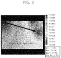
- FIG. 5 illustrates a temperature difference in a chip without heating elements
- FIG. 6 illustrates a temperature difference in a chip including heating elements, in accordance with an example embodiment
- FIG. 7 illustrates a flow chart illustrating a method for thermal dark shading reduction in a CMOS image sensor, in accordance with an example embodiment.
- FIG. 1 illustrates a schematic block diagram of a system 100 for thermal dark shading (or thermal shading or dark shading) reduction in a complementary metal-oxide-semiconductor (CMOS) image sensor, in accordance with an example embodiment.
- CMOS complementary metal-oxide-semiconductor
- the system 100 may be configured to reduce thermal dark shading in a CMOS image sensor 102 by embedding a plurality of heating elements 104 in the CMOS image sensor 102 .
- the system 100 may be implemented in mobile phones equipped with a camera, automotive image sensors, surveillance image sensors, and any large CMOS image sensor of higher resolution and/or large die size, etc.
- the system 100 includes the CMOS image sensor 102 , the plurality of heating elements 104 , and a controller 108 .
- the system 100 may also include a detector 106 .
- the detector 106 and the controller 108 are included in the CMOS image sensor 102 , but the disclosure is not limited thereto, and the detector 106 and the controller 108 may be provided separate from the CMS image sensor 102 and are electrically connected with the CMOS image sensor 102 .
- the CMOS image sensor 102 may be configured to capture an image.
- the CMOS image sensor 102 may be a one chip sensor, or a three-dimensional (3D) image sensor in which two or more chips are stacked.
- FIG. 2 illustrates an example in which two chips are stacked to provide a 3D image sensor 102 .
- the CMOS image sensor 102 may include a top chip 204 and a bottom chip 202 which are connected to each other (e.g., glued together).
- the top chip 204 of the CMOS image sensor 102 includes an array of active pixel sensor elements such as photodiodes, which convert photon signals to an electrical signal.
- the bottom chip 202 of the CMOS image sensor 102 contains a conversion circuitry which converts the electrical signal to a digital signal.
- the bottom chip 202 may include the plurality of heating elements 104 , the detector 106 , and the controller 108 .
- the plurality of heating elements 104 may be implemented in a form of a circuit, as shown in FIG. 3 .
- each of the plurality of heating elements 104 may include a resistor and a metal-oxide-semiconductor field-effect transistor (MOSFET).
- MOSFET metal-oxide-semiconductor field-effect transistor
- the plurality of heating elements 104 may include a resistor and a negative-channel metal-oxide semiconductor (NMOS) transistor serially connected to the resistor between a power supply (e.g., VDDD) and ground of the chip, and a plurality of branches of a resistor and an NMOS transistor are connected in parallel between the power supply and the ground.
- a power supply e.g., VDDD
- the NMOS transistor may be configured to act as a switching element in each branch of a resistor and an NMOS transistor of the plurality of heating elements 104 . Therefore, each of the plurality of heating elements 104 is controllable to be switched ON/OFF by the controller 108 by switching ON/OFF the NMOS transistor of each branch. For example, one branch (e.g. a branch including R2) may be activated and another branch (e.g. a branch including R4) may be switched-off by selectively switching an NMOS. Accordingly, heat generation of the plurality of heating elements 104 may be controlled.
- the power consumption of the plurality of heating elements 104 may be expressed as shown below, assuming that a voltage drop across the NMOS transistors is negligible:
- the plurality of heating elements 104 may be scattered across the conversion circuitry in the bottom chip 202 to balance thermal gradient in the bottom chip 202 .
- the thermal gradient in the bottom chip 202 of the image sensor 102 affects photosensitive elements in the top chip 204 .
- the plurality of heating elements 104 may also be implemented via various power consuming blocks such as an inverter chain, a ring oscillator or any power consuming block within a small area to produce localized heating.
- the detector 106 may be embedded in the bottom chip 202 of the image sensor 102 and may be configured to detect one or more regions across the CMOS image sensor 102 in which thermal shading occurs under low light conditions.
- the system may embed the detector 106 in the bottom chip 202 .
- the system 100 during the testing of the bottom chip 202 , may detect the one or more regions across the CMOS image sensor 102 in which thermal shading occurs under low light conditions and store information related to this detection. The information may be used in switching ON/OFF a subset of the plurality of heating elements 104 to provide localized heating within the CMOS image sensor.
- the controller 108 is linked to (or associated with) the image sensor 102 and the detector 106 .
- the controller 108 may be configured to automatically switch ON a subset of the plurality of heating elements 104 to provide localized heating within a region of the CMOS image sensor 102 in which thermal shading occurs under low light image capturing conditions.
- the controller 108 may be configured to automatically switch OFF the subset of heating elements 104 during an active power consumption phase of the CMOS image sensor 102 .
- the controller 108 may be implemented by a processor such as a micro control unit (MCU) or a central processing unit (CPU), firmware, or a hardware logic such as a field programmable gate array (FPGA), or any combination thereof.
- MCU micro control unit
- CPU central processing unit
- FPGA field programmable gate array
- FIG. 4 illustrates the power consumption of the CMOS image sensor 102 during an active period (or an active power consumption phase) and a low power phase, in accordance with an example embodiment.
- the subset of the heating elements 104 may be controlled to be switched on or off according to the requirement in the CMOS image sensor 102 .
- the subset of the heating elements 104 may be switched on during the low power phase of the sensor operation (e.g., vertical-blank phase).
- the low power phase of the CMOS image sensor 102 may enable higher light capture, and therefore, driving the subset of the plurality of heating elements 104 may not increase power consumption during a highest power consumption mode (e.g., bright light conditions).
- FIG. 5 shows a temperature difference in a chip without the heating elements 104
- FIG. 6 shows a temperature difference in a chip with the heating elements 104 , in accordance with an example embodiment.
- FIG. 7 illustrates a flow chart illustrating a method 700 for thermal dark shading reduction in a CMOS image sensor, in accordance with an example embodiment.
- FIG. 7 illustrates a flow chart illustrating a method 700 for thermal dark shading reduction in a CMOS image sensor, in accordance with an example embodiment.
- the method 700 includes embedding a plurality of heating elements in a CMOS image sensor in a chip.
- embedding includes generating a map of the plurality of heating elements in the chip.
- embedding further includes enabling a control for switching ON of the one or more heating elements from the plurality of heating elements with respect to the detected thermal dark shading region. For example, enabling a control for switching ON of the one or more heating elements may be performed by referring to the map of the plurality of heating elements.
- the method 700 includes detecting one or more regions across the CMOS image sensor in which thermal shading occurs under low light conditions.
- the detector 106 may be configured to detect one or more regions across the CMOS image sensor undergoing thermal shading during low light conditions
- the detecting of the thermal dark shading region across the CMOS image sensor includes at least one selected from scattering a plurality of temperature sensors across the chip to detect a temperature difference across the chip, and capturing a dark image to detect the thermal dark shading region across the CMOS image sensor. Further, detecting the thermal dark shading region across the CMOS image sensor may also include processing images of the CMOS image sensor to detect the thermal dark shading region using artificial intelligence (AI) and/or machine learning.
- AI artificial intelligence
- the method 700 includes automatically switching ON a subset of the heating elements for providing localized heating within the CMOS image sensor based on the one or more regions undergoing thermal shading under low light image capturing conditions.
- the method 700 includes automatically switching OFF the subset of heating elements during an active power consumption phase of the CMOS image sensor.
- the controller 108 may be configured to automatically switch ON a subset of the heating elements for providing localized heating within the CMOS image sensor based on the regions undergoing thermal shading during low light image capturing conditions and automatically switch OFF the subset of heating elements during an active power consumption phase of the CMOS image sensor.
- localized heating is triggered by power consumption due to the thermal resistance.
- the disclosure achieves at least leads to the following advantages:
- Each heating element uses a very small area
- a circuit of each heating element is based on already available components in a fabrication process
- At least one of the components, elements, modules or units described herein may be embodied as various numbers of hardware, software and/or firmware structures that execute respective functions described above, according to an example embodiment.
- at least one of these components, elements or units may use a direct circuit structure, such as a memory, a processor, a logic circuit, a look-up table, etc. that may execute the respective functions through controls of one or more microprocessors or other control apparatuses.
- at least one of these components, elements or units may be specifically embodied by a module, a program, or a part of code, which contains one or more executable instructions for performing specified logic functions, and executed by one or more microprocessors or other control apparatuses.
- At least one of these components, elements or units may further include or implemented by a processor such as a central processing unit (CPU) that performs the respective functions, a microprocessor, or the like.
- a processor such as a central processing unit (CPU) that performs the respective functions, a microprocessor, or the like.
- CPU central processing unit
- Two or more of these components, elements or units may be combined into one single component, element or unit which performs all operations or functions of the combined two or more components, elements of units.
- at least part of functions of at least one of these components, elements or units may be performed by another of these components, element or units.
- a bus is not illustrated in the block diagrams, communication between the components, elements or units may be performed through the bus.
- Functional aspects of the above example embodiments may be implemented in algorithms that execute on one or more processors.
- the components, elements or units represented by a block or processing steps may employ any number of related art techniques for electronics configuration, signal processing and/or control, data processing and the like.
Landscapes
- Engineering & Computer Science (AREA)
- Multimedia (AREA)
- Signal Processing (AREA)
- Software Systems (AREA)
- Theoretical Computer Science (AREA)
- Computer Vision & Pattern Recognition (AREA)
- Evolutionary Computation (AREA)
- Medical Informatics (AREA)
- Data Mining & Analysis (AREA)
- Physics & Mathematics (AREA)
- Computing Systems (AREA)
- General Engineering & Computer Science (AREA)
- General Physics & Mathematics (AREA)
- Mathematical Physics (AREA)
- Artificial Intelligence (AREA)
- Transforming Light Signals Into Electric Signals (AREA)
- Solid State Image Pick-Up Elements (AREA)
- Semiconductor Integrated Circuits (AREA)
Abstract
Description
Claims (18)
Applications Claiming Priority (2)
| Application Number | Priority Date | Filing Date | Title |
|---|---|---|---|
| IN201941033238 | 2019-08-17 | ||
| IN201941033238 | 2019-08-17 |
Publications (2)
| Publication Number | Publication Date |
|---|---|
| US20210051289A1 US20210051289A1 (en) | 2021-02-18 |
| US11375144B2 true US11375144B2 (en) | 2022-06-28 |
Family
ID=74567656
Family Applications (1)
| Application Number | Title | Priority Date | Filing Date |
|---|---|---|---|
| US16/994,294 Active US11375144B2 (en) | 2019-08-17 | 2020-08-14 | Method and system for reducing thermal shading in image sensor using on chip localized heat source |
Country Status (3)
| Country | Link |
|---|---|
| US (1) | US11375144B2 (en) |
| KR (1) | KR20210021271A (en) |
| CN (1) | CN112399102B (en) |
Families Citing this family (1)
| Publication number | Priority date | Publication date | Assignee | Title |
|---|---|---|---|---|
| KR20230018839A (en) * | 2021-07-30 | 2023-02-07 | 에스케이하이닉스 주식회사 | Image sensing device and method of operating the image sensing device |
Citations (7)
| Publication number | Priority date | Publication date | Assignee | Title |
|---|---|---|---|---|
| US20110089517A1 (en) | 2009-10-20 | 2011-04-21 | Omnivision Technologies, Inc. | Cmos image sensor with heat management structures |
| US20130218500A1 (en) * | 2012-02-22 | 2013-08-22 | Ulis | Method for correcting the drift of an infrared radiation detector comprising an array of resistive imaging bolometers and device implementing such a method |
| WO2015157374A1 (en) | 2014-04-08 | 2015-10-15 | Qualcomm Incorporated | Energy efficiency aware thermal management in a multi-processor system on a chip |
| US9282259B2 (en) * | 2012-12-10 | 2016-03-08 | Fluke Corporation | Camera and method for thermal image noise reduction using post processing techniques |
| US9318528B2 (en) | 2013-03-15 | 2016-04-19 | Taiwan Semiconductor Manufacturing Company, Ltd. | Image sensor device and method |
| US20190089872A1 (en) * | 2017-09-19 | 2019-03-21 | Google Llc | Temperature-Controlled Camera Assembly |
| US10451487B1 (en) * | 2018-08-23 | 2019-10-22 | Raytheon Company | Per-pixel dark reference bolometer |
Family Cites Families (4)
| Publication number | Priority date | Publication date | Assignee | Title |
|---|---|---|---|---|
| JPH05206423A (en) * | 1992-01-27 | 1993-08-13 | Sony Corp | Solid-state image sensing device |
| US8384395B2 (en) * | 2010-05-06 | 2013-02-26 | Texas Instrument Incorporated | Circuit for controlling temperature and enabling testing of a semiconductor chip |
| JP2013106185A (en) * | 2011-11-14 | 2013-05-30 | Canon Inc | Solid-state imaging device and image processing device using the same |
| KR102471159B1 (en) * | 2015-10-12 | 2022-11-25 | 삼성전자주식회사 | Imgage sensor and method of manufacturing the same |
-
2020
- 2020-08-11 KR KR1020200100652A patent/KR20210021271A/en active Pending
- 2020-08-14 US US16/994,294 patent/US11375144B2/en active Active
- 2020-08-17 CN CN202010823544.3A patent/CN112399102B/en active Active
Patent Citations (7)
| Publication number | Priority date | Publication date | Assignee | Title |
|---|---|---|---|---|
| US20110089517A1 (en) | 2009-10-20 | 2011-04-21 | Omnivision Technologies, Inc. | Cmos image sensor with heat management structures |
| US20130218500A1 (en) * | 2012-02-22 | 2013-08-22 | Ulis | Method for correcting the drift of an infrared radiation detector comprising an array of resistive imaging bolometers and device implementing such a method |
| US9282259B2 (en) * | 2012-12-10 | 2016-03-08 | Fluke Corporation | Camera and method for thermal image noise reduction using post processing techniques |
| US9318528B2 (en) | 2013-03-15 | 2016-04-19 | Taiwan Semiconductor Manufacturing Company, Ltd. | Image sensor device and method |
| WO2015157374A1 (en) | 2014-04-08 | 2015-10-15 | Qualcomm Incorporated | Energy efficiency aware thermal management in a multi-processor system on a chip |
| US20190089872A1 (en) * | 2017-09-19 | 2019-03-21 | Google Llc | Temperature-Controlled Camera Assembly |
| US10451487B1 (en) * | 2018-08-23 | 2019-10-22 | Raytheon Company | Per-pixel dark reference bolometer |
Also Published As
| Publication number | Publication date |
|---|---|
| CN112399102A (en) | 2021-02-23 |
| KR20210021271A (en) | 2021-02-25 |
| US20210051289A1 (en) | 2021-02-18 |
| CN112399102B (en) | 2024-12-27 |
Similar Documents
| Publication | Publication Date | Title |
|---|---|---|
| US12041382B2 (en) | Imaging device, imaging system, vehicle running control system, and image processing device | |
| US8730330B2 (en) | Image sensors with dark pixels for real-time verification of imaging systems | |
| US9030583B2 (en) | Imaging system with foveated imaging capabilites | |
| US8013915B2 (en) | Anti-eclipsing circuit for image sensors | |
| US9131211B2 (en) | Imaging systems with verification pixels | |
| US20180241953A1 (en) | Methods and apparatus for pixel binning and readout | |
| US9897482B2 (en) | Photoelectric conversion apparatus and image pickup system having photoelectric conversion apparatus | |
| US10313610B2 (en) | Image sensors with dynamic pixel binning | |
| US20150281684A1 (en) | Imaging systems with pixel array verification circuitry | |
| US9407848B2 (en) | Method and apparatus for pixel control signal verification | |
| US20060097132A1 (en) | CMOS image sensor and related method of operation | |
| US11375144B2 (en) | Method and system for reducing thermal shading in image sensor using on chip localized heat source | |
| EP1908278B1 (en) | Image sensor architecture employing one or more floating gate devices | |
| US8698089B2 (en) | Photo detecting pixels and X-ray detector including the same | |
| US7738019B2 (en) | System and method for providing automatic gain control in an imaging device | |
| US10687006B2 (en) | Photodiode limiter | |
| US20030090583A1 (en) | Photosensor system and drive control method for the same | |
| US7710481B2 (en) | Image sensor architecture employing one or more non-volatile memory cells | |
| US12219075B2 (en) | Detection device | |
| US20200120257A1 (en) | Method for processing signals from an imaging device, and associated device | |
| WO2006049605A1 (en) | Image sensor and method with multiple scanning modes | |
| KR20160023272A (en) | Unit pixel timing control method of Imaging device having WDR pixel array of 1PD structure |
Legal Events
| Date | Code | Title | Description |
|---|---|---|---|
| AS | Assignment |
Owner name: SAMSUNG ELECTRONICS CO., LTD., KOREA, REPUBLIC OF Free format text: ASSIGNMENT OF ASSIGNORS INTEREST;ASSIGNORS:CHOWDHURY, ANKUSH;LALAM, RAMANA BABU;RUPAPARA, PRASHANT GOVINDLAL;AND OTHERS;REEL/FRAME:053504/0520 Effective date: 20200813 |
|
| FEPP | Fee payment procedure |
Free format text: ENTITY STATUS SET TO UNDISCOUNTED (ORIGINAL EVENT CODE: BIG.); ENTITY STATUS OF PATENT OWNER: LARGE ENTITY |
|
| STPP | Information on status: patent application and granting procedure in general |
Free format text: DOCKETED NEW CASE - READY FOR EXAMINATION |
|
| FEPP | Fee payment procedure |
Free format text: PETITION RELATED TO MAINTENANCE FEES GRANTED (ORIGINAL EVENT CODE: PTGR); ENTITY STATUS OF PATENT OWNER: LARGE ENTITY |
|
| STPP | Information on status: patent application and granting procedure in general |
Free format text: NON FINAL ACTION MAILED |
|
| STPP | Information on status: patent application and granting procedure in general |
Free format text: RESPONSE TO NON-FINAL OFFICE ACTION ENTERED AND FORWARDED TO EXAMINER |
|
| STPP | Information on status: patent application and granting procedure in general |
Free format text: NOTICE OF ALLOWANCE MAILED -- APPLICATION RECEIVED IN OFFICE OF PUBLICATIONS |
|
| STPP | Information on status: patent application and granting procedure in general |
Free format text: PUBLICATIONS -- ISSUE FEE PAYMENT VERIFIED |
|
| STCF | Information on status: patent grant |
Free format text: PATENTED CASE |
|
| MAFP | Maintenance fee payment |
Free format text: PAYMENT OF MAINTENANCE FEE, 4TH YEAR, LARGE ENTITY (ORIGINAL EVENT CODE: M1551); ENTITY STATUS OF PATENT OWNER: LARGE ENTITY Year of fee payment: 4 |