US11331663B2 - Microfluidic component package - Google Patents
Microfluidic component package Download PDFInfo
- Publication number
- US11331663B2 US11331663B2 US16/168,020 US201816168020A US11331663B2 US 11331663 B2 US11331663 B2 US 11331663B2 US 201816168020 A US201816168020 A US 201816168020A US 11331663 B2 US11331663 B2 US 11331663B2
- Authority
- US
- United States
- Prior art keywords
- microfluidic
- component package
- enclosure
- microfluidic component
- cavity
- Prior art date
- Legal status (The legal status is an assumption and is not a legal conclusion. Google has not performed a legal analysis and makes no representation as to the accuracy of the status listed.)
- Active, expires
Links
Images

Classifications
-
- B—PERFORMING OPERATIONS; TRANSPORTING
- B01—PHYSICAL OR CHEMICAL PROCESSES OR APPARATUS IN GENERAL
- B01L—CHEMICAL OR PHYSICAL LABORATORY APPARATUS FOR GENERAL USE
- B01L3/00—Containers or dishes for laboratory use, e.g. laboratory glassware; Droppers
- B01L3/50—Containers for the purpose of retaining a material to be analysed, e.g. test tubes
- B01L3/502—Containers for the purpose of retaining a material to be analysed, e.g. test tubes with fluid transport, e.g. in multi-compartment structures
- B01L3/5027—Containers for the purpose of retaining a material to be analysed, e.g. test tubes with fluid transport, e.g. in multi-compartment structures by integrated microfluidic structures, i.e. dimensions of channels and chambers are such that surface tension forces are important, e.g. lab-on-a-chip
- B01L3/502707—Containers for the purpose of retaining a material to be analysed, e.g. test tubes with fluid transport, e.g. in multi-compartment structures by integrated microfluidic structures, i.e. dimensions of channels and chambers are such that surface tension forces are important, e.g. lab-on-a-chip characterised by the manufacture of the container or its components
-
- B—PERFORMING OPERATIONS; TRANSPORTING
- B01—PHYSICAL OR CHEMICAL PROCESSES OR APPARATUS IN GENERAL
- B01L—CHEMICAL OR PHYSICAL LABORATORY APPARATUS FOR GENERAL USE
- B01L9/00—Supporting devices; Holding devices
- B01L9/52—Supports specially adapted for flat sample carriers, e.g. for plates, slides, chips
- B01L9/527—Supports specially adapted for flat sample carriers, e.g. for plates, slides, chips for microfluidic devices, e.g. used for lab-on-a-chip
-
- B—PERFORMING OPERATIONS; TRANSPORTING
- B23—MACHINE TOOLS; METAL-WORKING NOT OTHERWISE PROVIDED FOR
- B23K—SOLDERING OR UNSOLDERING; WELDING; CLADDING OR PLATING BY SOLDERING OR WELDING; CUTTING BY APPLYING HEAT LOCALLY, e.g. FLAME CUTTING; WORKING BY LASER BEAM
- B23K1/00—Soldering, e.g. brazing, or unsoldering
- B23K1/0008—Soldering, e.g. brazing, or unsoldering specially adapted for particular articles or work
- B23K1/0016—Soldering of electronic components
-
- B—PERFORMING OPERATIONS; TRANSPORTING
- B81—MICROSTRUCTURAL TECHNOLOGY
- B81B—MICROSTRUCTURAL DEVICES OR SYSTEMS, e.g. MICROMECHANICAL DEVICES
- B81B7/00—Microstructural systems ; Auxiliary parts of microstructural devices or systems
- B81B7/0032—Packages or encapsulation
- B81B7/0061—Packages or encapsulation suitable for fluid transfer from the MEMS out of the package or vice versa, e.g. transfer of liquid, gas, sound
-
- B—PERFORMING OPERATIONS; TRANSPORTING
- B81—MICROSTRUCTURAL TECHNOLOGY
- B81C—PROCESSES OR APPARATUS SPECIALLY ADAPTED FOR THE MANUFACTURE OR TREATMENT OF MICROSTRUCTURAL DEVICES OR SYSTEMS
- B81C1/00—Manufacture or treatment of devices or systems in or on a substrate
- B81C1/00015—Manufacture or treatment of devices or systems in or on a substrate for manufacturing microsystems
- B81C1/00261—Processes for packaging MEMS devices
- B81C1/00309—Processes for packaging MEMS devices suitable for fluid transfer from the MEMS out of the package or vice versa, e.g. transfer of liquid, gas, sound
-
- B—PERFORMING OPERATIONS; TRANSPORTING
- B01—PHYSICAL OR CHEMICAL PROCESSES OR APPARATUS IN GENERAL
- B01L—CHEMICAL OR PHYSICAL LABORATORY APPARATUS FOR GENERAL USE
- B01L2200/00—Solutions for specific problems relating to chemical or physical laboratory apparatus
- B01L2200/02—Adapting objects or devices to another
- B01L2200/026—Fluid interfacing between devices or objects, e.g. connectors, inlet details
- B01L2200/027—Fluid interfacing between devices or objects, e.g. connectors, inlet details for microfluidic devices
-
- B—PERFORMING OPERATIONS; TRANSPORTING
- B01—PHYSICAL OR CHEMICAL PROCESSES OR APPARATUS IN GENERAL
- B01L—CHEMICAL OR PHYSICAL LABORATORY APPARATUS FOR GENERAL USE
- B01L2200/00—Solutions for specific problems relating to chemical or physical laboratory apparatus
- B01L2200/06—Fluid handling related problems
- B01L2200/0689—Sealing
-
- B—PERFORMING OPERATIONS; TRANSPORTING
- B01—PHYSICAL OR CHEMICAL PROCESSES OR APPARATUS IN GENERAL
- B01L—CHEMICAL OR PHYSICAL LABORATORY APPARATUS FOR GENERAL USE
- B01L2400/00—Moving or stopping fluids
- B01L2400/06—Valves, specific forms thereof
- B01L2400/0677—Valves, specific forms thereof phase change valves; Meltable, freezing, dissolvable plugs; Destructible barriers
-
- B—PERFORMING OPERATIONS; TRANSPORTING
- B01—PHYSICAL OR CHEMICAL PROCESSES OR APPARATUS IN GENERAL
- B01L—CHEMICAL OR PHYSICAL LABORATORY APPARATUS FOR GENERAL USE
- B01L3/00—Containers or dishes for laboratory use, e.g. laboratory glassware; Droppers
- B01L3/50—Containers for the purpose of retaining a material to be analysed, e.g. test tubes
- B01L3/502—Containers for the purpose of retaining a material to be analysed, e.g. test tubes with fluid transport, e.g. in multi-compartment structures
- B01L3/5027—Containers for the purpose of retaining a material to be analysed, e.g. test tubes with fluid transport, e.g. in multi-compartment structures by integrated microfluidic structures, i.e. dimensions of channels and chambers are such that surface tension forces are important, e.g. lab-on-a-chip
- B01L3/502715—Containers for the purpose of retaining a material to be analysed, e.g. test tubes with fluid transport, e.g. in multi-compartment structures by integrated microfluidic structures, i.e. dimensions of channels and chambers are such that surface tension forces are important, e.g. lab-on-a-chip characterised by interfacing components, e.g. fluidic, electrical, optical or mechanical interfaces
-
- B—PERFORMING OPERATIONS; TRANSPORTING
- B23—MACHINE TOOLS; METAL-WORKING NOT OTHERWISE PROVIDED FOR
- B23K—SOLDERING OR UNSOLDERING; WELDING; CLADDING OR PLATING BY SOLDERING OR WELDING; CUTTING BY APPLYING HEAT LOCALLY, e.g. FLAME CUTTING; WORKING BY LASER BEAM
- B23K2101/00—Articles made by soldering, welding or cutting
- B23K2101/36—Electric or electronic devices
- B23K2101/42—Printed circuits
-
- B—PERFORMING OPERATIONS; TRANSPORTING
- B81—MICROSTRUCTURAL TECHNOLOGY
- B81B—MICROSTRUCTURAL DEVICES OR SYSTEMS, e.g. MICROMECHANICAL DEVICES
- B81B2201/00—Specific applications of microelectromechanical systems
- B81B2201/05—Microfluidics
- B81B2201/058—Microfluidics not provided for in B81B2201/051 - B81B2201/054
-
- B—PERFORMING OPERATIONS; TRANSPORTING
- B81—MICROSTRUCTURAL TECHNOLOGY
- B81C—PROCESSES OR APPARATUS SPECIALLY ADAPTED FOR THE MANUFACTURE OR TREATMENT OF MICROSTRUCTURAL DEVICES OR SYSTEMS
- B81C2203/00—Forming microstructural systems
- B81C2203/01—Packaging MEMS
- B81C2203/0172—Seals
-
- B—PERFORMING OPERATIONS; TRANSPORTING
- B81—MICROSTRUCTURAL TECHNOLOGY
- B81C—PROCESSES OR APPARATUS SPECIALLY ADAPTED FOR THE MANUFACTURE OR TREATMENT OF MICROSTRUCTURAL DEVICES OR SYSTEMS
- B81C2203/00—Forming microstructural systems
- B81C2203/03—Bonding two components
- B81C2203/033—Thermal bonding
- B81C2203/035—Soldering
Definitions
- the subject matter described herein relates generally to microfluidic systems and their manufacture, and more specifically the packaging of devices that can interact with small volumes of fluid for the purpose of embedding them within microfluidic systems.
- Microfluidic systems are of use for applications where small quantities of fluid need to be manipulated and controlled. Two common applications are 1) for high throughput analysis, where large numbers of small volume experiments are performed; and 2) point of care analysis, where an assay is to be performed on a small liquid sample such as blood or saliva. While microfluidics has shown great promise for these applications, a significant problem exists for the integration of microfluidic functions with other common functions, such as mechanical, optical, and electrical functions. A truly useful system must integrate these disparate functions together into a single device.
- microfluidic production approaches produce capillary systems in polymer, glass, or other materials using embossing or etch methods. These methods are efficient at producing microfluidic channels, but they are poor for integrating electronics, optics, and mechanical functions into the same system. Usually, these non-fluidic functions are added as external components after the microfluidics have been produced. In some cases, attempts are made to include these functions during the manufacture of the microfluidic channels; however, this results in highly complex and expensive manufacturing processes that are not suitable for large-scale production.
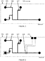
- FIG. 1 shows an example of a conventional microfluidic device which comprises a flat substrate 101 , typically comprising plastic or glass, with openings 103 to allow fluid to be introduced and extracted from a network of micro-channels 105 , or capillaries, whose function is to move fluid from one location to another.
- Some of the micro-channels 107 are constructed in such a manner to provide additional functionality to the device, such as heating, valving or pumping. These parts are manufactured in the same process as the manufacture of the micro-channels. Most of the fluidic functions are provided externally 109 to the device.
- FIG. 2 shows an example of a conventional microfluidic device including discrete components.
- the microfluidic device comprises a flat substrate 201 , typically comprising plastic or glass, with openings 203 to allow fluid to be introduced and extracted from a network of micro-channels 205 , or capillaries, whose function is to move fluid from one location to another.
- Discrete components 207 , 209 are attached or embedded within the device in such a manner to access the fluid in the micro-channels and provide functionality.
- Components, such as, e.g., the component 209 connect with the microfluidic channels, but may also connect with external systems, such as electrical traces 211 .
- the components need to be connected to one or more microfluidic channels, and may require other connections such as electrical, optical, mechanical, or thermal connections.
- connections such as electrical, optical, mechanical, or thermal connections.
- microfluidic component package that enables a microfluidic device to be fixed to a printed circuit board or other substrate, and embedded within a larger microfluidic system.
- Microfluidic components enable conventional microelectronic infrastructure and technology to be merged with microfluidic systems.
- the embodiments presented are herein referred to as a “microfluidic component package” or MFCP.
- a microfluidic component comprises a small device intended to be embedded within a microfluidic system.
- the component typically comprises one or more ports that allow the component to come in contact with fluid that is routed on a microfluidic layer, and to perform a function that is useful to the operation of the microfluidic system.
- the device is manufactured by any means that is reasonable.
- Microfluidic components may perform operations such as micro-pumps, micro-valves, micro-heaters, micro-electrodes, micro-sensors, etc.
- a microfluidic component package (MFCP) allows a device to be readily integrated with the microfluidic system.
- the MFCP is small enough to be mounted on a printed circuit board or other surface. It is comprised of molded polymer which houses or encapsulates one or more microfluidic devices, and has one or more access openings, or ports, to allow fluid to enter the package and interact with the enclosed device. The ports are temporarily sealed to allow the MFCP to be handled and assembled using automation technology during production of the system, but are opened after the MFCP has been embedded within the microfluidic system.
- FIG. 1 is a schematic of microfluidic system has micro-channels and active parts that operate as valves, pumps, and similar functions. These are all fabricated at the same time, in the same substrate, as the microfluidics.
- FIG. 2 is a schematic of microfluidic system that utilizes individual devices that are manufactured separately and then embedded within the system when manufacturing the microfluidics.
- FIG. 3 is a cross-sectional view of an exemplary microfluidic component package MFCP with multiple devices and ports, according to embodiments of the present disclosure.
- FIG. 4 is a cross-sectional view of MFCP embedded within a microfluidic system and electronic circuit board, according to embodiments of the present disclosure.
- FIG. 5A illustrates a first step in an exemplary MFCP embedding process, according to embodiments of the present disclosure.
- FIG. 5B illustrates a second step in an exemplary MFCP embedding process, according to embodiments of the present disclosure.
- FIG. 5C illustrates a third step in an exemplary MFCP embedding process, according to embodiments of the present disclosure.
- FIG. 5D illustrates a fourth step in an exemplary MFCP embedding process, according to embodiments of the present disclosure.
- the various embodiments provided herein are generally directed to a microfluidic component package (“MFCP”) that can produce a consistent interface between a small microfluidic device and a larger microfluidic system, while also allowing access to electrical, optical, mechanical, and thermal connections.
- the MFCP may comprise one or more microfluidic devices contained within it, and the MFCP is intended to be embedded within a larger microfluidic system.
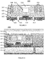
- FIG. 3 shows an exemplary MFCP 300 , according to embodiments of the present disclosure.
- the MFCP 300 comprises an enclosure 301 which may be solid filled or may comprise a hollow interior.
- the enclosure 301 may be paired with a substrate 303 on one or more sides, for example the bottom, to add additional functionality to the package or to assist in attachment to a larger system.
- Within the enclosure 301 are one or more microfluidic elements that add functionality to a microfluidic system such as micro-channels 305 .
- the micro-channels 305 are encapsulated within the package or enclosure 301 .
- One or more ports 309 and 315 may be defined to allow access to the microfluidic elements/micro-channels 305 inside the enclosure 301 .
- a sacrificial material 307 may be used to connect a microfluidic element to the port of the package.
- the sacrificial material 307 is known to be dissolvable or etchable by a suitable chemical.
- a physical connection can be made from the port to the microfluidic element by first making an opening in the enclosure 301 at the location of the port 309 , 315 , then removing the sacrificial material 307 by dissolving or etching the sacrificial material 307 away using an appropriate chemical. This provides an opening between the outside of the package and the microfluidic elements 305 inside.
- the enclosure 301 may include cavities 311 , and may provide optical openings 313 , such as lenses, filters, mirrors, and the like. Ports 315 may be used to provide access to other features of the enclosed device, such as pneumatic, hydraulic, mechanical, or thermal access. Ports may be provided on all sides of the enclosure, including ports 317 through the bottom substrate.
- the enclosure 301 may include elements 319 in addition to microfluidic elements, such as microelectronic devices, including light sources, photosensors, computers, and electronics.
- the enclosure 301 may also include features that allow it to be attached to conventional systems, such as tapped holes 321 for screws or contact pads 323 for soldering the device 300 to a printed circuit board.
- the contact pads 323 also allow electrical energy to enter and leave the package.
- MFCP may be embedded within any microfluidic system.
- a microfluidic system for embedding the MFCP within comprises a network of microfluidic channels prepared on a printed circuit board.
- FIG. 4 shows the preferred method for embedding the MFCP in a larger microfluidic system 400 .
- a printed circuit board (PCB) 401 is prepared having a solid material and electrical traces for routing electrical signals.
- the PCB 401 comprises specific contact pads 403 for connecting to a component such as an MFCP 409 .
- Mounting is most commonly performed using solder 405 , which connects the contact pads from the PCB 403 with the contact pads 407 on the MFCP 409 .
- the solder connections 405 provide electrical connection as well as mechanical connection.
- the MFCP 409 that comprises the microfluidic and other elements is encapsulated within a material 411 (e.g., polymer). Openings 413 are provided in the encapsulating material (e.g., polymer) 411 to allow fluidic access from a microfluidic channel 415 to the ports of the MFCP 409 . Microfluidic channels 415 are fabricated on the encapsulating material (e.g., polymer) 411 forming the larger microfluidic system 400 .
- a material 411 e.g., polymer
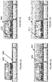
- FIGS. 5A-5D illustrate how an MFCP 501 may be embedded within a printed circuit board and microfluidic system.
- FIG. 5A illustrates a first step in an exemplary MFCP embedding process, according to embodiments of the present disclosure.
- the MFCP 501 is mounted on a printed circuit board 503 using technology such as soldering.
- FIG. 5B illustrates a second step in an exemplary MFCP embedding process, according to embodiments of the present disclosure.
- an encapsulating polymer 505 is used to cover the MFCP 501 and printed circuit board 503 .
- the encapsulating polymer 505 is embossed or planarized to produce a suitable surface, for example, a flat surface 507 .
- FIG. 5C illustrates a third step in an exemplary MFCP embedding process, according to embodiments of the present disclosure. As shown in FIG. 5C , one or more holes 509 are drilled through the encapsulating polymer 505 to produce openings in the package and expose the sacrificial material 502 within.
- FIG. 5D illustrates a fourth step in an exemplary MFCP embedding process, according to embodiments of the present disclosure.
- the sacrificial material 502 is removed by dissolution or etching 511 , opening up the microfluidic elements within the package.
- a microfluidic layer 513 is bonded to the encapsulating material to form a sealed microfluidic system.
Landscapes
- Engineering & Computer Science (AREA)
- Chemical & Material Sciences (AREA)
- Microelectronics & Electronic Packaging (AREA)
- Health & Medical Sciences (AREA)
- Analytical Chemistry (AREA)
- Clinical Laboratory Science (AREA)
- Chemical Kinetics & Catalysis (AREA)
- Dispersion Chemistry (AREA)
- Hematology (AREA)
- General Health & Medical Sciences (AREA)
- Manufacturing & Machinery (AREA)
- Computer Hardware Design (AREA)
- Mechanical Engineering (AREA)
- Micromachines (AREA)
Abstract
Description
Claims (12)
Priority Applications (1)
| Application Number | Priority Date | Filing Date | Title |
|---|---|---|---|
| US16/168,020 US11331663B2 (en) | 2016-05-31 | 2018-10-23 | Microfluidic component package |
Applications Claiming Priority (3)
| Application Number | Priority Date | Filing Date | Title |
|---|---|---|---|
| US201662343169P | 2016-05-31 | 2016-05-31 | |
| PCT/US2017/035056 WO2017210219A1 (en) | 2016-05-31 | 2017-05-30 | Microfluidic component package |
| US16/168,020 US11331663B2 (en) | 2016-05-31 | 2018-10-23 | Microfluidic component package |
Related Parent Applications (1)
| Application Number | Title | Priority Date | Filing Date |
|---|---|---|---|
| PCT/US2017/035056 Continuation WO2017210219A1 (en) | 2016-05-31 | 2017-05-30 | Microfluidic component package |
Publications (2)
| Publication Number | Publication Date |
|---|---|
| US20190321821A1 US20190321821A1 (en) | 2019-10-24 |
| US11331663B2 true US11331663B2 (en) | 2022-05-17 |
Family
ID=60477825
Family Applications (1)
| Application Number | Title | Priority Date | Filing Date |
|---|---|---|---|
| US16/168,020 Active 2037-07-05 US11331663B2 (en) | 2016-05-31 | 2018-10-23 | Microfluidic component package |
Country Status (2)
| Country | Link |
|---|---|
| US (1) | US11331663B2 (en) |
| WO (1) | WO2017210219A1 (en) |
Citations (8)
| Publication number | Priority date | Publication date | Assignee | Title |
|---|---|---|---|---|
| US6443179B1 (en) * | 2001-02-21 | 2002-09-03 | Sandia Corporation | Packaging of electro-microfluidic devices |
| US6586885B2 (en) * | 2001-08-20 | 2003-07-01 | Motorola, Inc. | MHCD and microfluidic apparatus and method |
| US7004198B1 (en) * | 2004-07-20 | 2006-02-28 | Sandia Corporation | Micro-fluidic interconnect |
| US20070003434A1 (en) * | 2005-07-01 | 2007-01-04 | Honeywell International Inc. | Flow metered analyzer |
| WO2007107901A2 (en) * | 2006-03-20 | 2007-09-27 | Koninklijke Philips Electronics N.V. | A system-in-package platform for electronic-microfluidic devices |
| US20120267239A1 (en) * | 2011-04-20 | 2012-10-25 | Samson Chen | Single-layer pcb microfluidics |
| US20150182967A1 (en) * | 2013-12-31 | 2015-07-02 | Canon U.S. Life Sciences, Inc. | Printed circuit board designs for laminated microfluidic devices |
| US9101929B2 (en) * | 2010-03-18 | 2015-08-11 | Robert Bosch Gmbh | Microfluidic system for purposes of analysis and diagnosis and corresponding method for producing a microfluidic system |
Family Cites Families (3)
| Publication number | Priority date | Publication date | Assignee | Title |
|---|---|---|---|---|
| US6786708B2 (en) * | 2002-07-18 | 2004-09-07 | The Regents Of The University Of Michigan | Laminated devices and methods of making same |
| EP1884188A1 (en) * | 2006-08-02 | 2008-02-06 | F.Hoffmann-La Roche Ag | Packaging for an object with a hydrophilic surface coating |
| EP3089823A4 (en) * | 2013-12-31 | 2017-12-20 | Canon U.S. Life Sciences, Inc. | Field deployable small format fast first result microfluidic system |
-
2017
- 2017-05-30 WO PCT/US2017/035056 patent/WO2017210219A1/en not_active Ceased
-
2018
- 2018-10-23 US US16/168,020 patent/US11331663B2/en active Active
Patent Citations (8)
| Publication number | Priority date | Publication date | Assignee | Title |
|---|---|---|---|---|
| US6443179B1 (en) * | 2001-02-21 | 2002-09-03 | Sandia Corporation | Packaging of electro-microfluidic devices |
| US6586885B2 (en) * | 2001-08-20 | 2003-07-01 | Motorola, Inc. | MHCD and microfluidic apparatus and method |
| US7004198B1 (en) * | 2004-07-20 | 2006-02-28 | Sandia Corporation | Micro-fluidic interconnect |
| US20070003434A1 (en) * | 2005-07-01 | 2007-01-04 | Honeywell International Inc. | Flow metered analyzer |
| WO2007107901A2 (en) * | 2006-03-20 | 2007-09-27 | Koninklijke Philips Electronics N.V. | A system-in-package platform for electronic-microfluidic devices |
| US9101929B2 (en) * | 2010-03-18 | 2015-08-11 | Robert Bosch Gmbh | Microfluidic system for purposes of analysis and diagnosis and corresponding method for producing a microfluidic system |
| US20120267239A1 (en) * | 2011-04-20 | 2012-10-25 | Samson Chen | Single-layer pcb microfluidics |
| US20150182967A1 (en) * | 2013-12-31 | 2015-07-02 | Canon U.S. Life Sciences, Inc. | Printed circuit board designs for laminated microfluidic devices |
Non-Patent Citations (1)
| Title |
|---|
| Amy Wu, et al., "Modular integration of electronics and microfluidic systems using flexible printed circuit boards", 2010, Lab Chip, 10, 519-521 (Year: 2010). * |
Also Published As
| Publication number | Publication date |
|---|---|
| WO2017210219A1 (en) | 2017-12-07 |
| US20190321821A1 (en) | 2019-10-24 |
Similar Documents
| Publication | Publication Date | Title |
|---|---|---|
| JP5643880B2 (en) | MEMS device and manufacturing method thereof | |
| US7217588B2 (en) | Integrated MEMS packaging | |
| CN101405084B (en) | A system-in-package platform for electronic-microfluidic devices | |
| US20020134907A1 (en) | Polymer-based platform for microfluidic systems | |
| EP1884994B1 (en) | Semiconductor device and method of manufacturing the same | |
| EP3018092A1 (en) | MEMS package | |
| JP2008132587A (en) | Manufacturing method of wafer level vacuum package device | |
| CN106449498B (en) | For shifting the transposition head of microcomponent and the transfer method of microcomponent | |
| US11241687B2 (en) | Compact glass-based fluid analysis device and method to fabricate | |
| CN101875481A (en) | A MEMS packaging method based on low temperature co-fired ceramics | |
| TW201541579A (en) | Low cost package for fluid and device integration | |
| CN102371194B (en) | Manufacture the method for microfluid system | |
| US11331663B2 (en) | Microfluidic component package | |
| US6917099B2 (en) | Die carrier with fluid chamber | |
| CN111517271B (en) | Method including panel bonding operation and electronic device including cavity | |
| CN100536097C (en) | Method for interconnecting and packaging biomedical devices with electronic and fluidic functions | |
| CN111566801A (en) | Microfluidic chip with one or more vias | |
| WO2008030088A2 (en) | Assembly of at least one microfluidic device and a mounting piece, mounting piece and methods for manufacture and use of such an assembly | |
| US20200406255A1 (en) | Microfluidic Device | |
| JP2019093377A (en) | Fluid chip, fluid device and method for manufacturing therefor | |
| CN109748235B (en) | Semiconductor device, manufacturing process of sealed cavity of semiconductor device and pattern transfer plate | |
| CN109415199B (en) | Microfluidic device with manifold | |
| Wu et al. | A printed circuit board based microfluidic system for point-of-care diagnostics applications | |
| Dumbravescu | Reliable electrical interconection for fluidic glass bio-chip to macro world | |
| JP2011147852A (en) | Microflow channel structure made of resin, microflow channel device containing the same, and method for manufacturing them |
Legal Events
| Date | Code | Title | Description |
|---|---|---|---|
| FEPP | Fee payment procedure |
Free format text: ENTITY STATUS SET TO UNDISCOUNTED (ORIGINAL EVENT CODE: BIG.); ENTITY STATUS OF PATENT OWNER: SMALL ENTITY |
|
| FEPP | Fee payment procedure |
Free format text: ENTITY STATUS SET TO SMALL (ORIGINAL EVENT CODE: SMAL); ENTITY STATUS OF PATENT OWNER: SMALL ENTITY |
|
| AS | Assignment |
Owner name: THE REGENTS OF THE UNIVERSITY OF CALIFORNIA, CALIFORNIA Free format text: ASSIGNMENT OF ASSIGNORS INTEREST;ASSIGNORS:BACHMAN, MARK;BABIKIAN, SARKIS;LI, GUANN-PYNG;SIGNING DATES FROM 20160926 TO 20160928;REEL/FRAME:047512/0593 Owner name: THE REGENTS OF THE UNIVERSITY OF CALIFORNIA, CALIF Free format text: ASSIGNMENT OF ASSIGNORS INTEREST;ASSIGNORS:BACHMAN, MARK;BABIKIAN, SARKIS;LI, GUANN-PYNG;SIGNING DATES FROM 20160926 TO 20160928;REEL/FRAME:047512/0593 |
|
| STPP | Information on status: patent application and granting procedure in general |
Free format text: DOCKETED NEW CASE - READY FOR EXAMINATION |
|
| STPP | Information on status: patent application and granting procedure in general |
Free format text: NON FINAL ACTION MAILED |
|
| STPP | Information on status: patent application and granting procedure in general |
Free format text: RESPONSE TO NON-FINAL OFFICE ACTION ENTERED AND FORWARDED TO EXAMINER |
|
| STPP | Information on status: patent application and granting procedure in general |
Free format text: FINAL REJECTION MAILED |
|
| STPP | Information on status: patent application and granting procedure in general |
Free format text: DOCKETED NEW CASE - READY FOR EXAMINATION |
|
| STPP | Information on status: patent application and granting procedure in general |
Free format text: NON FINAL ACTION MAILED |
|
| STPP | Information on status: patent application and granting procedure in general |
Free format text: RESPONSE TO NON-FINAL OFFICE ACTION ENTERED AND FORWARDED TO EXAMINER |
|
| STPP | Information on status: patent application and granting procedure in general |
Free format text: RESPONSE TO NON-FINAL OFFICE ACTION ENTERED AND FORWARDED TO EXAMINER |
|
| STPP | Information on status: patent application and granting procedure in general |
Free format text: FINAL REJECTION MAILED |
|
| STPP | Information on status: patent application and granting procedure in general |
Free format text: RESPONSE AFTER FINAL ACTION FORWARDED TO EXAMINER |
|
| STPP | Information on status: patent application and granting procedure in general |
Free format text: NOTICE OF ALLOWANCE MAILED -- APPLICATION RECEIVED IN OFFICE OF PUBLICATIONS |
|
| STPP | Information on status: patent application and granting procedure in general |
Free format text: PUBLICATIONS -- ISSUE FEE PAYMENT RECEIVED |
|
| STPP | Information on status: patent application and granting procedure in general |
Free format text: PUBLICATIONS -- ISSUE FEE PAYMENT VERIFIED |
|
| STCF | Information on status: patent grant |
Free format text: PATENTED CASE |
|
| MAFP | Maintenance fee payment |
Free format text: PAYMENT OF MAINTENANCE FEE, 4TH YR, SMALL ENTITY (ORIGINAL EVENT CODE: M2551); ENTITY STATUS OF PATENT OWNER: SMALL ENTITY Year of fee payment: 4 |