US11308873B2 - Redundancy assisted noise control for accumulated iterative compression error - Google Patents
Redundancy assisted noise control for accumulated iterative compression error Download PDFInfo
- Publication number
- US11308873B2 US11308873B2 US16/542,233 US201916542233A US11308873B2 US 11308873 B2 US11308873 B2 US 11308873B2 US 201916542233 A US201916542233 A US 201916542233A US 11308873 B2 US11308873 B2 US 11308873B2
- Authority
- US
- United States
- Prior art keywords
- value
- decompressed
- brightness value
- protected portion
- accumulated brightness
- Prior art date
- Legal status (The legal status is an assumption and is not a legal conclusion. Google has not performed a legal analysis and makes no representation as to the accuracy of the status listed.)
- Active, expires
Links
Images


Classifications
-
- G—PHYSICS
- G09—EDUCATION; CRYPTOGRAPHY; DISPLAY; ADVERTISING; SEALS
- G09G—ARRANGEMENTS OR CIRCUITS FOR CONTROL OF INDICATING DEVICES USING STATIC MEANS TO PRESENT VARIABLE INFORMATION
- G09G3/00—Control arrangements or circuits, of interest only in connection with visual indicators other than cathode-ray tubes
- G09G3/20—Control arrangements or circuits, of interest only in connection with visual indicators other than cathode-ray tubes for presentation of an assembly of a number of characters, e.g. a page, by composing the assembly by combination of individual elements arranged in a matrix no fixed position being assigned to or needed to be assigned to the individual characters or partial characters
- G09G3/22—Control arrangements or circuits, of interest only in connection with visual indicators other than cathode-ray tubes for presentation of an assembly of a number of characters, e.g. a page, by composing the assembly by combination of individual elements arranged in a matrix no fixed position being assigned to or needed to be assigned to the individual characters or partial characters using controlled light sources
- G09G3/30—Control arrangements or circuits, of interest only in connection with visual indicators other than cathode-ray tubes for presentation of an assembly of a number of characters, e.g. a page, by composing the assembly by combination of individual elements arranged in a matrix no fixed position being assigned to or needed to be assigned to the individual characters or partial characters using controlled light sources using electroluminescent panels
- G09G3/32—Control arrangements or circuits, of interest only in connection with visual indicators other than cathode-ray tubes for presentation of an assembly of a number of characters, e.g. a page, by composing the assembly by combination of individual elements arranged in a matrix no fixed position being assigned to or needed to be assigned to the individual characters or partial characters using controlled light sources using electroluminescent panels semiconductive, e.g. using light-emitting diodes [LED]
- G09G3/3208—Control arrangements or circuits, of interest only in connection with visual indicators other than cathode-ray tubes for presentation of an assembly of a number of characters, e.g. a page, by composing the assembly by combination of individual elements arranged in a matrix no fixed position being assigned to or needed to be assigned to the individual characters or partial characters using controlled light sources using electroluminescent panels semiconductive, e.g. using light-emitting diodes [LED] organic, e.g. using organic light-emitting diodes [OLED]
- G09G3/3225—Control arrangements or circuits, of interest only in connection with visual indicators other than cathode-ray tubes for presentation of an assembly of a number of characters, e.g. a page, by composing the assembly by combination of individual elements arranged in a matrix no fixed position being assigned to or needed to be assigned to the individual characters or partial characters using controlled light sources using electroluminescent panels semiconductive, e.g. using light-emitting diodes [LED] organic, e.g. using organic light-emitting diodes [OLED] using an active matrix
-
- G—PHYSICS
- G09—EDUCATION; CRYPTOGRAPHY; DISPLAY; ADVERTISING; SEALS
- G09G—ARRANGEMENTS OR CIRCUITS FOR CONTROL OF INDICATING DEVICES USING STATIC MEANS TO PRESENT VARIABLE INFORMATION
- G09G3/00—Control arrangements or circuits, of interest only in connection with visual indicators other than cathode-ray tubes
- G09G3/20—Control arrangements or circuits, of interest only in connection with visual indicators other than cathode-ray tubes for presentation of an assembly of a number of characters, e.g. a page, by composing the assembly by combination of individual elements arranged in a matrix no fixed position being assigned to or needed to be assigned to the individual characters or partial characters
- G09G3/22—Control arrangements or circuits, of interest only in connection with visual indicators other than cathode-ray tubes for presentation of an assembly of a number of characters, e.g. a page, by composing the assembly by combination of individual elements arranged in a matrix no fixed position being assigned to or needed to be assigned to the individual characters or partial characters using controlled light sources
- G09G3/30—Control arrangements or circuits, of interest only in connection with visual indicators other than cathode-ray tubes for presentation of an assembly of a number of characters, e.g. a page, by composing the assembly by combination of individual elements arranged in a matrix no fixed position being assigned to or needed to be assigned to the individual characters or partial characters using controlled light sources using electroluminescent panels
- G09G3/32—Control arrangements or circuits, of interest only in connection with visual indicators other than cathode-ray tubes for presentation of an assembly of a number of characters, e.g. a page, by composing the assembly by combination of individual elements arranged in a matrix no fixed position being assigned to or needed to be assigned to the individual characters or partial characters using controlled light sources using electroluminescent panels semiconductive, e.g. using light-emitting diodes [LED]
- G09G3/3208—Control arrangements or circuits, of interest only in connection with visual indicators other than cathode-ray tubes for presentation of an assembly of a number of characters, e.g. a page, by composing the assembly by combination of individual elements arranged in a matrix no fixed position being assigned to or needed to be assigned to the individual characters or partial characters using controlled light sources using electroluminescent panels semiconductive, e.g. using light-emitting diodes [LED] organic, e.g. using organic light-emitting diodes [OLED]
-
- G—PHYSICS
- G09—EDUCATION; CRYPTOGRAPHY; DISPLAY; ADVERTISING; SEALS
- G09G—ARRANGEMENTS OR CIRCUITS FOR CONTROL OF INDICATING DEVICES USING STATIC MEANS TO PRESENT VARIABLE INFORMATION
- G09G3/00—Control arrangements or circuits, of interest only in connection with visual indicators other than cathode-ray tubes
- G09G3/20—Control arrangements or circuits, of interest only in connection with visual indicators other than cathode-ray tubes for presentation of an assembly of a number of characters, e.g. a page, by composing the assembly by combination of individual elements arranged in a matrix no fixed position being assigned to or needed to be assigned to the individual characters or partial characters
-
- G—PHYSICS
- G09—EDUCATION; CRYPTOGRAPHY; DISPLAY; ADVERTISING; SEALS
- G09G—ARRANGEMENTS OR CIRCUITS FOR CONTROL OF INDICATING DEVICES USING STATIC MEANS TO PRESENT VARIABLE INFORMATION
- G09G2320/00—Control of display operating conditions
- G09G2320/02—Improving the quality of display appearance
- G09G2320/0209—Crosstalk reduction, i.e. to reduce direct or indirect influences of signals directed to a certain pixel of the displayed image on other pixels of said image, inclusive of influences affecting pixels in different frames or fields or sub-images which constitute a same image, e.g. left and right images of a stereoscopic display
-
- G—PHYSICS
- G09—EDUCATION; CRYPTOGRAPHY; DISPLAY; ADVERTISING; SEALS
- G09G—ARRANGEMENTS OR CIRCUITS FOR CONTROL OF INDICATING DEVICES USING STATIC MEANS TO PRESENT VARIABLE INFORMATION
- G09G2320/00—Control of display operating conditions
- G09G2320/02—Improving the quality of display appearance
- G09G2320/0233—Improving the luminance or brightness uniformity across the screen
-
- G—PHYSICS
- G09—EDUCATION; CRYPTOGRAPHY; DISPLAY; ADVERTISING; SEALS
- G09G—ARRANGEMENTS OR CIRCUITS FOR CONTROL OF INDICATING DEVICES USING STATIC MEANS TO PRESENT VARIABLE INFORMATION
- G09G2320/00—Control of display operating conditions
- G09G2320/02—Improving the quality of display appearance
- G09G2320/0257—Reduction of after-image effects
-
- G—PHYSICS
- G09—EDUCATION; CRYPTOGRAPHY; DISPLAY; ADVERTISING; SEALS
- G09G—ARRANGEMENTS OR CIRCUITS FOR CONTROL OF INDICATING DEVICES USING STATIC MEANS TO PRESENT VARIABLE INFORMATION
- G09G2320/00—Control of display operating conditions
- G09G2320/02—Improving the quality of display appearance
- G09G2320/0285—Improving the quality of display appearance using tables for spatial correction of display data
-
- G—PHYSICS
- G09—EDUCATION; CRYPTOGRAPHY; DISPLAY; ADVERTISING; SEALS
- G09G—ARRANGEMENTS OR CIRCUITS FOR CONTROL OF INDICATING DEVICES USING STATIC MEANS TO PRESENT VARIABLE INFORMATION
- G09G2320/00—Control of display operating conditions
- G09G2320/02—Improving the quality of display appearance
- G09G2320/029—Improving the quality of display appearance by monitoring one or more pixels in the display panel, e.g. by monitoring a fixed reference pixel
-
- G—PHYSICS
- G09—EDUCATION; CRYPTOGRAPHY; DISPLAY; ADVERTISING; SEALS
- G09G—ARRANGEMENTS OR CIRCUITS FOR CONTROL OF INDICATING DEVICES USING STATIC MEANS TO PRESENT VARIABLE INFORMATION
- G09G2320/00—Control of display operating conditions
- G09G2320/04—Maintaining the quality of display appearance
- G09G2320/043—Preventing or counteracting the effects of ageing
-
- G—PHYSICS
- G09—EDUCATION; CRYPTOGRAPHY; DISPLAY; ADVERTISING; SEALS
- G09G—ARRANGEMENTS OR CIRCUITS FOR CONTROL OF INDICATING DEVICES USING STATIC MEANS TO PRESENT VARIABLE INFORMATION
- G09G2320/00—Control of display operating conditions
- G09G2320/06—Adjustment of display parameters
- G09G2320/0626—Adjustment of display parameters for control of overall brightness
- G09G2320/0653—Controlling or limiting the speed of brightness adjustment of the illumination source
-
- G—PHYSICS
- G09—EDUCATION; CRYPTOGRAPHY; DISPLAY; ADVERTISING; SEALS
- G09G—ARRANGEMENTS OR CIRCUITS FOR CONTROL OF INDICATING DEVICES USING STATIC MEANS TO PRESENT VARIABLE INFORMATION
- G09G2330/00—Aspects of power supply; Aspects of display protection and defect management
- G09G2330/04—Display protection
-
- G—PHYSICS
- G09—EDUCATION; CRYPTOGRAPHY; DISPLAY; ADVERTISING; SEALS
- G09G—ARRANGEMENTS OR CIRCUITS FOR CONTROL OF INDICATING DEVICES USING STATIC MEANS TO PRESENT VARIABLE INFORMATION
- G09G2330/00—Aspects of power supply; Aspects of display protection and defect management
- G09G2330/06—Handling electromagnetic interferences [EMI], covering emitted as well as received electromagnetic radiation
-
- G—PHYSICS
- G09—EDUCATION; CRYPTOGRAPHY; DISPLAY; ADVERTISING; SEALS
- G09G—ARRANGEMENTS OR CIRCUITS FOR CONTROL OF INDICATING DEVICES USING STATIC MEANS TO PRESENT VARIABLE INFORMATION
- G09G2360/00—Aspects of the architecture of display systems
- G09G2360/16—Calculation or use of calculated indices related to luminance levels in display data
-
- G—PHYSICS
- G09—EDUCATION; CRYPTOGRAPHY; DISPLAY; ADVERTISING; SEALS
- G09G—ARRANGEMENTS OR CIRCUITS FOR CONTROL OF INDICATING DEVICES USING STATIC MEANS TO PRESENT VARIABLE INFORMATION
- G09G2370/00—Aspects of data communication
- G09G2370/04—Exchange of auxiliary data, i.e. other than image data, between monitor and graphics controller
-
- H—ELECTRICITY
- H03—ELECTRONIC CIRCUITRY
- H03M—CODING; DECODING; CODE CONVERSION IN GENERAL
- H03M13/00—Coding, decoding or code conversion, for error detection or error correction; Coding theory basic assumptions; Coding bounds; Error probability evaluation methods; Channel models; Simulation or testing of codes
- H03M13/03—Error detection or forward error correction by redundancy in data representation, i.e. code words containing more digits than the source words
- H03M13/05—Error detection or forward error correction by redundancy in data representation, i.e. code words containing more digits than the source words using block codes, i.e. a predetermined number of check bits joined to a predetermined number of information bits
- H03M13/13—Linear codes
- H03M13/15—Cyclic codes, i.e. cyclic shifts of codewords produce other codewords, e.g. codes defined by a generator polynomial, Bose-Chaudhuri-Hocquenghem [BCH] codes
- H03M13/151—Cyclic codes, i.e. cyclic shifts of codewords produce other codewords, e.g. codes defined by a generator polynomial, Bose-Chaudhuri-Hocquenghem [BCH] codes using error location or error correction polynomials
- H03M13/1515—Reed-Solomon codes
-
- H—ELECTRICITY
- H03—ELECTRONIC CIRCUITRY
- H03M—CODING; DECODING; CODE CONVERSION IN GENERAL
- H03M7/00—Conversion of a code where information is represented by a given sequence or number of digits to a code where the same, similar or subset of information is represented by a different sequence or number of digits
- H03M7/30—Compression; Expansion; Suppression of unnecessary data, e.g. redundancy reduction
- H03M7/3059—Digital compression and data reduction techniques where the original information is represented by a subset or similar information, e.g. lossy compression
-
- H—ELECTRICITY
- H03—ELECTRONIC CIRCUITRY
- H03M—CODING; DECODING; CODE CONVERSION IN GENERAL
- H03M7/00—Conversion of a code where information is represented by a given sequence or number of digits to a code where the same, similar or subset of information is represented by a different sequence or number of digits
- H03M7/30—Compression; Expansion; Suppression of unnecessary data, e.g. redundancy reduction
- H03M7/60—General implementation details not specific to a particular type of compression
- H03M7/6041—Compression optimized for errors
Definitions
- aspects of the present disclosure relate to stress compensation or image sticking or ghosting effect in a display device.
- Compensation for output decline in a video display such as an organic light-emitting diode (OLED) display may be used to preserve image quality as a display ages.
- the data used to perform such compensation may be stored in compressed form to reduce memory requirements; however, errors in such compressed data may accumulate unevenly, resulting in loss of image quality.
- an OLED display device displays a static image for a prolonged period of time, it may suffer from image retention.
- the result is that once the static image is removed or changed, a faint outline—or ghosting—of the original image may still be visible to a user, even when the image content has changed. This is often referred to as image sticking, image retention, or image ghosting.
- image sticking image retention, or image ghosting.
- stress profile is applied for image sticking.
- aspects of example embodiments of the present disclosure relate to a system and a method for reducing or eliminating display output decline by mitigating the effects of pixel degradation/aging in a display device.
- a method of stress compensation in a display device including: accumulating, by an adding circuit, a brightness value of images displayed by the display device; encoding, by an encoder, the accumulated brightness value to preserve a protected portion of the accumulated brightness value; compressing, by a compressor, the accumulated brightness value; storing, by the compressor, the compressed accumulated brightness value in a memory; retrieving and decompressing, by the decompressor, the compressed accumulated brightness value to generate a decompressed value; and decoding, by a decoder, the decompressed value based on the protected portion to generate a decoded value corresponding to the accumulated brightness value, the decoded value having lower compression noise than the decompressed value.
- the protected portion includes k bits of the accumulated brightness value starting from a p-th bit of the accumulated brightness value (both p and k being integers greater than 1), and p+k ⁇ 1 is less than a bit length of the accumulated brightness value.
- the compression noise in the decompressed value is entirely contained within a first (p+k ⁇ 1)-th bits of the decompressed value.
- the method further includes discarding, by a truncator, lesser significant bits of the decoded value preceding the protected portion.
- the method further includes providing the decoded value to a compensator for compensating an input image for a stress of the display device.
- the encoding the accumulated brightness value includes: identifying, by the encoder, the protected portion of the accumulated brightness value; and storing, by the encoder, the protected portion in the memory.
- the protected portion is stored in memory in an uncompressed state.
- the decoding the decompressed value includes:
- the decompressed protected portion of the decompressed value corresponds in bit position to the protected portion of the accumulated brightness value.
- calculating the decoded value includes: determining, by the decoder, that the first error is equal to the second error; and determining, by the decoder, the decoded value as the decompressed value.
- the encoding the accumulated brightness value includes: replicating, by the encoder, the protected portion of a plurality of times to form a binary replica string, and wherein the method further includes: compressing, by the compressor, the binary replica string; storing, by the compressor, the compressed binary replica string in the memory; and retrieving and decompressing, by the decompressor, the compressed binary replica string to generate a decompressed binary replica string.
- the decoding the decompressed value includes: calculating, by the decoder, a decoded protected portion to estimate the protected portion by applying a maximum likelihood decoding (MLD) process to the decompressed binary replica string; calculating, by the decoder, a difference between the decoded protected portion and a decompressed protected portion of the decompressed value to generate an estimated compression noise; and calculating, by the decoder, the decoded value based on the decompressed value and the estimated compression noise to mitigate compression noise in the decompressed value.
- MLD maximum likelihood decoding
- the encoding the accumulated brightness value includes: coding, by the encoder, the protected portion to generate a plurality of parity bits, wherein the compressing the accumulated brightness value includes: compressing, by the compressor, the parity bits along with the accumulated brightness value, and wherein the decompressing the compressed accumulated brightness value includes: decompressing, by the decompressor, the compressed binary parity bits together with the compressed accumulated brightness value to generate a decompressed protected portion and decompressed parity bits.
- the coding of the protected portion is according to a reed-solomon code applied across slices of the accumulated brightness value, and wherein the parity bits are compressed via a different compression than the accumulated brightness value.
- the decoding the decompressed value includes: calculating, by the decoder, a decoded protected portion to estimate the protected portion based on the decompressed protected portion and decompressed parity bits; calculating, by the decoder, a difference between the decoded protected portion and the decompressed protected portion to generate an estimated compression noise; and calculating, by the decoder, the decoded value based on the decompressed value and the estimated compression noise to mitigate compression noise in the decompressed value.
- a method of stress compensation in a display device including: accumulating, by an adding circuit, a brightness value of the output image with displayed by the display device; encoding, by an encoder, the accumulated brightness value to preserve a protected portion of the accumulated brightness value; compressing, by a compressor, the accumulated brightness value; storing, by the compressor, the compressed accumulated brightness value in a memory; retrieving and decompressing, by the decompressor, the compressed accumulated brightness value to generate a decompressed value; decoding, by a decoder, the decompressed value based on the protected portion to generate a decoded value corresponding to the accumulated brightness value, the decoded value having lower compression noise than the decompressed value; receiving, by the adding circuit, an output image to be displayed on the display device; adding, by the adding circuit, the decoded value to a brightness value of the output image to generate an updated accumulated brightness value.
- a system for performing stress compensation in a display device including: a memory; and a processing circuit configured to perform: accumulating a brightness value of images displayed by the display device; encoding the accumulated brightness value to preserve a protected portion of the accumulated brightness value; compressing the accumulated brightness value; storing the compressed accumulated brightness value in the memory; retrieving and decompressing the compressed accumulated brightness value to generate a decompressed value; and decoding the decompressed value based on the protected portion to generate a decoded value corresponding to the accumulated brightness value, the decoded value having lower compression noise than the decompressed value.
- FIG. 1 illustrates an example embodiment of a display device, according to some example embodiments of the present disclosure
- FIG. 2A illustrates a block diagram of a system for stress compensation, according to some example embodiments of the present disclosure
- FIG. 2B illustrates a block diagram of a system for stress compensation using memory compression, according to some example embodiments of the present disclosure
- FIG. 2C illustrates a block diagram of a system for stress compensation using redundancy assisted noise control for accumulated iteration compression error, according to some example embodiments of the present disclosure.
- FIG. 3 illustrates a process for mitigating noise through partial protection of bits by the system 202 , according to some example embodiments of the present disclosure.
- FIG. 4 is a flow diagram illustrating the process for mitigating noise by the noise mitigation system, according to some example embodiments of the present disclosure.
- FIG. 5 illustrates a process for mitigating noise through partial protection of bits with multiple replications by the noise mitigation system, according to some example embodiments of the present disclosure.
- FIG. 6 illustrates a process for mitigating noise through partial protection of bits with reed-solomon code by the noise mitigation system, according to some example embodiments of the present disclosure.
- FIGS. 7A-7D illustrate various placement options for the insertion of parity bits into the corresponding accumulated brightness value, according to some example embodiments of the present disclosure.
- FIGS. 8A-8B are diagrams illustrating the maximum absolute error versus number of iterations of the recursive system 202 , according to some example embodiments of the present disclosure.
- an organic light-emitting diode (OLED) display device may include a display panel having a plurality of pixels, each including several subpixels (e.g., a red subpixel, a green subpixel, and a blue subpixel), and each of the subpixels may include an organic light-emitting diode configured to emit a different respective color.
- Each organic light-emitting diode may have an optical efficiency that declines with use, so that, for example, after the organic light-emitting diode has been in operation for some time, the optical output at a certain current may be lower than it was, at the same current, when the organic light-emitting diode was new.
- This reduction in optical efficiency may result in dimming of parts of a display panel that have on average, during the life of the display device, displayed brighter portions of the displayed images than other parts of the display.
- a display device used to view largely unchanging images from a security camera the field of view of which contains a scene having a first portion that is sunlit, and relatively bright, during most of the day, and a second portion that is in the shade and relatively dim, during most of the day, may eventually show a more significant decrease in optical efficiency in the first portion than in the second portion.
- the fidelity of image reproduction of such a display device may degrade over time as a result.
- a display device that is used part of the time to display white text at the bottom of the image, separated by a black margin from the rest of the image, may experience a lower reduction of optical efficiency in the black margin than in other parts of the display panel, so that if the display device is later used in a mode in which a scene fills the entire display panel, a brighter band may appear where the black margin was previously displayed. This may be referred to as image sticking or ghosting.
- a display device may include features to compensate for the reduction of optical efficiency resulting from use of the display.
- FIG. 1 illustrates an example embodiment of a display device 100 .
- Display device 100 may include a display panel 110 , a processing circuit 115 (e.g., a processor or a central processing unit (CPU)), and a memory 120 .
- the memory 120 includes data that may be referred to as a “stress profile” or “stress table” for the display device 100 .
- the “stress profile” or “stress table” stored on the memory 120 may be a table of numbers or “stress values” indicating the amount of stress each sub-pixel in the display device 100 has been subjected to during the life of the display device 100 .
- the “stress” may be the total (e.g., time-integrated) drive current that has flowed through each sub-pixel during the life of the display device 100 or sum total of the brightness values displayed.
- the “stress” may be the total charge that has flowed through each sub-pixel during the life of the display device 100 .
- the method of determining the “stress profile” may be a data driven method to compensate for OLED output decline.
- the memory 120 may accumulate one number for one or some sub-pixels, each time a new image is displayed in the display device 100 as a new entry in the “stress profile” or “stress table” for the display device 100 .
- the drive current for each sub-pixel in each image may be measured and a number indicating the current or brightness of the subpixel may be added to the respective number or “stress” for that sub-pixel in “stress profile” or “stress table” in the memory 120 .
- the stress value for each sub-pixel may be calculated as the total sum of the brightness values displayed by the sub-pixel.
- a display device 100 includes a timing controller and a plurality of driver integrated circuits (e.g., a scan/gate driver and a data driver).
- the processing circuit 115 may be, or may be part of, one or more of the driver integrated circuits.
- each driver integrated circuit is responsible for driving a portion of the display panel 110 , and it may accordingly perform stress accumulation and stress compensation for that portion, independently of the other driver integrated circuits.
- the drive current to each sub-pixel may be adjusted to compensate for an estimated loss of optical efficiency.
- the estimated loss of optical efficiency may be based on the lifetime stress of the sub-pixel.
- the drive current to each sub-pixel may be increased in accordance with (e.g., in proportion to) the estimated loss of optical efficiency of the sub-pixel (e.g., as accumulated in the memory 120 ), so that the optical output of the sub-pixel may be substantially the same as it would have been had the optical efficiency of the sub-pixel not been reduced, and had the drive current not been increased.
- a non-linear function based on empirical data or a model of the physics of the sub-pixel may be used to infer or predict the loss of optical efficiency expected to be present, based on the lifetime stress of the sub-pixel.
- the calculations of the predicted loss of optical efficiency, and of the accordingly adjusted drive current, may be performed by the processing circuit 115 .
- the calculations are stored in a look up table in the memory and the processing circuit 115 may use it for compensation.
- the drive current to each sub-pixel may be adjusted according to a compensation factor, which may be calculated based on an accumulated brightness captured from output image of the sub-pixel.
- FIG. 2A illustrates a block diagram of a system 200 for stress compensation, according to some embodiments of the present disclosure.
- the system 200 includes a memory 205 (which may be the same as, or be a part of, the memory 120 ), a compensation module 210 , a stress capture module 215 , an adding circuit 220 , and a memory controller 225 .
- the stress table is stored in the memory 205 .
- stress values in the stress table may be accessed (e.g., read out) via the memory controller 225 and may be used by the compensation module 210 to determine compensation factors for the sub-pixels.
- the compensation module 210 may include a drive current adjustment circuit to calculate adjusted drive current values for each sub-pixel based on the respective compensation factor of that sub-pixel.
- the compensation factor for each sub-pixel is based on the stress value of that sub-pixel.
- the adjusted drive current value for each sub-pixel may be a raw drive current value (e.g., based on the desired optical output of the sub-pixel), adjusted according to the accumulated stress of the sub-pixel.
- the adjusted drive current value for each sub-pixel is read by the stress capture module 215 , which may include a sub-pixel stress sampling circuit.
- the adjusted drive current value for each sub-pixel represents the current rate of accumulation of stress of the sub-pixels being displayed.
- Each previously stored (e.g., in the memory 205 ) stress value for each sub-pixel is increased (or “augmented”) in an adding circuit 220 based on the current rate of accumulation of stress (e.g., by a number proportional to the adjusted drive current value), and saved back to the memory 205 via the memory controller 225 .
- the memory controller 225 controls read and write operations in the memory 205 and feeds the stress values from the memory 205 to the drive current adjustment circuit of the compensation module 210 and to the adding circuit 220 as needed.
- the memory controller 225 also stores the augmented stress values, which have been augmented by the addition of the current rate of accumulation of stress at the adding circuit 220 , back into memory 205 .
- tracking the total stress of each sub-pixel may require a significant amount of memory. For example, for a display with 1920 ⁇ 1080 pixels, with three sub-pixels per pixel, and with the stress of each sub-pixel stored in a few byte numbers, the size of the memory required may be in the order of tens of megabytes. Moreover, the computational burden of updating each stress number for each sub-pixel for each frame of video (e.g., for each displayed image) is significant.
- the sub-pixel stress sampling circuit in the stress capture module 215 may sample only a subset of the adjusted drive current values in each image (e.g., in each frame of video). For example, in a display having 1080 lines (or rows) of pixels, if the scene changes relatively slowly in the video being displayed, only one row of the stress table is updated per frame of video. The discarding of the intervening 1079 adjusted drive current values for any sub-pixel may result in only a small, acceptable loss of accuracy in the resulting stress values (e.g., as a measure of the lifetime stress value) of the sub-pixel.
- the sub-pixel stress sampling circuit in the stress capture module 215 may in addition sample only at subset of frames. For example, in a display having 1080 lines (or rows) with refresh rate of 60 Hz (e.g., showing 60 frames per minute), the stress sampling circuit in the stress capture module 215 samples all or partial drive current values in the image once every 10 frames and the stress table is updated accordingly.
- the memory on the stress profile chipset may be reduced by compressing the data stored in the memory.
- FIG. 2B illustrates a block diagram of a system 201 for stress compensation using memory compression.
- the system 201 includes all the components of FIG. 2A .
- the system 201 also includes a first decompressor 230 , a compressor 235 , and a second decompressor 240 .
- a compressed representation of the stress table is stored in the memory 205 .
- compressed stress data may be accessed (e.g., read out) via the memory controller 225 and may be decompressed by the first decompressor 230 before being fed to the drive current adjustment circuit of the compensation module 210 .
- the drive current adjustment circuit of the compensation module 210 calculates the adjusted drive current values for each sub-pixel based on the respective compensation factor of that sub-pixel.
- the compensation factor for each sub-pixel is based on the stress value of that sub-pixel.
- the adjusted drive current value for each sub-pixel is read by the stress capture module 215 .
- the adjusted drive current value for each sub-pixel represents the current rate of accumulation of stress of the sub-pixels being displayed.
- the compressed stress data in the memory 205 are also decompressed by a second decompressor 240 to retrieve each previously stored (e.g., in the memory 205 ) stress value for each sub-pixel.
- the decompressed stress values for the sub-pixel from the second decompressor 240 are sent to the adding circuit 220 .
- Each previously stored stress value for each sub-pixel is increased (or “augmented”) in the adding circuit 220 based on the current rate of accumulation of stress (e.g., by a number proportional to the adjusted drive current value).
- the augmented stress values from the adding circuit 220 are compressed by a compressor 235 , before being stored in the memory 205 .
- the compressor 235 compresses data that it receives in a manner that reduces the size of the stored data.
- the compression applied by the compressor may be lossy, in order to reduce (e.g., minimize) the amount of memory capacity consumed by the compressed data.
- Each of the first decompressor 230 and the second decompressor 240 decompresses the received data.
- each of the first decompressor 230 and the second decompressor 240 performs an operation that inverts, or approximately inverts, the operation performed by the compressor 235 .
- Various methods of compression may be employed, including entropy coding, such as Huffman coding or arithmetic coding.
- the system 201 of FIG. 2B may reduce the memory size required for storing sub-pixel stress in the stress table.
- errors can accumulate in the memory or the stress table, as compared to a system (e.g., 200 ) which does not use compression.
- the iterative additive nature of the stress profile causes the compression and decompression error to accumulate from one iteration to the next. This error pattern may be similar from iteration to iteration. In some examples, such error may be too high to effectively correct using traditional error correction codes.
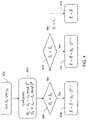
- FIG. 2C illustrates a block diagram of a system 202 for stress compensation using redundancy assisted noise control for accumulated iteration compression error, according to some embodiments of the present disclosure.
- the system 202 includes all the components of FIG. 2A .
- the system 202 also includes an encoder (e.g., a channel encoder) 222 , a first channel decoder 222 , a second channel decoder 242 , and a truncator 234 .
- the encoder 222 encodes the accumulated brightness value (also referred to as “accumulated stress value”) it receives from the adding circuit 220 to protect (e.g., preserve) a portion of the brightness value that is later used to mitigate noise.
- the protected portion of the brightness value may be a k bits (k being an integer greater than 1) near the middle portion of the brightness value, as will be discussed below.
- the encoder 222 may store a duplicate copy of the protected portion in the memory 205 for later use by the first and second channel decoders 232 and 242 .
- the duplicate portion may be stored in an uncompressed form, may be compressed using lossless/lossy compression prior to storing in memory (e.g., by the compressor 235 ), or a coded version of the protected portion may be stored in memory.
- Each of the channel decoders 232 and 242 may utilize the protected portion stored in the memory 205 to reduce the compression noise arising from the compression and decompression operations respectively performed by the compressor 235 and a corresponding one of the decompressors 230 and 240 .
- the compression/decompression error may increase over time and propagate from the lesser significant bit locations to the more significant bit locations.
- the compression/decompression error may increase over time and propagate from the lesser significant bit locations to the more significant bit locations.
- the truncator 234 may discard a portion of the output of the first channel decoder 232 . In some embodiments, the truncator 234 discards the lesser significant bits preceding the protected portion of the brightness value to reduce or minimize accumulated error.
- FIG. 3 illustrates a process for mitigating noise through partial protection of bits by the system 202 , according to some embodiments of the present disclosure.
- the encoder 222 may select k bits of the accumulated brightness value X beginning at the start bit p as the protected portion x k , where both p and k are positive integers greater than one.
- the lesser significant portion x l which is represented by bits from the least significant bit to bit p ⁇ 1, of the accumulated brightness value X may later be discarded by the truncator 234 .
- the values p and k are chosen such that the range of compression/decompression noise is within the protected and lesser significant portions x k and x l , that is, it is limited to the first to (p+k ⁇ 1)-th bits of the accumulated brightness value X.
- the value of p+k ⁇ 1 may be less than a bit length of the accumulated brightness value.
- the length k of the protected portion x k may be 4 to 6, and the value p may be between 6 and 8; however, embodiments of the present disclosure are not limited thereto.
- ignoring the errors that occur in the lesser significant portion x l , protecting the partial information contained in the protected portion x k , and performing error correction using the partial information is sufficient to significantly reduce or to minimize error propagation to the more significant portion x h of the accumulated brightness value X, which is represented by bits from the (p+k)-th bit to the most significant bit.
- the output of the decompressor 230 is represented by the decompressed accumulated brightness value ⁇ tilde over (X) ⁇ (also referred to as “the decompressed value”), and the output of the first channel decoder 232 is represented by the decoded accumulated brightness value ⁇ circumflex over (X) ⁇ (also referred to as “the decoded value”). It is desirable for the decoded value ⁇ circumflex over (X) ⁇ to be as close to the original accumulated brightness value X as possible.
- the decompressed value ⁇ tilde over (X) ⁇ includes the compressed protected portion ⁇ tilde over (x) ⁇ k , the compressed lesser significant portion ⁇ tilde over (x) ⁇ l , and the compressed more significant portion ⁇ tilde over (x) ⁇ h ; and the decoded value ⁇ circumflex over (X) ⁇ includes the decoded protected portion ⁇ circumflex over (x) ⁇ h , the decoded lesser significant portion ⁇ circumflex over (x) ⁇ l , and the decoded more significant portion ⁇ circumflex over (x) ⁇ h .
- N represents the compression noise added to the original value X through the compression and decompression operations performed by the compressor 235 and second decompressor 230 , respectively.
- the first channel decoder 232 estimates the compression noise based on the protected portion x k , which may be maintained intact by the channel encoder and generates an estimated noise ⁇ circumflex over (N) ⁇ .
- the first channel decoder 232 uses the estimated noise ⁇ circumflex over (N) ⁇ to generate the decoded value ⁇ circumflex over (X) ⁇ .
- Equation 2 For this operation to be performed, the values k and p are chosen such that they satisfy the condition of Equation 2 (assuming maximum value of noise N is known, but the sign of N is unknown) or the condition of Equation 3 (assuming both maximum value of noise N and its sign are known): k+p ⁇ 1>log 2 (
- Equation 3 represents the absolute value of the compression noise N.
- Equation 3 is more conservative than the condition Equation 2, as satisfying Equation 3 automatically guarantees satisfying Equation 2.
- N represents the absolute value of the compression noise N.
- Equation 3 is more conservative than the condition Equation 2, as satisfying Equation 3 automatically guarantees satisfying Equation 2.
- Equation 6 the decoded value ⁇ circumflex over (X) ⁇ may satisfy Equation 6:
- the compression noise per iteration is limited to the lesser significant portion x l , which is disregarded.
- FIG. 4 is a flow diagram illustrating the process 400 for mitigating noise by the system 202 , according to some embodiments of the present disclosure.
- the channel decoder 232 / 242 obtains the protected portion x k from the memory 205 and the compressed protected portion ⁇ circumflex over (x) ⁇ k from the second decompressor 230 .
- the channel decoder 232 / 242 calculates the first error value E 1 and the second error value E 2 according to Equations 7 and 8:
- E 1 ( ⁇ tilde over (k) ⁇ k ⁇ x k )mod 2 k (Equation 7)
- E 2 ( x k ⁇ tilde over (x) ⁇ k )mod 2 k (Equation 8)
- the values E 1 and E 2 represent the noise added to the k bits of the protected portion x k .
- the first error E 1 represents a scenario in which the compression noise N has a positive value
- the second error E 2 represents a scenario in which the compression noise N has a negative value.
- Equation 2 it is assumed that only the weaker condition in Equation 2 (and not Equation 3) is satisfied. In such a scenario, there may be the two possible noise values E 1 and E 2 (corresponding to the noise values in Equations 4 and 5) and the channel decoder 232 / 242 determines which one of E 1 or E 2 is the correct noise, which should be compensated.
- the channel decoder 232 / 242 equates the decoded value ⁇ circumflex over (X) ⁇ with the decompressed value ⁇ tilde over (X) ⁇ (i.e., perform no noise mitigation).
- the channel decoder 232 / 242 may instead bias one side or the other by calculating the decoded value ⁇ circumflex over (X) ⁇ according to Equation 9 or 10.
- the first and second errors E 1 and E 2 cannot equal one another.
- Equation 2 is met (and not Equation 3) for some pixels.
- Violating the condition of Equation 3 may result in some miscorrection, but this scheme provides lower value p for the same value k, which may be desirable in that fewer bits are discarded.
- the protected portion x k is maintained intact (i.e., not compressed/decompressed) for purposes of noise mitigation, embodiments of the present disclosure are not limited thereto.
- partial protection may be achieved with multiple replications of the protected portion x k .
- FIG. 5 illustrates a process for mitigating noise through partial protection of bits with multiple replications by the system 202 , according to some embodiments of the present disclosure.
- the channel encoder 222 creates n replicas (n being an integer greater than 1) of the protected portion x k and combines them together to form a binary replica string S.
- the binary replica string S is compressed by compressor 235 and later decompressed by the decompressor 230 .
- the compression and decompression may be the same as those applied to the accumulated brightness value X; however, embodiments of the present disclosure are not limited thereto.
- the compression and decompression applied to the binary replica string S may be different from those applied to the accumulated brightness value X.
- a different compression technique and/or a different compression ratio may be used.
- each of the decompressed replicas (e.g., ⁇ tilde over (x) ⁇ k,2 , ⁇ tilde over (x) ⁇ k,3 , . . . ⁇ tilde over (x) ⁇ k,n+1 ) of the decompressed replica string S experiences a different amount of noise.
- the channel decoder 232 / 242 applies a maximum likelihood decoding process (MLD, e.g., majority vote) to the decompressed replicas to calculate a decoded protected portion ex k , which is an estimation of the protected portion x k of the accumulated brightness value.
- MLD maximum likelihood decoding process
- the MLD process may reduce the noise in decoded protected portion ex k , but may not reduce it down to a point where the decoded protected portion ex k is the same as the protected portion x k .
- the number n of replicas may be determined based on simulations, experimentation, and/or available memory. In some examples, the number of replicas n is chosen to be an odd number.
- the compressed portion ⁇ tilde over (x) ⁇ k,1 may be combined with the binary replica string S to make the total number be an odd number prior to applying the MLD process.
- Embodiments of the present disclosure are not limited to the MLD process, and any other suitable process may be utilized in its place.
- the channel decoder 232 / 242 may proceed to calculate the decoded value ⁇ tilde over (X) ⁇ , as described above with reference to FIG. 4 , by replacing x k with ex k in Equations 7 and 8.
- FIG. 6 illustrates a process for mitigating noise through partial protection of bits with dependent encoding of multiple pixels by enhanced coding techniques, such as reed-solomon code, by the system 202 , according to some embodiments of the present disclosure.
- FIGS. 7A-7D illustrate various placement options for the insertion of parity bits into the corresponding accumulated brightness value, according to some embodiments of the present disclosure.
- the channel encoder 222 may encode the accumulated brightness values X for k′ pixels (k′ being an integer greater than one), whereby these pixels of the display are within one slice of the image being compressed.
- the lesser significant portion x 1 , the protected portion x k , and the more significant portion x h of these pixels are shown as x l,1 . . . x l,k′ , x k,k′ , and x h,1 . . . x h,k′ , respectively.
- the channel encoder 222 then generates parity bits p 1 to P r for the string of bits made up of x k,1 . . . x k,k′ .
- Each of the pixels 1 to k′ and the parity bits p 1 to p r are compressed separately or partly together with the compressor 235 or with multiple different compressors and later decompressed by the corresponding decompressor to generate compressed pixels 1 to k′ and compressed parity bits ⁇ tilde over (p) ⁇ 1 to ⁇ tilde over (p) ⁇ r .
- the parity bits p 1 to p r may be compressed with the same or different compressions (e.g., same or different compression technique, compression ratio, compression parameter, etc.) as the string of bits x k,1 . . . x k,k′ .
- the compressed parity bits ⁇ tilde over (p) ⁇ 1 to ⁇ tilde over (p) ⁇ r are then used by the channel decoder 232 / 242 to generate the values ⁇ circumflex over (x) ⁇ k,1 . . . ⁇ circumflex over (x) ⁇ k,k′ from the ⁇ tilde over (x) ⁇ k,1 . . . ⁇ tilde over (x) ⁇ k,k′ .
- These values are then used by the channel decoder 232 / 242 to estimate the values x k,1 . . . x k,k′ , which can be used to mitigate noise as described above with reference to FIGS. 3-4 .
- the parity bits ⁇ tilde over (p) ⁇ 1 to ⁇ tilde over (p) ⁇ r may be appended/interleaved at any point in the accumulated brightness value.
- the parity bits ⁇ tilde over (p) ⁇ 1 to ⁇ tilde over (p) ⁇ r may be appended to the end of the accumulated brightness value (as, e.g., shown in FIG. 7A ), may be appended to the beginning of the accumulated brightness value (as, e.g., shown in FIG. 7B ), may be appended to somewhere between the LSB and MSB of the accumulated brightness value (as, e.g., shown in FIG. 7C ), or may be interleaved with the bits of the accumulated brightness value (as, e.g., shown in FIG. 7D ).
- the values p and k are fixed and are based on an estimation or knowledge of the noise.
- the noise is not fixed and is accumulated over time.
- the chosen values p and k may be too aggressive at the beginning.
- each of the iterations/runs may correspond to a frame of images displayed at the display device.
- each successive frame may correspond to a successive iteration.
- one iteration may be performed for every m frames (m being an integer greater than 1). The latter approach may reduce the demands on memory and computation time.
- Adaptive parameters allow for easy parameter initialization, as parameters that are inappropriate can be corrected in successive executions. Further, with adaptive parameters may offer better performance at the beginning and therefore allow for less error accumulation during the early runs. Furthermore, no knowledge of the noise is required.
- the accumulated noise starts out small but grows over time (i.e., starts from a least significant bit (LSB) and moves toward a most significant bit (MSB))
- LSB least significant bit
- MSB most significant bit
- p+k also referred to as the sum parameter c
- the value k is kept constant. Therefore the value of p increases over time (e.g., from an LSB toward an MSB).
- FIGS. 8A-8B are diagrams illustrating the maximum absolute error versus number of iterations of the recursive system 202 , according to some example embodiments of the present disclosure.
- FIGS. 8A-8B illustrate the step-like characteristic of the accumulated compression quantization noise.
- FIG. 8B illustrates adaptive noise mitigation using a varying sum parameter c. Further, the appropriate value of the sum parameter c at each step is shown in FIG. 8B . In the example of FIG. 8B , the sum parameter c is increased in increments of one.
- the data accumulation, and hence the noise accumulation may continue for a long period of time (e.g., months or years), and the sum parameter c may be updated at intervals (e.g., regular intervals, such as once every few weeks or months).
- the changes to the sum parameter c may be relatively infrequent.
- this error is diluted by the number of iterations using the correct value of C, and hence there is no discernable effect on the image quality of the display.
- the second approach may be referred to as self-adaptive.
- the compressor 235 may utilize a quantization table (which may be different from the stress profile table maintained in the memory 205 ) and, in some examples, the incrementing of c happens when compression quantization changes (as represented by the step changes in FIG. 8B ). In this case, the compressor 235 signals to the channel encoder and decoder to increment the sum value c whenever the quantization level is changed.
- the quantization levels and their correspondence to c may be based on experiential numbers or theoretical calculations.
- the channel decoder 232 / 242 observes the value of
- the noise threshold may be defined based on the values of p and k and the iteration number (or time).
- the first and second channel decoders 232 and 242 when one of the first and second channel decoders 232 and 242 changes the sum value c, it communicates the change to the other channel decoder so that there is no noise caused by mismatched c.
- the first and second channel decoders 232 and 242 do not communicate the change in the sum value c
- the other decoder may detect the mismatched c by utilizing the same self-adaptive logic leveraging on the additional noise due to mismatched c, and increment the sum value c by one.
- noise mitigation is not performed by the channel encoder 222 and decoders 232 and 242 when the sum value of c is changed.
- the compression block i.e., the compressor 235
- the decision to change c may be made in the same manner as that of the self-adaptive approach.
- first”, “second”, “third”, etc. may be used herein to describe various elements, components, regions, layers and/or sections, these elements, components, regions, layers and/or sections should not be limited by these terms. These terms are only used to distinguish one element, component, region, layer or section from another element, component, region, layer or section. Thus, a first element, component, region, layer or section discussed herein could be termed a second element, component, region, layer or section, without departing from the spirit and scope of the inventive concept.
- a layer when referred to as being “between” two layers, it can be the only layer between the two layers, or one or more intervening layers may also be present.
- the electronic or electric devices and/or any other relevant devices or components according to embodiments of the present disclosure described herein may be implemented utilizing any suitable hardware, firmware (e.g. an application-specific integrated circuit), software, or a combination of software, firmware, and hardware.
- the various components of these devices may be formed on one integrated circuit (IC) chip or on separate IC chips.
- the various components of these devices may be implemented on a flexible printed circuit film, a tape carrier package (TCP), a printed circuit board (PCB), or formed on one substrate.
- the various components of these devices may be a process or thread, running on one or more processors, in one or more computing devices, executing computer program instructions and interacting with other system components for performing the various functionalities described herein.
- the computer program instructions are stored in a memory which may be implemented in a computing device using a standard memory device, such as, for example, a random access memory (RAM).
- the computer program instructions may also be stored in other non-transitory computer readable media such as, for example, a CD-ROM, flash drive, or the like.
- a person of skill in the art should recognize that the functionality of various computing devices may be combined or integrated into a single computing device, or the functionality of a particular computing device may be distributed across one or more other computing devices without departing from the spirit and scope of the exemplary embodiments of the present disclosure.
Landscapes
- Engineering & Computer Science (AREA)
- Physics & Mathematics (AREA)
- Computer Hardware Design (AREA)
- General Physics & Mathematics (AREA)
- Theoretical Computer Science (AREA)
- Control Of Indicators Other Than Cathode Ray Tubes (AREA)
- Control Of El Displays (AREA)
- Compression, Expansion, Code Conversion, And Decoders (AREA)
- Transforming Electric Information Into Light Information (AREA)
Abstract
Description
{tilde over (X)}=X+N (Equation 1)
k+p−1>log2(|N|) (Equation 2)
k+p−2>log2(|N|) (Equation 3)
{circumflex over (N)} 1=({circumflex over (x)} k −x k)×2p−1, or {circumflex over (N)} 2=2p+k−1+({circumflex over (x)} k −x k)×2p−1 (Equation 4)
X+div(N,2(p−1))≠X−div(N,2(p−1))mod 2k (Equation 5)
|{circumflex over (X)}−X|<2p−1 (Equation 6)
E 1=({tilde over (k)} k −x k)mod 2k (Equation 7)
E 2=(x k −{tilde over (x)} k)mod 2k (Equation 8)
{circumflex over (X)}={tilde over (X)}−E 1·2p−1 (Equation 9)
{circumflex over (X)}={tilde over (X)}+E 2·2p−1 (Equation 10)
Claims (19)
E 1=({tilde over (k)} k −x k)mod 2k, and
E 2=(x k −{tilde over (x)} k)mod 2k
{circumflex over (X)}={tilde over (X)}−E 1·2p−1
{circumflex over (X)}={tilde over (X)}−E 2·2p−1
Priority Applications (6)
| Application Number | Priority Date | Filing Date | Title |
|---|---|---|---|
| US16/542,233 US11308873B2 (en) | 2019-05-23 | 2019-08-15 | Redundancy assisted noise control for accumulated iterative compression error |
| KR1020200033961A KR102611866B1 (en) | 2019-05-23 | 2020-03-19 | Method and system of stress compensation in display device |
| EP20169950.1A EP3742430B1 (en) | 2019-05-23 | 2020-04-16 | Method and system of stress compensation in display device |
| TW109115795A TWI833020B (en) | 2019-05-23 | 2020-05-13 | Method and system of stress compensation in display device |
| JP2020085488A JP7393295B2 (en) | 2019-05-23 | 2020-05-14 | Display device stress compensation method and system |
| CN202010447480.1A CN111986619B (en) | 2019-05-23 | 2020-05-25 | Method and system for stress compensation in display device |
Applications Claiming Priority (2)
| Application Number | Priority Date | Filing Date | Title |
|---|---|---|---|
| US201962851872P | 2019-05-23 | 2019-05-23 | |
| US16/542,233 US11308873B2 (en) | 2019-05-23 | 2019-08-15 | Redundancy assisted noise control for accumulated iterative compression error |
Publications (2)
| Publication Number | Publication Date |
|---|---|
| US20200372858A1 US20200372858A1 (en) | 2020-11-26 |
| US11308873B2 true US11308873B2 (en) | 2022-04-19 |
Family
ID=70294953
Family Applications (1)
| Application Number | Title | Priority Date | Filing Date |
|---|---|---|---|
| US16/542,233 Active 2040-01-01 US11308873B2 (en) | 2019-05-23 | 2019-08-15 | Redundancy assisted noise control for accumulated iterative compression error |
Country Status (6)
| Country | Link |
|---|---|
| US (1) | US11308873B2 (en) |
| EP (1) | EP3742430B1 (en) |
| JP (1) | JP7393295B2 (en) |
| KR (1) | KR102611866B1 (en) |
| CN (1) | CN111986619B (en) |
| TW (1) | TWI833020B (en) |
Cited By (1)
| Publication number | Priority date | Publication date | Assignee | Title |
|---|---|---|---|---|
| US20220303133A1 (en) * | 2021-03-19 | 2022-09-22 | Infineon Technologies Ag | Compression in Lattice-Based Cryptography |
Families Citing this family (4)
| Publication number | Priority date | Publication date | Assignee | Title |
|---|---|---|---|---|
| KR102652820B1 (en) * | 2019-12-27 | 2024-04-01 | 엘지디스플레이 주식회사 | Display device and compensation method therefor |
| US11955067B2 (en) | 2021-03-17 | 2024-04-09 | Samsung Display Co., Ltd. | Simplified rate control for an additive iterative compression system |
| US20240379051A1 (en) * | 2021-10-15 | 2024-11-14 | Sharp Kabushiki Kaisha | Display device |
| KR20230089247A (en) * | 2021-12-13 | 2023-06-20 | 엘지디스플레이 주식회사 | Pixel circuit and display device |
Citations (73)
| Publication number | Priority date | Publication date | Assignee | Title |
|---|---|---|---|---|
| US5130786A (en) * | 1989-09-12 | 1992-07-14 | Image Data Corporation | Color image compression processing with compensation |
| US5539468A (en) | 1992-05-14 | 1996-07-23 | Fuji Xerox Co., Ltd. | Coding device and decoding device adaptive to local characteristics of an image signal |
| US6137914A (en) | 1995-11-08 | 2000-10-24 | Storm Software, Inc. | Method and format for storing and selectively retrieving image data |
| US6243416B1 (en) | 1997-03-12 | 2001-06-05 | Oki Data Corporation | Image coding and decoding methods, image coder, and image decoder |
| US20030043088A1 (en) | 2001-08-31 | 2003-03-06 | Booth Lawrence A. | Compensating organic light emitting device displays for color variations |
| US6668086B1 (en) | 1999-05-18 | 2003-12-23 | Canon Kabushiki Kaisha | Tile-based image data decoding method and apparatus |
| US20040061672A1 (en) | 2002-09-27 | 2004-04-01 | Rich Page | Method and apparatus for driving light emitting polymer displays |
| US20040153937A1 (en) * | 2002-11-08 | 2004-08-05 | Lg Electronics Inc. | Video error compensating method and apparatus therefor |
| US6819793B1 (en) | 2000-06-30 | 2004-11-16 | Intel Corporation | Color distribution for texture and image compression |
| US20050225548A1 (en) | 2004-04-09 | 2005-10-13 | Clairvoyante, Inc | System and method for improving sub-pixel rendering of image data in non-striped display systems |
| US20050280766A1 (en) | 2002-09-16 | 2005-12-22 | Koninkiljke Phillips Electronics Nv | Display device |
| US7202912B2 (en) | 2000-05-12 | 2007-04-10 | Thomson Licensing | Method and system for using single OSD pixmap across multiple video raster sizes by chaining OSD headers |
| US7236636B2 (en) | 2003-01-30 | 2007-06-26 | Fujitsu Limited | Image compression method, image restoration method, program and apparatus |
| US20070230572A1 (en) * | 2006-03-28 | 2007-10-04 | Shinichiro Koto | Video decoding method and apparatus |
| US7321693B2 (en) | 2002-11-01 | 2008-01-22 | Ricoh Company, Ltd. | Image processing apparatus and image processing method including adjustment of coded data to specified target size |
| US20080048951A1 (en) | 2006-04-13 | 2008-02-28 | Naugler Walter E Jr | Method and apparatus for managing and uniformly maintaining pixel circuitry in a flat panel display |
| US20080317362A1 (en) | 2007-06-20 | 2008-12-25 | Canon Kabushiki Kaisha | Image encoding apparatus and image decoding apparauts, and control method thereof |
| US20090052772A1 (en) | 2005-02-28 | 2009-02-26 | Nxp B.V. | Compression format and apparatus using the new compression format for temporarily storing image data in a frame memory |
| US20090066613A1 (en) | 2005-10-12 | 2009-03-12 | Canon Kabushiki Kaisha | Display apparatus |
| US20090148059A1 (en) | 2007-12-10 | 2009-06-11 | Sharp Kabushiki Kaisha | Image processing apparatus, image display apparatus, image forming apparatus, image processing method and storage medium |
| US7576888B2 (en) | 2003-07-30 | 2009-08-18 | Seiko Epson Corporation | Color reduction processing apparatus and color reduction method |
| US7619596B2 (en) | 2003-09-09 | 2009-11-17 | Sony Corporation | Image processing apparatus and method of same |
| US7750938B2 (en) | 2002-01-25 | 2010-07-06 | Thomson Licensing | Method and system for maintaining even tube burn-in |
| US20100257493A1 (en) | 2009-04-01 | 2010-10-07 | International Business Machines Corporation | Effective gate length circuit modeling based on concurrent length and mobility analysis |
| US20100316137A1 (en) | 2007-12-03 | 2010-12-16 | Canon Kabushiki Kaisha | For error correction in distributed video coding |
| US20110069076A1 (en) | 2009-09-23 | 2011-03-24 | John Erik Lindholm | Register indexed sampler for texture opcodes |
| US20110148894A1 (en) | 2009-12-21 | 2011-06-23 | Jean-Luc Duprat | Demand-paged textures |
| US7974478B2 (en) | 2006-08-24 | 2011-07-05 | Dell Products L.P. | Methods and apparatus for reducing storage size |
| US20110188750A1 (en) | 2009-09-25 | 2011-08-04 | Canon Kabushiki Kaisha | Image processing apparatus and processing method therefor |
| US20110243469A1 (en) | 2009-10-07 | 2011-10-06 | Mcallister David Kirk | Selecting and representing multiple compression methods |
| US20120120043A1 (en) | 2010-11-16 | 2012-05-17 | Samsung Electronics Co., Ltd. | Image data compressing and decompressing methods and display driving device using the same |
| US20120147799A1 (en) | 2010-12-10 | 2012-06-14 | Sony Corporation | Image processing device, image reproduction device, and image reproduction system |
| US20120320067A1 (en) | 2011-06-17 | 2012-12-20 | Konstantine Iourcha | Real time on-chip texture decompression using shader processors |
| US8452083B2 (en) | 2010-06-09 | 2013-05-28 | Canon Kabushiki Kaisha | Image processing apparatus, image processing method, and computer-readable medium |
| US8478057B1 (en) | 2010-01-22 | 2013-07-02 | Google Inc. | Image compression and decompression using block prediction |
| US20130170558A1 (en) | 2010-09-10 | 2013-07-04 | Thomson Licensing | Video decoding using block-based mixed-resolution data pruning |
| US8509532B2 (en) | 2010-04-28 | 2013-08-13 | Canon Kabushiki Kaisha | Image processing apparatus, image processing method, and computer-readable medium |
| US8533166B1 (en) | 2010-08-20 | 2013-09-10 | Brevity Ventures LLC | Methods and systems for encoding/decoding files and transmission thereof |
| US8553301B2 (en) | 2010-04-08 | 2013-10-08 | Canon Kabushiki Kaisha | Image processing apparatus, method, and program product to perform color-reduction processing for a block |
| US8599925B2 (en) | 2005-08-12 | 2013-12-03 | Microsoft Corporation | Efficient coding and decoding of transform blocks |
| US8659793B2 (en) | 2010-08-26 | 2014-02-25 | Canon Kabushiki Kaisha | Image processing apparatus and image processing method |
| US20140055500A1 (en) | 2012-08-23 | 2014-02-27 | Research In Motion Limited | Organic light emitting diode based display aging monitoring |
| US20140160172A1 (en) | 2012-12-11 | 2014-06-12 | Lg Display Co., Ltd. | Image display device and method for driving the same |
| US20140168192A1 (en) | 2012-12-17 | 2014-06-19 | Lg Display Co., Ltd. | Organic light emitting display device and method for driving the same |
| US20140176409A1 (en) | 2012-12-24 | 2014-06-26 | Lg Display Co., Ltd. | Organic light emitting display device and method of driving the same |
| US20140313360A1 (en) | 2013-04-19 | 2014-10-23 | Samsung Electronics Co., Ltd. | Electronic device and method for operating the same |
| US20150002378A1 (en) | 2005-04-12 | 2015-01-01 | Ignis Innovation Inc. | System and method for compensation of non-uniformities in light emitting device displays |
| US20150015590A1 (en) | 2013-07-15 | 2015-01-15 | Samsung Display Co., Ltd. | Display device, data processing apparatus, and related method |
| US8994617B2 (en) | 2010-03-17 | 2015-03-31 | Ignis Innovation Inc. | Lifetime uniformity parameter extraction methods |
| US8995763B2 (en) | 2012-12-21 | 2015-03-31 | Vmware, Inc. | Systems and methods for determining compression methods to use for an image |
| KR20150034948A (en) | 2013-09-27 | 2015-04-06 | 삼성디스플레이 주식회사 | Organic light emitting display device and method of driving the same |
| US20150117774A1 (en) | 2013-10-30 | 2015-04-30 | Samsung Display Co., Ltd. | Apparatus and method for encoding image data |
| US20150194096A1 (en) | 2014-01-08 | 2015-07-09 | Samsung Display Co., Ltd. | Organic light emitting display device and driving method thereof |
| US20150243201A1 (en) | 2014-02-26 | 2015-08-27 | Samsung Display Co., Ltd. | Organic light emitting display and method for driving the same |
| US20160104411A1 (en) | 2004-12-15 | 2016-04-14 | Ignis Innovation Inc. | Method and system for programming, calibrating and/or compensating, and driving an led display |
| US9495894B2 (en) | 2013-01-21 | 2016-11-15 | Sharp Kabushiki Kaisha | Display device, and data processing method in display device |
| US20160335741A1 (en) | 2014-12-05 | 2016-11-17 | Boe Technology Group Co., Ltd. | Data transfer method, data transfer module, related display panel and method for driving the same, and related display device |
| US20160373788A1 (en) | 2013-07-09 | 2016-12-22 | Sony Corporation | Data encoding and decoding |
| US20160372033A1 (en) | 2015-06-22 | 2016-12-22 | Samsung Display Co., Ltd. | Degradation compensator of organic light emitting diode display device |
| US20160379550A1 (en) | 2015-06-25 | 2016-12-29 | Intel Corporation | Wear compensation for a display |
| US9584696B2 (en) | 2015-03-24 | 2017-02-28 | Semiconductor Components Industries, Llc | Imaging systems with embedded data transmission capabilities |
| US20170122725A1 (en) | 2015-11-04 | 2017-05-04 | Magic Leap, Inc. | Light field display metrology |
| US9715716B2 (en) | 2014-06-26 | 2017-07-25 | Lg Display Co., Ltd. | Data processing apparatus for organic light emitting display device |
| US20170256193A1 (en) | 2015-03-23 | 2017-09-07 | Boe Technology Group Co., Ltd. | Pixel arranging method, pixel rendering method and image display device |
| US20170256024A1 (en) | 2016-03-04 | 2017-09-07 | Samsung Electronics Co., Ltd. | Cache architecture for efficiently accessing texture data using buffers |
| US9812067B2 (en) | 2014-12-15 | 2017-11-07 | Samsung Display Co., Ltd. | Organic light-emitting display device and driving method thereof |
| US9830890B2 (en) | 2015-06-30 | 2017-11-28 | Boe Technology Group Co., Ltd. | Method and device for compressing and decompressing data information, drive compensation method and device, and display device |
| US9894379B2 (en) | 2001-07-10 | 2018-02-13 | The Directv Group, Inc. | System and methodology for video compression |
| US9966035B2 (en) | 2013-12-31 | 2018-05-08 | Lg Display Co., Ltd. | Organic light emitting display device and driving method thereof |
| KR20190060909A (en) | 2017-11-24 | 2019-06-04 | 삼성디스플레이 주식회사 | Organic light emitting display device and method for driving thereof |
| US20190181191A1 (en) | 2017-04-28 | 2019-06-13 | Kunshan Go-Visionox Opto-Electronics Co., Ltd. | Pixel structure driving method |
| US20190289308A1 (en) | 2018-03-15 | 2019-09-19 | Samsung Display Co., Ltd. | Permutation based stress profile compression |
| US10515612B2 (en) | 2018-03-26 | 2019-12-24 | Samsung Display Co., Ltd. | Transformation based stress profile compression |
Family Cites Families (6)
| Publication number | Priority date | Publication date | Assignee | Title |
|---|---|---|---|---|
| US8068544B2 (en) * | 1998-12-21 | 2011-11-29 | Zin Stai Pte. In, Llc | Compression with doppler enhancement |
| JP4398638B2 (en) * | 2002-11-06 | 2010-01-13 | 株式会社東芝 | Video display device and video display method |
| JP2015106096A (en) * | 2013-11-29 | 2015-06-08 | 三星ディスプレイ株式會社Samsung Display Co.,Ltd. | Display device, compensation data calculation method thereof, and driving method thereof |
| JP6744791B2 (en) * | 2015-11-11 | 2020-08-19 | 株式会社Joled | Display device, display device correction method, display device manufacturing method, and display device display method |
| JP6706997B2 (en) * | 2016-08-09 | 2020-06-10 | 株式会社Joled | Display device, display device correction method, display device manufacturing method, and display device display method |
| GB2557997B (en) * | 2016-12-21 | 2019-05-01 | Apical Ltd | Encoding and Decoding of image data |
-
2019
- 2019-08-15 US US16/542,233 patent/US11308873B2/en active Active
-
2020
- 2020-03-19 KR KR1020200033961A patent/KR102611866B1/en active Active
- 2020-04-16 EP EP20169950.1A patent/EP3742430B1/en active Active
- 2020-05-13 TW TW109115795A patent/TWI833020B/en active
- 2020-05-14 JP JP2020085488A patent/JP7393295B2/en active Active
- 2020-05-25 CN CN202010447480.1A patent/CN111986619B/en active Active
Patent Citations (79)
| Publication number | Priority date | Publication date | Assignee | Title |
|---|---|---|---|---|
| US5130786A (en) * | 1989-09-12 | 1992-07-14 | Image Data Corporation | Color image compression processing with compensation |
| US5539468A (en) | 1992-05-14 | 1996-07-23 | Fuji Xerox Co., Ltd. | Coding device and decoding device adaptive to local characteristics of an image signal |
| US6137914A (en) | 1995-11-08 | 2000-10-24 | Storm Software, Inc. | Method and format for storing and selectively retrieving image data |
| US6243416B1 (en) | 1997-03-12 | 2001-06-05 | Oki Data Corporation | Image coding and decoding methods, image coder, and image decoder |
| US6668086B1 (en) | 1999-05-18 | 2003-12-23 | Canon Kabushiki Kaisha | Tile-based image data decoding method and apparatus |
| US7202912B2 (en) | 2000-05-12 | 2007-04-10 | Thomson Licensing | Method and system for using single OSD pixmap across multiple video raster sizes by chaining OSD headers |
| US6819793B1 (en) | 2000-06-30 | 2004-11-16 | Intel Corporation | Color distribution for texture and image compression |
| US9894379B2 (en) | 2001-07-10 | 2018-02-13 | The Directv Group, Inc. | System and methodology for video compression |
| US20030043088A1 (en) | 2001-08-31 | 2003-03-06 | Booth Lawrence A. | Compensating organic light emitting device displays for color variations |
| US7750938B2 (en) | 2002-01-25 | 2010-07-06 | Thomson Licensing | Method and system for maintaining even tube burn-in |
| US20050280766A1 (en) | 2002-09-16 | 2005-12-22 | Koninkiljke Phillips Electronics Nv | Display device |
| US20040061672A1 (en) | 2002-09-27 | 2004-04-01 | Rich Page | Method and apparatus for driving light emitting polymer displays |
| US7321693B2 (en) | 2002-11-01 | 2008-01-22 | Ricoh Company, Ltd. | Image processing apparatus and image processing method including adjustment of coded data to specified target size |
| US20040153937A1 (en) * | 2002-11-08 | 2004-08-05 | Lg Electronics Inc. | Video error compensating method and apparatus therefor |
| US7236636B2 (en) | 2003-01-30 | 2007-06-26 | Fujitsu Limited | Image compression method, image restoration method, program and apparatus |
| US7576888B2 (en) | 2003-07-30 | 2009-08-18 | Seiko Epson Corporation | Color reduction processing apparatus and color reduction method |
| US7619596B2 (en) | 2003-09-09 | 2009-11-17 | Sony Corporation | Image processing apparatus and method of same |
| US20050225548A1 (en) | 2004-04-09 | 2005-10-13 | Clairvoyante, Inc | System and method for improving sub-pixel rendering of image data in non-striped display systems |
| US20160104411A1 (en) | 2004-12-15 | 2016-04-14 | Ignis Innovation Inc. | Method and system for programming, calibrating and/or compensating, and driving an led display |
| US20090052772A1 (en) | 2005-02-28 | 2009-02-26 | Nxp B.V. | Compression format and apparatus using the new compression format for temporarily storing image data in a frame memory |
| US20150002378A1 (en) | 2005-04-12 | 2015-01-01 | Ignis Innovation Inc. | System and method for compensation of non-uniformities in light emitting device displays |
| US8599925B2 (en) | 2005-08-12 | 2013-12-03 | Microsoft Corporation | Efficient coding and decoding of transform blocks |
| US20090066613A1 (en) | 2005-10-12 | 2009-03-12 | Canon Kabushiki Kaisha | Display apparatus |
| US20070230572A1 (en) * | 2006-03-28 | 2007-10-04 | Shinichiro Koto | Video decoding method and apparatus |
| US20080048951A1 (en) | 2006-04-13 | 2008-02-28 | Naugler Walter E Jr | Method and apparatus for managing and uniformly maintaining pixel circuitry in a flat panel display |
| US7974478B2 (en) | 2006-08-24 | 2011-07-05 | Dell Products L.P. | Methods and apparatus for reducing storage size |
| US20080317362A1 (en) | 2007-06-20 | 2008-12-25 | Canon Kabushiki Kaisha | Image encoding apparatus and image decoding apparauts, and control method thereof |
| US20100316137A1 (en) | 2007-12-03 | 2010-12-16 | Canon Kabushiki Kaisha | For error correction in distributed video coding |
| US20090148059A1 (en) | 2007-12-10 | 2009-06-11 | Sharp Kabushiki Kaisha | Image processing apparatus, image display apparatus, image forming apparatus, image processing method and storage medium |
| US20100257493A1 (en) | 2009-04-01 | 2010-10-07 | International Business Machines Corporation | Effective gate length circuit modeling based on concurrent length and mobility analysis |
| US20110069076A1 (en) | 2009-09-23 | 2011-03-24 | John Erik Lindholm | Register indexed sampler for texture opcodes |
| US8660347B2 (en) | 2009-09-25 | 2014-02-25 | Canon Kabushiki Kaisha | Image processing apparatus and processing method therefor |
| US20110188750A1 (en) | 2009-09-25 | 2011-08-04 | Canon Kabushiki Kaisha | Image processing apparatus and processing method therefor |
| US20110243469A1 (en) | 2009-10-07 | 2011-10-06 | Mcallister David Kirk | Selecting and representing multiple compression methods |
| US20110148894A1 (en) | 2009-12-21 | 2011-06-23 | Jean-Luc Duprat | Demand-paged textures |
| US8478057B1 (en) | 2010-01-22 | 2013-07-02 | Google Inc. | Image compression and decompression using block prediction |
| US8994617B2 (en) | 2010-03-17 | 2015-03-31 | Ignis Innovation Inc. | Lifetime uniformity parameter extraction methods |
| US8553301B2 (en) | 2010-04-08 | 2013-10-08 | Canon Kabushiki Kaisha | Image processing apparatus, method, and program product to perform color-reduction processing for a block |
| US8509532B2 (en) | 2010-04-28 | 2013-08-13 | Canon Kabushiki Kaisha | Image processing apparatus, image processing method, and computer-readable medium |
| US8452083B2 (en) | 2010-06-09 | 2013-05-28 | Canon Kabushiki Kaisha | Image processing apparatus, image processing method, and computer-readable medium |
| US8533166B1 (en) | 2010-08-20 | 2013-09-10 | Brevity Ventures LLC | Methods and systems for encoding/decoding files and transmission thereof |
| US8659793B2 (en) | 2010-08-26 | 2014-02-25 | Canon Kabushiki Kaisha | Image processing apparatus and image processing method |
| US20130170558A1 (en) | 2010-09-10 | 2013-07-04 | Thomson Licensing | Video decoding using block-based mixed-resolution data pruning |
| US9071838B2 (en) | 2010-11-16 | 2015-06-30 | Samsung Electronics Co., Ltd. | Image data compressing and decompressing methods and display driving device using the same |
| US20120120043A1 (en) | 2010-11-16 | 2012-05-17 | Samsung Electronics Co., Ltd. | Image data compressing and decompressing methods and display driving device using the same |
| US20120147799A1 (en) | 2010-12-10 | 2012-06-14 | Sony Corporation | Image processing device, image reproduction device, and image reproduction system |
| US9378560B2 (en) | 2011-06-17 | 2016-06-28 | Advanced Micro Devices, Inc. | Real time on-chip texture decompression using shader processors |
| US20120320067A1 (en) | 2011-06-17 | 2012-12-20 | Konstantine Iourcha | Real time on-chip texture decompression using shader processors |
| US20140055500A1 (en) | 2012-08-23 | 2014-02-27 | Research In Motion Limited | Organic light emitting diode based display aging monitoring |
| US20140160172A1 (en) | 2012-12-11 | 2014-06-12 | Lg Display Co., Ltd. | Image display device and method for driving the same |
| US20140168192A1 (en) | 2012-12-17 | 2014-06-19 | Lg Display Co., Ltd. | Organic light emitting display device and method for driving the same |
| US8995763B2 (en) | 2012-12-21 | 2015-03-31 | Vmware, Inc. | Systems and methods for determining compression methods to use for an image |
| US20140176409A1 (en) | 2012-12-24 | 2014-06-26 | Lg Display Co., Ltd. | Organic light emitting display device and method of driving the same |
| US9495894B2 (en) | 2013-01-21 | 2016-11-15 | Sharp Kabushiki Kaisha | Display device, and data processing method in display device |
| US20140313360A1 (en) | 2013-04-19 | 2014-10-23 | Samsung Electronics Co., Ltd. | Electronic device and method for operating the same |
| US20160373788A1 (en) | 2013-07-09 | 2016-12-22 | Sony Corporation | Data encoding and decoding |
| US20150015590A1 (en) | 2013-07-15 | 2015-01-15 | Samsung Display Co., Ltd. | Display device, data processing apparatus, and related method |
| KR20150034948A (en) | 2013-09-27 | 2015-04-06 | 삼성디스플레이 주식회사 | Organic light emitting display device and method of driving the same |
| US20150117774A1 (en) | 2013-10-30 | 2015-04-30 | Samsung Display Co., Ltd. | Apparatus and method for encoding image data |
| US9966035B2 (en) | 2013-12-31 | 2018-05-08 | Lg Display Co., Ltd. | Organic light emitting display device and driving method thereof |
| US20150194096A1 (en) | 2014-01-08 | 2015-07-09 | Samsung Display Co., Ltd. | Organic light emitting display device and driving method thereof |
| US9773455B2 (en) | 2014-01-08 | 2017-09-26 | Samsung Display Co., Ltd. | Organic light emitting display device for compensation of pixel degradation and driving method thereof |
| US20150243201A1 (en) | 2014-02-26 | 2015-08-27 | Samsung Display Co., Ltd. | Organic light emitting display and method for driving the same |
| US9697765B2 (en) | 2014-02-26 | 2017-07-04 | Samsung Display Co., Ltd. | Organic light emitting display and method for driving the same |
| US9715716B2 (en) | 2014-06-26 | 2017-07-25 | Lg Display Co., Ltd. | Data processing apparatus for organic light emitting display device |
| US20160335741A1 (en) | 2014-12-05 | 2016-11-17 | Boe Technology Group Co., Ltd. | Data transfer method, data transfer module, related display panel and method for driving the same, and related display device |
| US9812067B2 (en) | 2014-12-15 | 2017-11-07 | Samsung Display Co., Ltd. | Organic light-emitting display device and driving method thereof |
| US20170256193A1 (en) | 2015-03-23 | 2017-09-07 | Boe Technology Group Co., Ltd. | Pixel arranging method, pixel rendering method and image display device |
| US9584696B2 (en) | 2015-03-24 | 2017-02-28 | Semiconductor Components Industries, Llc | Imaging systems with embedded data transmission capabilities |
| US9905162B2 (en) | 2015-06-22 | 2018-02-27 | Samsung Display Co., Ltd. | Degradation compensator of organic light emitting diode display device |
| US20160372033A1 (en) | 2015-06-22 | 2016-12-22 | Samsung Display Co., Ltd. | Degradation compensator of organic light emitting diode display device |
| US20160379550A1 (en) | 2015-06-25 | 2016-12-29 | Intel Corporation | Wear compensation for a display |
| US9830890B2 (en) | 2015-06-30 | 2017-11-28 | Boe Technology Group Co., Ltd. | Method and device for compressing and decompressing data information, drive compensation method and device, and display device |
| US20170122725A1 (en) | 2015-11-04 | 2017-05-04 | Magic Leap, Inc. | Light field display metrology |
| US20170256024A1 (en) | 2016-03-04 | 2017-09-07 | Samsung Electronics Co., Ltd. | Cache architecture for efficiently accessing texture data using buffers |
| US20190181191A1 (en) | 2017-04-28 | 2019-06-13 | Kunshan Go-Visionox Opto-Electronics Co., Ltd. | Pixel structure driving method |
| KR20190060909A (en) | 2017-11-24 | 2019-06-04 | 삼성디스플레이 주식회사 | Organic light emitting display device and method for driving thereof |
| US20190289308A1 (en) | 2018-03-15 | 2019-09-19 | Samsung Display Co., Ltd. | Permutation based stress profile compression |
| US10515612B2 (en) | 2018-03-26 | 2019-12-24 | Samsung Display Co., Ltd. | Transformation based stress profile compression |
Non-Patent Citations (15)
| Title |
|---|
| "Burrows-Wheeler Transform CMSC 423", 2009, 26 pages. |
| Battail, Gerard, et al., "Decodage par repliques [Replication Coding]," with English Abstract, Annales Des Telecommunications, vol. 31, Nov. 1976, pp. 387-404. |
| Burrows, M., et al., "A Block-sorting Lossless Data Compression Algorithm", SRC Research Report 124, May 10, 1994, 24 pages, d i g i t a l Systems Research Center, Palo Alto, California. |
| Database Compendex [Online], Nov. 1976, Database accession No. EIX77090006481, 1 page. |
| EPO Extended Search Report dated Mar. 6, 2020, for corresponding European Patent Application No. 19191346.6, 8 pages. |
| EPO Extended Search Report dated May 2, 2019, for corresponding European Patent Application No. 19162833.8 (15 pages). |
| EPO Extended Search Report dated Nov. 10, 2020, issued in European Patent Application No. 20195820.4 (10 pages). |
| EPO Extended Search Report dated Nov. 17, 2020, for corresponding European Patent Application No. 20169950.1, (32 pages). |
| Kang, Wei, et al., "Compressing Encrypted Data: A Permutation Approach", Fiftieth Annual Allerton Conference Allerton House, UIUC, Illinois, USA, Oct. 2012 (IEEE), (5 pages). |
| Notice of Allowance issued in U.S. Appl. No. 15/983,014 by the USPTO, dated Aug. 28, 2019, 7 pages. |
| Office Action issued in U.S. Appl. No. 15/980,623 by the USPTO, dated Feb. 4, 2020, 6 pages. |
| Office Action issued in U.S. Appl. No. 16/292,181 by the USPTO, dated Apr. 9, 2020, 7 pages. |
| Partial European Search Report for corresponding European Patent Application No. 20169950.1, dated Aug. 3, 2020, 31 pages. |
| Syahrul, Elfitrin, et al., "Lossless Image Compression Using Burrows Wheeler Transform (Methods And Techniques)", 2008 IEEE International Conference on Signal Image Technology and Internet Based Systems, 2008, pp. 338-343. |
| U.S. Office Action dated Aug. 19, 2021, issued in U.S. Appl. No. 16/657,803 (12 pages). |
Cited By (2)
| Publication number | Priority date | Publication date | Assignee | Title |
|---|---|---|---|---|
| US20220303133A1 (en) * | 2021-03-19 | 2022-09-22 | Infineon Technologies Ag | Compression in Lattice-Based Cryptography |
| US12273454B2 (en) * | 2021-03-19 | 2025-04-08 | Infineon Technologies Ag | Compression in lattice-based cryptography |
Also Published As
| Publication number | Publication date |
|---|---|
| CN111986619A (en) | 2020-11-24 |
| TWI833020B (en) | 2024-02-21 |
| US20200372858A1 (en) | 2020-11-26 |
| EP3742430B1 (en) | 2025-07-23 |
| JP7393295B2 (en) | 2023-12-06 |
| EP3742430A3 (en) | 2020-12-16 |
| TW202113795A (en) | 2021-04-01 |
| KR102611866B1 (en) | 2023-12-11 |
| JP2020191634A (en) | 2020-11-26 |
| KR20200135721A (en) | 2020-12-03 |
| CN111986619B (en) | 2024-12-31 |
| EP3742430A2 (en) | 2020-11-25 |
Similar Documents
| Publication | Publication Date | Title |
|---|---|---|
| US11308873B2 (en) | Redundancy assisted noise control for accumulated iterative compression error | |
| CN110277055B (en) | Method for operating a display, system and display for performing stress compensation | |
| CN112527223B (en) | Method and system for stress compensation in display device | |
| US10803791B2 (en) | Burrows-wheeler based stress profile compression | |
| US20240249674A1 (en) | Simplified rate control for an additive iterative compression system | |
| KR102666533B1 (en) | Display, display driving method, and system of compensating stress on display |
Legal Events
| Date | Code | Title | Description |
|---|---|---|---|
| FEPP | Fee payment procedure |
Free format text: ENTITY STATUS SET TO UNDISCOUNTED (ORIGINAL EVENT CODE: BIG.); ENTITY STATUS OF PATENT OWNER: LARGE ENTITY |
|
| AS | Assignment |
Owner name: SAMSUNG DISPLAY CO., LTD., KOREA, REPUBLIC OF Free format text: ASSIGNMENT OF ASSIGNORS INTEREST;ASSIGNORS:MOBASHER, AMIN;CHEN, ZEHUI;REEL/FRAME:050786/0382 Effective date: 20190815 |
|
| STPP | Information on status: patent application and granting procedure in general |
Free format text: NON FINAL ACTION MAILED |
|
| STPP | Information on status: patent application and granting procedure in general |
Free format text: RESPONSE TO NON-FINAL OFFICE ACTION ENTERED AND FORWARDED TO EXAMINER |
|
| STPP | Information on status: patent application and granting procedure in general |
Free format text: FINAL REJECTION MAILED |
|
| STPP | Information on status: patent application and granting procedure in general |
Free format text: ADVISORY ACTION MAILED |
|
| STCV | Information on status: appeal procedure |
Free format text: NOTICE OF APPEAL FILED |
|
| STPP | Information on status: patent application and granting procedure in general |
Free format text: NOTICE OF ALLOWANCE MAILED -- APPLICATION RECEIVED IN OFFICE OF PUBLICATIONS |
|
| STPP | Information on status: patent application and granting procedure in general |
Free format text: AWAITING TC RESP., ISSUE FEE NOT PAID |
|
| STPP | Information on status: patent application and granting procedure in general |
Free format text: NOTICE OF ALLOWANCE MAILED -- APPLICATION RECEIVED IN OFFICE OF PUBLICATIONS |
|
| STPP | Information on status: patent application and granting procedure in general |
Free format text: PUBLICATIONS -- ISSUE FEE PAYMENT VERIFIED |
|
| STCF | Information on status: patent grant |
Free format text: PATENTED CASE |
|
| MAFP | Maintenance fee payment |
Free format text: PAYMENT OF MAINTENANCE FEE, 4TH YEAR, LARGE ENTITY (ORIGINAL EVENT CODE: M1551); ENTITY STATUS OF PATENT OWNER: LARGE ENTITY Year of fee payment: 4 |