US11306409B2 - Method to enable electroplating of golden silver nanoparticles - Google Patents
Method to enable electroplating of golden silver nanoparticles Download PDFInfo
- Publication number
- US11306409B2 US11306409B2 US16/849,666 US202016849666A US11306409B2 US 11306409 B2 US11306409 B2 US 11306409B2 US 202016849666 A US202016849666 A US 202016849666A US 11306409 B2 US11306409 B2 US 11306409B2
- Authority
- US
- United States
- Prior art keywords
- substrate
- electroplating
- solution
- activated surface
- silver
- Prior art date
- Legal status (The legal status is an assumption and is not a legal conclusion. Google has not performed a legal analysis and makes no representation as to the accuracy of the status listed.)
- Active
Links
Images




Classifications
-
- C—CHEMISTRY; METALLURGY
- C25—ELECTROLYTIC OR ELECTROPHORETIC PROCESSES; APPARATUS THEREFOR
- C25D—PROCESSES FOR THE ELECTROLYTIC OR ELECTROPHORETIC PRODUCTION OF COATINGS; ELECTROFORMING; APPARATUS THEREFOR
- C25D5/00—Electroplating characterised by the process; Pretreatment or after-treatment of workpieces
- C25D5/10—Electroplating with more than one layer of the same or of different metals
- C25D5/12—Electroplating with more than one layer of the same or of different metals at least one layer being of nickel or chromium
-
- C—CHEMISTRY; METALLURGY
- C25—ELECTROLYTIC OR ELECTROPHORETIC PROCESSES; APPARATUS THEREFOR
- C25D—PROCESSES FOR THE ELECTROLYTIC OR ELECTROPHORETIC PRODUCTION OF COATINGS; ELECTROFORMING; APPARATUS THEREFOR
- C25D3/00—Electroplating: Baths therefor
- C25D3/02—Electroplating: Baths therefor from solutions
- C25D3/12—Electroplating: Baths therefor from solutions of nickel or cobalt
-
- C—CHEMISTRY; METALLURGY
- C25—ELECTROLYTIC OR ELECTROPHORETIC PROCESSES; APPARATUS THEREFOR
- C25D—PROCESSES FOR THE ELECTROLYTIC OR ELECTROPHORETIC PRODUCTION OF COATINGS; ELECTROFORMING; APPARATUS THEREFOR
- C25D21/00—Processes for servicing or operating cells for electrolytic coating
- C25D21/12—Process control or regulation
-
- C—CHEMISTRY; METALLURGY
- C25—ELECTROLYTIC OR ELECTROPHORETIC PROCESSES; APPARATUS THEREFOR
- C25D—PROCESSES FOR THE ELECTROLYTIC OR ELECTROPHORETIC PRODUCTION OF COATINGS; ELECTROFORMING; APPARATUS THEREFOR
- C25D3/00—Electroplating: Baths therefor
- C25D3/02—Electroplating: Baths therefor from solutions
- C25D3/38—Electroplating: Baths therefor from solutions of copper
-
- C—CHEMISTRY; METALLURGY
- C25—ELECTROLYTIC OR ELECTROPHORETIC PROCESSES; APPARATUS THEREFOR
- C25D—PROCESSES FOR THE ELECTROLYTIC OR ELECTROPHORETIC PRODUCTION OF COATINGS; ELECTROFORMING; APPARATUS THEREFOR
- C25D3/00—Electroplating: Baths therefor
- C25D3/02—Electroplating: Baths therefor from solutions
- C25D3/48—Electroplating: Baths therefor from solutions of gold
-
- C—CHEMISTRY; METALLURGY
- C25—ELECTROLYTIC OR ELECTROPHORETIC PROCESSES; APPARATUS THEREFOR
- C25D—PROCESSES FOR THE ELECTROLYTIC OR ELECTROPHORETIC PRODUCTION OF COATINGS; ELECTROFORMING; APPARATUS THEREFOR
- C25D5/00—Electroplating characterised by the process; Pretreatment or after-treatment of workpieces
- C25D5/10—Electroplating with more than one layer of the same or of different metals
- C25D5/12—Electroplating with more than one layer of the same or of different metals at least one layer being of nickel or chromium
- C25D5/14—Electroplating with more than one layer of the same or of different metals at least one layer being of nickel or chromium two or more layers being of nickel or chromium, e.g. duplex or triplex layers
-
- C—CHEMISTRY; METALLURGY
- C25—ELECTROLYTIC OR ELECTROPHORETIC PROCESSES; APPARATUS THEREFOR
- C25D—PROCESSES FOR THE ELECTROLYTIC OR ELECTROPHORETIC PRODUCTION OF COATINGS; ELECTROFORMING; APPARATUS THEREFOR
- C25D5/00—Electroplating characterised by the process; Pretreatment or after-treatment of workpieces
- C25D5/18—Electroplating using modulated, pulsed or reversing current
-
- C—CHEMISTRY; METALLURGY
- C25—ELECTROLYTIC OR ELECTROPHORETIC PROCESSES; APPARATUS THEREFOR
- C25D—PROCESSES FOR THE ELECTROLYTIC OR ELECTROPHORETIC PRODUCTION OF COATINGS; ELECTROFORMING; APPARATUS THEREFOR
- C25D5/00—Electroplating characterised by the process; Pretreatment or after-treatment of workpieces
- C25D5/34—Pretreatment of metallic surfaces to be electroplated
-
- C—CHEMISTRY; METALLURGY
- C25—ELECTROLYTIC OR ELECTROPHORETIC PROCESSES; APPARATUS THEREFOR
- C25D—PROCESSES FOR THE ELECTROLYTIC OR ELECTROPHORETIC PRODUCTION OF COATINGS; ELECTROFORMING; APPARATUS THEREFOR
- C25D9/00—Electrolytic coating other than with metals
- C25D9/02—Electrolytic coating other than with metals with organic materials
Definitions
- the present disclosure relates generally to electroplating. More specifically, the present disclosure describes methods to enable electroplating of golden silver nanoparticles.
- “Golden” silver nanoparticles have an atomically precise molecular formula [Ag 25 (SR 18 ] ⁇ (—SR is a thiolate) and is the only silver nanoparticle that has a virtually identical analogue in gold, i.e., [Au 25 (SR) 18 ] ⁇ , in terms of number of metal atoms, ligand count, superatom electronic configuration, and atomic arrangement. Furthermore, both [Ag 25 (SR) 18 ] ⁇ and its gold analogue share a number of features in their optical absorption spectra. In other words, such silver nanoparticles look and behave like gold despite underlying differences between the two elements.
- Gold electroplated electronic components, connectors and integrated circuitry are typically used in electronic equipment, hardware systems and industrial applications such as aerospace, automotive, computers, medical equipment. Such electroplating are often required to adhere electroplating standards set by AMS 2422, ASTM B488, and MIL-G-45204.
- FIG. 1 illustrates steps for a method to enable electroplating of nanomaterial (e.g., on to beryllium copper substrates) according to some embodiments.
- nanomaterial e.g., on to beryllium copper substrates
- FIG. 2 is a cross-sectional scanning electron microscopy (“SEM”) image captured at 3100 ⁇ magnification of a copper substrate electroplated with the nanoparticles using the disclosed method according to some embodiments.
- SEM scanning electron microscopy
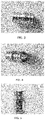
- FIG. 3 depicts a copper push-on connector plated with an alloy according to certain embodiments.
- FIG. 4 depicts a copper push-on connector plated with an alloy according to certain embodiments.
- FIG. 5 depicts a copper push-on connector plated with an alloy according to certain embodiments.
- FIG. 6 depicts illustrates steps for a method to enable electroplating of nanomaterial (e.g., on to a brass and/or a leaded brass alloy) according to certain embodiments.
- FIG. 7 is a cross-sectional SEM image of a brass substrate electroplated with the nanoparticles using the disclosed method according to other embodiments.
- FIG. 8 is a table depicting the concentration of the nanoparticles of Test Samples 1-3 of FIGS. 3, 4, and 5 according to some embodiments.
- FIG. 9 is a graph of an ASTM B117 Neutral Salt Spray (“NSS”) test of a copper substrate plated with 100 microinches of the nanoparticles versus a copper substrate plated with 100 microinches according to certain embodiments.
- FIG. 10 is a table depicting the weight percentages of the elements of Test Samples 1-3 according to other embodiments.
- FIG. 11 is a table depicting X-ray fluorescence thickness measurements of Test Samples 1-3 according to yet still other embodiments.
- FIG. 12 is a graph depicting Knoop hardness measurements (HK25) according to some embodiments.
- FIG. 13 depicts a Pourbaix diagram for the nanoparticles according to some embodiments.
- FIG. 14 illustrates high-resolution SEM images of the nanoparticles between 10-50 nm in diameter obtained using various current densities and pulse signals.
- any embodiment may incorporate only one or a plurality of the above-disclosed aspects of the disclosure and may further incorporate only one or a plurality of the above-disclosed features.
- any embodiment discussed and identified as being “preferred” is considered to be part of a best mode contemplated for carrying out the embodiments of the present disclosure.
- Other embodiments also may be discussed for additional illustrative purposes in providing a full and enabling disclosure.
- many embodiments, such as adaptations, variations, modifications, and equivalent arrangements, will be implicitly disclosed by the embodiments described herein and fall within the scope of the present disclosure.
- any sequence(s) and/or temporal order of steps of various processes or methods that are described herein are illustrative and not restrictive. Accordingly, it should be understood that, although steps of various processes or methods may be shown and described as being in a sequence or temporal order, the steps of any such processes or methods are not limited to being carried out in any particular sequence or order, absent an indication otherwise. Indeed, the steps in such processes or methods generally may be carried out in various different sequences and orders while still falling within the scope of the present disclosure. Accordingly, it is intended that the scope of patent protection is to be defined by the issued claim(s) rather than the description set forth herein.
- the present disclosure includes many aspects and features. Moreover, while many aspects and features relate to, and are described in the context of methods to enable electroplating of golden silver nanoparticles, embodiments of the present disclosure are not limited to use only in this context.
- Golden silver nanoparticles have an atomically precise molecular formula [Ag 25 (SR) 18 ] ⁇ (—SR: thiolate) and single-crystal structure determined.
- This synthesized nanocluster is the only silver nanoparticle that has a virtually identical analogue in gold, i.e., [Au 25 (SR) 18 ] ⁇ , in terms of number of metal atoms, ligand count, superatom electronic configuration, and atomic arrangement.
- both [Ag 25 (SR) 18 ] ⁇ and its gold analogue share a number of features in their optical absorption spectra. In other words, such silver nanoparticles look and behave like gold despite underlying differences between the two elements.
- Plated electronic components such as connectors or integrated circuitry for electronic equipment or other hardware system and industrial applications such as aerospace, automotive, computers, medical equipment, are usually governed by a plurality of standards, which includes, but is not limited to AMS 2422, ASTM B488, MIL-G-45204. Together, the standards may be summarized as follows: a plating thickness of at least 50 ASTM Type III purity level (99.9% golden silver nanoparticles minimum), ASTM Type I (99.7% golden silver nanoparticles minimum).
- the golden silver nanoparticles are silver nanoparticles that possess an atomically precise molecular formula [Ag 25 (SR) 18 ] ⁇ (—SR: thiolate).
- the nanoparticles are preferably silver nanoparticles between 1-100 nm in size.
- the nanoparticles are the only silver nanoparticles that have an virtually identical analogue in gold, i.e., [Au 25 (SR) 18 ] ⁇ , in terms of number of metal atoms, ligand count, super-atom electronic configuration, and atomic arrangement.
- both the nanoparticles and its gold analogue share a number of features in their optical absorption spectra.
- the nanoparticles arguably offer the first model nanoparticle platform to explore the centuries-old problem of understanding the fundamental differences between silver and gold in terms of nobility, catalytic activity, and optical property.
- the nanoparticles share of the same material properties as gold such as: superb low-voltage electrical conductivity, excellent thermal conductivity, high resistance to corrosion (e.g., in this specific atomic configuration the nanoparticles do not tarnish), ductility, excellent solderability, yellow lustrous metal in appearance.
- the nanoparticles have a thermal conductivity of 429 W/mK, an electrical resistivity of 22 ⁇ m, a density of 9.320 g/cm 3 , and a melting point of 961.78° C. (1763.204° F.).
- the instant disclosure seeks to provide methods to enable electroplating of the nanoparticles, which mimic gold appearance and a plurality of its properties.
- the size, shape, and surface morphology play an important role in controlling the chemical, physical, optical, and electronic properties of the nanoparticles.
- the methods disclosed herein use Ag 25 (SR) 18 ⁇ (R ⁇ H, PhMe 2 ) nanoclusters, which are thiolate-protected silver clusters that have a matching analogue in gold.
- Methods disclosed herein use a silver nanomaterial (i.e. the nanoparticles) having the properties and appearance of gold.
- the methods disclosed herein also seek to provide a viable alternative to gold plating processes that are utilized in, for example, the electronics industry as well as the fabrication of connectors and integrated circuitry for electronic equipment and/or other hardware systems.
- novel electroplating system disclosed herein also has cost saving benefits. For example, gold and silver spot price potentially hinder the long term use of such materials for electroplating purposes. Comparatively, the nanoparticles are cost effective and have a lower production cost than current gold coatings and is similar in appearance and performance.
- the methods disclosed herein are preferably utilized to electroplate the nanoparticles onto a variety substrates that include, but are not limited to, GPO connectors and brass pins.
- the method in general, includes an anode, a cathode, an electrolytic solution, a pulse plating current, and a pulse plating method.
- a plurality of electroplating baths may be utilized but should be avoided due to dispositive optoelectronic properties of the final products.
- a non-cyanide acidic silver electroplating bath is utilized, according to preferred embodiments.
- the non-cyanide acidic silver electroplating bath contains a soluble silver salt, a thiosulfate complex, trisodium citrate as a reducing agent.
- the nanoparticles have a molecular of formula [Ag 25 (SR) 18 ] ⁇ where (SR) 18 is a thiolate and R is a (H, PhMe 2 ) cluster. To be sure, the nanoparticles are the only thiolate-protected silver nanocluster that has a matching analogue in gold.
- the electroplating bath also contains sodium hydroxide, sodium nitride, sodium sulfate, nano saccharin, and benzoic acid as a brightener.
- the non-cyanide acidic silver electroplating bath also contains a silver source, silver nitride (AgNO 3 ), at a concentration about 20-60 g/L and preferably 20-45 g/L.
- Applicable thiosulphates include, but are not limited to, alkali metal thiosulphates or ammonium thiosulphate.
- the preferred thiosulphate is sodium thiosulphate.
- the thiosulphate forms a complex with the silver that employs about two moles of thiosulphate for each mole of silver.
- the trisodium citrate is employed as a reducing agent at a concentration of 10-60 g/L grams and preferable 30-50 g/L.
- Sodium hydroxide is subsequently added thereby causing a change in the master mix solution color to light yellow.
- the master mix solution is heated under continuous stirring using a magnetic stirrer at up to about 140° F.
- the term “about” refers to +/ ⁇ 5° F.
- the sodium nitride and sodium sulfate are added to increase electroplating conductivity of the electroplating bath.
- Nano saccharin is added to act as a “grander” to facilitate formation of the nanoparticles with diameters of 30-40 nm and lengths of up to 50 ⁇ m.
- the electroplating bath may be maintained at pH of 3.5-6.5.
- the electroplating bath has a pH of 4.5-5.5.
- the addition of the silver nanoparticles act as a “leaven” to thereby form the nanoparticles.
- the average size of the nanoparticles ranges from 15-500 nm.
- Particle size is preferably controlled by changing the reaction temperature, pH and the electroplating current condition.
- the pulse current has a current density of 45-200 ASF, a pulse frequency of 0-1200 Hz; an on-time of 0.3-3.0 ms, an off-time of 0.5-3.0 ms, and a duty cycle of 10-50%.
- electroplating the nanoparticles onto the surface of substrates includes surface activation of the substrate to promote the adhesion of the metal electrolytic deposition of a thin layer of copper metal and nickel metal for brass pins and a thin layer of nickel metal for beryllium copper GPO connectors, electrolytic deposition of a thin layer of gold strike, and electroplating of the nanoparticle and/or an alloy of the nanoparticles to the substrate surface.
- the nanoparticles may be electroplated on to beryllium copper substrates.
- GPO connectors are typically made of beryllium copper.
- the term “specimen” refers to beryllium copper substrates.
- the surface activation of the specimen preferably includes cleaning/activating of the surface of the substrate to promote metal adhesion via a plurality of first counter flow conditioning rinses.
- the first counter flow conditioning rinses include an acetone rinse followed by an alcohol (e.g., 50% methyl alcohol) rinse. Subsequently, nitrogen gas is used to dry the surface of the substrate.
- the dried surface is cleaned with 15% non-etch type alkaline cleaner (e.g., Isoprep 44®, Vender: MacDermid, Inc.) and activated using an activator solution that includes 20% activator (e.g., Multiprep 506®, Vender: Macdermid, Inc.).
- 15% non-etch type alkaline cleaner e.g., Isoprep 44®, Vender: MacDermid, Inc.
- an activator solution e.g., Multiprep 506®, Vender: Macdermid, Inc.
- the surface of the substrate is rinsed using an ammonia dead rinse solution of 5% ammonium hydroxide and DI water.
- the surface of substrate is conditioned by a plurality of second counter flow conditioning rinses of 5% ammonium hydroxide and DI water.
- the surface of the substrate is etched using a solution of 20% hydrochloric acid.
- a plurality of third counter flow conditioning rinses are used to rinse the surface of the substrate.
- a woods nickel strike material e.g., as provided by Technic, Inc.
- electrolytic nickel e.g., Techni-Nickel HT-2®, Technic, Inc.
- Gold strike e.g., Technic ACR 41®, Technic, Inc
- the electroplating step requires a pH of 3.5-6.5 and a deposition rate of 0.0001 ⁇ m/h.
- FIG. 1 illustrates steps for a method to enable electroplating of nanomaterial (e.g., on beryllium copper substrates) according to some embodiments.
- a surface of a substrate e.g., a beryllium copper substrate
- first counter flow conditioning rinses with a solution of acetone followed by a solution of alcohol.
- Surface activation of the substrate promotes adhesion of the metal.
- the surface of the substrate is rinsed.
- the surface of the substrate is dried using nitrogen gas.
- the surface of the substrate is cleaned using a soak-clean solution that includes 15% non-etch type alkaline cleaner.
- the surface of the substrate is activated using an activator solution that includes 20% activator.
- the surface of the substrate is rinsed using an ammonia dead rinse solution that includes 5% ammonium hydroxide and DI water.
- the surface of substrate is conditioned using a plurality of second counter flow conditioning rinses.
- the surface of the substrate is etched using a solution of 20% hydrochloric acid.
- the surface of the substrate is rinsed using a plurality of third counter flow conditioning rinses.
- surface activation of substrates disclosed in the instant application is accomplished as follows: water is removed from the substrate; the substrate is immersed in acetone; the substrate is immersed in alcohol; the substrate is rinsed; the substrate is deoxidized (e.g., using a laser); the substrate is rinsed; the substrate is deoxidized using sulfuric acid; and the substrate is rinsed.
- FIG. 2 is a cross-sectional scanning electron microscopy (“SEM”) image captured at 3100 ⁇ magnification of a copper substrate electroplated with the nanoparticles using the disclosed method according to some embodiments.
- the SEM image depicts a copper substrate plated with an electrolytic nickel.
- FIGS. 3-5 depict examples of copper push-on connectors (Test Samples 1, 2, and 3) plated with an alloy of the nanoparticles according to some embodiments.
- the nanoparticles may be electroplated onto the surfaces of brass substrates (e.g., brass pins).
- the electroplating of brass substrates, such as brass pins preferably includes the steps of readying the surface of the substrate for the electroplating process, depositing metal onto the surface of the substrate, and electroplating the nanoparticles onto the surface of the substrate.
- Readying the surface of the brass substrate for the electroplating process preferably includes cleaning/activating of the surface of the substrate to promote metallic adhesion using a plurality of first counter flow conditioning rinses that uses a solution acetone followed by a solution of alcohol.
- the cleaned/activated surface is dried using nitrogen gas and conditioned using a desmear solution that includes 15% conditioner (e.g., Ciricuposit 3320®, Dow Chemical, Inc.).
- the conditioned surface of the substrate is rinsed using a deoxidation solution that includes 30% deoxidatant (e.g., a peroxide-based chemical polishing solution such as Laser EX®).
- the substrate surface is further conditioned using a plurality of second counter flow rinses of 5% ammonium hydroxide and DI water, rinsed using a second deoxidation solution that includes 10% deoxidant, preferably sulfuric acid (e.g., Sulfuric Acid 66 Degrees BE′), and rinsed using a plurality of third counter flow conditioning rinses.
- a second deoxidation solution that includes 10% deoxidant, preferably sulfuric acid (e.g., Sulfuric Acid 66 Degrees BE′), and rinsed using a plurality of third counter flow conditioning rinses.
- Depositing metal onto the surface of the substrate preferably includes depositing electrolytic copper, preferably acid copper, and electrolytic nickel (e.g., Techni-Nickel HT-2®, Technic Inc.) followed by the electrodeposition of gold strike (e.g., Technic ACR 41®, Vender: Technic Inc) metal to the surface of the substrate.
- electrolytic copper preferably acid copper
- electrolytic nickel e.g., Techni-Nickel HT-2®, Technic Inc.
- gold strike e.g., Technic ACR 41®, Vender: Technic Inc
- the nanoparticles and/or alloys of the nanoparticles are preferably electroplated onto the surface of the substrate while the pH level of the electroplating solution is 3.5-6.5 and the rate of deposition is about 0.0001 ⁇ m/h.
- FIG. 6 depicts illustrates steps for a method to enable electroplating of nanomaterial according to certain embodiments.
- a surface of a substrate e.g., a brass material or a leaded brass alloy
- first counter flow conditioning rinses with a solution of acetone followed by a solution of alcohol.
- the surface of the substrate is rinsed.
- the surface of the substrate is dried using nitrogen gas.
- the surface of substrate is conditioned using a desmear solution comprising 15% conditioner.
- the surface of the substrate is rinsed using a deoxidation solution comprising 30% deoxidant.
- conditioning of the surface of substrate is conditioned using a plurality of second counter flow rinses.
- the surface of the substrate is rinsed using a second deoxidation solution comprising 10% deoxidant.
- the surface of the substrate is rinsed using a plurality of third counter flow conditioning rinses.
- electrolytic copper and electrolytic nickel metal is deposited on to the surface of the substrate.
- a gold strike metal is electrodeposited on to the surface of the substrate of the substrate.
- nano-silver like gold nanoparticles i.e. the nanoparticles
- an alloy that includes the nano-silver like gold nanoparticles i.e. an alloy of the nanoparticles
- FIG. 7 is a cross-sectional SEM image of a brass substrate electroplated with the nanoparticles using the disclosed method according to other embodiments. The SEM image was captured at 3100 ⁇ and depicts a brass base material (i.e. substrate) plated with copper. A thin layer of nickel is plated on the copper plating and the nanoparticles are plated on the nickel plating.
- the process of the electroplating of the nanoparticles uses an anode, a cathode, an external current, and an electrolyte solution.
- the anode and cathode are immersed in the electrolyte solution and the external current is connected to the anode and cathode.
- the applied voltage is preferably 1-6 V, wherein the external current comprises an anodic-current and a cathodic-current.
- the dissolution of the anode includes platinum and titanium alloy whereby the platinum in the anode acts as a catalyst to accelerate the oxidation process of the nanoparticles.
- Deposition of metallic of the nanoparticle alloys takes place in the cathode.
- When current flows the nano-silver like gold ions are reduced to metallic nano silver like gold nanoparticles on the cathode, for example, brass pins coated with thin layer of copper/nickel metal and of gold strike metal.
- Electroplating of nanoparticles is preferably uses pulse plating methods.
- the preferred pulse plating method utilizes an electrolyte that includes an all salt solution dissolved in 1 L of DI water.
- the electrolyte solution includes silver nitride (20-120 g/L), trisodium citrate (10 g-110 g), sodium hydroxide (5-75 ml/L), the nanoparticles (0.5-10 g/L), sodium nitride (10-100 g/L), sodium sulfate (10-100 g/L), a sodium thiosulfate complex (200-500 g/L), mono saccharin (1-5 g/L), and benzoic acid (1-10 g/L), according to preferred embodiments.
- the electrolyte can include different components, compositions, and/or concentrations than disclosed herein, but ultimately should be discouraged due to suboptimal photoluminescence (i.e. dullness) of the final products.
- Conductivity between the anode (positive charge) and the cathode (negative charge) is provided by a non-cyanide acidic silver electroplating bath that contains a soluble silver salt, a thiosulfate complex, trisodium citrate as a reducing agent.
- the nanoparticles have a molecular formula of [Ag 25 (SR) 18 ] ⁇ where (SR) 18 is a thiolate, (R ⁇ H, PhMe 2 ) nanocluster and is currently the only thiolate-protected silver cluster that has a matching analogue in gold.
- the entire negatively charged, silver-based complex ion has the chemical formula [Ag 25 (SPhMe 2 ) 18 ] ⁇ .
- silver nanoclusters are brown or red in color, but the nanoparticles have the appearance of gold because it reflects light at almost the same wavelength ( ⁇ 675 nm) as gold.
- the virtually identical crystal structures of both nanoclusters allows the nanoparticles to achieve their golden color.
- the electrochemical reaction (electro-deposition) reduction occurs at the cathode where Ag+ nanoparticles are reduced to the nanoparticles and deposited at the cathode.
- the oxidation reaction occurs at the anode to where the complex ion [Ag 25 (SPhMe 2 ) 18 ] ⁇ migrates and oxidizes to Ag 4 O 2 , AgO, or Ag x O and two electrons are produced.
- the preferred pulse plating method is used to obtain crystals characterized by the amorphous structure (nano-structure) of the nanoparticles.
- the pulse plating current includes an on-time and an off-time.
- the nanoparticles are plated out of the electrolyte solution near the cathode interface.
- the cathode diffusion layer is formed until the current is terminated (i.e. off-time) during which the electrolyte solution near the cathode interface becomes replenished with the nanoparticles.
- the diffusion layer is maintained to achieve evenly distributed thickness of deposited nano silver like gold. Such procedure yields improvements in the density across the cathode surface and facilitates uniform deposit thickness.
- re-nucleation typically occurs with each pulse, which thereby increases the number of grains and improves grain reinforcement and nano structure buildup.
- deposition rates are preferably configured to be at least 30 um/h, preferably at least 70 um/h, and more preferably greater than 90 um/h, by passing single or multiple D.C. cathodic-current pulses between the anode and the specimen.
- the cathodic-current pulse frequency is preferably about 0-1200 Hz at pulsed intervals during which the external current on-time period is at least 0.1 ms and preferably about 0.1-100 ms and the off-time is about 0-500 ms.
- the anodic-current pulses has an anodic-time period of 0-100 ms.
- the cathodic duty cycle is 10-50%.
- the on-time may be 0.1-3.0 ms and the off-time 0.2-10.0 ms long.
- the efficiency of pulse electroplating method disclosed herein was tested with the following parameters: an on-time of 0.3-3.0 ms; off-time of 0.5-3.0 ms; and a duty cycle of 10-50%.
- a 40% duty cycle means the power is on 40% of the time and off 60% of the time.
- the nanoparticles typically have a length 6-10,000 nm on average, but superior results are preferably achieved grain sizes less than 1000 nm.
- the thickness of the nanoparticles is time dependent.
- the novel electroplating methods disclosed herein can be optimized by modifying the solution temperature, pH level, and electroplating current conditions. For example, no deposits of the nanoparticle are observed at current densities lower than 10 ASF. When the current density is increased from 45-200 ASF, the Ag x O morphology (grain structure) appears to increase from hundreds of nanometers to several microns.
- FIG. 14 illustrates high-resolution SEM images of the nanoparticles between 10-50 nm in diameter obtained using various current densities and pulse signals.
- FIG. 8 is a table depicting the concentration of the nanoparticles of Test Samples 1-3 of FIGS. 3, 4, and 5 according to some embodiments.
- FIG. 9 is a graph of an ASTM B117 Neutral Salt Spray (“NSS”) test of a copper substrate plated with 100 microinches of the nanoparticles versus a copper substrate plated with 100 microinches according to some embodiments.
- the nanoparticle-plated copper substrate achieved 1000 testing hours in NSS without appearance of corrosion products while the gold-plated copper substrate achieved 1500 testing hours.
- FIG. 10 is a table depicting the weight percentages of the elements of Test Samples 1-3 according to other embodiments.
- FIG. 11 is a table depicting X-ray fluorescence thickness measurements of Test Samples 1-3 according to other embodiments.
- FIG. 12 is a graph depicting Knoop hardness measurements (HK25) according to some embodiments.
- the Knoop graph compares copper substrates plated with soft gold, hard gold, a soft plating of the nanoparticles, and a hard plating of the nanoparticles.
- the data shows that the nanoparticle plating hardness is slightly higher than soft or hard gold hardness.
- the nanoparticle deposit consists of small grain size (nano-size) particles having a hardness 120-200 HK25, which is similar to the hard gold coating.
- the nanoparticle grain size depends on the pulse current plating parameters and electrolyte composition.
- the nanoparticle plating typically achieves a hardness of between 30-90 HK25.
- nickel sulfate hexahydrate e.g. 0.96-3.5 g/L
- FIG. 13 depicts a Pourbaix diagram for the nanoparticles according to some embodiments.
- novel electroplating methods disclosed herein demonstrate that silver can acquire the properties and appearance of gold and can replace gold in gold plating processes known in that art.
- a goal of the instant disclosure is to identify cost effective substitutes for gold in applications where gold nanoparticles are required.
- the novel electroplating methods disclosed herein are applicable in a variety of industries, such as aerospace, automotive, computer, consumer electronics, household appliances, medical equipment, oil & gas equipment, and electronic components (e.g., connectors or integrated circuitry for electronic equipment or other hardware system).
Landscapes
- Chemical & Material Sciences (AREA)
- Engineering & Computer Science (AREA)
- Chemical Kinetics & Catalysis (AREA)
- Electrochemistry (AREA)
- Materials Engineering (AREA)
- Metallurgy (AREA)
- Organic Chemistry (AREA)
- Automation & Control Theory (AREA)
- Electroplating Methods And Accessories (AREA)
- Electroplating And Plating Baths Therefor (AREA)
Abstract
Description
Claims (10)
Priority Applications (1)
| Application Number | Priority Date | Filing Date | Title |
|---|---|---|---|
| US16/849,666 US11306409B2 (en) | 2019-05-23 | 2020-04-15 | Method to enable electroplating of golden silver nanoparticles |
Applications Claiming Priority (2)
| Application Number | Priority Date | Filing Date | Title |
|---|---|---|---|
| US201962852068P | 2019-05-23 | 2019-05-23 | |
| US16/849,666 US11306409B2 (en) | 2019-05-23 | 2020-04-15 | Method to enable electroplating of golden silver nanoparticles |
Publications (2)
| Publication Number | Publication Date |
|---|---|
| US20200370191A1 US20200370191A1 (en) | 2020-11-26 |
| US11306409B2 true US11306409B2 (en) | 2022-04-19 |
Family
ID=73457719
Family Applications (1)
| Application Number | Title | Priority Date | Filing Date |
|---|---|---|---|
| US16/849,666 Active US11306409B2 (en) | 2019-05-23 | 2020-04-15 | Method to enable electroplating of golden silver nanoparticles |
Country Status (1)
| Country | Link |
|---|---|
| US (1) | US11306409B2 (en) |
Families Citing this family (4)
| Publication number | Priority date | Publication date | Assignee | Title |
|---|---|---|---|---|
| KR102295180B1 (en) * | 2021-06-01 | 2021-08-27 | 나상조 | Ag-Nano Alloy Plating Solution Compositions for Improving of Conductivity and Durability and Plating Methods Using Thereof |
| CN113832515A (en) * | 2021-11-09 | 2021-12-24 | 邦仪精密科技(苏州)有限公司 | Metal surface treatment electroplating processing method |
| CN114808034B (en) * | 2022-05-09 | 2024-05-24 | 西安交通大学 | A kind of lamellar flower-shaped nanosilver and its preparation method and application |
| WO2025170607A1 (en) * | 2024-02-06 | 2025-08-14 | Thin Film Service, Inc. | Systems and methods for depositing alternating layers for a diamond-like coating |
Citations (6)
| Publication number | Priority date | Publication date | Assignee | Title |
|---|---|---|---|---|
| US3698880A (en) * | 1969-11-05 | 1972-10-17 | Mallory & Co Inc P R | Solderable stainless steel |
| JP2012067388A (en) | 2010-09-21 | 2012-04-05 | Rohm & Haas Electronic Materials Llc | Method of electroplating silver strike on nickel |
| US9680246B2 (en) | 2013-06-10 | 2017-06-13 | Oriental Electro Plating Corporation | Method for manufacturing plated laminate, and plated laminate |
| US20180265997A1 (en) * | 2017-03-17 | 2018-09-20 | Lawrence Livermore National Security, Llc | Multi-material light-directed electrophoretic deposition and electroplating over large areas using moveable projected images and/or electrodes |
| US20180325429A1 (en) * | 2017-05-12 | 2018-11-15 | The Florida International University Board Of Trustees | Novel method for transdermal measurement of volatile anesthetics |
| US20190271093A1 (en) | 2016-10-24 | 2019-09-05 | Atotech Deutschland Gmbh | A method of depositing a tin layer on a metal substrate and a use of a structure comprising a nickel/phosphorous alloy underlayer and said tin layer with said method |
-
2020
- 2020-04-15 US US16/849,666 patent/US11306409B2/en active Active
Patent Citations (6)
| Publication number | Priority date | Publication date | Assignee | Title |
|---|---|---|---|---|
| US3698880A (en) * | 1969-11-05 | 1972-10-17 | Mallory & Co Inc P R | Solderable stainless steel |
| JP2012067388A (en) | 2010-09-21 | 2012-04-05 | Rohm & Haas Electronic Materials Llc | Method of electroplating silver strike on nickel |
| US9680246B2 (en) | 2013-06-10 | 2017-06-13 | Oriental Electro Plating Corporation | Method for manufacturing plated laminate, and plated laminate |
| US20190271093A1 (en) | 2016-10-24 | 2019-09-05 | Atotech Deutschland Gmbh | A method of depositing a tin layer on a metal substrate and a use of a structure comprising a nickel/phosphorous alloy underlayer and said tin layer with said method |
| US20180265997A1 (en) * | 2017-03-17 | 2018-09-20 | Lawrence Livermore National Security, Llc | Multi-material light-directed electrophoretic deposition and electroplating over large areas using moveable projected images and/or electrodes |
| US20180325429A1 (en) * | 2017-05-12 | 2018-11-15 | The Florida International University Board Of Trustees | Novel method for transdermal measurement of volatile anesthetics |
Non-Patent Citations (3)
| Title |
|---|
| Jin et al., "All-thiolate-protected silver and silver-rich alloy nanoclusters with atomic precision: stable sizes, structural characterization and optical properties", CrystEngComm, 2016, 18, 3996. (Year: 2016). * |
| Lin et al., "The synthesis of Chiral Ag4Pd2(SR)8 by Nonreplaced Galvanic Reaction", Particle & Particle Systems Characterization, 2019, 1900003. (Year: 2019). * |
| Sandmann et al., "Preparation of silver nanoparticles on ITO surfaces by a double-pulse method" J. Electroanalytical Chemistry, 491, 2000, 78-86. (Year: 2000). * |
Also Published As
| Publication number | Publication date |
|---|---|
| US20200370191A1 (en) | 2020-11-26 |
Similar Documents
| Publication | Publication Date | Title |
|---|---|---|
| US20200370191A1 (en) | Method to enable electroplating of golden silver nanoparticles | |
| US5178745A (en) | Acidic palladium strike bath | |
| CN103290457B (en) | The mixture of carbon black and metal | |
| CN101978096B (en) | Ni-p layer system and process for its preparation | |
| TWI287590B (en) | Non-cyanogen type electrolytic solution for plating gold | |
| JPH05271980A (en) | Palladium-nickel alloy plating liquid | |
| EP2873752A1 (en) | Electroless gold plating method and gold-plate-coated material | |
| JP5336762B2 (en) | Copper-zinc alloy electroplating bath and plating method using the same | |
| US11732375B2 (en) | Iron tungsten coating formulations and processes | |
| US6699379B1 (en) | Method for reducing stress in nickel-based alloy plating | |
| TW202028541A (en) | Indium electroplating compositions and methods for electroplating indium on nickel | |
| JP7032502B2 (en) | Acidic Aqueous Silver-Nickel Alloy Electroplating Compositions and Methods | |
| US3684666A (en) | Copper electroplating in a citric acid bath | |
| EP0892087A2 (en) | Electroplating of low-stress nickel | |
| WO2022112379A1 (en) | Ruthenium alloy layer and its layer combinations | |
| CN1896307A (en) | Copper-alloy chemical nickeling process | |
| JP2023553958A (en) | Silver-bismuth electrolyte for the deposition of hard silver layers | |
| JPWO2019098378A1 (en) | Magnesium or aluminum metal member having a black oxide film and its manufacturing method | |
| EP3061851B1 (en) | Method for producing plated article | |
| JPH10130878A (en) | Electrolytic nickel plating method | |
| CN106521574B (en) | A kind of non-cyanide plating solution for copper-plating used and preparation method thereof suitable for width pH and wide current density range | |
| CN1321205A (en) | Aqueous solution for electrodepositing tin-zinc alloys | |
| US10629917B2 (en) | Separator for fuel cells, fuel cell, fuel cell stack, and method of manufacturing separator for fuel cells | |
| JP2560842B2 (en) | Method for manufacturing corrosion resistant film | |
| WO2010101212A1 (en) | Copper-zinc alloy electroplating bath and method of plating using same |
Legal Events
| Date | Code | Title | Description |
|---|---|---|---|
| AS | Assignment |
Owner name: AG-NANO SYSTEM LLC, MICHIGAN Free format text: ASSIGNMENT OF ASSIGNORS INTEREST;ASSIGNOR:PARKER, MARGARET;REEL/FRAME:052407/0573 Effective date: 20200320 |
|
| FEPP | Fee payment procedure |
Free format text: ENTITY STATUS SET TO UNDISCOUNTED (ORIGINAL EVENT CODE: BIG.); ENTITY STATUS OF PATENT OWNER: MICROENTITY |
|
| FEPP | Fee payment procedure |
Free format text: ENTITY STATUS SET TO SMALL (ORIGINAL EVENT CODE: SMAL); ENTITY STATUS OF PATENT OWNER: MICROENTITY Free format text: ENTITY STATUS SET TO MICRO (ORIGINAL EVENT CODE: MICR); ENTITY STATUS OF PATENT OWNER: MICROENTITY |
|
| STPP | Information on status: patent application and granting procedure in general |
Free format text: NON FINAL ACTION MAILED |
|
| STPP | Information on status: patent application and granting procedure in general |
Free format text: FINAL REJECTION MAILED |
|
| STPP | Information on status: patent application and granting procedure in general |
Free format text: DOCKETED NEW CASE - READY FOR EXAMINATION |
|
| STPP | Information on status: patent application and granting procedure in general |
Free format text: NON FINAL ACTION MAILED |
|
| STPP | Information on status: patent application and granting procedure in general |
Free format text: RESPONSE TO NON-FINAL OFFICE ACTION ENTERED AND FORWARDED TO EXAMINER |
|
| STPP | Information on status: patent application and granting procedure in general |
Free format text: FINAL REJECTION MAILED |
|
| STPP | Information on status: patent application and granting procedure in general |
Free format text: DOCKETED NEW CASE - READY FOR EXAMINATION |
|
| STPP | Information on status: patent application and granting procedure in general |
Free format text: NOTICE OF ALLOWANCE MAILED -- APPLICATION RECEIVED IN OFFICE OF PUBLICATIONS |
|
| STPP | Information on status: patent application and granting procedure in general |
Free format text: PUBLICATIONS -- ISSUE FEE PAYMENT RECEIVED |
|
| STPP | Information on status: patent application and granting procedure in general |
Free format text: PUBLICATIONS -- ISSUE FEE PAYMENT VERIFIED |
|
| STCF | Information on status: patent grant |
Free format text: PATENTED CASE |
|
| AS | Assignment |
Owner name: SAMTEC, INC., INDIANA Free format text: ASSIGNMENT OF ASSIGNORS INTEREST;ASSIGNOR:AG-NANO SYSTEM LLC;REEL/FRAME:070596/0653 Effective date: 20250312 |
|
| FEPP | Fee payment procedure |
Free format text: ENTITY STATUS SET TO UNDISCOUNTED (ORIGINAL EVENT CODE: BIG.); ENTITY STATUS OF PATENT OWNER: LARGE ENTITY |
|
| MAFP | Maintenance fee payment |
Free format text: PAYMENT OF MAINTENANCE FEE, 4TH YEAR, LARGE ENTITY (ORIGINAL EVENT CODE: M1551); ENTITY STATUS OF PATENT OWNER: LARGE ENTITY Year of fee payment: 4 |