US11292253B2 - Piezoelectric printing device with inner surface electrode layer - Google Patents
Piezoelectric printing device with inner surface electrode layer Download PDFInfo
- Publication number
- US11292253B2 US11292253B2 US16/912,783 US202016912783A US11292253B2 US 11292253 B2 US11292253 B2 US 11292253B2 US 202016912783 A US202016912783 A US 202016912783A US 11292253 B2 US11292253 B2 US 11292253B2
- Authority
- US
- United States
- Prior art keywords
- ground
- disposed
- printing device
- piezoelectric
- solder joint
- Prior art date
- Legal status (The legal status is an assumption and is not a legal conclusion. Google has not performed a legal analysis and makes no representation as to the accuracy of the status listed.)
- Active, expires
Links
Images


Classifications
-
- B—PERFORMING OPERATIONS; TRANSPORTING
- B41—PRINTING; LINING MACHINES; TYPEWRITERS; STAMPS
- B41J—TYPEWRITERS; SELECTIVE PRINTING MECHANISMS, i.e. MECHANISMS PRINTING OTHERWISE THAN FROM A FORME; CORRECTION OF TYPOGRAPHICAL ERRORS
- B41J2/00—Typewriters or selective printing mechanisms characterised by the printing or marking process for which they are designed
- B41J2/005—Typewriters or selective printing mechanisms characterised by the printing or marking process for which they are designed characterised by bringing liquid or particles selectively into contact with a printing material
- B41J2/01—Ink jet
- B41J2/135—Nozzles
- B41J2/14—Structure thereof only for on-demand ink jet heads
- B41J2/14201—Structure of print heads with piezoelectric elements
- B41J2/14233—Structure of print heads with piezoelectric elements of film type, deformed by bending and disposed on a diaphragm
-
- B—PERFORMING OPERATIONS; TRANSPORTING
- B41—PRINTING; LINING MACHINES; TYPEWRITERS; STAMPS
- B41J—TYPEWRITERS; SELECTIVE PRINTING MECHANISMS, i.e. MECHANISMS PRINTING OTHERWISE THAN FROM A FORME; CORRECTION OF TYPOGRAPHICAL ERRORS
- B41J2/00—Typewriters or selective printing mechanisms characterised by the printing or marking process for which they are designed
- B41J2/005—Typewriters or selective printing mechanisms characterised by the printing or marking process for which they are designed characterised by bringing liquid or particles selectively into contact with a printing material
- B41J2/01—Ink jet
- B41J2/015—Ink jet characterised by the jet generation process
- B41J2/04—Ink jet characterised by the jet generation process generating single droplets or particles on demand
- B41J2/045—Ink jet characterised by the jet generation process generating single droplets or particles on demand by pressure, e.g. electromechanical transducers
- B41J2/04501—Control methods or devices therefor, e.g. driver circuits, control circuits
-
- H01L41/0475—
-
- H—ELECTRICITY
- H10—SEMICONDUCTOR DEVICES; ELECTRIC SOLID-STATE DEVICES NOT OTHERWISE PROVIDED FOR
- H10N—ELECTRIC SOLID-STATE DEVICES NOT OTHERWISE PROVIDED FOR
- H10N30/00—Piezoelectric or electrostrictive devices
- H10N30/20—Piezoelectric or electrostrictive devices with electrical input and mechanical output, e.g. functioning as actuators or vibrators
- H10N30/204—Piezoelectric or electrostrictive devices with electrical input and mechanical output, e.g. functioning as actuators or vibrators using bending displacement, e.g. unimorph, bimorph or multimorph cantilever or membrane benders
- H10N30/2047—Membrane type
-
- H—ELECTRICITY
- H10—SEMICONDUCTOR DEVICES; ELECTRIC SOLID-STATE DEVICES NOT OTHERWISE PROVIDED FOR
- H10N—ELECTRIC SOLID-STATE DEVICES NOT OTHERWISE PROVIDED FOR
- H10N30/00—Piezoelectric or electrostrictive devices
- H10N30/80—Constructional details
- H10N30/87—Electrodes or interconnections, e.g. leads or terminals
- H10N30/875—Further connection or lead arrangements, e.g. flexible wiring boards, terminal pins
-
- B—PERFORMING OPERATIONS; TRANSPORTING
- B41—PRINTING; LINING MACHINES; TYPEWRITERS; STAMPS
- B41J—TYPEWRITERS; SELECTIVE PRINTING MECHANISMS, i.e. MECHANISMS PRINTING OTHERWISE THAN FROM A FORME; CORRECTION OF TYPOGRAPHICAL ERRORS
- B41J2/00—Typewriters or selective printing mechanisms characterised by the printing or marking process for which they are designed
- B41J2/005—Typewriters or selective printing mechanisms characterised by the printing or marking process for which they are designed characterised by bringing liquid or particles selectively into contact with a printing material
- B41J2/01—Ink jet
- B41J2/135—Nozzles
- B41J2/14—Structure thereof only for on-demand ink jet heads
- B41J2002/14403—Structure thereof only for on-demand ink jet heads including a filter
-
- B—PERFORMING OPERATIONS; TRANSPORTING
- B41—PRINTING; LINING MACHINES; TYPEWRITERS; STAMPS
- B41J—TYPEWRITERS; SELECTIVE PRINTING MECHANISMS, i.e. MECHANISMS PRINTING OTHERWISE THAN FROM A FORME; CORRECTION OF TYPOGRAPHICAL ERRORS
- B41J2/00—Typewriters or selective printing mechanisms characterised by the printing or marking process for which they are designed
- B41J2/005—Typewriters or selective printing mechanisms characterised by the printing or marking process for which they are designed characterised by bringing liquid or particles selectively into contact with a printing material
- B41J2/01—Ink jet
- B41J2/135—Nozzles
- B41J2/14—Structure thereof only for on-demand ink jet heads
- B41J2002/14491—Electrical connection
Definitions
- This invention pertains to the field of piezoelectric inkjet printing and more particularly to configurations of a piezoelectric printing device.
- Inkjet printing is typically done by either drop-on-demand or continuous inkjet printing.
- ink drops are ejected onto a recording medium using a drop ejector including a pressurization actuator (thermal or piezoelectric, for example).
- a pressurization actuator thermal or piezoelectric, for example.
- Selective activation of the actuator causes the formation and ejection of a flying ink drop that crosses the space between the printhead and the recording medium and strikes the recording medium.
- the formation of printed images is achieved by controlling the individual formation of ink drops, as is required to create the desired image.
- the desired image can include any pattern of dots directed by image data. It can include graphic or text images. It can also include patterns of dots for printing functional devices or three dimensional structures if appropriate inks are used.
- Ink can include colored ink such as cyan, magenta, yellow or black.
- ink can include conductive material, dielectric material, magnetic material, or semiconductor material for functional printing.
- Ink can include biological, chemical
- Motion of the recording medium relative to the printhead during drop ejection can consist of keeping the printhead stationary and advancing the recording medium past the printhead while the drops are ejected, or alternatively keeping the recording medium stationary and moving the printhead.
- the former architecture is appropriate if the drop ejector array on the printhead can address the entire region of interest across the width of the recording medium.
- Such printheads are sometimes called pagewidth printheads.
- a second type of printer architecture is the carriage printer, where the printhead drop ejector array is somewhat smaller than the extent of the region of interest for printing on the recording medium and the printhead is mounted on a carriage. In a carriage printer, the recording medium is advanced a given distance along a medium advance direction and then stopped.
- the printhead carriage While the recording medium is stopped, the printhead carriage is moved in a carriage scan direction that is substantially perpendicular to the medium advance direction as the drops are ejected from the nozzles.
- the recording medium is advanced; the carriage direction of motion is reversed; and the image is formed swath by swath.
- a drop ejector in a drop-on-demand inkjet printhead includes a pressure chamber having an ink inlet for providing ink to the pressure chamber, and a nozzle for jetting drops out of the chamber.
- a wall of the pressure chamber includes a piezoelectric element that causes the wall to deflect into the ink-filled pressure chamber when a voltage pulse is applied, so that ink is forced through the nozzle.
- Piezoelectric inkjet has significant advantages in terms of chemical compatibility and ejection latitude with a wide range of inks (including aqueous-based inks, solvent-based inks, and ultraviolet-curing inks), as well as the ability to eject different sized drops by modifying the electrical pulse.
- Piezoelectric printing devices also have technical challenges that need to be addressed. Because the amount of piezoelectric displacement per volt is small, the piezoelectric chamber wall area must be much larger than the nozzle area in order to eject useful drop volumes, so that each drop ejector is relatively large. The width of each drop ejector in a row of drop ejectors is limited by the nozzle spacing in that row. As a result, the pressure chambers typically have a length dimension that is much greater than the width dimension. Printing applications that require printing at high resolution and high throughput require large arrays of drop ejectors with nozzles that are closely spaced. Staggered rows of nozzles can provide dots at close spacing on the recording medium through appropriate timing of firing of each row of drop ejectors. However, with many staggered rows, the size of the piezoelectric printing device becomes large.
- a further challenge is that, unlike thermal inkjet printing devices that typically include integrated logic and driving electronics so that the number of leads to the device is reduced, a piezoelectric printing device typically has individual electrical leads for each drop ejector that need to be connected to the driving electronics. In order to apply a voltage across the piezoelectric element independently for each drop ejector in order to eject drops when needed, each drop ejector needs to be associated with two electrodes.
- the two types of electrodes are sometimes called positive and negative electrodes, or individual and common electrodes for example.
- Some types of piezoelectric printing devices are configured such that the two types of electrodes are on opposite surfaces of the piezoelectric element. For making electrical interconnection between the piezoelectric printing device and the driving electronics it can be advantageous to have the two types of electrodes on a same surface of the piezoelectric printing device.
- U.S. Pat. No. 5,255,016 discloses a piezoelectric inkjet printing device in which positive and negative comb-shaped electrodes are formed on an outer surface of a piezoelectric plate.
- the teeth of the comb at least in some regions, extend across the width of the drop ejector.
- a portion of the positive electrode extends along one side edge of the piezoelectric plate, and a portion of the negative electrode extends along an opposite side edge of the piezoelectric plate.
- Individual piezoelectric plates are provided for each drop ejector, resulting in a structure that would be unwieldy to manufacture with large arrays of drop ejectors at tight spacing.
- U.S. Pat. No. 6,243,114 discloses a piezoelectric inkjet printing device in which the common electrode on an outer surface of the piezoelectric plate is comb-shaped with one electrode tooth extending along each side wall of the pressure chamber and a central common electrode tooth extending along the length of the pressure chamber. Two individual electrodes extend along the length of the pressure chamber on opposite sides of the central common electrode tooth.
- U.S. Pat. No. 5,640,184 discloses a piezoelectric inkjet printing device in which pressure chambers for a row of nozzles extend alternately in opposite directions from the row of nozzles.
- a common electrode on a surface of the piezoelectric plate extends along the row of nozzles and has electrode teeth that extend alternately in opposite directions over the side walls of the pressure chambers. Interlaced between the electrode teeth of the common electrode is a spaced array of individual electrodes that are positioned directly over the pressure chambers.
- the piezoelectric plate is mechanically distorted in a shear mode toward the corresponding pressure chamber to cause ejection of an ink drop.
- FIGS. 1 and 2 Chinese Patent Application Publication No. 107344453A discloses a piezoelectric inkjet printing device shown in FIGS. 1 and 2 , which are taken from '453 with some additional labeling added to FIG. 1 for clarification.
- a substrate 100 includes a first side 101 in which a row of pressure chambers 110 is arranged. Each pressure chamber 110 is bounded by side walls 161 and 162 .
- a channel 130 leads from pressure chamber 110 to a nozzle 132 that is disposed on a second side 102 of the substrate 100 .
- the width of the pressure chamber 110 between side walls 161 and 162 is W.
- An ink groove 120 is fluidically connected to an end of each of the pressure chambers 110 in order to provide ink to them.
- a damping structure 140 including a plurality of pillars 141 is provided in each pressure chamber 110 between the ink groove 120 and the channel 130 .
- a driving cover plate 200 includes a piezoelectric plate 210 , made of lead zirconate titinate (PZT) for example.
- a first surface 211 of the piezoelectric plate 210 is bonded to the first side 101 of the substrate 100 .
- An electrode layer 220 is disposed on an outer second surface 212 of the piezoelectric plate 210 .
- the electrode layer 220 includes positive electrodes 221 that are each disposed over the length of the pressure chambers 110 , as well as negative electrodes 222 that are disposed over the length of the side walls 161 and 162 between pressure chambers 110 .
- An ink inlet port 230 is provided through the piezoelectric plate 210 to bring ink from an external ink supply to the ink groove 120 in the substrate 100 .
- Nozzle 132 extends from a flow path 131 in silicon 310 through an oxide layer 320 and a nozzle layer 330 ( FIG. 2 ).
- piezoelectric printing devices having both types of electrodes on an outer surface of a piezoelectric plate away from the pressure chamber have pressure chamber wall displacements that are highly dependent upon the thickness of the piezoelectric plate.
- the integrated displacement of the plate wall can be a factor of ten higher for a plate thickness of 40 microns than for a plate thickness of 100 microns.
- piezoelectric printing devices having both types of electrodes on an inner surface of the piezoelectric plate proximate to the pressure chamber have an integrated displacement of the plate wall that is only 4% higher for a plate thickness of 40 microns than for a plate thickness of 100 microns.
- the displacement for a plate thickness of 40 microns is more than twice as large if the electrodes are on the inner surface of the piezoelectric plate than if they are on the outer surface of the piezoelectric plate.
- drop ejector configurations having the electrodes on the inner surface of the piezoelectric plate can be operated at greater efficiency with lower voltage or smaller chamber dimensions.
- the velocities and volumes of ejected drops are less sensitive to manufacturing variability in piezoelectric plate thickness, resulting in improved print quality.
- What is needed is a configuration of electrodes and electrical lines to facilitate electrical interconnection to the electrodes disposed on the inner surface of the piezoelectric printing device.
- a configuration of rows of drop ejectors on the piezoelectric printing device in a space-efficient manner that can provide ejection of drops for high printing resolution and fast printing throughput.
- a piezoelectric printing device includes a piezoelectric plate and a substrate with an array of at least one row of drop ejectors, such that each row is aligned along a row direction.
- Each drop ejector includes a pressure chamber disposed on a first side of the substrate, the pressure chamber being bounded by a first side wall and a second side wall.
- Each drop ejector also includes a nozzle disposed in a nozzle layer that is formed on a second side of the substrate opposite to the first side.
- the piezoelectric plate has a first surface that is disposed proximate to the first side of the substrate.
- a bonding layer is disposed between the piezoelectric plate and the substrate, the bonding layer having at least one bonding layer window.
- a first electrode layer is disposed on the first surface of the piezoelectric plate.
- the first electrode layer includes a first signal line corresponding to each pressure chamber, each first signal line leading to a corresponding first signal interconnect pad.
- the first electrode layer also includes ground traces disposed on both sides of each pressure chamber, the ground traces being electrically connected to at least one first ground interconnect pad.
- a second electrode layer is disposed on the first side of the substrate.
- the second electrode layer includes a second signal line corresponding to each first signal line.
- Each second signal line leads to a corresponding second signal interconnect pad and a signal input pad, such that the first signal interconnect pad is electrically connected to the second signal interconnect pad through a signal solder joint.
- the second electrode layer also includes a second ground interconnect pad corresponding to each first ground interconnect pad. Each first ground interconnect pad is electrically connected to the corresponding second ground interconnect pad through a ground solder joint.
- the second electrode layer further includes at least one ground return pad that is electrically connected to a plurality of second ground interconnect pads. At least one common ground bus is electrically connected to the at least one ground return pad.
- This invention has the advantage that the electrodes are configured to enable high efficiency of drop ejection with reduced variability of drop volume and drop velocity.
- the electrical lines of the piezoelectric printing device and their corresponding connection pads are configured for compact and reliable electrical interconnection to a printhead package.
- the piezoelectric drop ejectors are configured in a space efficient manner and are capable of high printing resolution and fast printing throughput.
- FIG. 1 shows an exploded perspective view of a prior art piezoelectric drop ejector array configuration
- FIG. 2 shows a cross-section of a single drop ejector of the type shown in FIG. 1 ;
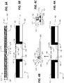
- FIG. 3A shows a cross-section of a portion of a piezoelectric plate
- FIG. 3B shows a cross-section of portion of a substrate corresponding to the portion of the piezoelectric plate shown in FIG. 3A ;
- FIG. 4A is similar to FIG. 3B and indicates an electrode layer on the substrate with an associated solder bump;
- FIGS. 4B and 4C shows magnified views of the electrode layer with the associated solder bump shown in FIG. 4A ;
- FIG. 5 shows the portion of the piezoelectric plate of FIG. 3A mechanically and electrically bonded to the portion of the substrate shown in FIG. 3B ;
- FIG. 6 shows the bonded device of FIG. 5 after removing a portion of the piezoelectric plate in order to expose an interconnect pad region of the electrode layer on the substrate;
- FIG. 7A shows a top view of three drop ejectors in a substrate
- FIG. 7B shows a view of electrical lines on an inner surface of the piezoelectric plate and on the surface of the substrate corresponding to the drop ejectors shown in FIG. 4A ;
- FIG. 8A shows a top view of electrical lines from FIG. 7B on the inner surface of the piezoelectric plate
- FIG. 8B shows a top view of electrical lines from FIG. 7B on the surface of the substrate
- FIG. 9 shows a top view of a single drop ejector and some of its corresponding electrical lines
- FIG. 10 shows a portion of a piezoelectric printing device according to an embodiment
- FIG. 11 shows a masking layer with windows
- FIG. 12 shows a portion of a piezoelectric printing device according to another embodiment.
- FIGS. 13A through 13C show various configurations of the bonding layer window, the insulator window and the solder joint cross-section.
- Words such as “over”, “under”, “above” or “below” are intended to describe positional relationships of features that are in different planes, but it is understood that a feature of a device that is “above” another feature of the device in one orientation would be “below” that feature if the device is turned upside down.
- Piezoelectric printing devices have signal lines and ground traces disposed in a first electrode layer on an inner surface of the piezoelectric plate proximate to the pressure chamber.
- a second electrode layer is disposed on an adjacent surface of the substrate to which the piezoelectric plate is bonded.
- the signal lines and ground traces in the first electrode layer are connected to signal input pads and at least one ground return pad in the second electrode layer through solder joints. The signal input pads and the at least one ground return pad are exposed for connecting the assembled piezoelectric printing device.
- FIG. 3A shows a cross-section of a piezoelectric plate 210 through dashed line 3 - 3 ( FIG. 10 ).
- FIG. 3B shows a cross-section of a corresponding portion of a substrate 100 .
- Piezoelectric plate 210 has a thickness T.
- Substrate 100 includes a pair of pressure chambers 111 and 112 , which extend outwardly from a central region. Each pressure chamber 111 and 112 includes a channel 130 that leads to a nozzle 132 disposed in a nozzle layer 330 .
- Inner first surface 211 of the piezoelectric plate 210 includes grooves 215 to facilitate subsequent removal of a portion of the piezoelectric plate 210 , as described below with reference to FIG.
- First signal lines 251 (part of a first electrode layer 240 ) on inner first surface 211 of the piezoelectric plate 210 extend over pressure chambers 111 and 112 in the assembled device.
- a patterned bonding layer 270 is disposed over the first signal lines 251 and other portions of first surface 211 of the piezoelectric plate 210 .
- Bonding layer 270 includes bonding layer windows 275 .
- the bonding layer 270 can be a polymer adhesive, for example. Bonding layer 270 is disposed between the piezoelectric plate 210 and the substrate 100 and joins piezoelectric plate 210 to the first side 101 of substrate 100 as shown in FIG. 5 .
- bonding layer 270 isolates the ink in pressure chambers 111 and 112 from the electrical lines and the piezoelectric plate 210 .
- an additional insulating layer (not shown) can be added between the bonding layer 270 and the piezoelectric plate 210 , or between the bonding layer 270 and the first side 101 of the substrate 100 for improved reliability.
- the additional insulation layer can be silicon oxide or silicon nitride, for example.
- a second electrode layer 440 is disposed on first surface 101 of the substrate 100 .
- Second electrode layer 440 includes a plurality of second signal lines 451 as well as a common ground bus 464 .
- First electrode layer 240 and second electrode layer 440 can each include a copper layer and can each include at least one chrome layer.
- solder bumps 470 are disposed on the second signal lines 451 in the second electrode layer 440 for connection to the first signal lines 251 in the first electrode layer 240 on the first surface 211 of the piezoelectric plate 210 ( FIG. 3A ).
- FIG. 4A is similar to FIG. 3B and includes a dashed ellipse 105 to indicate a region that is shown at higher magnification in FIG. 4B and at still higher magnification in FIG. 4C .
- An insulating layer 410 such as SiO2 is formed and patterned on second signal line 451 to include an insulator window 412 .
- Insulating layer 410 includes an outer surface 411 that is not in contact with second signal line 451 .
- a second signal interconnect pad 453 corresponds to a portion of second signal line 451 that is exposed within insulator window 412 .
- a A solder bump 470 which includes indium tin alloy solder 471 for example, connects to second signal interconnect pad 453 .
- a base 473 of solder bump 470 is disposed over the insulating layer window 410 and makes contact with second signal interconnect pad 453 through insulator window 412 .
- base 473 can be made of a material, such as copper or copper and chrome, which does not change shape during the bonding process.
- a cap 472 such as a layer of gold, is disposed over the solder 471 .
- the insulating layer 410 is disposed over the second electrode layer 440 on the first side 101 of the substrate 100 .
- Insulating layer 410 has an insulating window 412 corresponding to each second signal interconnect pad 453 and also an insulating window 412 corresponding to each second ground interconnect pad 463 ( FIG. 8B ).
- signal solder joints 475 are formed over the insulator windows 412 between second signal lines 451 (at second signal interconnect pads 453 ) in the second electrode layer 440 and first signal lines 251 (at first signal interconnect pads 253 ) in the first electrode layer 240 .
- ground solder joints 485 FIG. 7B
- solder bumps 470 can be formed on the first electrode layer 240 on the first surface 211 of the piezoelectric plate 210 .
- insulating layer 410 is disposed over the first electrode layer 240 with insulator windows 412 corresponding to each first signal interconnect pad 253 and each first ground interconnect pad 263 ( FIG. 8A ).
- the solder bumps 470 for signal solder joints 475 and the ground solder joints 485 are disposed over the insulator windows 412 in the insulating layer 410 .
- FIG. 5 shows the piezoelectric plate 210 of FIG. 3A bonded to the substrate 100 of FIG. 3B .
- the solder 471 in solder bumps 470 flows to form signal solder joints 475 between second signal lines 451 (at second signal interconnect pads 453 ) and first signal lines 251 (at first signal interconnect pads 253 ).
- Bonding layer 270 which can include materials such as polyimide, SU-8 epoxy and benzocyclobutene-based polymer, provides a structural joint between piezoelectric plate 210 and substrate 100 .
- Solder joints 475 are isolated within bonding layer windows 275 in bonding layer 270 so that they are not exposed to the ink in pressure chambers 111 and 112 .
- the piezoelectric plate 210 is bonded to the substrate 100 , it is diced or etched along cut lines 216 to intersect with grooves 215 ( FIG. 5 ) so that a portion of piezoelectric plate 210 is removed, thereby forming an opening 218 which provides access to portions of second electrode layer 440 , including second signal lines 451 and signal input pads 455 as shown in FIG. 6 .
- FIG. 7A shows a top view of a row of three drop ejectors 150 formed on a substrate 100 ( FIG. 3B ) each drop ejector 150 including a pressure chamber 110 and a nozzle 132 .
- Nozzles 132 (as well as drop ejectors 150 ) are aligned along a row direction 51 and the centers of adjacent nozzles are spaced at a pitch p.
- the nozzle 132 is disposed near a first end 115 of the pressure chamber 110 .
- ink enters the pressure chamber 110 from ink groove 120 (connected to an ink inlet port 230 as in FIGS. 1 and 2 ), through ink inlet 121 , through filter 146 and through restrictor 145 near second end 116 of pressure chamber 110 opposite the first end 115 .
- Ink groove 120 provides ink to a plurality of pressure chambers 110 .
- ink enters ink inlets 121 directly from an edge of the substrate 100 .
- Filter 146 can include pillars similar to the pillars 141 shown in prior art FIG. 1 .
- Restrictor 145 provides flow impedance (as does filter 146 ) to help limit the flow of ink toward inlet 121 when a drop of ink is being ejected from pressure chamber 110 , thereby directing more of the pressure of the deflecting piezoelectric plate to propelling the drop of ink.
- FIG. 7B shows a top view of electrical lines corresponding to the drop ejectors 150 shown in FIG. 7A .
- First signal lines 251 and ground traces 261 are provided as part of first electrode layer 240 disposed on inner first surface 211 piezoelectric plate 210 ( FIG. 3A ). Widths and spacings of first signal lines 251 and ground traces 261 are configured for efficient driving of the piezoelectric plate 210 .
- First signal lines 251 are electrically connected to second signal lines 451 in second electrode layer 440 on first side 101 of substrate 100 ( FIG. 3B ) by signal solder joints 475 ( FIGS. 5 and 6 ).
- Signal input pads 455 are disposed on second signal lines 451 .
- Ground traces 261 are electrically connected to ground leads 461 in second electrode layer 440 on first side 101 of substrate 100 ( FIG. 3B ) by ground solder joints 485 , which are similar to the signal solder joints 475 described above, although they can have different cross-sectional areas and shapes.
- FIG. 8A shows the portions of first electrode layer 240 on inner first surface 211 of piezoelectric plate 210 ( FIG. 3A ) corresponding to FIG. 7B .
- FIG. 8B shows the portions of second electrode layer 440 on first side 101 of substrate 100 ( FIG. 3B ) corresponding to FIG. 7B .
- First signal interconnect pads 253 ( FIG. 8A ) are electrically connected to second signal interconnect pads 453 ( FIG. 8B ) through signal solder joints 475 ( FIG. 7B ).
- Second signal interconnect pads 453 are connected to corresponding second signal lines 451 and signal input pads 455 .
- First ground interconnect pads 263 FIG. 8A
- second ground interconnect pads 463 are electrically connected to second ground interconnect pads 463 ( FIG. 8B ) through ground solder joints 485 ( FIG. 7B ).
- FIG. 9 shows a top view of a single drop ejector 150 (dashed lines) that is disposed in a substrate 100 below the corresponding first signal lines 251 and ground traces 261 disposed on the piezoelectric plate 210 .
- a first signal line 251 is disposed over each corresponding pressure chamber 110 and extends in a direction 52 that is perpendicular to the row direction 51 .
- first signal line 251 is disposed over a center of the corresponding pressure chamber 110 .
- Each first signal line 251 is electrically connected to a corresponding second signal input line 451 and signal input pad 455 on substrate 100 ( FIG. 6 ) through signal solder joint 475 .
- Nozzle 132 is disposed near a first end 115 of the pressure chamber 110 proximate to the signal solder joint 475 .
- First signal line 251 has a width b ( FIG. 7B ) that is greater than 0.1 times the width W ( FIG. 7A ) of the pressure chamber 110 .
- First signal line width b is also greater than 0.2 times the thickness T of the piezoelectric plate 210 ( FIG. 3A ).
- Ground traces 261 are aligned over the first side wall 161 and the second side wall 162 . Ground traces 261 are typically disposed midway between corresponding pressure chambers 110 and extend in a direction 52 that is perpendicular to row direction 51 .
- Ground trace 261 has a width c ( FIG.
- a distance d ( FIG. 7B ) between a first signal line 251 and an adjacent ground trace 261 is typically greater than 0.1 W ( FIG. 7A ).
- a distance d between a first signal line 251 and an adjacent ground trace 261 is typically greater than 0.5 T and less than 2 T ( FIG. 3A ).
- FIG. 10 shows a top view of a portion of a piezoelectric printing device 11 according to an embodiment of the invention.
- a pair of staggered rows 181 and 182 of drop ejectors 150 (similar to those described above with reference to FIGS. 3A through 9 ) is disposed on the substrate 100 . Each row is aligned along row direction 51 .
- First row 181 and second row 182 are spaced apart from each other along a first direction 52 that is perpendicular to row direction 51 .
- Each drop ejector 150 in first row 181 includes a pressure chamber 111 and each drop ejector 150 in second row 182 includes a pressure chamber 112 .
- the pressure chambers 111 and 112 are disposed on a first side 101 of the substrate 100 .
- ink is fed into the ink inlets 121 of each drop ejector 150 directly from the edges of substrate 100 that extend along row direction 51 .
- the pressure chambers 111 and 112 are each bounded by a first side wall 161 and a second side wall 162 .
- Each drop ejector also includes a nozzle 132 that is in fluidic communication with the corresponding pressure chamber 111 or 112 .
- the nozzles 132 are disposed in a nozzle layer 330 on a second side 102 of the substrate 100 .
- a first electrode layer 240 disposed on an inner first surface 211 of a piezoelectric plate 210 includes a first signal line 251 corresponding to each drop ejector 150 in each of the staggered rows 181 and 182 of drop ejectors 150 .
- Each first signal line 251 leads to a corresponding signal input pad 455 that is disposed in second electrode layer 440 on substrate 100 through a signal solder joint 475 and a second signal line 451 .
- the second electrode layer 440 also includes at least one common ground bus 464 that is connected to ground traces 261 in first electrode layer 240 through ground leads 461 on second electrode layer 440 and ground solder joints 485 . Ground traces 261 are aligned over the first and second side walls 161 and 162 of each pressure chamber.
- the common ground bus 464 extends along the row direction 51 and leads to a ground return pad 465 .
- the common ground bus 464 is disposed between the signal input pads 455 of the first staggered row 181 of drop ejectors 150 and the signal input pads 455 of the second staggered row 182 of drop ejectors 150 .
- the signal input pads 455 of the first staggered row 181 of drop ejectors and the signal input pads 455 of the second staggered row 182 of drop ejectors are disposed between the nozzles 132 of the first staggered row 181 of drop ejectors and the nozzles 132 of the second staggered row 182 of drop ejectors.
- All signal input pads 455 and ground return pad(s) 465 are exposed through opening 218 ( FIG. 6 ) in piezoelectric plate 210 .
- Such a configuration of signal input pads 455 and ground return pad(s) 465 is advantageous for providing electrical interconnection from piezoelectric printing device 11 in a compact region to a printhead package (not shown).
- the nozzles 132 in row 181 are spaced at pitch p, and the nozzles 132 in row 182 are also spaced at pitch p.
- the two rows are offset by a distance p/2 along the row direction 51 .
- a recording medium (not shown) is moved relative to piezoelectric printing device 11 along first direction 52 , ejecting ink drops by the drop ejectors in row 181 at a suitable timing relative to ejecting ink drops by the drop ejectors in row 182 can print a composite row of dots on the recording medium with a dot spacing of p/2.
- It is preferable to have a small printing region on the piezoelectric printing device 11 i.e.
- the drop ejectors 150 in rows 182 are oppositely oriented, such that the nozzles 132 of the first staggered row 181 are proximate to the nozzles 132 of the second row, and such that the pressure chambers 111 of the first row 181 and the pressure chambers 112 of the second row 182 extend in opposite directions along first direction 52 from their respective nozzles 132 .
- the printing region can be further reduced on the piezoelectric printing device 11 in the embodiment shown below in FIG. 12 .
- an electrically insulating masking layer 280 can be disposed over the second electrode layer 440 , such that the masking layer 280 includes windows 281 over the signal input pads 455 and a window 282 over the ground return pad 465 in order to expose the pads for electrical interconnection.
- piezoelectric printing device 11 includes a substrate 100 , an array of at least one row 181 of drop ejectors 150 , a piezoelectric plate 210 , a bonding layer 270 , a first electrode layer 240 , a second electrode layer 440 , and at least one common ground bus 464 .
- Each row 181 and 182 of drop ejectors 150 is aligned along a row direction 51 .
- Each drop ejector 150 includes a pressure chamber 110 / 111 / 112 disposed on a first side 101 of the substrate 100 .
- the pressure chamber is bounded by a first side wall 161 and a second side wall 162 .
- Each drop ejector 150 also includes a nozzle 132 disposed in a nozzle layer 330 that is disposed on a second side 102 of the substrate 100 opposite to the first side 101 .
- the piezoelectric plate 210 has a first surface 211 that is proximate to the first side 101 of the substrate 100 .
- Bonding layer 270 is disposed between the piezoelectric plate 210 and the substrate 100 and has bonding layer windows 275 .
- First electrode layer 240 is disposed on the first surface 211 of the piezoelectric plate.
- First electrode layer 240 includes a first signal line 251 corresponding to each pressure chamber 110 / 111 / 112 . Each first signal line 251 leads to a corresponding first signal interconnect pad 253 .
- First electrode layer 240 also includes ground traces 261 that are disposed on both sides of each pressure chamber 110 / 111 / 112 . Ground traces 261 are electrically connected to at least one first ground interconnect pad 263 .
- Second electrode layer 440 is disposed on the first side 101 of the substrate 100 . Second electrode layer 440 includes a second signal line 451 corresponding to each first signal line 251 . Each second signal line 451 leads to a corresponding second signal interconnect pad 453 and a signal input pad 455 . The first signal interconnect pad 253 is electrically connected to the second signal interconnect pad 453 through a signal solder joint 475 . Second electrode layer 440 also includes a second ground interconnect pad 463 .
- Second electrode layer 440 further includes at least one ground return pad 465 that is electrically connected to a plurality of second ground interconnect pads 463 .
- the at least one ground return pad 465 is electrically connected to the at least one common ground bus 464 .
- the at least one common ground bus 464 is disposed in the second electrode layer 440 on the first side 101 of the substrate 100 .
- the array of drop ejectors 150 includes at least two staggered rows 181 and 182 of drop ejectors 150 that are disposed on a common substrate 100 , such that each row 181 and 182 is aligned along the row direction 51 and spaced apart from other rows 181 and 182 along a direction 52 that is perpendicular to the row direction 51 . Additionally, in the FIG.
- the array includes at least one pair of staggered rows 181 and 182 of drop ejectors 150 , where at least one ground bus 464 is disposed between the pair of staggered rows 181 and 182 .
- the nozzles 132 of a first staggered row 181 are proximate to the nozzles 132 of a second staggered row 182 , while the pressure chambers 111 of the first staggered row 181 and the pressure chambers 112 of the second staggered row 182 extend in opposite directions from the respective nozzles 132 .
- FIG. 12 shows a top view of a portion of a piezoelectric printing device 11 according to another embodiment of the invention.
- the configuration shown in FIG. 12 is similar to that shown in FIG. 10 , except the common ground bus 264 is disposed on the first electrode layer 240 and is configured differently.
- a first common ground bus 264 is disposed proximate to the second end 116 of the corresponding pressure chambers 111 in first row 181
- a second common ground bus 266 is disposed proximate to the second end 116 of the corresponding pressure chambers 112 in second row 182 .
- Signal solder joints 475 connect first signal lines 251 with second signal lines 451 and signal input pads 455 and are disposed proximate to the first ends 115 of the pressure chambers 111 and 112 in both rows 181 and 182 , as they were in the FIG. 10 embodiment.
- First common ground bus 264 in first electrode layer 240 is connected to a ground return pad 465 in second electrode layer 440 by ground solder joints 485 .
- Second common ground bus 266 in first electrode layer 240 is connected to a ground return pad 467 in second electrode layer 440 by ground solder joints 486 .
- a similar masking pattern 280 shown in FIG. 11 can be used for exposing the signal input pads and ground return pads for electrical interconnection.
- the drop ejectors 150 and electrical lines described above with reference to FIGS. 3-10 and 12 are well suited for a piezoelectric plate 210 that is configured to cause local deflection of the piezoelectric plate 210 into one or more pressure chambers 110 / 111 / 112 when a voltage pulse is applied to the electrodes corresponding to those pressure chambers 110 / 111 / 112 in order to eject a drop of ink.
- the piezoelectric plate 210 is poled along a direction that is normal to first surface 211 .
- T For efficient deflection of the piezoelectric plate of thickness T into a pressure chamber 110 / 111 / 112 having a width W, it is advantageous for T to be less than 0.5 W, and in some embodiments for T to be less than 0.3 W.
- the pitch p in each row is 0.01 inch, so that the nozzles 132 in each row are disposed at 100 nozzles per inch and a composite row of dots can be printed at 200 dots per inch by the pair of rows.
- a chamber width W can be 224 microns and a side wall width s can be 30 microns, so that s is less than 0.2p as described above with reference to FIG. 7A .
- width b of first signal line 251 is 90 microns
- width c of ground trace 261 is 90 microns
- distance d is 37 microns.
- the width b of first signal line 251 is greater than 0.1 W.
- solder bumps 470 and the resulting solder joints 475 and 485 can be formed over insulator windows 412 in the insulating layer 410 on the first electrode layer 240 or the second electrode layer 440 .
- relative sizes of the solder joints and the corresponding insulator windows and bonding layer windows, as well as the cross-sectional shape of the solder joints can facilitate successful electrical connection between lines in the first electrode layer 240 and the second electrical layer 440 , mechanical bonding between the piezoelectric plate 210 and the substrate 100 , and fluidic isolation of the solder joints from ink in the pressure chambers.
- FIGS. 13A, 13B and 13C show top views of different examples.
- pad 290 can be a first signal interconnect pad 253 , a second signal interconnect pad 453 , a first ground interconnect pad 263 or a second ground interconnect pad 463 for example.
- bonding layer window 275 is shown as a square opening and insulator window 412 is shown as a circular opening, but other shapes are possible.
- the cross-section of the solder joint 475 is noncircular. In the example shown in FIG. 13A , the cross-section of solder joint 475 is elliptical. In the example shown in FIG. 13B , the cross-section of solder joint 475 is triangular. In the example shown in FIG.
- the cross-section of solder joint 475 is shaped like a cross.
- the solder joint 475 cross-section is shown as being polygonal.
- the solder portion 471 of solder bump 470 FIG. 4C
- the solder joint 475 will include rounded corners due to flow of the solder 471 .
- the base 473 is made of a material such as copper or copper and chrome
- the base 473 of solder joint 475 will retain its original shape after bonding.
- a cross-section of a solder joint is understood to include the cross-section of the base 473 .
- FIG. 13C shows an example of a solder joint cross-section having a concave portion. In other words, a portion of the perimeter of the solder joint cross-section extends inward toward the center.
- Non-circular shapes, polygonal shapes and concave shapes of the solder joint 475 facilitate the simultaneous mechanical bonding of the bonding layer 270 and the formation of the solder joint 475 due to surface tension forces in the flowing solder 471 .
- the area of the corresponding insulator window 412 is smaller than the area of the area of the solder joint 475 at the outer surface 411 ( FIGS. 4B and 4C ) of the insulating layer 410 .
- the perimeter of the corresponding insulator window 412 is disposed inside the perimeter of the solder joint 475 at the outer surface 411 of the insulating layer 410 where base 473 is disposed. In other words, a portion of solder bump 470 and the resulting solder joint 475 is disposed on top of the outer surface 411 of the insulating layer 410 .
- the area of the corresponding bonding layer window 275 is larger than the cross-sectional area of the solder joint 475 at the outer surface 411 of the insulating layer 410 . Also, the perimeter of the corresponding bonding layer window 275 is disposed outside the perimeter of the solder joint 475 at the outer surface 411 of the insulating layer 410 . In other words, bonding layer 270 does not touch the solder joint 475 .
Landscapes
- Particle Formation And Scattering Control In Inkjet Printers (AREA)
Abstract
Description
Claims (28)
Applications Claiming Priority (2)
| Application Number | Priority Date | Filing Date | Title |
|---|---|---|---|
| CN202010386134.7 | 2020-05-13 | ||
| CN202010386134.7A CN111923600B (en) | 2020-05-13 | 2020-05-13 | Piezoelectric ink jet printing device with internal surface electrode layer |
Publications (2)
| Publication Number | Publication Date |
|---|---|
| US20210354465A1 US20210354465A1 (en) | 2021-11-18 |
| US11292253B2 true US11292253B2 (en) | 2022-04-05 |
Family
ID=73317510
Family Applications (1)
| Application Number | Title | Priority Date | Filing Date |
|---|---|---|---|
| US16/912,783 Active 2040-08-25 US11292253B2 (en) | 2020-05-13 | 2020-06-26 | Piezoelectric printing device with inner surface electrode layer |
Country Status (2)
| Country | Link |
|---|---|
| US (1) | US11292253B2 (en) |
| CN (1) | CN111923600B (en) |
Citations (8)
| Publication number | Priority date | Publication date | Assignee | Title |
|---|---|---|---|---|
| US5255016A (en) | 1989-09-05 | 1993-10-19 | Seiko Epson Corporation | Ink jet printer recording head |
| US5640184A (en) | 1994-03-21 | 1997-06-17 | Spectra, Inc. | Orifice plate for simplified ink jet head |
| US6243114B1 (en) | 1997-11-27 | 2001-06-05 | Fujitsu Limited | Ink jet head providing improved printing resolution and printing speed |
| US20030098632A1 (en) * | 2001-09-12 | 2003-05-29 | Ngk Insulators, Ltd. | Matrix type piezoelectric/electrostrictive device and manufacturing method thereof |
| WO2013085543A1 (en) * | 2011-12-09 | 2013-06-13 | Hewlett Packard Development Company, L.P. | Printhead waveform voltage amplifier |
| US20150367644A1 (en) * | 2014-06-18 | 2015-12-24 | Seiko Epson Corporation | Liquid ejecting head and manufacturing method of liquid ejecting head |
| US20170056995A1 (en) * | 2015-08-24 | 2017-03-02 | Seagate Technology Llc | Method of forming electrical connections with solder dispensing and reflow |
| CN107344453A (en) | 2016-05-06 | 2017-11-14 | 中国科学院苏州纳米技术与纳米仿生研究所 | A kind of piezoelectric ink jet printing equipment and preparation method thereof |
Family Cites Families (10)
| Publication number | Priority date | Publication date | Assignee | Title |
|---|---|---|---|---|
| JP3991952B2 (en) * | 2003-08-11 | 2007-10-17 | ブラザー工業株式会社 | Inkjet head |
| JP4218594B2 (en) * | 2004-06-08 | 2009-02-04 | ブラザー工業株式会社 | Inkjet head |
| JP4915381B2 (en) * | 2007-09-29 | 2012-04-11 | ブラザー工業株式会社 | Droplet discharge device and droplet discharge head |
| JP2009208234A (en) * | 2008-02-29 | 2009-09-17 | Fuji Xerox Co Ltd | Wiring substrate, liquid droplet delivering head, liquid droplet delivering apparatus, and method for manufacturing wiring substrate |
| JP6168281B2 (en) * | 2013-03-13 | 2017-07-26 | セイコーエプソン株式会社 | Liquid ejecting head, liquid ejecting apparatus, and method of manufacturing liquid ejecting head |
| JP6565253B2 (en) * | 2015-03-24 | 2019-08-28 | セイコーエプソン株式会社 | Head unit and liquid ejection device |
| CN107399166B (en) * | 2016-05-18 | 2019-05-17 | 中国科学院苏州纳米技术与纳米仿生研究所 | A kind of MEMS shearing piezoelectric inkjet print head and preparation method thereof |
| US10532567B2 (en) * | 2017-02-07 | 2020-01-14 | Canon Kabushiki Kaisha | Piezoelectric actuator, method for manufacturing same, and liquid discharge head |
| JP7041547B2 (en) * | 2018-02-20 | 2022-03-24 | 東芝テック株式会社 | Inkjet head, inkjet printer, manufacturing method of inkjet head |
| JP2019162734A (en) * | 2018-03-19 | 2019-09-26 | セイコーエプソン株式会社 | Liquid discharge head, liquid discharge device, piezoelectric device |
-
2020
- 2020-05-13 CN CN202010386134.7A patent/CN111923600B/en active Active
- 2020-06-26 US US16/912,783 patent/US11292253B2/en active Active
Patent Citations (8)
| Publication number | Priority date | Publication date | Assignee | Title |
|---|---|---|---|---|
| US5255016A (en) | 1989-09-05 | 1993-10-19 | Seiko Epson Corporation | Ink jet printer recording head |
| US5640184A (en) | 1994-03-21 | 1997-06-17 | Spectra, Inc. | Orifice plate for simplified ink jet head |
| US6243114B1 (en) | 1997-11-27 | 2001-06-05 | Fujitsu Limited | Ink jet head providing improved printing resolution and printing speed |
| US20030098632A1 (en) * | 2001-09-12 | 2003-05-29 | Ngk Insulators, Ltd. | Matrix type piezoelectric/electrostrictive device and manufacturing method thereof |
| WO2013085543A1 (en) * | 2011-12-09 | 2013-06-13 | Hewlett Packard Development Company, L.P. | Printhead waveform voltage amplifier |
| US20150367644A1 (en) * | 2014-06-18 | 2015-12-24 | Seiko Epson Corporation | Liquid ejecting head and manufacturing method of liquid ejecting head |
| US20170056995A1 (en) * | 2015-08-24 | 2017-03-02 | Seagate Technology Llc | Method of forming electrical connections with solder dispensing and reflow |
| CN107344453A (en) | 2016-05-06 | 2017-11-14 | 中国科学院苏州纳米技术与纳米仿生研究所 | A kind of piezoelectric ink jet printing equipment and preparation method thereof |
Also Published As
| Publication number | Publication date |
|---|---|
| CN111923600B (en) | 2021-10-22 |
| CN111923600A (en) | 2020-11-13 |
| US20210354465A1 (en) | 2021-11-18 |
Similar Documents
| Publication | Publication Date | Title |
|---|---|---|
| EP3909775B1 (en) | Piezoelectric printing device with vias through piezoelectric plate | |
| JP2006123550A (en) | NOZZLE PLATE, INKJET PRINT HEAD HAVING THE SAME, AND METHOD FOR PRODUCING NOZZLE PLATE | |
| CN212267015U (en) | Piezoelectric inkjet printing device with outer surface electrode layer | |
| US11192365B1 (en) | Piezoelectric printhead and printing system | |
| US11198295B2 (en) | Piezoelectric printing device with outer surface electrode layer | |
| CN212267013U (en) | Piezoelectric Inkjet Printing Devices with Through Holes in Piezoelectric Plates | |
| US8434844B2 (en) | Stationary inkjet printhead with dead nozzle compensation provided by nozzles in same nozzles row | |
| US8485623B2 (en) | Pagewidth inkjet printhead configured such that printed dot density exceeds nozzle density | |
| CN212499505U (en) | Piezoelectric inkjet print head and printing system with multiple inks | |
| US11292253B2 (en) | Piezoelectric printing device with inner surface electrode layer | |
| US8714677B2 (en) | Inkjet printhead with join regions seamlessly compensated by directional nozzles | |
| US11285721B2 (en) | Piezoelectric printing device with single layer inner electrode | |
| US11413866B2 (en) | Piezoelectric printhead for multiple inks and printing system | |
| CN212499506U (en) | Piezoelectric inkjet print head and printing system | |
| US8353577B2 (en) | Method of controlling drop directionality from inkjet nozzle using multiple independently-actuable roof paddles | |
| US8506052B2 (en) | Inkjet nozzle assembly with drop directionality control via independently actuable roof paddles | |
| JP2000218803A (en) | Multi-array type multi-color nozzle array print head | |
| US8356884B2 (en) | Printhead integrated circuit having common conductive track fused to nozzle plate | |
| US8540344B2 (en) | Pagewidth inkjet printhead with drop directionality control | |
| US8529005B2 (en) | Method of compensating for dead nozzles in stationary pagewidth printhead | |
| US20120081472A1 (en) | Printhead integrated circuit with end nozzles firing at multiple dot positions | |
| JP2017030192A (en) | Liquid discharge head | |
| JP2002292870A (en) | Inkjet recording head |
Legal Events
| Date | Code | Title | Description |
|---|---|---|---|
| FEPP | Fee payment procedure |
Free format text: ENTITY STATUS SET TO UNDISCOUNTED (ORIGINAL EVENT CODE: BIG.); ENTITY STATUS OF PATENT OWNER: SMALL ENTITY |
|
| FEPP | Fee payment procedure |
Free format text: ENTITY STATUS SET TO SMALL (ORIGINAL EVENT CODE: SMAL); ENTITY STATUS OF PATENT OWNER: SMALL ENTITY |
|
| AS | Assignment |
Owner name: SUZHOU RUIFA PRINTING TECHNOLOGY CO., LTD, CHINA Free format text: ASSIGNMENT OF ASSIGNORS INTEREST;ASSIGNORS:XIE, YONGLIN;ZHANG, XIAOFEI;LV, HUIQIANG;AND OTHERS;SIGNING DATES FROM 20210913 TO 20210916;REEL/FRAME:057522/0320 |
|
| STPP | Information on status: patent application and granting procedure in general |
Free format text: RESPONSE TO NON-FINAL OFFICE ACTION ENTERED AND FORWARDED TO EXAMINER |
|
| STPP | Information on status: patent application and granting procedure in general |
Free format text: NOTICE OF ALLOWANCE MAILED -- APPLICATION RECEIVED IN OFFICE OF PUBLICATIONS |
|
| STPP | Information on status: patent application and granting procedure in general |
Free format text: PUBLICATIONS -- ISSUE FEE PAYMENT VERIFIED |
|
| STCF | Information on status: patent grant |
Free format text: PATENTED CASE |
|
| MAFP | Maintenance fee payment |
Free format text: PAYMENT OF MAINTENANCE FEE, 4TH YR, SMALL ENTITY (ORIGINAL EVENT CODE: M2551); ENTITY STATUS OF PATENT OWNER: SMALL ENTITY Year of fee payment: 4 |