US11290013B2 - Integrated circuit apparatus including regulator circuits - Google Patents
Integrated circuit apparatus including regulator circuits Download PDFInfo
- Publication number
- US11290013B2 US11290013B2 US16/931,829 US202016931829A US11290013B2 US 11290013 B2 US11290013 B2 US 11290013B2 US 202016931829 A US202016931829 A US 202016931829A US 11290013 B2 US11290013 B2 US 11290013B2
- Authority
- US
- United States
- Prior art keywords
- circuit
- regulator circuit
- state
- regulator
- voltage
- Prior art date
- Legal status (The legal status is an assumption and is not a legal conclusion. Google has not performed a legal analysis and makes no representation as to the accuracy of the status listed.)
- Active, expires
Links
Images


Classifications
-
- G—PHYSICS
- G05—CONTROLLING; REGULATING
- G05F—SYSTEMS FOR REGULATING ELECTRIC OR MAGNETIC VARIABLES
- G05F1/00—Automatic systems in which deviations of an electric quantity from one or more predetermined values are detected at the output of the system and fed back to a device within the system to restore the detected quantity to its predetermined value or values, i.e. retroactive systems
- G05F1/10—Regulating voltage or current
- G05F1/46—Regulating voltage or current wherein the variable actually regulated by the final control device is DC
- G05F1/56—Regulating voltage or current wherein the variable actually regulated by the final control device is DC using semiconductor devices in series with the load as final control devices
- G05F1/565—Regulating voltage or current wherein the variable actually regulated by the final control device is DC using semiconductor devices in series with the load as final control devices sensing a condition of the system or its load in addition to means responsive to deviations in the output of the system, e.g. current, voltage, power factor
-
- H—ELECTRICITY
- H02—GENERATION; CONVERSION OR DISTRIBUTION OF ELECTRIC POWER
- H02M—APPARATUS FOR CONVERSION BETWEEN AC AND AC, BETWEEN AC AND DC, OR BETWEEN DC AND DC, AND FOR USE WITH MAINS OR SIMILAR POWER SUPPLY SYSTEMS; CONVERSION OF DC OR AC INPUT POWER INTO SURGE OUTPUT POWER; CONTROL OR REGULATION THEREOF
- H02M3/00—Conversion of DC power input into DC power output
- H02M3/02—Conversion of DC power input into DC power output without intermediate conversion into AC
- H02M3/04—Conversion of DC power input into DC power output without intermediate conversion into AC by static converters
- H02M3/10—Conversion of DC power input into DC power output without intermediate conversion into AC by static converters using discharge tubes with control electrode or semiconductor devices with control electrode
- H02M3/145—Conversion of DC power input into DC power output without intermediate conversion into AC by static converters using discharge tubes with control electrode or semiconductor devices with control electrode using devices of a triode or transistor type requiring continuous application of a control signal
- H02M3/155—Conversion of DC power input into DC power output without intermediate conversion into AC by static converters using discharge tubes with control electrode or semiconductor devices with control electrode using devices of a triode or transistor type requiring continuous application of a control signal using semiconductor devices only
- H02M3/156—Conversion of DC power input into DC power output without intermediate conversion into AC by static converters using discharge tubes with control electrode or semiconductor devices with control electrode using devices of a triode or transistor type requiring continuous application of a control signal using semiconductor devices only with automatic control of output voltage or current, e.g. switching regulators
- H02M3/158—Conversion of DC power input into DC power output without intermediate conversion into AC by static converters using discharge tubes with control electrode or semiconductor devices with control electrode using devices of a triode or transistor type requiring continuous application of a control signal using semiconductor devices only with automatic control of output voltage or current, e.g. switching regulators including plural semiconductor devices as final control devices for a single load
-
- G—PHYSICS
- G05—CONTROLLING; REGULATING
- G05F—SYSTEMS FOR REGULATING ELECTRIC OR MAGNETIC VARIABLES
- G05F1/00—Automatic systems in which deviations of an electric quantity from one or more predetermined values are detected at the output of the system and fed back to a device within the system to restore the detected quantity to its predetermined value or values, i.e. retroactive systems
- G05F1/10—Regulating voltage or current
- G05F1/46—Regulating voltage or current wherein the variable actually regulated by the final control device is DC
- G05F1/56—Regulating voltage or current wherein the variable actually regulated by the final control device is DC using semiconductor devices in series with the load as final control devices
- G05F1/563—Regulating voltage or current wherein the variable actually regulated by the final control device is DC using semiconductor devices in series with the load as final control devices including two stages of regulation at least one of which is output level responsive, e.g. coarse and fine regulation
-
- G—PHYSICS
- G05—CONTROLLING; REGULATING
- G05F—SYSTEMS FOR REGULATING ELECTRIC OR MAGNETIC VARIABLES
- G05F1/00—Automatic systems in which deviations of an electric quantity from one or more predetermined values are detected at the output of the system and fed back to a device within the system to restore the detected quantity to its predetermined value or values, i.e. retroactive systems
- G05F1/10—Regulating voltage or current
- G05F1/46—Regulating voltage or current wherein the variable actually regulated by the final control device is DC
- G05F1/56—Regulating voltage or current wherein the variable actually regulated by the final control device is DC using semiconductor devices in series with the load as final control devices
- G05F1/59—Regulating voltage or current wherein the variable actually regulated by the final control device is DC using semiconductor devices in series with the load as final control devices including plural semiconductor devices as final control devices for a single load
-
- H—ELECTRICITY
- H02—GENERATION; CONVERSION OR DISTRIBUTION OF ELECTRIC POWER
- H02M—APPARATUS FOR CONVERSION BETWEEN AC AND AC, BETWEEN AC AND DC, OR BETWEEN DC AND DC, AND FOR USE WITH MAINS OR SIMILAR POWER SUPPLY SYSTEMS; CONVERSION OF DC OR AC INPUT POWER INTO SURGE OUTPUT POWER; CONTROL OR REGULATION THEREOF
- H02M1/00—Details of apparatus for conversion
- H02M1/08—Circuits specially adapted for the generation of control voltages for semiconductor devices incorporated in static converters
-
- G—PHYSICS
- G01—MEASURING; TESTING
- G01N—INVESTIGATING OR ANALYSING MATERIALS BY DETERMINING THEIR CHEMICAL OR PHYSICAL PROPERTIES
- G01N27/00—Investigating or analysing materials by the use of electric, electrochemical, or magnetic means
- G01N27/02—Investigating or analysing materials by the use of electric, electrochemical, or magnetic means by investigating impedance
- G01N27/22—Investigating or analysing materials by the use of electric, electrochemical, or magnetic means by investigating impedance by investigating capacitance
- G01N27/223—Investigating or analysing materials by the use of electric, electrochemical, or magnetic means by investigating impedance by investigating capacitance for determining moisture content, e.g. humidity
-
- H—ELECTRICITY
- H02—GENERATION; CONVERSION OR DISTRIBUTION OF ELECTRIC POWER
- H02M—APPARATUS FOR CONVERSION BETWEEN AC AND AC, BETWEEN AC AND DC, OR BETWEEN DC AND DC, AND FOR USE WITH MAINS OR SIMILAR POWER SUPPLY SYSTEMS; CONVERSION OF DC OR AC INPUT POWER INTO SURGE OUTPUT POWER; CONTROL OR REGULATION THEREOF
- H02M1/00—Details of apparatus for conversion
- H02M1/0003—Details of control, feedback or regulation circuits
- H02M1/0006—Arrangements for supplying an adequate voltage to the control circuit of converters
-
- H—ELECTRICITY
- H02—GENERATION; CONVERSION OR DISTRIBUTION OF ELECTRIC POWER
- H02M—APPARATUS FOR CONVERSION BETWEEN AC AND AC, BETWEEN AC AND DC, OR BETWEEN DC AND DC, AND FOR USE WITH MAINS OR SIMILAR POWER SUPPLY SYSTEMS; CONVERSION OF DC OR AC INPUT POWER INTO SURGE OUTPUT POWER; CONTROL OR REGULATION THEREOF
- H02M1/00—Details of apparatus for conversion
- H02M1/0003—Details of control, feedback or regulation circuits
- H02M1/0032—Control circuits allowing low power mode operation, e.g. in standby mode
-
- H—ELECTRICITY
- H02—GENERATION; CONVERSION OR DISTRIBUTION OF ELECTRIC POWER
- H02M—APPARATUS FOR CONVERSION BETWEEN AC AND AC, BETWEEN AC AND DC, OR BETWEEN DC AND DC, AND FOR USE WITH MAINS OR SIMILAR POWER SUPPLY SYSTEMS; CONVERSION OF DC OR AC INPUT POWER INTO SURGE OUTPUT POWER; CONTROL OR REGULATION THEREOF
- H02M1/00—Details of apparatus for conversion
- H02M1/0003—Details of control, feedback or regulation circuits
- H02M1/0038—Circuits or arrangements for suppressing, e.g. by masking incorrect turn-on or turn-off signals, e.g. due to current spikes in current mode control
-
- H—ELECTRICITY
- H02—GENERATION; CONVERSION OR DISTRIBUTION OF ELECTRIC POWER
- H02M—APPARATUS FOR CONVERSION BETWEEN AC AND AC, BETWEEN AC AND DC, OR BETWEEN DC AND DC, AND FOR USE WITH MAINS OR SIMILAR POWER SUPPLY SYSTEMS; CONVERSION OF DC OR AC INPUT POWER INTO SURGE OUTPUT POWER; CONTROL OR REGULATION THEREOF
- H02M1/00—Details of apparatus for conversion
- H02M1/0048—Circuits or arrangements for reducing losses
-
- Y—GENERAL TAGGING OF NEW TECHNOLOGICAL DEVELOPMENTS; GENERAL TAGGING OF CROSS-SECTIONAL TECHNOLOGIES SPANNING OVER SEVERAL SECTIONS OF THE IPC; TECHNICAL SUBJECTS COVERED BY FORMER USPC CROSS-REFERENCE ART COLLECTIONS [XRACs] AND DIGESTS
- Y02—TECHNOLOGIES OR APPLICATIONS FOR MITIGATION OR ADAPTATION AGAINST CLIMATE CHANGE
- Y02B—CLIMATE CHANGE MITIGATION TECHNOLOGIES RELATED TO BUILDINGS, e.g. HOUSING, HOUSE APPLIANCES OR RELATED END-USER APPLICATIONS
- Y02B70/00—Technologies for an efficient end-user side electric power management and consumption
- Y02B70/10—Technologies improving the efficiency by using switched-mode power supplies [SMPS], i.e. efficient power electronics conversion e.g. power factor correction or reduction of losses in power supplies or efficient standby modes
Definitions
- the present disclosure relates to an integrated circuit apparatus.
- semiconductor integrated circuit apparatuses are provided with regulator circuits to generate an internal voltage corresponding to a withstand capability of a transistor, based on a power supply voltage, because the withstand capability of the transistor decreases due to the micro-fabricated apparatuses.
- a regulator circuit minimizes variation in the internal voltage of the apparatus (see, for example, Japanese Unexamined Patent Application No. 2014-106990 that is hereinafter referred to as Patent document 1).
- the integrated circuit apparatus provided with the regulator circuit is used as a sensor integrated circuit apparatus that drives a microelectromechanical systems (MEMS) sensor and that performs signal processing of an output signal of the sensor.
- MEMS microelectromechanical systems
- an integrated circuit apparatus includes a first regulator circuit configured to generate a first regulated voltage; a second regulator circuit configured to generate a second regulated voltage; and a control circuit configured to perform selection with respect to the first regulator circuit and the second regulator circuit such that one regulator circuit among the first regulator circuit and the second regulator circuit is in an on-state and another regulator circuit is in an off-state.
- the control circuit is configured to: cause the second regulator circuit to become in the on-state upon detecting that a load current is greater than or equal to a predetermined load current; and cause the first regulator circuit to be in the on-state upon detecting that the load current is less than the predetermined load current.
- FIG. 1 is a block diagram illustrating an example of the configuration of an integrated circuit apparatus according to one embodiment
- FIG. 2 is a diagram illustrating an example of the detailed configuration of a second analog circuit, a first digital circuit, a second digital circuit, and a sensor;
- FIG. 3 is a block diagram illustrating an example of the configuration of a first regulator circuit and a second regulator circuit
- FIG. 4 is a circuit diagram illustrating an example of a linear regulator that constitutes each of the first regulator circuit and the second regulator circuit;
- FIG. 5 is a diagram illustrating an example of the operation of the first regulator circuit for which power consumption is low
- FIG. 6 is a diagram illustrating an example of the operation of the second regulator circuit for which power consumption is high
- FIG. 7 is a timing diagram for explaining an example of the operation timing of the first regulator circuit and the second regulator circuit
- FIG. 8 is a diagram for explaining an example of the detailed operation during an active time.
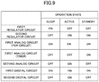
- FIG. 9 is a diagram illustrating an example of the state of each circuit in operation states.
- the regulator circuit is required to have a current capability corresponding to a load of a lord circuit to which an internal voltage is supplied.
- the load of the load circuit to which the internal voltage is supplied, by the regulator circuit varies according to an operation state of the apparatus.
- the load during an active time becomes heavier loading than that during a sleep time.
- the regulator circuit is required to be designed to have the current capability to withstand the load during the active time.
- the present disclosure has an object to avoid wasteful power consumption for an integrated circuit apparatus provided with regulator circuits.
- wasteful power consumption for an integrated circuit apparatus provided with regulator circuits can be avoided.
- FIG. 1 is a block diagram illustrating an example of the configuration of an integrated circuit apparatus according to one embodiment.
- the integrated circuit apparatus 100 is an analog front end (AFE) that drives a sensor 200 and that controls an analog sensor signal from the sensor 200 .
- the integrated circuit apparatus 100 is coupled between a digital signal processor (not illustrated) such as a microcomputer, and the sensor 200 .
- the integrated circuit apparatus 100 is a semiconductor integrated circuit formed with a semiconductor chip.
- the integrated circuit apparatus 100 includes a first regulator circuit 110 ; a second regulator circuit 120 ; a first analog circuit 130 ; a second analog circuit 140 ; a first digital circuit 150 ; and a second digital circuit 160 .
- Each of the first regulator circuit 110 and the second regulator circuit 120 decreases a power supply voltage VDD that is supplied to the integrated circuit apparatus 100 , via a terminal P 1 , from the outside (a microcomputer or the like), to thereby produce a regulated voltage VRG. Further, each of the first regulator circuit 110 and the second regulator circuit 120 supplies, as an internal voltage, the regulated voltage VRG to each component within the integrated circuit apparatus 100 .
- Each of the first regulator circuit 110 and the second regulator circuit 120 is a linear regulator, as described below in detail.
- the power consumption for the first regulator circuit 110 is less than the power consumption for the second regulator circuit 120 .
- the first regulator circuit 110 or the second regulator circuit 120 is selected such that one regulator circuit from among the first regulator circuit and the second regulator circuit is in an on-state and the other regulator circuit is in an off-state.
- the second regulator circuit 120 When a current passing through a load is greater than or equal to a predetermined load current, the second regulator circuit 120 is turned on.
- the current passing through the load is less than a predetermined load current, the first regulator circuit 110 is turned on.
- the regulators may be switched according to the magnitude of a load current that is detected by a current detecting circuit.
- a control circuit may switch the regulators according to a given operation state of the load, without monitoring the load.
- the regulated voltage VRG generated by the first regulator circuit 110 or the second regulator circuit 120 is applied to a terminal P 2 .
- An external loading capacitance 170 is applied to the terminal P 2 .
- the first analog circuit 130 includes a power-on reset (POR) circuit as a voltage monitoring circuit; a timer; and the like.
- the voltage monitoring circuit performs control to maintain the entire integrated circuit apparatus 100 in a reset state, until a power supply voltage level is stabilized.
- the voltage monitoring circuit operates during both of an active time and a sleep time, as described below.
- the timer operates during the active time, while an analog-to-digital (A/D) conversion circuit 143 (see FIG. 2 ) included in the second regulator circuit 120 intermittently operates. The timer stops during the sleep time.
- A/D analog-to-digital
- the second analog circuit 140 performs a process of converting an analog sensor signal input from the sensor 200 , via a terminal. P 3 .
- FIG. 2 is a diagram illustrating an example of the detailed configuration of the second analog circuit 140 , the first digital circuit 150 , the second digital circuit 160 , and the sensor 200 .
- the sensor 200 is a type of MEMS sensor, for example.
- the sensor 200 is a humidity sensor that measures relative humidity.
- the sensor 200 includes a humidity-detection capacitor 201 of which capacitance varies according to humidity, and includes a reference capacitor 202 of which capacitance is constant regardless of humidity.
- the humidity-detection capacitor 201 is coupled between a terminal P 3 a and a terminal P 4 .
- the reference capacitor 202 is coupled between a terminal P 3 b and the terminal P 4 .
- the terminal P 3 a and the terminal P 3 b correspond to the terminal P 3 illustrated in FIG. 1 .
- the second analog circuit 140 includes a drive circuit 141 ; a capacitance-to-voltage (CV) conversion circuit 142 ; the A/D conversion circuit 143 ; and the like.
- the drive circuit 141 generates a first drive signal DRV 1 that is an AC drive signal having a rectangular waveform, as well as a second drive signal DRV 2 that is an AC drive signal having a rectangular waveform.
- the second drive signal DRV 2 has a phase opposite the first drive signal DRV 1 .
- the drive circuit 141 applies the first drive signal DRV 1 to the humidity-detection capacitor 20 via the terminal P 3 a .
- the drive circuit 141 applies the second drive signal DRV 2 to the reference capacitor 202 via the terminal P 3 b.
- a period during which the first drive signal DRV 1 is at high level and the second drive signal DRV 2 is at low level is referred to as a first charge transfer period.
- a period during which the first drive signal DRV 1 is at low level and the second drive signal DRV 2 is at high level is referred to as a second charge transfer period.
- the CV conversion circuit 142 is a charge-voltage conversion circuit in a switched capacitor system.
- the CV conversion circuit 142 acquires a signal charge output from the sensor 200 , during the first charge transfer period, as well as a signal charge output from the sensor 200 , during the second charge transfer period. During each charge transfer period, the signal charge is acquired through the terminal P 4 .
- the CV conversion circuit 142 converts each of the acquired signal charges into a voltage, and outputs the voltage to the A/D conversion circuit 143 .
- the A/D conversion circuit 143 is a differential input AD converter.
- the A/D conversion circuit 143 converts a difference value of the magnitude between the two voltages input from the CV conversion circuit 142 , into a digital signal.
- the A/D conversion circuit 143 outputs the difference value.
- the difference value corresponds to a measured value of relative humidity.
- the digital signal output from the A/D conversion circuit 143 is input to the second digital circuit 160 .
- the second digital circuit 160 includes a correction calculation circuit 161 ; a non-volatile storage unit 162 ; and the like.
- the correction calculation circuit 161 is a digital filter that correctly calculates the digital signal input from the second analog circuit 140 .
- the non-volatile storage unit 162 is a semiconductor memory such as a flash memory. The non-volatile storage unit 162 stores the digital signal (sensor value) that the correction calculation circuit 161 correctly calculates.
- the second digital circuit 160 is coupled to the first regulator circuit 110 and the second regulator circuit 120 (see FIG. 1 ).
- a switch SW illustrated in FIG. 1 is turned on or off in accordance with the enable signal EN 2 described below, the enable signal EN 2 being output from the first digital circuit 150 .
- the switch SW is in an on-state during the active time described below.
- the switch SW is provided to reduce leakage current during the sleep time.
- the first digital circuit 150 includes a control circuit 151 ; a register 152 ; a communication circuit 153 ; and the like.
- the control circuit 151 controls each component within the integrated circuit apparatus 100 .
- the second analog circuit 140 and the second digital circuit 160 are each controlled by the control circuit 151 .
- Each of the second analog circuit 140 and the second digital circuit 160 operates during the active time during which the sensor value is acquired. In contrast, each of the second analog circuit 140 and the second digital circuit 160 does not operate during the sleep time during which the sensor value is not acquired.
- the register 152 stores various information.
- the communication circuit 153 is a communication circuit that performs communication in a serial transmission system such as inter-integrated circuit (I2C) communication.
- the communication circuit 153 performs data communication with the non-volatile storage unit 162 or an external microcomputer. In a manner such that the communication circuit 153 always performs data communication with the external microcomputer, the first digital circuit 150 is configured to operate even during the sleep time.
- I2C inter-integrated circuit
- FIG. 3 is a block diagram illustrating an example of the configuration of the first regulator circuit 110 and the second regulator circuit 120 .
- the regulated voltage generated by the first regulator circuit 110 is referred to as a first regulated voltage VRG 1
- the regulated voltage generated by the second regulator circuit 120 is referred to as a second regulated voltage VRG 2 .
- the first regulated voltage VRG 1 and the second regulated voltage VRG 2 are set at the same voltage level.
- the first regulator circuit 110 includes a first circuit unit 111 and a first output stage 112 .
- the first regulator circuit 110 is a linear regulator.
- a voltage level of the first regulated voltage VRG 1 that is generated by the first regulator circuit 110 is monitored by the voltage monitoring circuit included in the first analog circuit 130 that is coupled to the first circuit unit 111 .
- the first circuit unit 111 is always in an on-state while the integrated circuit apparatus 100 is operating.
- the first output stage 112 is turned on or off in accordance with the enable signal EN 1 input from the second regulator circuit 120 .
- the second regulator circuit 120 includes a second circuit unit. 121 , a second output stage 122 , and a NAND circuit 123 .
- the second regulator circuit 120 is a linear regulator.
- the second circuit unit 121 and the second output stage 122 are each turned on or off in accordance with the enable signal EN 2 input from the control circuit 151 included in the first digital circuit 150 .
- the voltage monitoring circuit included in the first analog circuit 130 that is coupled to the second circuit unit 121 monitors the voltage level of the second regulated voltage VRG 2 generated by the second regulator circuit 120 .
- a power good-signal generating unit outputs a power good signal PG in accordance with the voltage level monitored by the voltage monitoring circuit; and with a level of the current applied by a given regulator. Specifically, after the second circuit unit 121 and the second output stage 122 have become in an on-state, the voltage monitoring circuit causes the power good signal PG to be at low level until the second regulated voltage VRG 2 reaches a reference value. In contrast, when the second regulated voltage VRG 2 reaches the reference value, the voltage monitoring circuit causes the power good signal PG to be at high level.
- the enable signal EN 2 and the power good signal PG are input to the NAND circuit 123 .
- the NAND circuit 123 outputs the enable signal EN 1 at a level that is obtained by a non-conjunction of the enable signal EN 2 and the power good signal PG.
- the NAND circuit 123 when the enable signal EN 2 is at low level, the NAND circuit 123 outputs the enable signal EN 1 at high level, regardless of the level of the power good signal PG. When the enable signal EN 2 is at high level, the NAND circuit 123 outputs the enable signal EN 1 at high level until the power good signal PG is changed to a high level. When the power good signal PG becomes at high level, the NAND circuit 123 outputs the enable signal EN 1 at low level.
- the first output stage 112 of the first regulator circuit 110 becomes in an off-state, in response to inputting the enable signal EN 1 at Low level.
- FIG. 4 is a circuit diagram illustrating an example of the linear regulator that constitutes each of the first regulator circuit 110 and the second regulator circuit 120 .
- the linear regulator includes an output transistor TR; feedback resistors R 1 and R 2 ; and an operational amplifier OP as a difference amplifier.
- the output transistor TR is, for example, a P-channel MOS transistor.
- a source and a drain are coupled between the terminal P 1 as an input source to which the power supply voltage VDD is applied, and the terminal P 2 from which the regulated voltage VRG is output.
- a gate of the output transistor TR is coupled to an output terminal of the operational amplifier OP.
- the feedback resistors R 1 and R 2 are coupled in series between the terminal P 2 and a ground.
- a feedback voltage Vfb obtained by dividing the regulated voltage VRG is applied to a positive terminal of the operational amplifier OP.
- a reference voltage Vref is applied to a negative terminal of the operational amplifier OP, by a reference voltage source.
- the operational amplifier OP outputs a voltage Vo obtained by amplifying a differential voltage associated with the two input terminals (positive terminal and the negative terminal).
- the output voltage Vo is applied to the gate of the output transistor TR.
- the operational amplifier OP decreases the output voltage Vo when the feedback voltage Vfb is higher than the reference voltage Vref.
- the operational amplifier OP increases the output voltage Vo when the feedback voltage Vfb is lower than or equal to the reference voltage Vref.
- An on resistance associated with the output transistor TR is controlled according to the output voltage Vo, so that the regulated voltage is maintained at a level at which the voltage is constant (target voltage).
- the output transistor TR is included in each of the first output stage 112 and the second output stage 122 described above.
- the operational amplifier OP is included in each of the first circuit unit 111 and the second circuit unit 121 .
- the first regulator circuit 110 and the second regulator circuit 120 differ in a current capability of each of the output transistor TR and the operational amplifier OP.
- the output transistor TR of the second regulator circuit 120 has an increased drive capability than the output transistor TR of the first regulator circuit 110 .
- the current passing through the operational amplifier OP of the second regulator circuit 120 is larger than the current passing through the operational amplifier OP of the first regulator circuit 110 .
- FIG. 5 is a diagram illustrating an example of the operation of the first regulator circuit 110 for which power consumption is low.
- FIG. 5 (A) illustrates a time change in the output voltage Vo of the operational amplifier OP.
- FIG. 5 (B) illustrates a time change in the first regulated voltage VRG 1 that is generated by the first regulator circuit 110 .
- the current of the operational amplifier OP is small, and the output transistor TR has a small drive capability.
- the first regulated voltage VRG 1 varies according to variation in the power supply voltage VDD or the load, a time required for a feedback is long.
- the output voltage Vo applied to the gate of the output transistor TR varies greatly between a high level (H) and a low level (L), as illustrated in FIG. 5 (A).
- the first regulator circuit 110 serves substantially as a comparator, so that the first regulated voltage VRG 1 varies greatly relative to the target voltage, as illustrated in FIG. 5(B) .
- the first regulator circuit 110 advantageously allows for decreased power consumption.
- accuracy of the first regulated voltage VRG 1 relative to the target voltage decreases.
- the first regulator circuit 110 because a responsiveness is not high, when heavy loading is applied to the terminal. P 2 , the first regulated voltage VRG 1 may decrease below a reset voltage before the output transistor TR is turned on.
- FIG. 6 is a diagram illustrating an example of the operation of the second regulator circuit 120 for which power consumption is high.
- FIG. 6(A) illustrates a time change in the output voltage Vo of the operational amplifier OP.
- FIG. 6 (B) illustrates a time change in the second regulated voltage VRG 2 that is generated by the second regulator circuit 120 .
- the current of the operational amplifier OP is large and the output transistor TR has a large drive capability.
- the second regulated voltage VRG 2 varies according to variation in the power supply voltage VDD or the load, a time required for a feedback decreases.
- the output voltage Vo applied to the gate of the output transistor TR is almost unchanged relative to a constant voltage, as illustrated in FIG. 6 (A).
- a magnitude change relative to the target voltage decreases, as illustrated in FIG. 6(B) .
- a rate of voltage variation at a time of heavy loading decreases in comparison to the first regulated voltage VRG 1 .
- the power consumption for the second regulator circuit 120 is high.
- the second regulator circuit 120 advantageously allows for increased accuracy of the second regulated voltage VRG 2 relative to the target voltage, as well as decreased noise.
- FIG. 7 is a timing diagram for explaining an example of the operation timing of the first regulator circuit 110 and the second regulator circuit 120 .
- FIG. 7(A) is a diagram illustrating the time change in the power supply voltage VDD.
- FIG. 7 (B) is a diagram illustrating the time change in the first regulated voltage VRG 1 that is generated by the first regulator circuit 110 .
- FIG. 7 (C) is a diagram illustrating the time change in the second regulated voltage VRG 2 that is generated by the second regulator circuit 120 .
- FIG. 7(D) is a diagram illustrating the time change in the regulated voltage VRG that is generated as the internal voltage, the regulated voltage VRG being based on the result in which the first regulated voltage VRG 1 or the second regulated voltage VRG 2 is selected.
- FIG. 7(E) is a diagram illustrating the time change in the enable signal EN 2 that is input to the first regulator circuit 110 from the control circuit 151 .
- FIG. 7(F) is a diagram illustrating the time change in the power good signal PG that is generated by the power good-signal generating unit of the second regulator circuit 120 .
- FIG. 7 (G) is a diagram illustrating the time change in the enable signal EN 1 that is input to the first regulator circuit 110 from the second regulator circuit 120 .
- FIG. 7(H) is a diagram illustrating the load current (VRG load current) passing through the load that is coupled to the terminal P 2 .
- the first regulator circuit 110 and the second regulator circuit 120 are controlled by the control circuit 151 .
- the control circuit 151 supplies the enable signal EN 2 at low level to the second regulator circuit 120 .
- the control circuit 151 causes the first regulator circuit 110 to transition from an off-state to an on-state, while causing the second regulator circuit 120 to be in an off-state.
- the integrated circuit apparatus 100 is in a start state until the first regulated voltage VRG 1 reaches a predetermined voltage.
- the integrated circuit apparatus 100 is in a sleep state, so that the sensor value is not acquired. In other words, the second analog circuit 140 and the second digital circuit 160 do not operate to acquire the sensor value.
- the second regulator circuit 120 When the enable signal. EN 2 becomes at high level, the second regulator circuit 120 starts.
- the voltage monitoring circuit included in the first analog circuit 130 monitors the voltage level of the second regulated voltage VRG 2 .
- the enable signal EN 1 output from the NAND circuit 123 changes to a low level, because the enable signal EN 2 is at high level.
- the enable signal EN 1 input to the first regulator circuit 110 becomes at low level
- the first output stage 112 of the first regulator circuit 110 becomes in an off-state.
- the second regulated voltage VRG 2 generated by the second regulator circuit 120 is used as the internal voltage.
- the integrated circuit apparatus 100 becomes in an active state so that the second analog circuit 140 and the second digital circuit 160 are each turned on by the control circuit 151 . Accordingly, the sensor value is acquired.
- the second regulator circuit 120 stops. Further, the enable signal EN 1 output from the NAND circuit 123 becomes at high level, so that the first output stage 112 of the first regulator circuit 110 becomes in an on-state. Thereby, the integrated circuit apparatus 100 again becomes in the sleep state. Accordingly, the first regulated voltage VRG 1 generated by the first regulator circuit 110 is used as the internal voltage.
- FIG. 8 is a diagram illustrating an example of the detailed operation during the active time.
- FIG. 8A is a diagram illustrating variation in the VRG load current during the active time.
- the active period (period from t 4 to t 5 ) illustrated in FIG. 7 includes an active period during which the A/D conversion circuit 143 operates; and a standby period during which the A/D conversion circuit 143 stops.
- the standby period is measured by the timer included in the first analog circuit 130 .
- the length of the standby period as well as the number of active periods may be appropriately modified by setting.
- the VRG load current increases in the active period during which the A/D conversion circuit 143 operates, while decreasing in the standby period. In such a manner, the A/D conversion circuit 143 operates intermittently using the timer, so that the power consumption for the integrated circuit apparatus 100 decreases.
- FIG. 9 is a table illustrating an example of the state of each circuit in the operation states.
- the sleep state only the first regulator circuit 110 ; the voltage monitoring circuit (POR circuit) of the first analog circuit 130 ; and the first digital circuit 150 are in an on-state.
- the sleep state an internal voltage of high accuracy and low noise is not required.
- the first regulator circuit 110 for which power consumption is low is in an on-state.
- the first regulated voltage VRG 1 is used as the internal voltage.
- the second regulator circuit 120 In the active state, the second regulator circuit 120 ; the voltage monitoring circuit (POR circuit) of the first analog circuit 130 ; the second analog circuit 140 ; the first digital circuit 150 ; and the second digital circuit 160 are each in an on-state.
- the active state involves the period during which the sensor value is mainly acquired. In such a state, because an internal voltage of high accuracy and low noise is required, the second regulator circuit 120 is in an on-state. Thereby, the second regulated voltage VRG 2 allowing for high accuracy and low noise is used as the internal voltage.
- the second regulator circuit 120 In the standby state, the second regulator circuit 120 ; the voltage monitoring circuit (POR circuit) of the first analog circuit 130 ; the timer of the first analog circuit 130 ; and the first digital circuit 150 are each in an on-state. In the standby state as well, the second regulated voltage VRG 2 is used as the internal voltage.
- the second regulator circuit 120 that generates the second regulated voltage VRG 2 allowing for high accuracy and decreased noise is selected during the active time (during the active time and the standby time).
- the first regulator circuit 110 for which power consumption is low is selected. Thereby, wasteful power consumption is minimized.
- either of the first regulator circuit 110 or the second regulator circuit 120 is exclusively selected. Further, as illustrated in FIG. 7 , in the period (period from t 3 to t 4 ) during which the integrated circuit apparatus 100 is transitioned from the sleep state to the active state, the enable signals EN 1 and EN 2 are both set to be at high level, so that both of the first regulator circuit 110 and the second regulator circuit 120 operate.
- the first regulator circuit 110 and the second regulator circuit 120 both operate such that the regulated voltage VRG 1 does not decrease to the reset voltage.
- the second regulator circuit 120 is turned off and synchronously the first regulator circuit 110 is turned on.
- the load current instantaneously decreases so that the internal voltage does not thereby drop below the reset voltage.
- the first regulator circuit 110 because only the first output stage 112 is turned off in the active period (period from t 4 to t 5 ), a time required for a return to a normal state decreases when the first regulator circuit 110 is turned on. This is one reason that the second regulator circuit 120 is turned off and synchronously the first regulator circuit 110 is turned on.
- control circuit 151 supplies the enable signal EN 2 to the second regulator circuit 120 , and the second regulator circuit 120 supplies the enable signal EN 1 to the first regulator circuit 110 .
- control circuit 151 may respectively supply the enable signal EN 1 and the enable signal EN 2 to the first regulator circuit 110 and the second regulator circuit 120 , at the timing illustrated in FIG. 7 .
- the senor 200 is a humidity sensor.
- the sensor 200 is not limited to the humidity sensor, and may include a pressure sensor, a temperature sensor, an air flow sensor, or the like.
Landscapes
- Engineering & Computer Science (AREA)
- Power Engineering (AREA)
- Physics & Mathematics (AREA)
- Electromagnetism (AREA)
- General Physics & Mathematics (AREA)
- Radar, Positioning & Navigation (AREA)
- Automation & Control Theory (AREA)
- Continuous-Control Power Sources That Use Transistors (AREA)
Abstract
Description
Claims (18)
Applications Claiming Priority (3)
| Application Number | Priority Date | Filing Date | Title |
|---|---|---|---|
| JP2019137128A JP7435968B2 (en) | 2019-07-25 | 2019-07-25 | integrated circuit device |
| JP2019-137128 | 2019-07-25 | ||
| JPJP2019-137128 | 2019-07-25 |
Publications (2)
| Publication Number | Publication Date |
|---|---|
| US20210028699A1 US20210028699A1 (en) | 2021-01-28 |
| US11290013B2 true US11290013B2 (en) | 2022-03-29 |
Family
ID=74189186
Family Applications (1)
| Application Number | Title | Priority Date | Filing Date |
|---|---|---|---|
| US16/931,829 Active 2040-08-14 US11290013B2 (en) | 2019-07-25 | 2020-07-17 | Integrated circuit apparatus including regulator circuits |
Country Status (3)
| Country | Link |
|---|---|
| US (1) | US11290013B2 (en) |
| JP (1) | JP7435968B2 (en) |
| CN (1) | CN112311230A (en) |
Families Citing this family (2)
| Publication number | Priority date | Publication date | Assignee | Title |
|---|---|---|---|---|
| EP3993249A1 (en) * | 2020-10-28 | 2022-05-04 | NXP USA, Inc. | Advanced power supply to insure safe behavior of an inverter application |
| US20250076912A1 (en) * | 2023-08-30 | 2025-03-06 | Apple Inc. | Regulator system with voltage control |
Citations (9)
| Publication number | Priority date | Publication date | Assignee | Title |
|---|---|---|---|---|
| JP2001211640A (en) | 2000-01-20 | 2001-08-03 | Hitachi Ltd | Electronic device, semiconductor integrated circuit, and information processing system |
| US6560157B2 (en) | 2000-12-08 | 2003-05-06 | Mitsubishi Denki Kabushiki Kaisha | Semiconductor device |
| US20040174149A1 (en) * | 2002-07-25 | 2004-09-09 | Hideki Agari | Power supplying methods and apparatus that provide stable output voltage |
| US20090295344A1 (en) * | 2008-05-29 | 2009-12-03 | Apple Inc. | Power-regulator circuit having two operating modes |
| US20130169246A1 (en) * | 2011-12-28 | 2013-07-04 | Skymedi Corporation | Linear voltage regulating circuit adaptable to a logic system |
| JP2014106990A (en) | 2012-11-28 | 2014-06-09 | Seiko Epson Corp | Integrated circuit device, oscillation device, and electronic apparatus |
| US20170063229A1 (en) * | 2015-09-01 | 2017-03-02 | Silicon Laboratories Inc. | Providing Multiple Power Paths In An Integrated Circuit |
| US20200158675A1 (en) | 2018-11-16 | 2020-05-21 | Minebea Mitsumi Inc. | Sensor |
| US20200158676A1 (en) | 2018-11-16 | 2020-05-21 | Minebea Mitsumi Inc. | Detecting device, method for controlling detecting device and circuit for converting charge into voltage |
Family Cites Families (4)
| Publication number | Priority date | Publication date | Assignee | Title |
|---|---|---|---|---|
| JPH06168038A (en) * | 1992-12-01 | 1994-06-14 | Fujitsu Ltd | Power supply |
| JP2004133800A (en) * | 2002-10-11 | 2004-04-30 | Renesas Technology Corp | Semiconductor integrated circuit device |
| JP4246045B2 (en) * | 2003-12-02 | 2009-04-02 | 株式会社リコー | Power supply circuit and method for raising output voltage of power supply circuit |
| JP3710468B1 (en) * | 2004-11-04 | 2005-10-26 | ローム株式会社 | Power supply device and portable device |
-
2019
- 2019-07-25 JP JP2019137128A patent/JP7435968B2/en active Active
-
2020
- 2020-07-16 CN CN202010687932.3A patent/CN112311230A/en active Pending
- 2020-07-17 US US16/931,829 patent/US11290013B2/en active Active
Patent Citations (11)
| Publication number | Priority date | Publication date | Assignee | Title |
|---|---|---|---|---|
| JP2001211640A (en) | 2000-01-20 | 2001-08-03 | Hitachi Ltd | Electronic device, semiconductor integrated circuit, and information processing system |
| US6424128B1 (en) | 2000-01-20 | 2002-07-23 | Hitachi, Ltd. | Electronic device having power supply regulators controlled according to operation mode of internal circuit |
| US6560157B2 (en) | 2000-12-08 | 2003-05-06 | Mitsubishi Denki Kabushiki Kaisha | Semiconductor device |
| JP4583588B2 (en) | 2000-12-08 | 2010-11-17 | ルネサスエレクトロニクス株式会社 | Semiconductor device |
| US20040174149A1 (en) * | 2002-07-25 | 2004-09-09 | Hideki Agari | Power supplying methods and apparatus that provide stable output voltage |
| US20090295344A1 (en) * | 2008-05-29 | 2009-12-03 | Apple Inc. | Power-regulator circuit having two operating modes |
| US20130169246A1 (en) * | 2011-12-28 | 2013-07-04 | Skymedi Corporation | Linear voltage regulating circuit adaptable to a logic system |
| JP2014106990A (en) | 2012-11-28 | 2014-06-09 | Seiko Epson Corp | Integrated circuit device, oscillation device, and electronic apparatus |
| US20170063229A1 (en) * | 2015-09-01 | 2017-03-02 | Silicon Laboratories Inc. | Providing Multiple Power Paths In An Integrated Circuit |
| US20200158675A1 (en) | 2018-11-16 | 2020-05-21 | Minebea Mitsumi Inc. | Sensor |
| US20200158676A1 (en) | 2018-11-16 | 2020-05-21 | Minebea Mitsumi Inc. | Detecting device, method for controlling detecting device and circuit for converting charge into voltage |
Also Published As
| Publication number | Publication date |
|---|---|
| US20210028699A1 (en) | 2021-01-28 |
| CN112311230A (en) | 2021-02-02 |
| JP7435968B2 (en) | 2024-02-21 |
| JP2021022067A (en) | 2021-02-18 |
Similar Documents
| Publication | Publication Date | Title |
|---|---|---|
| US6573693B2 (en) | Current limiting device and electrical device incorporating the same | |
| US7688047B2 (en) | Power circuit and method of rising output voltage of power circuit | |
| CN100375134C (en) | Display device with temperature compensating function | |
| US8508196B2 (en) | Switching regulator | |
| US7550955B2 (en) | Power supply circuit | |
| US8264294B2 (en) | Semiconductor device having on-chip oscillator for producing clock signal | |
| US20070241732A1 (en) | Power management system with multiple power sources | |
| EP2713234A1 (en) | A low power low dropout linear voltage regulator | |
| US6300820B1 (en) | Voltage regulated charge pump | |
| US9800157B2 (en) | Switching regulator | |
| US11323110B2 (en) | Duty timing detector detecting duty timing of toggle signal, device including duty timing detector, and operating method of device receiving toggle signal | |
| US9425685B2 (en) | DC-DC voltage converter and conversion method | |
| US9601987B2 (en) | Power supply apparatus | |
| US11290013B2 (en) | Integrated circuit apparatus including regulator circuits | |
| US10613122B2 (en) | Monitoring circuit and semiconductor device | |
| US20050243623A1 (en) | Circuit arrangement for voltage regulation | |
| US9933798B2 (en) | Voltage regulator | |
| US11146110B2 (en) | Power reception device | |
| US10110039B2 (en) | Cancel voltage offset of operational amplifier | |
| US8310091B2 (en) | Monitoring system and input and output device thereof | |
| US20260003379A1 (en) | Low dropout regulator, semiconductor device including same and method of controlling same | |
| JP2023064354A (en) | Battery-less sensor circuit | |
| US20140285168A1 (en) | Adjustable voltage output device and adjustment method of operating voltage | |
| JP2021170870A (en) | Electronic control device |
Legal Events
| Date | Code | Title | Description |
|---|---|---|---|
| AS | Assignment |
Owner name: MINEBEA MITSUMI INC., JAPAN Free format text: ASSIGNMENT OF ASSIGNORS INTEREST;ASSIGNOR:YAMAMOTO, KOSUKE;REEL/FRAME:053240/0312 Effective date: 20200709 |
|
| FEPP | Fee payment procedure |
Free format text: ENTITY STATUS SET TO UNDISCOUNTED (ORIGINAL EVENT CODE: BIG.); ENTITY STATUS OF PATENT OWNER: LARGE ENTITY |
|
| STPP | Information on status: patent application and granting procedure in general |
Free format text: DOCKETED NEW CASE - READY FOR EXAMINATION |
|
| STPP | Information on status: patent application and granting procedure in general |
Free format text: NON FINAL ACTION MAILED |
|
| STPP | Information on status: patent application and granting procedure in general |
Free format text: RESPONSE TO NON-FINAL OFFICE ACTION ENTERED AND FORWARDED TO EXAMINER |
|
| STPP | Information on status: patent application and granting procedure in general |
Free format text: PUBLICATIONS -- ISSUE FEE PAYMENT VERIFIED |
|
| STCF | Information on status: patent grant |
Free format text: PATENTED CASE |
|
| MAFP | Maintenance fee payment |
Free format text: PAYMENT OF MAINTENANCE FEE, 4TH YEAR, LARGE ENTITY (ORIGINAL EVENT CODE: M1551); ENTITY STATUS OF PATENT OWNER: LARGE ENTITY Year of fee payment: 4 |