US11287366B2 - Scanning microwave ellipsometer and performing scanning microwave ellipsometry - Google Patents
Scanning microwave ellipsometer and performing scanning microwave ellipsometry Download PDFInfo
- Publication number
- US11287366B2 US11287366B2 US16/864,466 US202016864466A US11287366B2 US 11287366 B2 US11287366 B2 US 11287366B2 US 202016864466 A US202016864466 A US 202016864466A US 11287366 B2 US11287366 B2 US 11287366B2
- Authority
- US
- United States
- Prior art keywords
- microwave
- sample
- microwave radiation
- sensor
- ellipsometer
- Prior art date
- Legal status (The legal status is an assumption and is not a legal conclusion. Google has not performed a legal analysis and makes no representation as to the accuracy of the status listed.)
- Active, expires
Links
Images


Classifications
-
- G—PHYSICS
- G01—MEASURING; TESTING
- G01N—INVESTIGATING OR ANALYSING MATERIALS BY DETERMINING THEIR CHEMICAL OR PHYSICAL PROPERTIES
- G01N21/00—Investigating or analysing materials by the use of optical means, i.e. using sub-millimetre waves, infrared, visible or ultraviolet light
- G01N21/17—Systems in which incident light is modified in accordance with the properties of the material investigated
- G01N21/21—Polarisation-affecting properties
- G01N21/211—Ellipsometry
-
- G—PHYSICS
- G01—MEASURING; TESTING
- G01N—INVESTIGATING OR ANALYSING MATERIALS BY DETERMINING THEIR CHEMICAL OR PHYSICAL PROPERTIES
- G01N22/00—Investigating or analysing materials by the use of microwaves or radio waves, i.e. electromagnetic waves with a wavelength of one millimetre or more
- G01N22/02—Investigating the presence of flaws
Definitions
- a scanning microwave ellipsometer comprising: a microwave ellipsometry test head comprising: a polarization controller that receives an input electrical signal, produces a polarization-controlled microwave radiation from the input electrical signal, receives reflected microwave radiation resulting from the polarization-controlled microwave radiation, and produces output electrical signal from reflected microwave radiation; a transmission line in communication with the polarization controller and that receives the polarization-controlled microwave radiation from the polarization controller, produces transmitted microwave radiation from the polarization-controlled microwave radiation, receives sensor-received microwave radiation resulting from the transmitted microwave radiation, and produces a reflected microwave radiation from the sensor-received microwave radiation; and a sensor in communication with the transmission line and that receives the transmitted microwave radiation from the transmission line, produces sensor microwave radiation from the transmitted microwave radiation, subjects a sample to the sensor microwave radiation, receives a sample-reflected microwave radiation from the sample that results from subjecting the sample with sensor microwave radiation, and produces a sensor-received microwave radiation from the sample-reflected
- a microwave ellipsometer calibrant to calibrate a scanning microwave ellipsometer, the microwave ellipsometer calibrant comprising: a substrate and a plurality of sectors disposed on the substrate, wherein each sector provides a known material and known positional anisotropy of microwave reflection coefficient ⁇ , wherein the plurality of sectors comprises: a first sector that comprises a first material disposed as first stripes and a second material disposed as second stripes such that the first stripes and the second stripes are alternatingly disposed to provide a first anisotropic sheet resistivity; a second sector that comprises a third material disposed as third stripes and a fourth material disposed as fourth stripes such that the third stripes and the fourth stripes are alternatingly disposed to provide a second anisotropic sheet resistivity; a third sector that comprises a fifth material disposed to provide a first isotropic sheet resistivity; and a fourth sector that comprises a sixth material disposed to provide a second isotropic sheet resistivity.
- a process for performing scanning microwave ellipsometry with the scanning microwave ellipsometer comprising: receiving, by the polarization controller, the input electrical signal; producing, by the polarization controller, the polarization-controlled microwave radiation from the input electrical signal; receiving, by the polarization controller, the reflected microwave radiation resulting from the polarization-controlled microwave radiation; producing, by the polarization controller, the output electrical signal from the reflected microwave radiation; receiving, by the transmission line, the polarization-controlled microwave radiation from the polarization controller; producing, by the transmission line, transmitted microwave radiation from the polarization-controlled microwave radiation; receiving, by the transmission line, the sensor-received microwave radiation resulting from the transmitted microwave radiation; producing, by the transmission line, the reflected microwave radiation from the sensor-received microwave radiation; receiving, by the sensor, the transmitted microwave radiation from the transmission line; producing, by the sensor, the sensor microwave radiation from the transmitted microwave radiation; controlling the polarization of the sensor microwave radiation by the polarization controller; subjecting the
- FIG. 1 shows a scanning microwave ellipsometer
- FIG. 2 shows a microwave ellipsometry test head
- FIG. 3 shows a scanning microwave ellipsometer
- FIG. 4 shows a scanning microwave ellipsometer
- FIG. 5 shows a scanning microwave ellipsometer
- FIG. 6 shows a scanning microwave ellipsometer
- FIG. 7 shows a scanning microwave ellipsometer
- FIG. 8 shows a scanning microwave ellipsometer with a sample for a two-dimensional surface of the sample in panel A, for an irregular three-dimensional surface of the sample in panel B, and for a regular three-dimensional surface of the sample in panel C;
- FIG. 9 shows a microwave ellipsometry test head
- FIG. 10 shows a microwave ellipsometry test head
- FIG. 11 shows a microwave ellipsometry test head
- FIG. 12 shows a microwave ellipsometry test head
- FIG. 13 shows a microwave ellipsometry test head
- FIG. 14 shows a scanning microwave ellipsometer
- FIG. 15 shows a scanning microwave ellipsometer
- FIG. 16 shows a scanning microwave ellipsometer
- FIG. 17 shows a scanning microwave ellipsometer
- FIG. 18 shows an exploded view of a scanning microwave ellipsometer
- FIG. 19 shows a scanning microwave ellipsometer
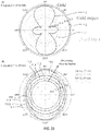
- FIG. 20 shows a microwave ellipsometer calibrant
- FIG. 21 shows magnitude data as a function of angle for isotropic samples, wherein panel A shows data for gold and fused silica samples, and panel B shows data for various MoSi 2 samples;
- FIG. 22 shows magnitude data as a function of angle for anisotropic samples, wherein panel A shows data for gold stripes and fused silica samples, and panel B shows data for various MoSi 2 samples;
- FIG. 23 shows complex data plotted on a smith chart
- FIG. 24 shows a graph of a magnitude of reflection coefficient ⁇ for output electrical signal versus sheet resistance that provides a calibration curve to map reflection coefficient magnitude to sheet resistance
- FIG. 25 shows a graph of an angle of reflection coefficient ⁇ for output electrical signal versus sheet resistance that provides a calibration curve to map reflection coefficient angle to sheet resistance;
- FIG. 26 shows, in panels A and B, measurements of an aligned and misaligned carbon fiber sample before and after mapping to sheet resistance
- FIG. 27 shows physical properties of test wafers
- FIG. 28 shows composite theory with a (a) schematic of the anisotropic composite where the dimensions are defined by voxels (length in nm divided by the voxel edge length a).
- the resistance is dependent on the direction of interest, the subscripts x and y indicate that direction;
- FIG. 29 shows an overview of a full wave simulation with a (a) schematic of the full wave simulation including the material-under-test, the waveguide, the plastic holder, and a box representing the aluminum motor, and (b) match between measurement (solid line with circles) and simulation (dotted line with stars) for the control samples (absorber, fused silica, and gold) over 5 measured heights: (0.3, 0.8, 1.3, 1.8, 2.3) mm;
- FIG. 30 shows an overview of a calibration process with (a) a test-head with the reference planes labeled (first-tier and second-tier) and (b) on a Smith chart with all isotropic materials measured including the controls: gold, fused silica, absorber, and the MoSi 2 on the test wafers.
- the symbols indicate raw S-parameters, S-parameters calibrated to the end of the 2.4 mm coaxial cable before the test-head (first-tier), and the S-parameters calibrated to the edge of the WR-42 waveguide (second-tier), respectively.
- the S-parameters are shown for one angle, where the change over angle is small compared to the size of the plot markers;
- FIG. 31 shows calibrated measurements for control and test samples including the gold, fused silica, different thickness of MoSi 2 , gold stripes on fused silica, and gold stripes on different thickness of MoSi 2 .
- Samples were separated into (a) isotropic gold and absorber and gold stripes on fused silica, and (b) the isotropic MoSi 2 films and gold stripes on MoSi 2 films.
- the polar plot of the magnitude of the reflection coefficient has uncertainties equal to the standard deviation of the measurement between all 16 (x,y)-positions.
- the same data are represented in (c) a Smith chart of the complex impedances for each MUT and (d) a blown-up section of the Smith chart for better visibility;
- FIG. 32 shows sheet resistance tensor components from circuit model analysis, 3d composite simulation, and the mapping function
- FIG. 33 shows a comparison of measured and simulated S-parameters (a) on a Smith chart with measured (solid line) and simulated (dotted line) lines for three of the anisotropic materials, gold stripes on bare fused silica, 20 nm, and 185 nm. (b) The vector magnitude between the measured and simulated S-parameters for each angle between 0° and 360° for all five anisotropic materials;
- FIG. 34 shows a mapping function (a) (gray line) extracted with simulation between complex S-parameters and a 200 nm MUT with an isotropic conductivity with 320 points between 10 9 (S/m) and 10 ⁇ 9 (S/m).
- the stars are the measured response of the isotropic materials gold, MoSi 2 of 185 nm, 80 nm, 45 nm, and 20 nm, and bare fused silica.
- FIG. 35 shows how carbon fibers can be oriented relative to the fundamental model TE 10 of an electric field (arrows) in waveguide.
- the color bar indicates the strength of the electric field in V/m;
- FIG. 36 shows a squared ellipse that models the relative reflected power as a function of angle, where the angle is defined as the angle between the electric field and the sample-under-test.
- the blue solid line is the squared-ellipse fit, ⁇ o is the orientation, a is the minor axis, and b is the major axis;
- FIG. 37 shows a microwave ellipsometry measurement setup.
- FIG. 38 shows selected steps from a process that includes (a) levelling the waveguide flange with a reference flat; (b) aligning an edge of the sample to the edge of graph paper that is affixed to the dielectric spacer with polyimide tape; and (c) rotating the sample;
- FIG. 39 shows four-layer short carbon fiber samples for testing the microwave ellipsometry measurement.
- Sample #1 was identical to the control.
- Sample #2 had all the layers rotated by 5°.
- Sample #3 had the second of four layers rotated by 5°.
- Sample #4 had the second of four layers rotated by 15°;
- FIG. 40 shows microwave ellipsometry data at 18 GHz for no sample, an aluminum sheet, and Sample #2.
- ‘no sample’ case measurements blue circles
- Aluminum case measurements blue circles
- red circle has a radius close to one
- isotropic model red circle
- Sample #3 measurements blue circles
- red circle has an orientation close to 5°, and fits an anisotropic model
- FIG. 41 shows data for blind samples results for orientation ( ⁇ o ) and alignment for ( ⁇ ab ). Uncertainties were rounded up;
- FIG. 42 shows absolute values for the average orientation for control and four blind samples.
- Side A and Side B corresponded to the top-facing and bottom-facing sides, respectively.
- the measurement frequency was 18 GHz;
- FIG. 43 shows absolute values for the average alignment for control and four blind samples.
- Side A and Side B corresponded to the top-facing and bottom-facing sides, respectively.
- the measurement frequency was 18 GHz;
- FIG. 44 shows data for carbon fiber composite samples with extracted parameters
- FIG. 45 shows samples measured for (a) a fabricated ideal sample and (b) a single-layer short carbon fiber, (c) a multiple layer short carbon fiber, (d) a single layer continuous fiber, and (e) multiple layer continuous fiber;
- FIG. 46 shows R( ⁇ ( ⁇ )) for (a) test wafers with gold stripes on different thickness of MoSi 2 and (b) short carbon fiber composites (SCFC) and continuous carbon fiber composites (CCFC);
- FIG. 47 shows (a) a mapping function between ( ⁇ ) and R s ( ⁇ / ⁇ ) with the simulated data, measured data from the test wafers, and the phenomenological fit (black line). (b) The implementation of the mapping function of one spatial position and two different carbon fiber composites. The left-hand plot is ( ⁇ ( ⁇ )) while the right-hand plot is R s ( ⁇ ) on a log scale;
- FIG. 48 shows R s ( ⁇ )( ⁇ / ⁇ ) for (a) single layer short carbon fiber composite (SCFC), (b) multiple layer SCFC, (c) single layer continuous carbon fiber composite (CCFC), and (d) multiple layer CCFC.
- Graphs are for one spatial position and a fit (solid line) over mapped data (dots);
- FIG. 49 shows ( ⁇ ) versus R s including the fit (black line) and measurements for the different carbon fiber composites. Data points are colored based on the composite. The points at the lower end correspond to ⁇ (0°) and ⁇ (90°) for each of the samples;
- FIG. 50 shows a single layer SCFC with (a) the mapped data with fit for one spatial position, (b) the percent error as a function of angle for the same spatial position (c) a plot of the orientation for each spatial position and (d) a plot of the ratio between the sheet resistance across and along the fibers (R sx /R sy );
- FIG. 51 shows multiple layer SCFC with (a) the mapped data with fit for one spatial position, (b) the percent error as a function of angle for the same spatial position, (c) a plot of the orientation for each spatial position, and (d) a plot of the ratio between the sheet resistance across and along the fibers (R sx /R sy );
- FIG. 52 shows a single layer CCFC with (a) the mapped data with fit for one spatial position, (b) the percent error as a function of angle for the same spatial position, (c) a plot of the orientation for each spatial position, and (d) a plot of the ratio between the sheet resistance across and along the fibers (R sx /R sy ); and
- FIG. 53 shows a multiple layer CCFC with (a) the mapped data with fit for one spatial position, (b) the percent error as a function of angle for the same spatial position, (c) a plot of the orientation for each spatial position, and (d) a plot of the ratio between the sheet resistance across and along the fibers (R sx /R sy ).
- a scanning microwave ellipsometer overcomes this problem by providing scanning microwave ellipsometry.
- the scanning microwave ellipsometer provides a polarized electric microwave field and measures reflection of the polarized electric microwave field from a sample as a function of angle. Resulting reflected power plotted versus measured angle on a polar plot has an elliptical shape.
- the scanning microwave ellipsometer includes a test head that rotates the electric microwave field relative to the sample.
- the test head is rastered over the sample, e.g., by a 6-axis robotic arm or other motion manipulator.
- a process for performing microwave ellipsometry acquires data, fits the microwave ellipsometry data, and produces discrete measurands that can be plotted as a function of position in three dimensions, two dimensions, or one dimension.
- the discrete measurands can include a maximum value, a minimum value, an alignment value, and an orientation value. Scanning microwave ellipsometry is broadly applicable where large-scale imaging of material properties is useful as well as single testing cases.
- scanning microwave ellipsometer 200 subjects a sample to scanning microwave ellipsometry.
- scanning microwave ellipsometer 200 includes scanning microwave ellipsometer 200 including: microwave ellipsometry test head 2 including: polarization controller 4 that receives input electrical signal 10 , produces polarization-controlled microwave radiation 30 from input electrical signal 10 , receives reflected microwave radiation 31 resulting from polarization-controlled microwave radiation 30 , and produces output electrical signal 11 from reflected microwave radiation 31 ; transmission line 5 in communication with polarization controller 4 and that receives polarization-controlled microwave radiation 30 from polarization controller 4 , produces transmitted microwave radiation 32 from polarization-controlled microwave radiation 30 , receives sensor-received microwave radiation 33 resulting from transmitted microwave radiation 32 , and produces reflected microwave radiation 31 from sensor-received microwave radiation 33 ; and sensor 6 in communication with transmission line 5 and that receives transmitted microwave radiation 32 from transmission line 5 , produces sensor microwave radiation 34 from transmitted microwave radiation
- position controller 8 adjusts the relative position by moving sensor 6 relative to sample 7 selectively along three orthogonal linear directions and in three independent angular coordinates.
- position controller 8 is in mechanical communication with microwave ellipsometry test head 2 through disposition of microwave ellipsometry test head 2 on position controller 8 .
- position controller 8 is in mechanical communication with sample 7 through disposition of sample 7 on position controller 8 .
- sample 7 is disposed on first position controller 8 . 1
- microwave ellipsometry test head 2 is disposed on second position controller 8 . 2 , wherein first position controller 8 . 1 and second position controller 8 . 2 are independently controlled by electrical signal measurement system 1 respectively via first position control signal 9 . 1 and second position control signal 9 . 2 .
- Sample 7 can be an arbitrary sample such as metal, plastic, glass, ceramic, polymer, alloy, liquid, and the like. Sample 7 can be a single material, or it can be a composite of multiple materials in an arbitrary arrangement.
- a shape of sample 7 can include a planar surface, a regular three-dimensional surface (e.g., a sphere, parallelepiped, icosahedron, truncated shape, and the like), or an irregular three-dimensional surface that is subject to sensor microwave radiation 34 from sensor 6 .
- sensor 6 includes waveguide aperture 13 , waveguide horn antenna 14 , waveguide spot-focusing or gaussian-beam antenna 15 , or a combination of at least one of the foregoing sensors 6 .
- polarization controller 4 includes an orthomode transducer 16 , waveguide rotary joint 17 , or a combination of at least one of the foregoing sensors 6 .
- position controller 8 includes roller 18 on which sample 7 is disposed, wherein roller 18 rotates to move sample 7 relative to sensor 6 of microwave ellipsometry test head 2 .
- position controller 8 includes robotic arm 19 on which sensor 6 is disposed, wherein robotic arm 19 moves sensor 6 relative to sample 7 .
- scanning microwave ellipsometer 200 includes microwave ellipsometer calibrant 20 in communication with sensor 6 from which scanning microwave ellipsometer 200 is calibrated.
- Microwave ellipsometer calibrant 20 includes: substrate 21 and a plurality of sectors disposed on substrate 21 . Each sector provides a known material and known positional anisotropy of microwave reflection coefficient ⁇ .
- the plurality of sectors includes: first sector 22 that includes a first material disposed as first stripes 26 and a second material disposed as second stripes 27 such that first stripes 26 and second stripes 27 are alternatingly disposed to provide a first anisotropic sheet resistivity; second sector 23 that includes a third material disposed as third stripes 28 and a fourth material disposed as fourth stripes 29 such that third stripes 28 and fourth stripes 29 are alternatingly disposed to provide a second anisotropic sheet resistivity; third sector 24 that includes a fifth material disposed to provide a first isotropic sheet resistivity; and fourth sector 25 that includes a sixth material disposed to provide a second isotropic sheet resistivity.
- electrical signal measurement system 1 includes a microwave source and a microwave detector, wherein input electrical signal 10 and output electrical signal 11 are microwave radiation.
- electrical signal measurement system 1 includes a vector network analyzer, and input electrical signal 10 and output electrical signal 11 are microwave radiation.
- electrical signal measurement system 1 includes a scalar network analyzer, and input electrical signal 10 and output electrical signal 11 are microwave radiation.
- the electrical signal measurement system 1 includes a computer that controls a vector network analyzer, scalar network analyzer, microwave source, or microwave detector.
- transmission line 5 supports multiple polarizations.
- Transmission line 5 supports polarized microwave radiation and can be an arbitrary transmission line, e.g., circular waveguide, rectangular waveguide, ridge waveguide, and the like.
- microwave refers to a frequency in from 300 Hz to 3 THz. In an embodiment, microwave radiation is above a cutoff frequency for waveguides in test head 2 and below a frequency at which any waveguide in test head 2 supports more than one propagating mode.
- Scanning microwave ellipsometer 200 can be made in various ways.
- a process for making scanning microwave ellipsometer 200 includes providing sensor 6 ; connecting transmission line 5 to sensor 6 ; connecting polarization controller 4 to transmission line 5 so that sensor 6 is in communication with polarization controller 4 via transmission line 5 ; connecting polarization controller 4 to electrical signal measurement system 1 so that electrical signal measurement system 1 and polarization controller 4 are in communication; connecting electrical signal measurement system 1 to position controller 8 so that electrical signal measurement system 1 and position controller 8 are in communication; optionally disposing sensor 6 proximate to sample 7 so that sensor 6 can subject sample 7 to sensor microwave radiation 34 and so that sensor 6 can receive sample reflected microwave radiation 35 form sample 7 ; and optionally disposing sensor 6 or sample 7 on a position manipulator so that sensor 6 and sample 7 move relative to one another for scanning sensor microwave radiation 34 from sensor 6 over sample 7 .
- a process for performing microwave ellipsometry includes characterizing the S-parameters of the test head as a function of polarization.
- the S-parameters of the test head as a function of polarization are characterized by performing a first-tier one-port coaxial calibration (e.g., a Short-Open-Load calibration) at the end of a coaxial cable that carries an input electrical signal 10 to the test head and carries an output electrical signal 11 from the test head, followed by a second-tier rectangular-waveguide calibration (e.g., a Short-Open-Load calibration) at the end of waveguide aperture 13 for each polarization.
- a first-tier one-port coaxial calibration e.g., a Short-Open-Load calibration
- second-tier rectangular-waveguide calibration e.g., a Short-Open-Load calibration
- the S-parameters of test head 2 are directly obtained from the second-tier calibration error box. This step is performed once for a given test head 2 and is not required every time waveguide ellipsometry is performed if the S-parameters of the test head do not drift appreciably and are retained for future use.
- the process for performing microwave ellipsometry includes performing a first-tier one-port coaxial calibration (e.g., a Short-Open-Load calibration) at the end of a coaxial cable that carries an input electrical signal 10 to the test head and carries an output electrical signal 11 from the test head, followed by cascading the S-parameters of the test head obtained in the first step with the first-tier calibration error box.
- This step can be repeated to correct for drift in the systematic errors introduced by electrical signal measurement system 1 .
- This step includes installation of an electronic calibration unit at the end of a coaxial cable that carries an input electrical signal 10 to the test head and carries an output electrical signal 11 from the test head.
- the process for performing microwave ellipsometry includes placing the sample between the waveguide flange and the dielectric spacer (e.g., Rohacell) ( FIG. 19 ) and aligning microwave ellipsometry test head 2 normal to sample 7 .
- the dielectric spacer can be optional but can simplify implementation of the absorber in simulations, making it advantageous to include for simulations to be performed.
- the process for performing microwave ellipsometry includes measuring a raw complex reflection coefficient at a polarization and with a distance between sensor 6 and sample 7 , at a location on sample 7 .
- a raw complex reflection coefficient is error corrected with the first-tier error box of the prior step cascaded with the S-parameters of the test head from step 1 to obtain an error-corrected magnitude of reflection coefficient ⁇ and an angle of reflection coefficient ⁇ for the material under test.
- the process for performing microwave ellipsometry includes an optional step of repeating the immediate prior two steps for a plurality of sectors of calibrant 20 .
- the process for performing microwave ellipsometry includes an optional step of optimizing a finite element simulation to match the measurements of calibrant 20 .
- Optimized parameters can include a distance between the sample 7 and the waveguide aperture 13 , a thickness and complex permittivity of the dielectric spacer, and a boundary condition corresponding to the absorber under the dielectric spacer.
- the process for performing microwave ellipsometry optionally includes implementing the sample in a finite-element simulation and the material properties of the simulated material-under-test are varied until the simulated error-corrected magnitude of reflection coefficient ⁇ and an angle of reflection coefficient ⁇ for the material under test match the corresponding measured quantities.
- Scanning microwave ellipsometer 200 has numerous advantageous and unexpected benefits and uses.
- a process for performing scanning microwave ellipsometry with scanning microwave ellipsometer 200 includes: receiving, by polarization controller 4 , input electrical signal 10 ; producing, by polarization controller 4 , polarization-controlled microwave radiation 30 from input electrical signal 10 ; receiving, by polarization controller 4 , reflected microwave radiation 31 resulting from polarization-controlled microwave radiation 30 ; producing, by polarization controller 4 , output electrical signal 11 from reflected microwave radiation 31 ; receiving, by transmission line 5 , polarization-controlled microwave radiation 30 from polarization controller 4 ; producing, by transmission line 5 , transmitted microwave radiation 32 from polarization-controlled microwave radiation 30 ; receiving, by transmission line 5 , sensor-received microwave radiation 33 resulting from transmitted microwave radiation 32 ; producing, by transmission line 5 , reflected microwave radiation 31 from sensor-received microwave radiation 33 ; receiving, by sensor 6 , transmitted microwave
- the process further can include determining, from electrical readout signal 12 , the polarization of reflected microwave radiation 31 , magnitude of reflection coefficient ⁇ , and angle of reflection coefficient ⁇ of sample reflected microwave radiation 35 from sample 7 .
- the process can include adjusting, by position controller 8 , relative position by moving sensor 6 relative to sample 7 selectively along three orthogonal linear directions and in three independent angular coordinates.
- the process includes calibrating scanning microwave ellipsometer 200 with microwave ellipsometer calibrant 20 by scanning sensor 6 over sectors over microwave ellipsometer calibrant 20 as microwave ellipsometer calibrant 20 is subjected to sensor microwave radiation 34 ; acquiring sample reflected microwave radiation 35 from microwave ellipsometer calibrant 20 ; and determining angle of reflection coefficient ⁇ and magnitude of reflection coefficient ⁇ for input electrical signal 10 acquired from output electrical signal 11 for sample reflected microwave radiation 35 from microwave ellipsometer calibrant 20 to produce correction factors to apply to an arbitrary output electrical signal 11 acquired from a sample 7 .
- Scanning microwave ellipsometer 200 and processes disclosed herein have numerous beneficial uses, including real-time process control and quality control for composite manufacturing, non-destructive imaging, sub-surface defect detection, and quantitative characterization of anisotropic electrical sheet resistance. These capabilities provide characterizing alignment and orientation of short conductive fibers in composite materials.
- Composites containing short conductive fibers e.g., carbon fibers and carbon nanotubes
- they offer improved mechanical and electrical performance and reduced weight Unfortunately, the structural and electrical integrity of composite parts containing short conductive fibers can be limited by variation in the quality of the feedstock with which they are built. To avoid catastrophic failure, engineers can assume a worst-case performance for a batch of composite material.
- Material-screening provided by scanning microwave ellipsometer 200 is beneficial to tighten tolerance on composite feedstock and formed parts and provide lower cost, lower rate of catastrophic failure, or tighter tolerance for high-performance parts.
- a conventional characterization technique for composites is eddy-current inspection that may not operate at high frequencies where the size of the eddy-current-excitation coil becomes comparable to the wavelength of the probing radiation.
- Increasing measurement frequency above the eddy-current excitation limit can be favorable when the thickness of a material under test is much less than the skin depth at the upper-frequency-limit of the eddy current technique.
- Scanning microwave ellipsometer 200 overcomes this frequency limitation, offering access to an advantageous frequency range.
- the sensitivity of an eddy-current technique decreases rapidly as the distance between an eddy-current-probe coil and a material-under-test increases.
- the distance between sensor 6 and sample 7 can be large compared to the distances available in an eddy-current technique, overcoming the sample-distance limitation.
- Another conventional practice characterizing short-carbon-fiber composites is to image the material on a light table, but light table imaging does not provide quantitative sheet resistance data for analysis and light table imaging can fail when the host matrix is not optically transparent or if the material is too dense, which scanning microwave ellipsometer 200 overcomes.
- Scanning microwave ellipsometer 200 and processes herein unexpectedly facilitate evaluation of composite materials and formed composite parts.
- This evaluation includes qualitative information about the alignment and orientation of conducting fibers in an insulating host matrix and quantitative evaluation of anisotropic electromagnetic materials properties.
- the capability to perform a unique combination of spatially-resolved, anisotropic electrical conductivity measurements, at microwave frequencies, with the option to incorporate a substantial standoff distance between the test head and a material under test, while also allowing for complex formed parts represents a novel departure from conventional processes.
- the measurement speed of scanning microwave ellipsometer 200 is compatible with real-time composite manufacturing techniques, enabling real-time process optimization.
- anisotropic composite materials range from construction composites to electric circuit boards.
- Anisotropic conductivity is one of the many important measurands for anisotropic composites for identifying misalignment.
- waveguide ellipsometry a new electromagnetic characterization technique, and its application to conductive anisotropic composites.
- Typical anisotropic composites include two or more phases where the final material may have a blend of the properties (chemical, mechanical, or electrical) of the original constituents or even a property that is not present in either of the constituent materials (e.g., metamaterials).
- thin conducting anisotropic composites which include sheets of aligned carbon fibers, sheets of aligned carbon nanotubes, and metasurfaces.
- the electrical conductivity can carry critical information about the anisotropic mechanical and thermal properties, making electrical characterization a useful engineering and quality control tool. More broadly, electromagnetic characterization is applicable when at least one material property (e.g., permittivity, permeability, or conductivity) is directional.
- microwave polarimetry is a radar technique where a transmitter or receiver rotates and results in an image of the environment (e.g., precipitation) between the two antennas.
- free-space techniques are extensive in literature, including work on two-port measurements, oblique incidence reflection measurements, one-port frequency shift measurements, and non-destructive inspection.
- non-destructive rectangular waveguide probing on uniaxial anisotropic dielectric materials, and biaxial anisotropic materials where both the permittivity and permeability are tensors.
- the scanning microwave ellipsometer herein characterizes conductively anisotropic materials, including composites, which we called waveguide ellipsometry and probes the conductive anisotropy of the MUT by measuring the reflection coefficient of a linearly polarized electric field ( ⁇ right arrow over (E) ⁇ -field) incident on the MUT.
- the magnitude and phase of the reflected electromagnetic wave depend on the relative orientation of the anisotropic MUT and the polarization of the incident wave. Sweeping the incident polarization direction allows us to probe the material's bulk conductivity tensor (and potentially the permittivity or permeability for broader impact).
- the test-head includes a rotation joint to control the incident polarization direction. Finite-element simulation and composite theory analysis are employed to compute the waveguide fields in lieu of analytic expressions. The measurements and analysis are automated as a function of angle.
- Waveguide ellipsometry is a non-contact, electromagnetic characterization technique ( FIG. 19 ) to characterize material properties.
- test wafer substrates were 150 mm diameter fused silica wafers.
- the metal layers on top of the fused silica were gold (Au) and molybdenum disilicide (MoSi 2 ).
- Au gold
- MoSi 2 molybdenum disilicide
- Quadrant #1 had (10.0 ⁇ 0.5) ⁇ m wide continuous gold stripes on MoSi 2 on a fused silica substrate
- quadrant #2 had (10.0 ⁇ 0.5) ⁇ m continuous gold stripes deposited on the fused silica substrate
- quadrant #3 was a continuous layer of MoSi 2 with no gold stripes
- quadrant #4 was a continuous layer of gold.
- the gold stripes had a center-to-center distance of (20.0 ⁇ 0.5) ⁇ m and were aligned to the defined ⁇ -direction.
- each of the four test wafers had the same four quadrant pattern, however, the thickness of the MoSi 2 , both under the stripes (quadrant #1) and by itself (quadrant #3) ranged from 185 nm to 20 nm to achieve linearly spaced values of the magnitude of the reflection coefficient (
- the first layer MoSi 2
- a sputtering tool We deposited the first layer (MoSi 2 ) with a sputtering tool to have better control over deposition thickness compared to other available tools.
- a standard lift-off process including a wafer wash and a 60 s plasma clean before the deposition of the second layer.
- we spun on a thin layer of adhesion promoter Before adding the photoresist, exposing the pattern, and developing the resist for second layer, we spun on a thin layer of adhesion promoter.
- the plasma clean and adhesion promoter were critical for adhesion of photoresist to MoSi 2 .
- the second layer consisted of a thin layer (20 ⁇ 5) nm of titanium (Ti) for adhesion and a thicker layer (approximately 200 ⁇ 10) nm of gold ( FIG. 27 ).
- FIG. 27 lists measured values for the MoSi 2 thickness, the MoSi 2 sheet resistance, and the second layer (Au and Ti) thickness with the standard deviation for six measurements taken at different locations over the wafers.
- the test wafers were designed to mimic the electrical behavior of real composites.
- the gold stripes are akin to the conducting fibers and the MoSi 2 is akin to a combination of conducting fibers that are misaligned, an electrical percolation network between aligned or misaligned fibers, and the conductivity of the matrix material.
- the smallest dimension of the waveguide is approximately 4.3 mm. This dimension is much larger than the fiber diameter in many conductive-fiber composites and also much larger than the width of the gold stripes in our test wafers. Since the fibers are small compared to the sampled volume, it is reasonable to average out these small features and treat the whole composite as an effective medium with an effective anisotropic conductivity tensor.
- the bulk conductivity tensor can always be represented as a diagonal matrix
- ⁇ ( ⁇ x 0 0 0 ⁇ y 0 0 ⁇ z ) ( 1 )
- ⁇ x , ⁇ y , and ⁇ z are the ⁇ circumflex over (x) ⁇ , ⁇ , and ⁇ circumflex over (z) ⁇ components of the conductivity tensor respectively.
- the conductivity tensor must be rotated by applying a rotation matrix. After applying a rotation matrix around the z-axis by some angle ⁇ , the new conductivity tensor ⁇ rot is,
- ⁇ rot ( A F 0 F B 0 0 0 ⁇ z ) ( 2 )
- A, B, and F are functions of the conductivity tensor components ⁇ x and ⁇ y and ⁇ is the relative angle between the incident ⁇ right arrow over (E) ⁇ -field polarization and the fiber direction.
- This angle rotated conductivity tensor allows us to validate waveguide ellipsometry with full-wave modeling by simplifying the finite-element simulations in the next section. We can also use this form to extract the components ⁇ x and ⁇ y with DC simulation and equivalent circuit modeling.
- Each voxel was assigned an effective conductivity based on the ratio between gold and MoSi 2 .
- the first four anisotropic materials we modeled and measured had some thickness, t, of MoSi 2 .
- the conductivity of the deposited gold was measured with an on-wafer multiline TRL technique and the conductivity of the MoSi 2 was measured with a four-point probe on the blanket films of each test wafer (quadrant #3 in FIG. 20 ).
- we took the conductivity ratio between gold and MoSi 2 to be 280:1 ( ⁇ tilde over ( ⁇ ) ⁇ gn : ⁇ tilde over ( ⁇ ) ⁇ Mn , respectively).
- the DC composite theory simulation computed the bulk conductivity tensor from the model of the composite ( FIG. 28 ) and the conductivity ratio.
- the simulation calculated the voltage at each node and solved the current continuity equations to satisfy the boundary conditions and minimize the dissipated energy over the full system.
- the resistances of each material in the circuit model are related to their length (l), area (A) defined by voxels ( FIG. 28 ), and normalized material conductivity ( ⁇ tilde over ( ⁇ ) ⁇ material ):
- ⁇ ⁇ c ( ⁇ ⁇ materl ⁇ l ⁇ ( A l ) material ) ⁇ 1 / R ⁇ ( l A ) total ( 5 )
- ⁇ (x, y, or z) ⁇ tilde over ( ⁇ ) ⁇ MoSi 2
- R is the total resistance of the circuit model.
- R p n x n y ⁇ ( 200 ⁇ ⁇ ⁇ ⁇ gn ⁇ + t ⁇ ⁇ ⁇ ⁇ gn a ) ( 8 ) and the MoSi 2 resistance (R MoSi 2 ) is:
- the full-wave FEM simulations modeled the measurement setup and calculated the S-parameters from the DC conductivity tensor ( FIG. 29 ).
- the full-wave simulation used an FEM solver to calculate the electromagnetic fields over a specified mesh.
- we imported a 3D model of the rectangular waveguide and the plastic holder on the test-head We did not import the 3D model of the aluminum motor (pictured in FIG. 30 ) because its features were complex to mesh. Instead, we defined a box of aluminum approximately equal in size to the motor in ( ⁇ circumflex over (x) ⁇ , ⁇ ) ( FIG. 29 ) to capture its effect on the electromagnetic fields.
- de-embedding means correcting for the phase and attenuation of the simulated signal. The result is to change the reference plane of the simulation to match the same plane in the measurement.
- the simulated waveguide was at a height, h, above the MUT, which had a thickness, t MUT , and assigned material properties (e.g., conductivity, permittivity).
- material properties e.g., conductivity, permittivity.
- the isotropic gold behaved as a short circuit reflect, however it was not a perfect reflect (
- 1) because there was a gap between the waveguide flange and the materials. This gap allows some of the reflected wave to scatter away from the waveguide flange, but a gap is necessary to make non-contact measurements of the MUT.
- the calibration for waveguide ellipsometry moved the reference plane from somewhere inside the VNA to the end of the WR-42 waveguide for each angle position.
- the calibration procedure was a two-tier calibration ( FIG. 30 ).
- the first-tier was a standard short-open-load (SOL) coaxial calibration to move the reference plane to the coaxial connector before the test-head.
- the second-tier was a WR-42 SOL calibration that rolled the reference plane to the end of the test-head as a function of angle, to account for any affects from the rotary joint on the robot arm that rotated the waveguide.
- the robot was in the same (x,y,z)-position for each calibration and the first MUT measurement position.
- the S-parameters of the test-head are related to the model of the WR-42 calibration devices and the measured S-parameters by:
- ⁇ meas S 11 + ⁇ T ⁇ S 12 ⁇ S 21 1 - S 22 ⁇ ⁇ T ( 10 )
- ⁇ T is the reflection coefficient of a given termination, which includes a short, matched load, and an open.
- ⁇ meas is the measured reflection coefficient for the loads corrected to the 2.4 mm reference plane.
- the three terminations can be expressed by a set of linear equations:
- S 11 ( ⁇ ), S 22 ( ⁇ ), S 12 2 ( ⁇ ) are the components of the test-head's S-parameters.
- ⁇ c ⁇ m - S 1 ⁇ 1 ⁇ ( ⁇ ) S 2 ⁇ 2 ⁇ ( ⁇ ) ⁇ ⁇ m - S 1 ⁇ 1 ⁇ ( ⁇ ) ⁇ S 2 ⁇ 2 ⁇ ( ⁇ ) + S 1 ⁇ 2 ⁇ ( ⁇ ) ( 12 )
- the subscript c indicates the reflection coefficient corrected to the end of the waveguide
- the subscript m is the measured reflection coefficient corrected to the 2.4 mm coaxial reference plane
- the S-parameters are those of the test-head ( 11 ).
- FIG. 30 shows the effect on the magnitude and phase of the reflection coefficient for all the isotropic materials including: gold, absorber, fused silica, and all MoSi 2 thicknesses.
- the calibration procedure was important for the measurements because the measurements of the MUT are affected by different systematic errors along the measurement path. We removed these errors by calibrating the data ( FIG. 30 ). For example, at the first reference plane with no calibration the data for different MUTs look very similar. After the first-tier calibration that translates the data to the 2.4 mm reference plane the data for the different MUTS becomes distinguishable. Taking this even further by applying the second-tier calibration to move the reference plane to the end of the test-head we can finally model this measured data in simulation and understand the effect of anisotropic electrical properties on the actual measurement.
- test-head To perform the measurements, we connected the test-head to a 40 GHz vector network analyzer (VNA).
- VNA vector network analyzer
- the waveguide aperture had to rotate relative to the MUT, hence the test head included a rotary motor, a phase-stable coaxial RF rotary joint, a 2.4 mm coaxial to WR-42 waveguide adapter, and a 2-inch section of waveguide that terminates in air.
- the test head was attached to a robotic arm via a 3D-printed housing (see FIG. 1 ).
- the robotic arm was set to (x, y, z)-coordinates with a 5 ⁇ m repeatability.
- the Rohacell moved the absorber into the far-field and allowed us to simulate the setup as air on top of the aluminum table.
- the absorber was secured by silicone caulking on the edges to the metal table, whose surface was parallel to the waveguide probe aperture.
- the isotropic materials on our test wafers have a reflection coefficient that does not vary with angle, which corresponds to a circle on the polar plot ( FIG. 31 ) and clustered points on the Smith chart ( FIG. 31 ).
- the anisotropic materials have a reflection coefficient that is a function of angle, which corresponds to a non-circular shape on the polar plot and an approximate arc on the Smith chart.
- Both plots include the MUTs on the four wafers with a data point for each angle averaged over the 16 ( ⁇ circumflex over (x) ⁇ , ⁇ )-plane positions.
- the uncertainty (shown in FIG. 31 ) is the standard deviation for each angle over these 16 positions.
- the upper-boundary on the reflection coefficient is set by the gold measurement (blue lines in FIG. 31 and blue points in FIG. 31 ),
- the fused silica wafer is
- the thickness of the MoSi 2 layers is inversely proportional to Z L , so that the thickest MoSi 2 (smaller Z L , green points in FIG. 31 ) was closer to gold, and the thinnest MoSi 2 (bigger Z L , brown points in FIG. 31 ) was closer to fused silica, with an approximately linear spread in the value of
- the anisotropic gold fiber samples have a reflection coefficient that depends on angle.
- the gold stripes on MoSi 2 (dotted lines in ( FIG. 31 are elliptical on the polar plot and are bounded by the gold(90°) and their respective MoSi 2 thickness (0°).
- the gold stripes on the fused silica (gold lines in FIG. 31 ) have a maximum at the gold boundary (90°), move toward a resonance at approximately 45°, and finally converge to the fused silica boundary at 0°.
- the data in FIG. 31 is useful for relative measurements. For example, one would expect a composite with well-aligned conductive fibers to have a high electrical anisotropy. Such a composite would be expected to behave like the gold stripes without MoSi 2 . In contrast, a composite with random fiber orientations would likely look more isotropic, like one of the blanket films of gold or MoSi 2 .
- Example 2 Nondestructive, Noncontact Quantification of Carbon Fiber Alignment and Orientation by Microwave Ellipsometry
- Short-fiber composites facilitate the manufacture of tailorable feedstock for small formed parts.
- the alignment and orientation of the short fibers must be controlled to achieve the desired composite properties.
- process engineers need a fast, nondestructive, noncontact in-line measurement technique that quantifies alignment and orientation as the material is produced for on-the-fly feedback.
- Such a technique would enable real-time control of processing variables, resulting in higher quality composites.
- the four blind samples were known to be either a control, a sample with all layers rotated by 5°, a sample with a single unknown layer rotated by 5°, or a sample with a single unknown layer rotated by 15°.
- Our results demonstrated effectiveness of this technique and discuss a path for real-time, large-scale imaging of fiber alignment and orientation.
- alignment is a measurand that quantifies the average alignment of each carbon fiber in a layer relative to each other.
- a relative alignment with a value of one means that all the carbon fibers in a layer are parallel to one and another.
- a relative alignment with a value of zero means that all the carbon fibers are uniformly distributed by angle relative to each other.
- orientation is an angle that describes which direction the carbon fibers in all the layers point to relative to some applied electric field orientation.
- Imaging a ply on a light table is a common technique.
- This optical technique can be fast, leveraging advances in real-time image processing (e.g., OpenCV).
- This optical technique is also transmission-based. As such, it does not work for samples that cannot pass light, cannot differentiate between layers, and it is difficult to implement for three dimensional samples.
- Yet another technique uses eddy current sensors. This eddy current approach has some trade-offs, which include operating in the near-field with a small working distance and requiring the composite to have a conductivity within a specific range.
- Microwave ellipsometry uses the relative reflected power of a microwave signal measured as a function of the angle between the carbon fibers and the polarized incident microwave radiation.
- the electric field moves charge along the length of the fiber.
- the current flow in this case is much the same as it would be in a conducting sheet, resulting in a combination of reflection and absorption of the electrical signal.
- the electrical field is perpendicular to the carbon fibers, the electric field cannot move charge in the fiber as far, and instead charges must capacitively couple from fiber to fiber through the host matrix in the ply.
- the ply acts more like an insulator than a conductor, and there is a higher amount of transmission through the ply, in addition to some reflection and absorption.
- the resultant relative reflected power versus multiple angles creates a squared-ellipse model on a polar graph, which can then be related to the alignment and orientation.
- the microwave ellipsometry approach can work on thick samples, it is comparatively easy to implement in three dimensions, it can work in the far field, and it can potentially work with a wide range of conductivities.
- Microwave ellipsometry uses the relative reflected power, which is measured with a vector network analyzer (VNA).
- VNA vector network analyzer
- the VNA measures a relative reflection coefficient ( ⁇ ), which is related to the reference impedance of the port (Z r ) and the impedance of the sample (Z sample ).
- ⁇ relative reflection coefficient
- the relative reflected power is simply the square of the reflection coefficient.
- This former case represents a layer (or ply) that is aligned
- the latter case represents a layer (or ply) that is not aligned.
- the value calculated is not absolute, at this point, we can only say that for a weakly conducting matrix an alignment closer to one indicates a more aligned sample. Samples with known alignments could calibrate this alignment value, allowing us to quantify alignments across different processes. That said, we assert that the alignment value calculated without calibration samples suffice for process control.
- FIG. 36 shows the squared-ellipse function as the blue solid line, and the minor and major axes are labeled with the orientation.
- a process for performing microwave ellipsometry includes performing a 1-port coaxial calibration (Short-Open-Load) at the end of the cable that connects to the waveguide flange; performing a waveguide calibration at the end of the waveguide flange; levelling the waveguide flange with a reference flat ( FIG. 38 ); validating that the waveguide flange is at the center of the axis of rotation; performing a waveguide calibration at the end of the waveguide flange; place a sample on the dielectric spacer; aligning the sample to the edge of graph paper affixed to the dielectric spacer ( FIG. 38 ). The graph paper is aligned to the sample with a reference edge we assumed to be cut at 0°; rotating the sample ( FIG.
- step 38 measuring ⁇ ; repeating step 6 through step 9 for the chosen number of angles between 0° and 360°; flipping sample and repeat step 10 for the other side of the sample-under-test; squaring the measured values to compute the relative reflected power; fitting the data from step 9 to a squared-ellipse model; computing the alignment and orientation; and moving to a different position on the sample and repeat step 1 through step 8.
- All blind samples were fabricated using the same method. First, an individual layer was fabricated. Second, these individual layers were consolidated to make a sample. To make the sample, we aligned each layer on a light table, controlling the layer-to-layer alignment with a protractor. Once we aligned the fibers, we impregnated and consolidated the sample with a thermoplastic polymer (polyetherimide—UItem 1000*) in autoclave for 4 hours at 2 ⁇ 10 6 Pa and 335 C. For the control sample, we aligned each layer to minimize the light transmitted through the sample, which we aligned and measured by eye.
- a thermoplastic polymer polyetherimide—UItem 1000*
- Sample #1 was identical to the control, Sample #2 had all the layers rotated by 5°, Sample #3 had the second of four layers rotated by 5°, and Sample #4 had the second of four layers rotated by 15°.
- FIG. 39 shows the control and blind samples. Each sample was approximately 10 cm ⁇ 7 cm.
- Sample #2 had the highest alignment value (2) compared to the other blind samples in the test.
- Sample #4 had the lowest alignment value compared to the other blind samples in the test. Based on FIG. 42 , we expected that Sample #4 should have the lowest alignment, because this sample had a middle layer rotated by 15°. This sample shows that orientation and alignment become convolved when measuring multiple layers. From the perspective of the electric field ( FIG. 35 ), the carbon fibers in this sample appeared more uniformly distributed. The other samples had similar alignment values compared to the uncertainty.
- Sample #3 which has a middle layer rotated by 5°, has a comparable alignment value to the control and Sample #1, which is identical to the control.
- Next-generation processing techniques can involve in-line quality assurance tools for real-time feedback of processing variables, and formed parts require in situ characterization as the material is laid up to improve quality and process control.
- the first set of materials are test wafers fabricated and designed to emulate the carbon fiber composites used to help develop a mapping function between the measured S-parameters and the material properties of the carbon fiber composites. They are fabricated with well-known materials and uniform anisotropy. Once the test wafers were characterized and a mapping function was created, the second set of composites were four different carbon fiber composites samples. These included a single layer short carbon fiber composites (SCFC), multiple layer SCFC, a single layer continuous carbon fiber composite (CCFC), and a multiple layer CCFC.
- SCFC single layer short carbon fiber composites
- CCFC single layer continuous carbon fiber composite
- CCFC single layer continuous carbon fiber composite
- Each fused silica wafer had four quadrants ( FIG. 45 ): quadrant (1) was (10.0 ⁇ 0.5) ⁇ m wide continuous gold stripes on molybdenum disilicide (MoSi 2 ), quadrant (2) was (10.0 ⁇ 0.5) ⁇ m continuous gold stripes deposited similarly on a fused silica substrate, quadrant (3) was a layer of MoSi 2 with no gold stripes, and quadrant (4) was a continuous layer of gold.
- the gold stripes were spaced with a center-to-center distance of (20.0 ⁇ 0.5) ⁇ m and aligned in what we defined as the y-direction.
- each of the four calibration wafers had the same four quadrant pattern, however, the thickness of the MoSi 2 , both under the stripes (quadrant (1)) and by itself (quadrant (3)) ranged from 185 nm to 20 nm to achieve linearly spaced values of
- the first set of samples were loose short carbon fibers ( FIG. 45 ) that were aligned. Each layer had carbon fibers chopped to approximately 5.0 ⁇ 0.1) mm in length.
- the second set of samples were all made from the loose short carbon fiber samples and then impregnated with the thermoplastic polymer ( FIG. 45 ). Then each layer was aligned by hand on a light table with a protractor and the layers were consolidated in a four-layer ply (40 ⁇ m to 60 ⁇ m thick) over 4 hours at 2 ⁇ 10 6 Pa and 335° C. There is one control sample where all four layers were aligned relative to one another and oriented to 0°. The four other samples had unknown and alignment and orientation when they were initially given to us.
- the second set of samples was a commercial one-layer continuous IM7 fiber composite ( FIG. 45 ) aligned and impregnated with an 8552 prepreg ( FIG. 45 ) and a sample with multiple layers of the commercially available one-layer continuous IM7 carbon fiber composite ( FIG. 45 ).
- the layers were laid up and put into a vacuum bag at 15 psig of pressure. It was then heated at ( ⁇ 16.1 to ⁇ 15.0) ° C./min to 107.2° C. and held for 30 to 60 min. The pressure was raised to 85-100 psig so that the vacuum pressure reaches 30 psig.
- the sample was put into an autoclave at 30 psig and held at 176.7° C. for (125 ⁇ 10) minutes. It was then cooled at ( ⁇ 16.7 to ⁇ 15.0) ° C./min to 65.6° C. and vented.
- Waveguide ellipsometry rotates a probe over an MUT so that the relative angle, ⁇ , between the fiber orientation and linearly polarized E-field changes.
- the reflection coefficient Given a linearly polarized electric field incident on an MUT, the reflection coefficient can be expressed as a function of the characteristic impedance at the reference plane (Z 0 ) and the impedance of the MUT (Z MUT )
- Z MUT changes and is dependent on the effective conductivity tensor at that relative angle, ⁇ .
- ⁇ the effective conductivity tensor at that relative angle
- test wafers were designed to mimic the carbon fiber composites in electrical behavior as well as physical geometry.
- the gold stripes on the test wafers are like the IM7 carbon fibers found in the composites, and the varying thicknesses of MoSi 2 mimic a combination of fiber misalignment, an electrical percolation network, and the conductivity of the matrix.
- ⁇ ( ⁇ x 0 0 0 ⁇ y 0 0 ⁇ z ) , ( 2 )
- ⁇ x , ⁇ y , and ⁇ z are the ⁇ circumflex over (x) ⁇ , ⁇ , and ⁇ circumflex over (z) ⁇ components of the conductivity tensor.
- the ⁇ rot matrix is a representation of the orientation of the test wafer with respect to the test head:
- ⁇ rot ( ⁇ x ⁇ cos 2 ⁇ ⁇ + ⁇ y ⁇ sin 2 ⁇ ⁇ sin ⁇ ⁇ ⁇ cos ⁇ ⁇ ⁇ ⁇ ( ⁇ x - ⁇ y ) 0 sin ⁇ ⁇ ⁇ cos ⁇ ⁇ ⁇ ⁇ ( ⁇ x - ⁇ y ) ⁇ x ⁇ sin 2 ⁇ ⁇ + ⁇ y ⁇ cos 2 ⁇ ⁇ 0 0 0 ⁇ z ) . ( 3 )
- test-head was connected to a 40 GHz vector network analyzer (VNA).
- VNA vector network analyzer
- the test-head had to rotate relative to the material under test, so it included a phase stable RF rotational joint, a 2.4 mm coaxial to WR-42 waveguide adapter, and a 2-inch section of waveguide left unterminated.
- the test head included a rotary motor, all attached to a robotic arm with a 3D printed connecting piece. There was a small gap, approximately 300 ⁇ M, between the rectangular waveguide and the MUT.
- the MUT was either the test wafer, thin depositions of gold and MoSi 2 on fused silica, or carbon fiber composites attached to bare fused silica wafers to help with the consistency between the two samples.
- We added a stand-off of Rohacell because absorber is difficult to simulate and understand at near-field, by adding the Rohacell we were able to move the absorber from the near-field to the far-field.
- the absorber was secured by silicone caulking on the edges to a planarizing table that was metallic.
- the data was calibrated to the reference plane at the end of the WR-42 waveguide. Calibration procedures are important for electromagnetic measurements because they move the measurement reference plane to a known position. Without this known position, any conclusions from the measurements can be incorrect or misleading.
- Our calibration procedure was a two-step procedure including a step that account for the rotational angle theta.
- the full-wave FEM simulation modeled the measurement setup and calculated the S-parameters defined a conductivity for the MUT.
- the FEM simulation was a 3D composition of the test head including the rectangular waveguide, plastic hold, and metal motor components.
- the MUT's sheet resistance was parameterized over a large range (10 ⁇ 2 to 10 8 )S/m and the simulation calculated Real( ⁇ ( ⁇ )) (light dots FIG. 47 ). We took the Real( ⁇ ( ⁇ )) and related it to the sheet resistance which is proportional to the Real(Z MUT ).
- the sheet resistance for the carbon fiber composites was fit ( FIG. 48 ) using this physical model to extract parameters ⁇ 1 , R sx , and R sy .
- Each spatial position on the carbon fiber composites has an orientation, ⁇ 1 , and an alignment factor related to the sheet resistance in the x and y directions R sx /R sy . Both factors are important to characterize the material and recognize points of structural weakness.
- the scanning microwave ellipsometer electromagnetically detected four different carbon fiber samples.
- FIG. 49 shows the fit function ( ⁇ ) vs R s ( ⁇ ) with points at R s (0°) and R s (90°) for each of the carbon fiber composites.
- the measured sheet resistance along the conductive fibers was ill-conditioned, and the sheet resistance was sensitive to offset height on the order of tens of microns, smaller than the step size of the robotic arm. Future work could include a way to track the height and a height dependent mapping function. Given these constraints, we measured each carbon fiber composite and extracted the fit parameters ⁇ 1 , R sx , and R sy ( FIG. 44 ).
- the first composite we measured was single layer SCFC.
- the carbon fiber was aligned but not embedded within a matrix with a thickness between 10 and 15 ⁇ m thick and about a 30% carbon fiber density ( FIG. 50 ).
- This carbon fiber composite is the first step in the fabrication procedure for any carbon fiber composite.
- the alignment, R sx /R sy is uniform over the sample, while the orientation, ⁇ 1 , has some nonuniformity ( FIG. 50 ).
- the range of ( ⁇ )) FIG. 49
- the non-uniformity of the samples could point to a weakness of this setup for this composite sample.
- a larger aperture would give a better average over spatial position and decrease the nonuniformity of the orientation.
- the second composite was a (40 to 60) ⁇ m thick composite where the carbon fibers were embedded in an ultem matrix and the layers were aligned by hand.
- FIG. 51 There is less uniformity ( FIG. 51 ) of both alignment and orientation compared to the single layer SCFC, suggesting that somewhere between the initial alignment and the layup of four layers individual clumps of fiber get disoriented.
- the alignment is low ( FIG. 51 ), which also suggests that the layers are not well aligned relative to one another compared to the alignment of the initial single layer SCFC.
- the test wafers were designed to look like this geometry, and the shape of the original data ( FIG. 46 ) supports this. This means for future work we can use the percolation network fabricated with the different MoSi 2 layers to better understand how the fibers could align better
- the third sample was a single layer CCFC approximately 80 to 100 ⁇ m thick with tightly packed fibers.
- the fit ( FIG. 52 ) is not the typical shape we have seen with the other samples. The ellipse is more compact, suggesting that even at angles not along or across the fibers, there is some current excited along the densely packed fibers.
- the alignment and orientation of the continuous carbon fiber composite is more uniform than the two previous short carbon fiber samples. This sample is thicker than the skin depth of carbon fiber conductivity along the fibers, making the sheet resistance along the fibers (R sy ) potentially inaccurate. Despite this, the fit is good, and the extracted parameters have some information.
- the final sample was a multiple layer CCFC fabricated out of multiple single layer CCFCs and aligned by hand to be approximately 1 mm thick.
- the alignment is overall slightly smaller than the single layer CCFC, following the trend of the SCFC and suggesting that there is some misalignment that occurs during the multiple layer alignment process for both sets of composites.
- a combination thereof refers to a combination comprising at least one of the named constituents, components, compounds, or elements, optionally together with one or more of the same class of constituents, components, compounds, or elements.
Landscapes
- Physics & Mathematics (AREA)
- Health & Medical Sciences (AREA)
- Life Sciences & Earth Sciences (AREA)
- Chemical & Material Sciences (AREA)
- Analytical Chemistry (AREA)
- Biochemistry (AREA)
- General Health & Medical Sciences (AREA)
- General Physics & Mathematics (AREA)
- Immunology (AREA)
- Pathology (AREA)
- Electromagnetism (AREA)
- Investigating Or Analysing Materials By Optical Means (AREA)
Abstract
Description
where σx, σy, and σz are the {circumflex over (x)}, ŷ, and {circumflex over (z)} components of the conductivity tensor respectively. However, in the waveguide ellipsometry measurements, the direction of the electric field changes as the test head spins. To represent the orientation of the of the test wafer with respect to the test head, the conductivity tensor must be rotated by applying a rotation matrix. After applying a rotation matrix around the z-axis by some angle θ, the new conductivity tensor σrot is,
where A, B, and F are functions of the conductivity tensor components σx and σy and θ is the relative angle between the incident {right arrow over (E)}-field polarization and the fiber direction. These coefficients have the form:
A=σ x cos2(θ)+σy sin2(θ),
B=σ x sin2(θ)+σy cos2(θ),
F=sin(θ)cos(θ)(σx−σy). (3)
where θ is the relative angle between the incident {right arrow over (E)}-field polarization and the fiber direction. This angle rotated conductivity tensor allows us to validate waveguide ellipsometry with full-wave modeling by simplifying the finite-element simulations in the next section. We can also use this form to extract the components σx and σy with DC simulation and equivalent circuit modeling.
where σ(x, y, or z)={tilde over (σ)}·σMoSi
where the parallel circuit has a resistance Rp, based on the physical dimensions along the x-axis:
and the MoSi2 resistance (RMoSi
where ΓT is the reflection coefficient of a given termination, which includes a short, matched load, and an open. Γmeas is the measured reflection coefficient for the loads corrected to the 2.4 mm reference plane. The three terminations can be expressed by a set of linear equations:
where the subscripts ms, mo, and ml indicate measurements for the short, open, and load calibration devices, respectively. The subscripts s, o, and l indicate the models for the short, open, and load devices, respectively. S11(θ), S22(θ), S12 2(θ) are the components of the test-head's S-parameters. After we calibrated the reflection coefficient to the 2.4 mm reference plane, we translated the reference plane to the end of the WR-42 waveguide by modifying the S-parameters as:
where the subscript c indicates the reflection coefficient corrected to the end of the waveguide, the subscript m is the measured reflection coefficient corrected to the 2.4 mm coaxial reference plane, and the S-parameters are those of the test-head (11).
where α=1.14, b=8.69*10−4Ω−1, c=0.15, and d=−0.11.
where a is the minor axis, b is the major axis, and the orientation is described by θo. From (2), we define the orientation as θo, and the alignment as (
where ZMUT, Z0, and Γ can be complex numbers. This relationship defines how the reflection coefficient will change as the relative angle between the fibers and the linearly polarized E-field changes as well as defining some constraints on the measurement technique. When ZMUT is too close to the impedance of the waveguide or too far away from the impedance of the waveguide, the magnitude of the reflection coefficient is poorly defined. For an isotropic material, as the linearly polarized E-field rotates above the MUT, ZMUT and Γ are therefore not function of the relative angle, θ. For an anisotropic material, ZMUT changes and is dependent on the effective conductivity tensor at that relative angle, θ. When the incident E-field is polarized along the carbon fibers, the impedance is dominated by the impedance of the conductive fibers, so almost all the field is reflected to the aperture. When the incident E-field is polarized across the carbon fibers, the impedance is dominated by the impedance of the matrix, so there is less reflection and more loss. We characterized the relationship between electromagnetic response and MUT impedance of the carbon fibers with the help of test wafers, composite theory, and full wave simulation.
where σx, σy, and σz are the {circumflex over (x)}, ŷ, and {circumflex over (z)} components of the conductivity tensor. This is a good approximation because the gold stripes and the IM7 fibers are significantly smaller in fiber diameter than the size of the probe in the measurement setup. Therefore average out the smaller features and treat the whole composite as an effective medium with an effective anisotropic conductivity tensor, σ. We applied a rotational matrix that rotates the matrix σ (2) in the ({circumflex over (x)}, ŷ)-plane around the z-axis by some angle θ. The σrot matrix is a representation of the orientation of the test wafer with respect to the test head:
where a, b, c, and d are fit parameters. When the mapping function was applied to the carbon fiber composite samples, we get a similar shape as the real(Γ(θ)), where smaller values of
R s(θ)=a(R sx cos2(θ−θ1)+R sy sin2(θ−θ1))+b(R sx −R sy)sin(θ−θ1)cos(θ−θ1). (6)
Claims (19)
Priority Applications (1)
| Application Number | Priority Date | Filing Date | Title |
|---|---|---|---|
| US16/864,466 US11287366B2 (en) | 2019-05-01 | 2020-05-01 | Scanning microwave ellipsometer and performing scanning microwave ellipsometry |
Applications Claiming Priority (2)
| Application Number | Priority Date | Filing Date | Title |
|---|---|---|---|
| US201962841612P | 2019-05-01 | 2019-05-01 | |
| US16/864,466 US11287366B2 (en) | 2019-05-01 | 2020-05-01 | Scanning microwave ellipsometer and performing scanning microwave ellipsometry |
Publications (2)
| Publication Number | Publication Date |
|---|---|
| US20200348224A1 US20200348224A1 (en) | 2020-11-05 |
| US11287366B2 true US11287366B2 (en) | 2022-03-29 |
Family
ID=73017252
Family Applications (1)
| Application Number | Title | Priority Date | Filing Date |
|---|---|---|---|
| US16/864,466 Active 2040-09-17 US11287366B2 (en) | 2019-05-01 | 2020-05-01 | Scanning microwave ellipsometer and performing scanning microwave ellipsometry |
Country Status (1)
| Country | Link |
|---|---|
| US (1) | US11287366B2 (en) |
Families Citing this family (2)
| Publication number | Priority date | Publication date | Assignee | Title |
|---|---|---|---|---|
| US11982624B2 (en) * | 2020-10-26 | 2024-05-14 | Battelle Savannah River Alliance, Llc | Carbon fiber classification using raman spectroscopy |
| CN116466286A (en) * | 2023-02-09 | 2023-07-21 | 苏州联讯仪器股份有限公司 | A Calibration System for Chip Testing |
Citations (9)
| Publication number | Priority date | Publication date | Assignee | Title |
|---|---|---|---|---|
| US5886534A (en) | 1995-10-27 | 1999-03-23 | The University Of Chicago | Millimeter wave sensor for on-line inspection of thin sheet dielectrics |
| US20030015493A1 (en) * | 2001-07-17 | 2003-01-23 | Gunter Grasshoff | System and method for wafer-based controlled patterning of features with critical dimensions |
| WO2008006825A1 (en) * | 2006-07-13 | 2008-01-17 | Thales | Detector of objects by analyzing microwave echoes in a variable chaos enclosure |
| US7453562B1 (en) * | 2007-09-06 | 2008-11-18 | Kla-Tencor Corporation | Ellipsometry measurement and analysis |
| US20140125978A1 (en) * | 2012-11-06 | 2014-05-08 | Kla-Tencor Corporation | Film Thickness, Refractive Index, and Extinction Coefficient Determination for Film Curve Creation and Defect Sizing in Real Time |
| US8771443B2 (en) | 2012-01-05 | 2014-07-08 | The Boeing Company | Method of fabricating a composite laminate enabling structural monitoring using electromagnetic radiation |
| US20150292866A1 (en) * | 2014-04-14 | 2015-10-15 | Otsuka Electronics Co., Ltd. | Film thickness measurement device and method |
| US20160146722A1 (en) * | 2014-11-26 | 2016-05-26 | Universität Stuttgart | Apparatus and a method for spectroscopic ellipsometry, in particular infrared spectroscopic ellipsometry |
| US20200401040A1 (en) * | 2019-06-19 | 2020-12-24 | Canon Kabushiki Kaisha | Drop Pattern Correction for Nano-Fabrication |
-
2020
- 2020-05-01 US US16/864,466 patent/US11287366B2/en active Active
Patent Citations (10)
| Publication number | Priority date | Publication date | Assignee | Title |
|---|---|---|---|---|
| US5886534A (en) | 1995-10-27 | 1999-03-23 | The University Of Chicago | Millimeter wave sensor for on-line inspection of thin sheet dielectrics |
| US20030015493A1 (en) * | 2001-07-17 | 2003-01-23 | Gunter Grasshoff | System and method for wafer-based controlled patterning of features with critical dimensions |
| WO2008006825A1 (en) * | 2006-07-13 | 2008-01-17 | Thales | Detector of objects by analyzing microwave echoes in a variable chaos enclosure |
| US7453562B1 (en) * | 2007-09-06 | 2008-11-18 | Kla-Tencor Corporation | Ellipsometry measurement and analysis |
| US8771443B2 (en) | 2012-01-05 | 2014-07-08 | The Boeing Company | Method of fabricating a composite laminate enabling structural monitoring using electromagnetic radiation |
| US10099465B2 (en) | 2012-01-05 | 2018-10-16 | The Boeing Company | Composite laminate enabling structural monitoring using electromagnetic radiation |
| US20140125978A1 (en) * | 2012-11-06 | 2014-05-08 | Kla-Tencor Corporation | Film Thickness, Refractive Index, and Extinction Coefficient Determination for Film Curve Creation and Defect Sizing in Real Time |
| US20150292866A1 (en) * | 2014-04-14 | 2015-10-15 | Otsuka Electronics Co., Ltd. | Film thickness measurement device and method |
| US20160146722A1 (en) * | 2014-11-26 | 2016-05-26 | Universität Stuttgart | Apparatus and a method for spectroscopic ellipsometry, in particular infrared spectroscopic ellipsometry |
| US20200401040A1 (en) * | 2019-06-19 | 2020-12-24 | Canon Kabushiki Kaisha | Drop Pattern Correction for Nano-Fabrication |
Non-Patent Citations (10)
| Title |
|---|
| Anwer, A., et al., "Multi-functional flexible carbon fiver composites with controlled fiber alignment using additive manufacturing", Additive Manufacturing, 2018, p. 360-367, vol. 22. |
| Bardl, G., et al., "Automated detection of yarn orientation in 3D-draped carbon fiber fabrics and preforms form eddy current data", Composites Part B, 2016, p. 312-324, vol. 96. |
| Compass Technology Group, "SP218 CTG", https://compasstech.com/core-technologies/, accessed Apr. 23, 2019. |
| Gambou, F., et al., "Characterization of Material Anisotropy Using Microwave Ellipsometry", Microwave and Optical Technology Letters, 2011, p. 1996-1998, vol. 53 No. 9. |
| Heuer, H., et al., "Review on quality assurance along the CFRP value chain—Non-destructive testing of fabrics, preforms and CFRP by HF radio wave techniques" Composites Part B, 2015, p. 494-501, vol. 77. |
| Li, Z., et al., "Principles and Applications of Microwave Testing for Woven and Non-Woven Carbon Fibre-Reinforced Polymer Composites: a Topical Review", 2018, p. 965-982, vol. 25. |
| Sagnard, F., et al., In Situ Measurments of the Complex Permittivity of Materials Using Reflection Ellipsometry in the Microwave Band: Theory (Parl I), IEEE Transactions on Instrumentation and Measurement, 2005, p. 1266-1273, vol. 54 No. 3. |
| Sagnard, F., et al., In Situ Measurments of the Complex Permittivity of Materials Using Reflection Ellipsometry in the Microwave Band: Theory (Parl II), IEEE Transactions on Instrumentation and Measurement, 2005, p. 1274-1282, vol. 54 No. 3. |
| Schultz, J.W., et al., "A Comparison of Material Measurement Accuracy of RF Spot Probes to a Lens-Based Focused Beam System", Proc. 2014 AMTA Symp, 2014, 2014, p. 421-427. |
| Yurgartis, S.W., "Measurement of Small Angle Misalignments in Continuous Fiber Composites", Composites Science and Technology, 1987, p. 279-293, vol. 30. |
Also Published As
| Publication number | Publication date |
|---|---|
| US20200348224A1 (en) | 2020-11-05 |
Similar Documents
| Publication | Publication Date | Title |
|---|---|---|
| Zoughi et al. | Accurate microwave measurement of coating thickness on carbon composite substrates | |
| US11287366B2 (en) | Scanning microwave ellipsometer and performing scanning microwave ellipsometry | |
| CN107085003A (en) | X-ray Diffraction In Situ Characterization Method for Oriented Crystal Growth of Thin Films | |
| Hyde IV et al. | Nondestructive determination of the permittivity tensor of a uniaxial material using a two-port clamped coaxial probe | |
| CN112505429A (en) | Complex dielectric constant test system and test method based on coaxial strip line resonator | |
| Hassan et al. | A $ Q $-band free-space characterization of carbon nanotube composites | |
| Challa | Permittivity measurement with a non-standard waveguide by using TRL calibration and fractional linear data | |
| Li et al. | Overview of microwave NDT techniques for fibre-reinforced polymer composites | |
| Rautio et al. | Shielded dual-mode microstrip resonator measurement of uniaxial anisotropy | |
| Mikinka et al. | The influence of impact-induced damage on electromagnetic shielding behaviour of carbon fibre reinforced polymer composites | |
| Persad et al. | Impact of 3D printing infill patterns on the effective permittivity of 3D printed substrates | |
| Popovic et al. | Microwave measurements for conductive anisotropic materials | |
| Jang et al. | Carbon-fiber-stitched substrate in coaxial-fed-patch-antenna for removing hole in feeder | |
| US7919961B2 (en) | Method for measuring magnetic permeability and reference sample used in the latter | |
| Rogers et al. | Nondestructive electromagnetic characterization of uniaxial sheet media using a two-flanged rectangular waveguide probe | |
| Mohammed et al. | Dielectric measurement of substrate materials using 3D printed re-entrant cavity resonator | |
| Kaz’min et al. | Evaluation of permittivity and thickness gaging for anisotropic dielectric coatings by the method of surface electromagnetic waves | |
| Hyde IV et al. | Nondestructive characterization of Salisbury screen and Jaumann absorbers using a clamped rectangular waveguide geometry | |
| Basta | Microwave Measuremements of Anisotropic Conducting Composites | |
| Scott et al. | Microwave permittivity determination for materials with out-of-plane and off-diagonal dielectric anisotropy | |
| Harkinezhad et al. | Broadband Flexible Sensor for Microwave Dielectric Spectroscopy of Liquids in Vials | |
| Riley et al. | Characterization of the electromagnetic parameter uncertainty in single-ply unidirectional carbon-fiber-reinforced-polymer laminas | |
| Case et al. | Lossy flange for open-ended rectangular waveguide materials characterization | |
| Votsi et al. | Development of a reference wafer for on-wafer testing of extreme impedance devices | |
| Basta et al. | Nondestructive, Noncontact Quantification of Carbon Fiber Alignment and Orientation By High-speed Microwave Ellipsometry |
Legal Events
| Date | Code | Title | Description |
|---|---|---|---|
| FEPP | Fee payment procedure |
Free format text: ENTITY STATUS SET TO UNDISCOUNTED (ORIGINAL EVENT CODE: BIG.); ENTITY STATUS OF PATENT OWNER: LARGE ENTITY |
|
| STPP | Information on status: patent application and granting procedure in general |
Free format text: APPLICATION DISPATCHED FROM PREEXAM, NOT YET DOCKETED |
|
| AS | Assignment |
Owner name: GOVERNMENT OF THE UNITED STATES OF AMERICA, AS REPRESENTED BY THE SECRETARY OF COMMERCE, MARYLAND Free format text: ASSIGNMENT OF ASSIGNORS INTEREST;ASSIGNORS:LONG, CHRISTIAN JOHN;ORLOFF, NATHAN DANIEL;BASTA, NINA POPOVIC;AND OTHERS;SIGNING DATES FROM 20200609 TO 20200710;REEL/FRAME:053238/0328 |
|
| STPP | Information on status: patent application and granting procedure in general |
Free format text: DOCKETED NEW CASE - READY FOR EXAMINATION |
|
| STPP | Information on status: patent application and granting procedure in general |
Free format text: NOTICE OF ALLOWANCE MAILED -- APPLICATION RECEIVED IN OFFICE OF PUBLICATIONS |
|
| STPP | Information on status: patent application and granting procedure in general |
Free format text: PUBLICATIONS -- ISSUE FEE PAYMENT VERIFIED |
|
| STCF | Information on status: patent grant |
Free format text: PATENTED CASE |
|
| MAFP | Maintenance fee payment |
Free format text: PAYMENT OF MAINTENANCE FEE, 4TH YEAR, LARGE ENTITY (ORIGINAL EVENT CODE: M1551); ENTITY STATUS OF PATENT OWNER: LARGE ENTITY Year of fee payment: 4 |