US11276618B2 - Bi-layer prepreg for reduced dielectric thickness - Google Patents
Bi-layer prepreg for reduced dielectric thickness Download PDFInfo
- Publication number
- US11276618B2 US11276618B2 US15/967,122 US201815967122A US11276618B2 US 11276618 B2 US11276618 B2 US 11276618B2 US 201815967122 A US201815967122 A US 201815967122A US 11276618 B2 US11276618 B2 US 11276618B2
- Authority
- US
- United States
- Prior art keywords
- resin
- layer
- resin layer
- thickness
- fiber
- Prior art date
- Legal status (The legal status is an assumption and is not a legal conclusion. Google has not performed a legal analysis and makes no representation as to the accuracy of the status listed.)
- Active, expires
Links
Images


Classifications
-
- H—ELECTRICITY
- H05—ELECTRIC TECHNIQUES NOT OTHERWISE PROVIDED FOR
- H05K—PRINTED CIRCUITS; CASINGS OR CONSTRUCTIONAL DETAILS OF ELECTRIC APPARATUS; MANUFACTURE OF ASSEMBLAGES OF ELECTRICAL COMPONENTS
- H05K1/00—Printed circuits
- H05K1/02—Details
- H05K1/03—Use of materials for the substrate
- H05K1/0313—Organic insulating material
- H05K1/0353—Organic insulating material consisting of two or more materials, e.g. two or more polymers, polymer + filler, + reinforcement
- H05K1/036—Multilayers with layers of different types
-
- H—ELECTRICITY
- H01—ELECTRIC ELEMENTS
- H01L—SEMICONDUCTOR DEVICES NOT COVERED BY CLASS H10
- H01L23/00—Details of semiconductor or other solid state devices
- H01L23/12—Mountings, e.g. non-detachable insulating substrates
- H01L23/14—Mountings, e.g. non-detachable insulating substrates characterised by the material or its electrical properties
- H01L23/145—Organic substrates, e.g. plastic
-
- B—PERFORMING OPERATIONS; TRANSPORTING
- B32—LAYERED PRODUCTS
- B32B—LAYERED PRODUCTS, i.e. PRODUCTS BUILT-UP OF STRATA OF FLAT OR NON-FLAT, e.g. CELLULAR OR HONEYCOMB, FORM
- B32B15/00—Layered products comprising a layer of metal
- B32B15/04—Layered products comprising a layer of metal comprising metal as the main or only constituent of a layer, which is next to another layer of the same or of a different material
- B32B15/08—Layered products comprising a layer of metal comprising metal as the main or only constituent of a layer, which is next to another layer of the same or of a different material of synthetic resin
- B32B15/085—Layered products comprising a layer of metal comprising metal as the main or only constituent of a layer, which is next to another layer of the same or of a different material of synthetic resin comprising polyolefins
-
- B—PERFORMING OPERATIONS; TRANSPORTING
- B32—LAYERED PRODUCTS
- B32B—LAYERED PRODUCTS, i.e. PRODUCTS BUILT-UP OF STRATA OF FLAT OR NON-FLAT, e.g. CELLULAR OR HONEYCOMB, FORM
- B32B15/00—Layered products comprising a layer of metal
- B32B15/04—Layered products comprising a layer of metal comprising metal as the main or only constituent of a layer, which is next to another layer of the same or of a different material
- B32B15/08—Layered products comprising a layer of metal comprising metal as the main or only constituent of a layer, which is next to another layer of the same or of a different material of synthetic resin
- B32B15/09—Layered products comprising a layer of metal comprising metal as the main or only constituent of a layer, which is next to another layer of the same or of a different material of synthetic resin comprising polyesters
-
- B—PERFORMING OPERATIONS; TRANSPORTING
- B32—LAYERED PRODUCTS
- B32B—LAYERED PRODUCTS, i.e. PRODUCTS BUILT-UP OF STRATA OF FLAT OR NON-FLAT, e.g. CELLULAR OR HONEYCOMB, FORM
- B32B15/00—Layered products comprising a layer of metal
- B32B15/04—Layered products comprising a layer of metal comprising metal as the main or only constituent of a layer, which is next to another layer of the same or of a different material
- B32B15/08—Layered products comprising a layer of metal comprising metal as the main or only constituent of a layer, which is next to another layer of the same or of a different material of synthetic resin
- B32B15/092—Layered products comprising a layer of metal comprising metal as the main or only constituent of a layer, which is next to another layer of the same or of a different material of synthetic resin comprising epoxy resins
-
- B—PERFORMING OPERATIONS; TRANSPORTING
- B32—LAYERED PRODUCTS
- B32B—LAYERED PRODUCTS, i.e. PRODUCTS BUILT-UP OF STRATA OF FLAT OR NON-FLAT, e.g. CELLULAR OR HONEYCOMB, FORM
- B32B15/00—Layered products comprising a layer of metal
- B32B15/20—Layered products comprising a layer of metal comprising aluminium or copper
-
- B—PERFORMING OPERATIONS; TRANSPORTING
- B32—LAYERED PRODUCTS
- B32B—LAYERED PRODUCTS, i.e. PRODUCTS BUILT-UP OF STRATA OF FLAT OR NON-FLAT, e.g. CELLULAR OR HONEYCOMB, FORM
- B32B27/00—Layered products comprising a layer of synthetic resin
- B32B27/06—Layered products comprising a layer of synthetic resin as the main or only constituent of a layer, which is next to another layer of the same or of a different material
- B32B27/08—Layered products comprising a layer of synthetic resin as the main or only constituent of a layer, which is next to another layer of the same or of a different material of synthetic resin
-
- B—PERFORMING OPERATIONS; TRANSPORTING
- B32—LAYERED PRODUCTS
- B32B—LAYERED PRODUCTS, i.e. PRODUCTS BUILT-UP OF STRATA OF FLAT OR NON-FLAT, e.g. CELLULAR OR HONEYCOMB, FORM
- B32B27/00—Layered products comprising a layer of synthetic resin
- B32B27/12—Layered products comprising a layer of synthetic resin next to a fibrous or filamentary layer
-
- B—PERFORMING OPERATIONS; TRANSPORTING
- B32—LAYERED PRODUCTS
- B32B—LAYERED PRODUCTS, i.e. PRODUCTS BUILT-UP OF STRATA OF FLAT OR NON-FLAT, e.g. CELLULAR OR HONEYCOMB, FORM
- B32B27/00—Layered products comprising a layer of synthetic resin
- B32B27/18—Layered products comprising a layer of synthetic resin characterised by the use of special additives
- B32B27/20—Layered products comprising a layer of synthetic resin characterised by the use of special additives using fillers, pigments, thixotroping agents
-
- B—PERFORMING OPERATIONS; TRANSPORTING
- B32—LAYERED PRODUCTS
- B32B—LAYERED PRODUCTS, i.e. PRODUCTS BUILT-UP OF STRATA OF FLAT OR NON-FLAT, e.g. CELLULAR OR HONEYCOMB, FORM
- B32B27/00—Layered products comprising a layer of synthetic resin
- B32B27/32—Layered products comprising a layer of synthetic resin comprising polyolefins
-
- B—PERFORMING OPERATIONS; TRANSPORTING
- B32—LAYERED PRODUCTS
- B32B—LAYERED PRODUCTS, i.e. PRODUCTS BUILT-UP OF STRATA OF FLAT OR NON-FLAT, e.g. CELLULAR OR HONEYCOMB, FORM
- B32B27/00—Layered products comprising a layer of synthetic resin
- B32B27/36—Layered products comprising a layer of synthetic resin comprising polyesters
-
- B—PERFORMING OPERATIONS; TRANSPORTING
- B32—LAYERED PRODUCTS
- B32B—LAYERED PRODUCTS, i.e. PRODUCTS BUILT-UP OF STRATA OF FLAT OR NON-FLAT, e.g. CELLULAR OR HONEYCOMB, FORM
- B32B27/00—Layered products comprising a layer of synthetic resin
- B32B27/38—Layered products comprising a layer of synthetic resin comprising epoxy resins
-
- B—PERFORMING OPERATIONS; TRANSPORTING
- B32—LAYERED PRODUCTS
- B32B—LAYERED PRODUCTS, i.e. PRODUCTS BUILT-UP OF STRATA OF FLAT OR NON-FLAT, e.g. CELLULAR OR HONEYCOMB, FORM
- B32B3/00—Layered products comprising a layer with external or internal discontinuities or unevennesses, or a layer of non-planar shape; Layered products comprising a layer having particular features of form
- B32B3/02—Layered products comprising a layer with external or internal discontinuities or unevennesses, or a layer of non-planar shape; Layered products comprising a layer having particular features of form characterised by features of form at particular places, e.g. in edge regions
- B32B3/08—Layered products comprising a layer with external or internal discontinuities or unevennesses, or a layer of non-planar shape; Layered products comprising a layer having particular features of form characterised by features of form at particular places, e.g. in edge regions characterised by added members at particular parts
-
- B—PERFORMING OPERATIONS; TRANSPORTING
- B32—LAYERED PRODUCTS
- B32B—LAYERED PRODUCTS, i.e. PRODUCTS BUILT-UP OF STRATA OF FLAT OR NON-FLAT, e.g. CELLULAR OR HONEYCOMB, FORM
- B32B3/00—Layered products comprising a layer with external or internal discontinuities or unevennesses, or a layer of non-planar shape; Layered products comprising a layer having particular features of form
- B32B3/26—Layered products comprising a layer with external or internal discontinuities or unevennesses, or a layer of non-planar shape; Layered products comprising a layer having particular features of form characterised by a particular shape of the outline of the cross-section of a continuous layer; characterised by a layer with cavities or internal voids ; characterised by an apertured layer
- B32B3/263—Layered products comprising a layer with external or internal discontinuities or unevennesses, or a layer of non-planar shape; Layered products comprising a layer having particular features of form characterised by a particular shape of the outline of the cross-section of a continuous layer; characterised by a layer with cavities or internal voids ; characterised by an apertured layer characterised by a layer having non-uniform thickness
-
- B—PERFORMING OPERATIONS; TRANSPORTING
- B32—LAYERED PRODUCTS
- B32B—LAYERED PRODUCTS, i.e. PRODUCTS BUILT-UP OF STRATA OF FLAT OR NON-FLAT, e.g. CELLULAR OR HONEYCOMB, FORM
- B32B5/00—Layered products characterised by the non- homogeneity or physical structure, i.e. comprising a fibrous, filamentary, particulate or foam layer; Layered products characterised by having a layer differing constitutionally or physically in different parts
- B32B5/02—Layered products characterised by the non- homogeneity or physical structure, i.e. comprising a fibrous, filamentary, particulate or foam layer; Layered products characterised by having a layer differing constitutionally or physically in different parts characterised by structural features of a fibrous or filamentary layer
- B32B5/024—Woven fabric
-
- B—PERFORMING OPERATIONS; TRANSPORTING
- B32—LAYERED PRODUCTS
- B32B—LAYERED PRODUCTS, i.e. PRODUCTS BUILT-UP OF STRATA OF FLAT OR NON-FLAT, e.g. CELLULAR OR HONEYCOMB, FORM
- B32B5/00—Layered products characterised by the non- homogeneity or physical structure, i.e. comprising a fibrous, filamentary, particulate or foam layer; Layered products characterised by having a layer differing constitutionally or physically in different parts
- B32B5/22—Layered products characterised by the non- homogeneity or physical structure, i.e. comprising a fibrous, filamentary, particulate or foam layer; Layered products characterised by having a layer differing constitutionally or physically in different parts characterised by the presence of two or more layers which are next to each other and are fibrous, filamentary, formed of particles or foamed
- B32B5/24—Layered products characterised by the non- homogeneity or physical structure, i.e. comprising a fibrous, filamentary, particulate or foam layer; Layered products characterised by having a layer differing constitutionally or physically in different parts characterised by the presence of two or more layers which are next to each other and are fibrous, filamentary, formed of particles or foamed one layer being a fibrous or filamentary layer
- B32B5/26—Layered products characterised by the non- homogeneity or physical structure, i.e. comprising a fibrous, filamentary, particulate or foam layer; Layered products characterised by having a layer differing constitutionally or physically in different parts characterised by the presence of two or more layers which are next to each other and are fibrous, filamentary, formed of particles or foamed one layer being a fibrous or filamentary layer another layer next to it also being fibrous or filamentary
-
- B—PERFORMING OPERATIONS; TRANSPORTING
- B32—LAYERED PRODUCTS
- B32B—LAYERED PRODUCTS, i.e. PRODUCTS BUILT-UP OF STRATA OF FLAT OR NON-FLAT, e.g. CELLULAR OR HONEYCOMB, FORM
- B32B7/00—Layered products characterised by the relation between layers; Layered products characterised by the relative orientation of features between layers, or by the relative values of a measurable parameter between layers, i.e. products comprising layers having different physical, chemical or physicochemical properties; Layered products characterised by the interconnection of layers
- B32B7/02—Physical, chemical or physicochemical properties
-
- H—ELECTRICITY
- H01—ELECTRIC ELEMENTS
- H01L—SEMICONDUCTOR DEVICES NOT COVERED BY CLASS H10
- H01L21/00—Processes or apparatus adapted for the manufacture or treatment of semiconductor or solid state devices or of parts thereof
- H01L21/02—Manufacture or treatment of semiconductor devices or of parts thereof
- H01L21/04—Manufacture or treatment of semiconductor devices or of parts thereof the devices having potential barriers, e.g. a PN junction, depletion layer or carrier concentration layer
- H01L21/48—Manufacture or treatment of parts, e.g. containers, prior to assembly of the devices, using processes not provided for in a single one of the groups H01L21/18 - H01L21/326 or H10D48/04 - H10D48/07
- H01L21/4803—Insulating or insulated parts, e.g. mountings, containers, diamond heatsinks
- H01L21/481—Insulating layers on insulating parts, with or without metallisation
-
- H—ELECTRICITY
- H01—ELECTRIC ELEMENTS
- H01L—SEMICONDUCTOR DEVICES NOT COVERED BY CLASS H10
- H01L21/00—Processes or apparatus adapted for the manufacture or treatment of semiconductor or solid state devices or of parts thereof
- H01L21/02—Manufacture or treatment of semiconductor devices or of parts thereof
- H01L21/04—Manufacture or treatment of semiconductor devices or of parts thereof the devices having potential barriers, e.g. a PN junction, depletion layer or carrier concentration layer
- H01L21/48—Manufacture or treatment of parts, e.g. containers, prior to assembly of the devices, using processes not provided for in a single one of the groups H01L21/18 - H01L21/326 or H10D48/04 - H10D48/07
- H01L21/4814—Conductive parts
- H01L21/4846—Leads on or in insulating or insulated substrates, e.g. metallisation
- H01L21/486—Via connections through the substrate with or without pins
-
- H—ELECTRICITY
- H01—ELECTRIC ELEMENTS
- H01L—SEMICONDUCTOR DEVICES NOT COVERED BY CLASS H10
- H01L23/00—Details of semiconductor or other solid state devices
- H01L23/52—Arrangements for conducting electric current within the device in operation from one component to another, i.e. interconnections, e.g. wires, lead frames
- H01L23/538—Arrangements for conducting electric current within the device in operation from one component to another, i.e. interconnections, e.g. wires, lead frames the interconnection structure between a plurality of semiconductor chips being formed on, or in, insulating substrates
- H01L23/5384—Conductive vias through the substrate with or without pins, e.g. buried coaxial conductors
-
- H—ELECTRICITY
- H01—ELECTRIC ELEMENTS
- H01L—SEMICONDUCTOR DEVICES NOT COVERED BY CLASS H10
- H01L23/00—Details of semiconductor or other solid state devices
- H01L23/52—Arrangements for conducting electric current within the device in operation from one component to another, i.e. interconnections, e.g. wires, lead frames
- H01L23/538—Arrangements for conducting electric current within the device in operation from one component to another, i.e. interconnections, e.g. wires, lead frames the interconnection structure between a plurality of semiconductor chips being formed on, or in, insulating substrates
- H01L23/5386—Geometry or layout of the interconnection structure
-
- H—ELECTRICITY
- H05—ELECTRIC TECHNIQUES NOT OTHERWISE PROVIDED FOR
- H05K—PRINTED CIRCUITS; CASINGS OR CONSTRUCTIONAL DETAILS OF ELECTRIC APPARATUS; MANUFACTURE OF ASSEMBLAGES OF ELECTRICAL COMPONENTS
- H05K1/00—Printed circuits
- H05K1/02—Details
- H05K1/03—Use of materials for the substrate
- H05K1/0313—Organic insulating material
- H05K1/0353—Organic insulating material consisting of two or more materials, e.g. two or more polymers, polymer + filler, + reinforcement
- H05K1/0366—Organic insulating material consisting of two or more materials, e.g. two or more polymers, polymer + filler, + reinforcement reinforced, e.g. by fibres, fabrics
-
- H—ELECTRICITY
- H05—ELECTRIC TECHNIQUES NOT OTHERWISE PROVIDED FOR
- H05K—PRINTED CIRCUITS; CASINGS OR CONSTRUCTIONAL DETAILS OF ELECTRIC APPARATUS; MANUFACTURE OF ASSEMBLAGES OF ELECTRICAL COMPONENTS
- H05K3/00—Apparatus or processes for manufacturing printed circuits
- H05K3/0011—Working of insulating substrates or insulating layers
- H05K3/0017—Etching of the substrate by chemical or physical means
- H05K3/0026—Etching of the substrate by chemical or physical means by laser ablation
- H05K3/0032—Etching of the substrate by chemical or physical means by laser ablation of organic insulating material
- H05K3/0035—Etching of the substrate by chemical or physical means by laser ablation of organic insulating material of blind holes, i.e. having a metal layer at the bottom
-
- H—ELECTRICITY
- H05—ELECTRIC TECHNIQUES NOT OTHERWISE PROVIDED FOR
- H05K—PRINTED CIRCUITS; CASINGS OR CONSTRUCTIONAL DETAILS OF ELECTRIC APPARATUS; MANUFACTURE OF ASSEMBLAGES OF ELECTRICAL COMPONENTS
- H05K3/00—Apparatus or processes for manufacturing printed circuits
- H05K3/46—Manufacturing multilayer circuits
- H05K3/4688—Composite multilayer circuits, i.e. comprising insulating layers having different properties
-
- H10W70/095—
-
- H10W70/611—
-
- H10W70/635—
-
- H10W70/65—
-
- H10W70/695—
-
- H10W99/00—
-
- B—PERFORMING OPERATIONS; TRANSPORTING
- B32—LAYERED PRODUCTS
- B32B—LAYERED PRODUCTS, i.e. PRODUCTS BUILT-UP OF STRATA OF FLAT OR NON-FLAT, e.g. CELLULAR OR HONEYCOMB, FORM
- B32B2250/00—Layers arrangement
- B32B2250/02—2 layers
-
- B—PERFORMING OPERATIONS; TRANSPORTING
- B32—LAYERED PRODUCTS
- B32B—LAYERED PRODUCTS, i.e. PRODUCTS BUILT-UP OF STRATA OF FLAT OR NON-FLAT, e.g. CELLULAR OR HONEYCOMB, FORM
- B32B2255/00—Coating on the layer surface
- B32B2255/20—Inorganic coating
-
- B—PERFORMING OPERATIONS; TRANSPORTING
- B32—LAYERED PRODUCTS
- B32B—LAYERED PRODUCTS, i.e. PRODUCTS BUILT-UP OF STRATA OF FLAT OR NON-FLAT, e.g. CELLULAR OR HONEYCOMB, FORM
- B32B2255/00—Coating on the layer surface
- B32B2255/26—Polymeric coating
-
- B—PERFORMING OPERATIONS; TRANSPORTING
- B32—LAYERED PRODUCTS
- B32B—LAYERED PRODUCTS, i.e. PRODUCTS BUILT-UP OF STRATA OF FLAT OR NON-FLAT, e.g. CELLULAR OR HONEYCOMB, FORM
- B32B2260/00—Layered product comprising an impregnated, embedded, or bonded layer wherein the layer comprises an impregnation, embedding, or binder material
- B32B2260/02—Composition of the impregnated, bonded or embedded layer
- B32B2260/021—Fibrous or filamentary layer
- B32B2260/023—Two or more layers
-
- B—PERFORMING OPERATIONS; TRANSPORTING
- B32—LAYERED PRODUCTS
- B32B—LAYERED PRODUCTS, i.e. PRODUCTS BUILT-UP OF STRATA OF FLAT OR NON-FLAT, e.g. CELLULAR OR HONEYCOMB, FORM
- B32B2260/00—Layered product comprising an impregnated, embedded, or bonded layer wherein the layer comprises an impregnation, embedding, or binder material
- B32B2260/04—Impregnation, embedding, or binder material
- B32B2260/046—Synthetic resin
-
- B—PERFORMING OPERATIONS; TRANSPORTING
- B32—LAYERED PRODUCTS
- B32B—LAYERED PRODUCTS, i.e. PRODUCTS BUILT-UP OF STRATA OF FLAT OR NON-FLAT, e.g. CELLULAR OR HONEYCOMB, FORM
- B32B2262/00—Composition or structural features of fibres which form a fibrous or filamentary layer or are present as additives
- B32B2262/02—Synthetic macromolecular fibres
- B32B2262/0261—Polyamide fibres
- B32B2262/0269—Aromatic polyamide fibres
-
- B—PERFORMING OPERATIONS; TRANSPORTING
- B32—LAYERED PRODUCTS
- B32B—LAYERED PRODUCTS, i.e. PRODUCTS BUILT-UP OF STRATA OF FLAT OR NON-FLAT, e.g. CELLULAR OR HONEYCOMB, FORM
- B32B2262/00—Composition or structural features of fibres which form a fibrous or filamentary layer or are present as additives
- B32B2262/10—Inorganic fibres
- B32B2262/101—Glass fibres
-
- B—PERFORMING OPERATIONS; TRANSPORTING
- B32—LAYERED PRODUCTS
- B32B—LAYERED PRODUCTS, i.e. PRODUCTS BUILT-UP OF STRATA OF FLAT OR NON-FLAT, e.g. CELLULAR OR HONEYCOMB, FORM
- B32B2262/00—Composition or structural features of fibres which form a fibrous or filamentary layer or are present as additives
- B32B2262/10—Inorganic fibres
- B32B2262/106—Carbon fibres, e.g. graphite fibres
-
- B—PERFORMING OPERATIONS; TRANSPORTING
- B32—LAYERED PRODUCTS
- B32B—LAYERED PRODUCTS, i.e. PRODUCTS BUILT-UP OF STRATA OF FLAT OR NON-FLAT, e.g. CELLULAR OR HONEYCOMB, FORM
- B32B2264/00—Composition or properties of particles which form a particulate layer or are present as additives
- B32B2264/02—Synthetic macromolecular particles
- B32B2264/0214—Particles made of materials belonging to B32B27/00
-
- B—PERFORMING OPERATIONS; TRANSPORTING
- B32—LAYERED PRODUCTS
- B32B—LAYERED PRODUCTS, i.e. PRODUCTS BUILT-UP OF STRATA OF FLAT OR NON-FLAT, e.g. CELLULAR OR HONEYCOMB, FORM
- B32B2264/00—Composition or properties of particles which form a particulate layer or are present as additives
- B32B2264/10—Inorganic particles
- B32B2264/101—Glass
-
- B—PERFORMING OPERATIONS; TRANSPORTING
- B32—LAYERED PRODUCTS
- B32B—LAYERED PRODUCTS, i.e. PRODUCTS BUILT-UP OF STRATA OF FLAT OR NON-FLAT, e.g. CELLULAR OR HONEYCOMB, FORM
- B32B2264/00—Composition or properties of particles which form a particulate layer or are present as additives
- B32B2264/10—Inorganic particles
- B32B2264/102—Oxide or hydroxide
-
- B—PERFORMING OPERATIONS; TRANSPORTING
- B32—LAYERED PRODUCTS
- B32B—LAYERED PRODUCTS, i.e. PRODUCTS BUILT-UP OF STRATA OF FLAT OR NON-FLAT, e.g. CELLULAR OR HONEYCOMB, FORM
- B32B2307/00—Properties of the layers or laminate
- B32B2307/20—Properties of the layers or laminate having particular electrical or magnetic properties, e.g. piezoelectric
- B32B2307/204—Di-electric
-
- B—PERFORMING OPERATIONS; TRANSPORTING
- B32—LAYERED PRODUCTS
- B32B—LAYERED PRODUCTS, i.e. PRODUCTS BUILT-UP OF STRATA OF FLAT OR NON-FLAT, e.g. CELLULAR OR HONEYCOMB, FORM
- B32B2307/00—Properties of the layers or laminate
- B32B2307/70—Other properties
- B32B2307/732—Dimensional properties
-
- B—PERFORMING OPERATIONS; TRANSPORTING
- B32—LAYERED PRODUCTS
- B32B—LAYERED PRODUCTS, i.e. PRODUCTS BUILT-UP OF STRATA OF FLAT OR NON-FLAT, e.g. CELLULAR OR HONEYCOMB, FORM
- B32B2457/00—Electrical equipment
- B32B2457/20—Displays, e.g. liquid crystal displays, plasma displays
- B32B2457/208—Touch screens
-
- H—ELECTRICITY
- H01—ELECTRIC ELEMENTS
- H01L—SEMICONDUCTOR DEVICES NOT COVERED BY CLASS H10
- H01L21/00—Processes or apparatus adapted for the manufacture or treatment of semiconductor or solid state devices or of parts thereof
- H01L21/02—Manufacture or treatment of semiconductor devices or of parts thereof
- H01L21/04—Manufacture or treatment of semiconductor devices or of parts thereof the devices having potential barriers, e.g. a PN junction, depletion layer or carrier concentration layer
- H01L21/48—Manufacture or treatment of parts, e.g. containers, prior to assembly of the devices, using processes not provided for in a single one of the groups H01L21/18 - H01L21/326 or H10D48/04 - H10D48/07
- H01L21/4814—Conductive parts
- H01L21/4846—Leads on or in insulating or insulated substrates, e.g. metallisation
- H01L21/4857—Multilayer substrates
-
- H—ELECTRICITY
- H01—ELECTRIC ELEMENTS
- H01L—SEMICONDUCTOR DEVICES NOT COVERED BY CLASS H10
- H01L2224/00—Indexing scheme for arrangements for connecting or disconnecting semiconductor or solid-state bodies and methods related thereto as covered by H01L24/00
- H01L2224/01—Means for bonding being attached to, or being formed on, the surface to be connected, e.g. chip-to-package, die-attach, "first-level" interconnects; Manufacturing methods related thereto
- H01L2224/10—Bump connectors; Manufacturing methods related thereto
- H01L2224/15—Structure, shape, material or disposition of the bump connectors after the connecting process
- H01L2224/16—Structure, shape, material or disposition of the bump connectors after the connecting process of an individual bump connector
- H01L2224/161—Disposition
- H01L2224/16151—Disposition the bump connector connecting between a semiconductor or solid-state body and an item not being a semiconductor or solid-state body, e.g. chip-to-substrate, chip-to-passive
- H01L2224/16221—Disposition the bump connector connecting between a semiconductor or solid-state body and an item not being a semiconductor or solid-state body, e.g. chip-to-substrate, chip-to-passive the body and the item being stacked
- H01L2224/16225—Disposition the bump connector connecting between a semiconductor or solid-state body and an item not being a semiconductor or solid-state body, e.g. chip-to-substrate, chip-to-passive the body and the item being stacked the item being non-metallic, e.g. insulating substrate with or without metallisation
- H01L2224/16227—Disposition the bump connector connecting between a semiconductor or solid-state body and an item not being a semiconductor or solid-state body, e.g. chip-to-substrate, chip-to-passive the body and the item being stacked the item being non-metallic, e.g. insulating substrate with or without metallisation the bump connector connecting to a bond pad of the item
-
- H—ELECTRICITY
- H01—ELECTRIC ELEMENTS
- H01L—SEMICONDUCTOR DEVICES NOT COVERED BY CLASS H10
- H01L23/00—Details of semiconductor or other solid state devices
- H01L23/48—Arrangements for conducting electric current to or from the solid state body in operation, e.g. leads, terminal arrangements ; Selection of materials therefor
- H01L23/488—Arrangements for conducting electric current to or from the solid state body in operation, e.g. leads, terminal arrangements ; Selection of materials therefor consisting of soldered or bonded constructions
- H01L23/498—Leads, i.e. metallisations or lead-frames on insulating substrates, e.g. chip carriers
- H01L23/49811—Additional leads joined to the metallisation on the insulating substrate, e.g. pins, bumps, wires, flat leads
- H01L23/49816—Spherical bumps on the substrate for external connection, e.g. ball grid arrays [BGA]
-
- H—ELECTRICITY
- H01—ELECTRIC ELEMENTS
- H01L—SEMICONDUCTOR DEVICES NOT COVERED BY CLASS H10
- H01L23/00—Details of semiconductor or other solid state devices
- H01L23/52—Arrangements for conducting electric current within the device in operation from one component to another, i.e. interconnections, e.g. wires, lead frames
- H01L23/538—Arrangements for conducting electric current within the device in operation from one component to another, i.e. interconnections, e.g. wires, lead frames the interconnection structure between a plurality of semiconductor chips being formed on, or in, insulating substrates
- H01L23/5383—Multilayer substrates
-
- H—ELECTRICITY
- H01—ELECTRIC ELEMENTS
- H01L—SEMICONDUCTOR DEVICES NOT COVERED BY CLASS H10
- H01L24/00—Arrangements for connecting or disconnecting semiconductor or solid-state bodies; Methods or apparatus related thereto
- H01L24/01—Means for bonding being attached to, or being formed on, the surface to be connected, e.g. chip-to-package, die-attach, "first-level" interconnects; Manufacturing methods related thereto
- H01L24/10—Bump connectors ; Manufacturing methods related thereto
- H01L24/15—Structure, shape, material or disposition of the bump connectors after the connecting process
- H01L24/16—Structure, shape, material or disposition of the bump connectors after the connecting process of an individual bump connector
-
- H—ELECTRICITY
- H01—ELECTRIC ELEMENTS
- H01L—SEMICONDUCTOR DEVICES NOT COVERED BY CLASS H10
- H01L24/00—Arrangements for connecting or disconnecting semiconductor or solid-state bodies; Methods or apparatus related thereto
- H01L24/80—Methods for connecting semiconductor or other solid state bodies using means for bonding being attached to, or being formed on, the surface to be connected
- H01L24/81—Methods for connecting semiconductor or other solid state bodies using means for bonding being attached to, or being formed on, the surface to be connected using a bump connector
-
- H—ELECTRICITY
- H01—ELECTRIC ELEMENTS
- H01L—SEMICONDUCTOR DEVICES NOT COVERED BY CLASS H10
- H01L25/00—Assemblies consisting of a plurality of semiconductor or other solid state devices
- H01L25/03—Assemblies consisting of a plurality of semiconductor or other solid state devices all the devices being of a type provided for in a single subclass of subclasses H10B, H10D, H10F, H10H, H10K or H10N, e.g. assemblies of rectifier diodes
- H01L25/04—Assemblies consisting of a plurality of semiconductor or other solid state devices all the devices being of a type provided for in a single subclass of subclasses H10B, H10D, H10F, H10H, H10K or H10N, e.g. assemblies of rectifier diodes the devices not having separate containers
- H01L25/065—Assemblies consisting of a plurality of semiconductor or other solid state devices all the devices being of a type provided for in a single subclass of subclasses H10B, H10D, H10F, H10H, H10K or H10N, e.g. assemblies of rectifier diodes the devices not having separate containers the devices being of a type provided for in group H10D89/00
- H01L25/0655—Assemblies consisting of a plurality of semiconductor or other solid state devices all the devices being of a type provided for in a single subclass of subclasses H10B, H10D, H10F, H10H, H10K or H10N, e.g. assemblies of rectifier diodes the devices not having separate containers the devices being of a type provided for in group H10D89/00 the devices being arranged next to each other
-
- H—ELECTRICITY
- H01—ELECTRIC ELEMENTS
- H01L—SEMICONDUCTOR DEVICES NOT COVERED BY CLASS H10
- H01L2924/00—Indexing scheme for arrangements or methods for connecting or disconnecting semiconductor or solid-state bodies as covered by H01L24/00
- H01L2924/10—Details of semiconductor or other solid state devices to be connected
- H01L2924/11—Device type
- H01L2924/14—Integrated circuits
-
- H—ELECTRICITY
- H05—ELECTRIC TECHNIQUES NOT OTHERWISE PROVIDED FOR
- H05K—PRINTED CIRCUITS; CASINGS OR CONSTRUCTIONAL DETAILS OF ELECTRIC APPARATUS; MANUFACTURE OF ASSEMBLAGES OF ELECTRICAL COMPONENTS
- H05K2201/00—Indexing scheme relating to printed circuits covered by H05K1/00
- H05K2201/01—Dielectrics
- H05K2201/0183—Dielectric layers
- H05K2201/0191—Dielectric layers wherein the thickness of the dielectric plays an important role
-
- H—ELECTRICITY
- H05—ELECTRIC TECHNIQUES NOT OTHERWISE PROVIDED FOR
- H05K—PRINTED CIRCUITS; CASINGS OR CONSTRUCTIONAL DETAILS OF ELECTRIC APPARATUS; MANUFACTURE OF ASSEMBLAGES OF ELECTRICAL COMPONENTS
- H05K2201/00—Indexing scheme relating to printed circuits covered by H05K1/00
- H05K2201/02—Fillers; Particles; Fibers; Reinforcement materials
- H05K2201/0275—Fibers and reinforcement materials
- H05K2201/029—Woven fibrous reinforcement or textile
-
- H—ELECTRICITY
- H05—ELECTRIC TECHNIQUES NOT OTHERWISE PROVIDED FOR
- H05K—PRINTED CIRCUITS; CASINGS OR CONSTRUCTIONAL DETAILS OF ELECTRIC APPARATUS; MANUFACTURE OF ASSEMBLAGES OF ELECTRICAL COMPONENTS
- H05K2203/00—Indexing scheme relating to apparatus or processes for manufacturing printed circuits covered by H05K3/00
- H05K2203/13—Moulding and encapsulation; Deposition techniques; Protective layers
- H05K2203/1333—Deposition techniques, e.g. coating
- H05K2203/1366—Spraying coating
-
- H—ELECTRICITY
- H05—ELECTRIC TECHNIQUES NOT OTHERWISE PROVIDED FOR
- H05K—PRINTED CIRCUITS; CASINGS OR CONSTRUCTIONAL DETAILS OF ELECTRIC APPARATUS; MANUFACTURE OF ASSEMBLAGES OF ELECTRICAL COMPONENTS
- H05K2203/00—Indexing scheme relating to apparatus or processes for manufacturing printed circuits covered by H05K3/00
- H05K2203/15—Position of the PCB during processing
- H05K2203/1545—Continuous processing, i.e. involving rolls moving a band-like or solid carrier along a continuous production path
-
- H—ELECTRICITY
- H05—ELECTRIC TECHNIQUES NOT OTHERWISE PROVIDED FOR
- H05K—PRINTED CIRCUITS; CASINGS OR CONSTRUCTIONAL DETAILS OF ELECTRIC APPARATUS; MANUFACTURE OF ASSEMBLAGES OF ELECTRICAL COMPONENTS
- H05K3/00—Apparatus or processes for manufacturing printed circuits
- H05K3/40—Forming printed elements for providing electric connections to or between printed circuits
- H05K3/42—Plated through-holes or plated via connections
- H05K3/429—Plated through-holes specially for multilayer circuits, e.g. having connections to inner circuit layers
-
- H—ELECTRICITY
- H05—ELECTRIC TECHNIQUES NOT OTHERWISE PROVIDED FOR
- H05K—PRINTED CIRCUITS; CASINGS OR CONSTRUCTIONAL DETAILS OF ELECTRIC APPARATUS; MANUFACTURE OF ASSEMBLAGES OF ELECTRICAL COMPONENTS
- H05K3/00—Apparatus or processes for manufacturing printed circuits
- H05K3/46—Manufacturing multilayer circuits
- H05K3/4644—Manufacturing multilayer circuits by building the multilayer layer by layer, i.e. build-up multilayer circuits
- H05K3/465—Manufacturing multilayer circuits by building the multilayer layer by layer, i.e. build-up multilayer circuits by applying an insulating layer having channels for the next circuit layer
-
- H—ELECTRICITY
- H05—ELECTRIC TECHNIQUES NOT OTHERWISE PROVIDED FOR
- H05K—PRINTED CIRCUITS; CASINGS OR CONSTRUCTIONAL DETAILS OF ELECTRIC APPARATUS; MANUFACTURE OF ASSEMBLAGES OF ELECTRICAL COMPONENTS
- H05K5/00—Casings, cabinets or drawers for electric apparatus
- H05K5/0017—Casings, cabinets or drawers for electric apparatus with operator interface units
-
- H10W70/05—
-
- H10W70/685—
-
- H10W72/072—
-
- H10W72/252—
-
- H10W90/00—
-
- H10W90/701—
-
- H10W90/724—
Definitions
- FIG. 1 illustrates a cross-sectional view of a bi-layer prepreg, according to some embodiments
- FIG. 2 illustrates a cross-sectional view of a manufacturing step of a device package including a bi-layer prepreg, according to some embodiments
- FIG. 3 illustrates a cross-sectional view of a manufacturing step of a device package including a bi-layer prepreg, according to some embodiments
- FIG. 4 illustrates a cross-sectional view of a manufacturing step of a device package including a bi-layer prepreg, according to some embodiments
- FIG. 5 illustrates a cross-sectional view of a manufacturing step of a device package including a bi-layer prepreg, according to some embodiments
- FIG. 6 illustrates a cross-sectional view of a manufacturing step of a device package including a bi-layer prepreg, according to some embodiments
- FIG. 7 illustrates an example assembly line for manufacturing a bi-layer prepreg, according to some embodiments.
- FIG. 8 illustrates a flowchart of a method of forming a bi-layer prepreg, in accordance with some embodiments
- FIG. 9 illustrates a flowchart of a method of forming a device package including a bi-layer prepreg, in accordance with some embodiments.
- FIG. 10 illustrates a smart device or a computer system or a SoC (System-on-Chip) which includes a device package including a bi-layer prepreg, according to some embodiments.
- SoC System-on-Chip
- a bi-layer prepreg for reduced dielectric thickness is generally presented.
- embodiments of the present disclosure enable an asymmetrical prepreg with additional resin on a side of the prepreg that is to contact metal features of a substrate routing layer.
- these prepregs may enable reduced dielectric thickness and thereby reduce via height, which could lead to improved reliability and performance.
- signals are represented with lines. Some lines may be thicker, to indicate more constituent signal paths, and/or have arrows at one or more ends, to indicate primary information flow direction. Such indications are not intended to be limiting. Rather, the lines are used in connection with one or more exemplary embodiments to facilitate easier understanding of a circuit or a logical unit. Any represented signal, as dictated by design needs or preferences, may actually comprise one or more signals that may travel in either direction and may be implemented with any suitable type of signal scheme.
- connection means a direct connection, such as electrical, mechanical, or magnetic connection between the things that are connected, without any intermediary devices.
- coupled means a direct or indirect connection, such as a direct electrical, mechanical, or magnetic connection between the things that are connected or an indirect connection, through one or more passive or active intermediary devices.
- circuit or “module” may refer to one or more passive and/or active components that are arranged to cooperate with one another to provide a desired function.
- signal may refer to at least one current signal, voltage signal, magnetic signal, or data/clock signal.
- the meaning of “a,” “an,” and “the” include plural references.
- the meaning of “in” includes “in” and “on.”
- phrases “A and/or B” and “A or B” mean (A), (B), or (A and B).
- phrase “A, B, and/or C” means (A), (B), (C), (A and B), (A and C), (B and C), or (A, B and C).
- the terms “left,” “right,” “front,” “back,” “top,” “bottom,” “over,” “under,” and the like in the description and in the claims, if any, are used for descriptive purposes and not necessarily for describing permanent relative positions.
- FIG. 1 illustrates a cross-sectional view of a bi-layer prepreg, according to some embodiments.
- prepreg 100 includes woven fiber layer 102 , first resin layer 104 , second resin layer 106 , third resin layer 108 , and fourth resin layer 110 .
- Prepreg 100 may be formed using methods described hereinafter in relation to various embodiments, however other variations and alternatives may occur to one skilled in the art without deviating from the scope of the present disclosure.
- prepreg 100 may include more or fewer layers than depicted while still being asymmetrical with more dielectric (resin) on one side of the woven fiber layer than the other.
- prepreg 100 may have a total thickness of less than 40 um.
- woven fiber layer 102 may be a fiberglass fabric of any suitable weight or weave. In some embodiments, woven fiber layer 102 is a #1010 weave fiberglass. In other embodiments, woven fiber layer 102 may be a carbon fiber or Kevlar. In some embodiments, woven fiber layer 102 may have a thickness of less than 40 um.
- first resin layer 104 and second resin layer 106 are a cured epoxy resin, polyester resin, or vinyl ester resin. In some embodiments, first resin layer 104 and second resin layer 106 are a thermoset epoxy resin with silica-based filler particles. In some embodiments, first resin layer 104 and second resin layer 106 have corresponding, or substantially similar, thicknesses of less than 10 um. In some embodiments, first resin layer 104 and second resin layer 106 represent excess resin used to impregnate woven fiber layer 102 and may only extend marginally, if at all, beyond woven fiber layer 102 .
- first resin layer 104 and/or second resin layer 106 may include bisphenol A epoxy resin, including epichlorohydrin. In some embodiments, first resin layer 104 and/or second resin layer 106 may include bisphenol F epoxy resin, including epichlorohydrin. In some embodiments, first resin layer 104 and/or second resin layer 106 may include novolac epoxy resin, such as epoxy phenol novolacs (EPN) or epoxy cresol novolacs (ECN). In some embodiments, first resin layer 104 and/or second resin layer 106 may include aliphatic epoxy resin, which may be monofunctional (e.g.
- first resin layer 104 and/or second resin layer 106 may include glycidylamine epoxy resin, such as triglycidyl-p-aminophenol (functionality 3) and N,N,N′,N′-tetraglycidyl-bis-(4-aminophenyl)-methane (functionality 4).
- glycidylamine epoxy resin such as triglycidyl-p-aminophenol (functionality 3) and N,N,N′,N′-tetraglycidyl-bis-(4-aminophenyl)-methane (functionality 4).
- first resin layer 104 and/or second resin layer 106 may include inorganic and/or organic resin particles that are designed to strengthen the composite, decrease thermal expansion, minimized polymerization shrinkage and/or reduce the amount of swelling caused by waster absorption.
- silica-based filler particles may include homogeneous or heterogeneous, pyrogenic or colloidal silica particles.
- first resin layer 104 and third resin layer 108 may comprise a single layer of resin and/or other material.
- the combination of first resin layer 104 and third resin layer 108 includes a thickness that is less than a thickness of woven fiber layer 102 .
- third resin layer 108 and/or fourth resin layer 110 may be part of a commercially available dielectric build-up film, such as a GX-series film from Ajinomoto Fine-Techno Co., Inc. (https://www.aft-website.com/en/electron/abf), for example.
- a covering or supporting layer such as a polypropylene film or a poly(ethylene terephthalate) (PET) layer, may cover third resin layer 108 and/or fourth resin layer 110 , for example for protection during transport.
- fourth resin layer 110 has a thickness greater than a thickness of third resin layer 108 .
- third resin layer 108 is relatively thin primer layer of resin.
- fourth resin layer 110 has a thickness that is at least twice the thickness of third resin layer 108 .
- fourth resin layer 110 has a thickness of greater than 10 um and third resin layer 108 has a thickness of less than 5 um.
- third resin layer 108 and/or fourth resin layer 110 may be a same resin as or a different resin from first resin layer 104 and second resin layer 106 .
- third resin layer 108 and/or fourth resin layer 110 may be uncured in that thermal curing has not yet been completed to cure the resin.
- third resin layer 108 and/or fourth resin layer 110 may be a semi-cured epoxy resin capable of deforming around interconnects of a routing layer with which it may be placed into contact.
- second resin layer 106 and fourth resin layer 110 may comprise a single layer of resin and/or other material.
- the combination of second resin layer 106 and fourth resin layer 110 includes a thickness that is greater than a thickness of woven fiber layer 102 .
- FIG. 2 illustrates a cross-sectional view of a manufacturing step of a device package including a bi-layer prepreg, according to some embodiments.
- assembly 200 includes conductive interconnects 202 and lower substrate layers 204 coupled with prepreg 100 .
- Conductive interconnects 202 may route signals and power through a substrate.
- conductive interconnects 202 are copper, though other metals may be used.
- conductive interconnects 202 may have a height of less than 10 um. While shown as having a height less than fourth resin layer 110 , in some embodiments conductive interconnects 202 may have a height greater than fourth resin layer 110 and may contact second resin layer 106 with an upper surface.
- Lower substrate layers 204 may represent iteratively formed dielectric material insulating metal traces and vias (not shown).
- lower substrate layers 204 includes metal, such as copper, that may be plated into etched trenches and vias, then polished back to create metal trenches, planes, and vias, for example to communicate power and signals.
- Metal interconnects in lower substrate layers 204 may be interspersed with dielectric, which has insulative properties.
- a dielectric may represent an interlayer dielectric (ILD) material, such as carbon doped oxide (CDO), deposited across metal structures to a thickness at least equivalent to a thickness of an interconnect structure including wiring lines and subsequent level conductive vias.
- ILD interlayer dielectric
- CDO carbon doped oxide
- lower substrate layers 204 may include additional layers of prepreg material, such as prepreg 100 . Lower substrate layers 204 may be consistent in thickness or may vary in thickness. In some embodiments, lower substrate layers 204 include solder resist or solder mask to protect copper traces against oxidation and to prevent solder bridges from forming between closely spaced solder pads. In some embodiments, lower substrate layers 204 include a layer of liquid epoxy that is sprayed or silkscreened on to an adjacent metal layer and then cured.
- FIG. 3 illustrates a cross-sectional view of a manufacturing step of a device package including a bi-layer prepreg, according to some embodiments.
- assembly 300 includes vias 302 after further processing of assembly 200 .
- Vias 302 may be formed by any suitable technique, including, but not limited to, laser ablation or chemical etchant.
- vias 302 include metal plating along the sidewalls of openings formed in prepreg 100 to conductively couple with conductive interconnects 202 .
- vias 302 include copper plating, while in other embodiments, vias 302 may include plating with nickel, tungsten, titanium, chromium or other metals. While shown has having vertical side walls, in some embodiments vias 302 may have sloped side walls. In some embodiments, vias 302 may have a diameter of less than 50 um.
- FIG. 4 illustrates a cross-sectional view of a manufacturing step of a device package including a bi-layer prepreg, according to some embodiments.
- assembly 400 includes upper substrate layers 402 and substrate contacts 404 after further processing of assembly 300 .
- Upper substrate layers 402 may represent iteratively formed dielectric material insulating metal traces (such as substrate contacts 404 ) and vias (not shown).
- upper substrate layers 402 includes metal, such as copper, that may be plated into etched trenches and vias, then polished back to create metal trenches, planes, and vias, for example to communicate power and signals.
- Metal interconnects in upper substrate layers 402 may be interspersed with dielectric, which has insulative properties.
- a dielectric may represent an interlayer dielectric (ILD) material, such as carbon doped oxide (CDO), deposited across metal structures to a thickness at least equivalent to a thickness of an interconnect structure including wiring lines and subsequent level conductive vias.
- ILD interlayer dielectric
- CDO carbon doped oxide
- upper substrate layers 402 may include additional layers of prepreg material, such as prepreg 100 . Upper substrate layers 402 may be consistent in thickness or may vary in thickness. In some embodiments, upper substrate layers 402 include solder resist or solder mask to protect copper traces against oxidation and to prevent solder bridges from forming between closely spaced solder pads. In some embodiments, upper substrate layers 402 include a layer of liquid epoxy that is sprayed or silkscreened on to an adjacent metal layer and then cured.
- FIG. 5 illustrates a cross-sectional view of a manufacturing step of a device package including a bi-layer prepreg, according to some embodiments.
- assembly 500 includes integrated circuit device 502 and device contacts 504 after further processing of assembly 400 .
- integrated circuit device 502 may be multiple device packages.
- integrated circuit device 502 may represent a die or die stack.
- integrated circuit device 502 may represent two or more dies that are coupled in-situ, however any number of dies may be used and may be pre-coupled as part of another manufacturing process.
- integrated circuit device 502 may include one or more processors, field programmable gate arrays (FPGAs), co-processors, controllers, memories and/or other integrated circuit devices.
- device contacts 504 may represent controlled collapse chip connection (C4) bumps, solder spheres, or other forms of contacts to couple with substrate contacts 404 .
- FIG. 6 illustrates a cross-sectional view of a manufacturing step of a device package including a bi-layer prepreg, according to some embodiments.
- assembly 600 includes package contacts 602 after further processing of assembly 500 .
- package contacts 602 may include solder spheres or other conductive contacts to allow assembly 600 to be coupled with a printed circuit board, for example, as part of an integrated system.
- pins, lands, or pads may be used.
- Package contacts 602 may be made from tin-based solder, lead-based solder, or other conductive materials. While referred to based on a general shape, package contacts 602 may not be completely or perfectly spherical.
- the term sphere is used informally and that other shapes/forms may be used.
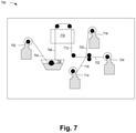
- FIG. 7 illustrates an example assembly line for manufacturing a bi-layer prepreg, according to some embodiments.
- apparatus 700 includes woven fiber roll 702 , woven fiber 704 , resin dip tank 706 , uncured fiber composite 708 , heater 710 , cured fiber composite 712 , thick resin roll 714 , thick resin film 716 , thin resin roll 718 , thin resin film 720 , bi-layer prepreg 722 , and bi-layer prepreg roll 724 . While shown as including rolls of materials, in some embodiments, sheets or sleeves or other configurations may be used.
- woven fiber 704 may correspond with woven fiber layer 102 of prepreg 100 and may comprise fiberglass or carbon fiber or Kevlar, for example.
- resin dip tank 706 may impregnate woven fiber 704 with a resin, such as an epoxy, to form first resin layer 104 and second resin layer 106 , for example, on opposite sides of woven fiber layer 102 .
- resin dip tank 706 may be replaced with sprayers, brushes, or other means of applying resin.
- uncured fiber composite 708 may pass one or more times through heater 710 to cure a thermoset epoxy, forming cured fiber composite 712 .
- thick resin film 716 and thin resin film 720 may correspond to fourth resin layer 110 and third resin layer 108 , respectively, and may be rolled and pressed onto one side of cured fiber composite 712 to form bi-layer prepreg 722 . While shown as being applied as rolled film, in some embodiments, thick resin film 716 and/or thin resin film 720 may be applied by dipping, spraying, or other means. In some embodiments, thick resin film 716 and/or thin resin film 720 may include a covering or supporting layer, such as a polypropylene film or a poly(ethylene terephthalate) (PET) layer that is peeled away from the film prior to being pressed against cured fiber composite 712 .
- PET poly(ethylene terephthalate)
- thick resin film 716 and/or thin resin film 720 may include a covering or supporting layer, that either remains attached to, or is peeled away from, bi-layer prepreg 722 that is rolled into bi-layer prepreg roll 724 .
- FIG. 8 illustrates a flowchart of a method of forming a bi-layer prepreg, in accordance with some embodiments.
- the blocks in the flowchart with reference to FIG. 8 are shown in a particular order, the order of the actions can be modified. Thus, the illustrated embodiments can be performed in a different order, and some actions/blocks may be performed in parallel. Some of the blocks and/or operations listed in FIG. 8 are optional in accordance with certain embodiments. The numbering of the blocks presented is for the sake of clarity and is not intended to prescribe an order of operations in which the various blocks must occur. Additionally, operations from the various flows may be utilized in a variety of combinations.
- Method 800 begins with impregnating ( 802 ) a woven fiber with resin.
- a glass cloth such as woven fiber 704
- resin dip tank 706 to impregnate the woven fiber with uncured resin and create first resin layer 104 and second resin layer 106 on opposite sides of woven fiber layer 102 .
- uncured fiber composite 708 may pass one or more times through heater 710 to cure a thermoset epoxy, forming cured fiber composite 712 .
- a relatively thin resin layer may be added ( 806 ) to one side of the fiber composite.
- the third resin layer 108 may be part of a dielectric build-up film. In some embodiments, the third resin layer 108 may not be required, for example where first resin layer 104 provides adequate dielectric coverage of woven fiber 102 .
- a relatively thick resin layer is added ( 808 ) to the primer layer.
- fourth resin layer 110 may be part of a commercially available dielectric build-up film. In some embodiments, fourth resin layer 110 is semi-cured or semi-solid epoxy resin that has viscosity to fill in voids of an interconnect routing layer.
- the method concludes with rolling ( 810 ) the prepreg for transport.
- a poly(ethylene terephthalate) (PET) layer is included on one or both sides of the prepreg for transport.
- FIG. 9 illustrates a flowchart of a method of forming a device package including a bi-layer prepreg, in accordance with some embodiments.
- the blocks in the flowchart with reference to FIG. 9 are shown in a particular order, the order of the actions can be modified. Thus, the illustrated embodiments can be performed in a different order, and some actions/blocks may be performed in parallel. Some of the blocks and/or operations listed in FIG. 9 are optional in accordance with certain embodiments. The numbering of the blocks presented is for the sake of clarity and is not intended to prescribe an order of operations in which the various blocks must occur. Additionally, operations from the various flows may be utilized in a variety of combinations.
- Method 900 begins with applying ( 902 ) an asymmetrical prepreg to a routing layer of a substrate.
- a bi-layer prepreg 100 is applied to conductive interconnects 202 with fourth resin layer 110 flowing into voids around conductive interconnects 202 .
- fourth resin layer 110 contacts conductive interconnects on a top and two lateral surfaces.
- conductive interconnects 202 extend through fourth resin layer 110 and contact second resin layer 106 on a top surface.
- vias are formed ( 904 ) through the prepreg to couple with conductive features of the routing layer.
- vias 302 are formed by laser drilling or other suitable methods.
- vias 302 include vertical sidewalls that are plated and conductively couple with conductive interconnects 202 .
- build-up layers are formed ( 906 ) over the prepreg.
- upper substrate layers 402 may include multiple layers of prepreg 100 or other dielectric film.
- an integrated circuit device is attached ( 908 ) to the package substrate.
- integrated circuit device 502 may be a single die or a stack of dies.
- solder spheres or other contacts on the package substrate.
- package contacts 602 may represent ball grid array (BGA) contacts.
- the device package may be integrated ( 912 ) into a system, such as being socketed or soldered to a printed circuit board, in some embodiments.
- FIG. 10 illustrates a smart device or a computer system or a SoC (System-on-Chip) 1000 which includes a device package including a bi-layer prepreg, according to some embodiments.
- computing device 1000 represents a mobile computing device, such as a computing tablet, a mobile phone or smart-phone, a wireless-enabled e-reader, or other wireless mobile device. It will be understood that certain components are shown generally, and not all components of such a device are shown in computing device 1000 .
- one or more components of computing device 1000 for example processor 1010 and/or memory subsystem 1060 , are included in a package including a bi-layer prepreg as described above.
- the transistors in various circuits and logic blocks described here are metal oxide semiconductor (MOS) transistors or their derivatives, where the MOS transistors include drain, source, gate, and bulk terminals.
- the transistors and/or the MOS transistor derivatives also include Tri-Gate and FinFET transistors, Gate All Around Cylindrical Transistors, Tunneling FET (TFET), Square Wire, or Rectangular Ribbon Transistors, ferroelectric FET (FeFETs), or other devices implementing transistor functionality like carbon nanotubes or spintronic devices.
- MOSFET symmetrical source and drain terminals i.e., are identical terminals and are interchangeably used here.
- a TFET device on the other hand, has asymmetric Source and Drain terminals.
- Bi-polar junction transistors—BJT PNP/NPN, BiCMOS, CMOS, etc. may be used without departing from the scope of the disclosure.
- computing device 1000 includes a first processor 1010 .
- the various embodiments of the present disclosure may also comprise a network interface within 1070 such as a wireless interface so that a system embodiment may be incorporated into a wireless device, for example, cell phone or personal digital assistant.
- processor 1010 can include one or more physical devices, such as microprocessors, application processors, microcontrollers, programmable logic devices, or other processing means.
- the processing operations performed by processor 1010 include the execution of an operating platform or operating system on which applications and/or device functions are executed.
- the processing operations include operations related to I/O (input/output) with a human user or with other devices, operations related to power management, and/or operations related to connecting the computing device 1000 to another device.
- the processing operations may also include operations related to audio I/O and/or display I/O.
- computing device 1000 includes audio subsystem 1020 , which represents hardware (e.g., audio hardware and audio circuits) and software (e.g., drivers, codecs) components associated with providing audio functions to the computing device. Audio functions can include speaker and/or headphone output, as well as microphone input. Devices for such functions can be integrated into computing device 1000 , or connected to the computing device 1000 . In one embodiment, a user interacts with the computing device 1000 by providing audio commands that are received and processed by processor 1010 .
- audio subsystem 1020 represents hardware (e.g., audio hardware and audio circuits) and software (e.g., drivers, codecs) components associated with providing audio functions to the computing device. Audio functions can include speaker and/or headphone output, as well as microphone input. Devices for such functions can be integrated into computing device 1000 , or connected to the computing device 1000 . In one embodiment, a user interacts with the computing device 1000 by providing audio commands that are received and processed by processor 1010 .
- Display subsystem 1030 represents hardware (e.g., display devices) and software (e.g., drivers) components that provide a visual and/or tactile display for a user to interact with the computing device 1000 .
- Display subsystem 1030 includes display interface 1032 , which includes the particular screen or hardware device used to provide a display to a user.
- display interface 1032 includes logic separate from processor 1010 to perform at least some processing related to the display.
- display subsystem 1030 includes a touch screen (or touch pad) device that provides both output and input to a user.
- I/O controller 1040 represents hardware devices and software components related to interaction with a user. I/O controller 1040 is operable to manage hardware that is part of audio subsystem 1020 and/or display subsystem 1030 . Additionally, I/O controller 1040 illustrates a connection point for additional devices that connect to computing device 1000 through which a user might interact with the system. For example, devices that can be attached to the computing device 1000 might include microphone devices, speaker or stereo systems, video systems or other display devices, keyboard or keypad devices, or other I/O devices for use with specific applications such as card readers or other devices.
- I/O controller 1040 can interact with audio subsystem 1020 and/or display subsystem 1030 .
- input through a microphone or other audio device can provide input or commands for one or more applications or functions of the computing device 1000 .
- audio output can be provided instead of, or in addition to display output.
- display subsystem 1030 includes a touch screen
- the display device also acts as an input device, which can be at least partially managed by I/O controller 1040 .
- I/O controller 1040 manages devices such as accelerometers, cameras, light sensors or other environmental sensors, or other hardware that can be included in the computing device 1000 .
- the input can be part of direct user interaction, as well as providing environmental input to the system to influence its operations (such as filtering for noise, adjusting displays for brightness detection, applying a flash for a camera, or other features).
- computing device 1000 includes power management 1050 that manages battery power usage, charging of the battery, and features related to power saving operation.
- Memory subsystem 1060 includes memory devices for storing information in computing device 1000 . Memory can include nonvolatile (state does not change if power to the memory device is interrupted) and/or volatile (state is indeterminate if power to the memory device is interrupted) memory devices. Memory subsystem 1060 can store application data, user data, music, photos, documents, or other data, as well as system data (whether long-term or temporary) related to the execution of the applications and functions of the computing device 1000 .
- Elements of embodiments are also provided as a machine-readable medium (e.g., memory 1060 ) for storing the computer-executable instructions.
- the machine-readable medium e.g., memory 1060
- PCM phase change memory
- embodiments of the disclosure may be downloaded as a computer program (e.g., BIOS) which may be transferred from a remote computer (e.g., a server) to a requesting computer (e.g., a client) by way of data signals via a communication link (e.g., a modem or network connection).
- BIOS a computer program
- a remote computer e.g., a server
- a requesting computer e.g., a client
- a communication link e.g., a modem or network connection
- Connectivity 1070 includes hardware devices (e.g., wireless and/or wired connectors and communication hardware) and software components (e.g., drivers, protocol stacks) to enable the computing device 1000 to communicate with external devices.
- the computing device 1000 could be separate devices, such as other computing devices, wireless access points or base stations, as well as peripherals such as headsets, printers, or other devices.
- Connectivity 1070 can include multiple different types of connectivity.
- the computing device 1000 is illustrated with cellular connectivity 1072 and wireless connectivity 1074 .
- Cellular connectivity 1072 refers generally to cellular network connectivity provided by wireless carriers, such as provided via GSM (global system for mobile communications) or variations or derivatives, CDMA (code division multiple access) or variations or derivatives, TDM (time division multiplexing) or variations or derivatives, or other cellular service standards.
- Wireless connectivity (or wireless interface) 1074 refers to wireless connectivity that is not cellular, and can include personal area networks (such as Bluetooth, Near Field, etc.), local area networks (such as Wi-Fi), and/or wide area networks (such as WiMax), or other wireless communication.
- Peripheral connections 1080 include hardware interfaces and connectors, as well as software components (e.g., drivers, protocol stacks) to make peripheral connections. It will be understood that the computing device 1000 could both be a peripheral device (“to” 1082 ) to other computing devices, as well as have peripheral devices (“from” 1084 ) connected to it.
- the computing device 1000 commonly has a “docking” connector to connect to other computing devices for purposes such as managing (e.g., downloading and/or uploading, changing, synchronizing) content on computing device 1000 .
- a docking connector can allow computing device 1000 to connect to certain peripherals that allow the computing device 1000 to control content output, for example, to audiovisual or other systems.
- the computing device 1000 can make peripheral connections 1080 via common or standards-based connectors.
- Common types can include a Universal Serial Bus (USB) connector (which can include any of a number of different hardware interfaces), DisplayPort including MiniDisplayPort (MDP), High Definition Multimedia Interface (HDMI), Firewire, or other types.
- USB Universal Serial Bus
- MDP MiniDisplayPort
- HDMI High Definition Multimedia Interface
- Firewire or other types.
- first embodiment may be combined with a second embodiment anywhere the particular features, structures, functions, or characteristics associated with the two embodiments are not mutually exclusive.
- an apparatus comprising: a fiber layer, a first resin layer on a first surface of the fiber layer, a second resin layer on a second surface of the fiber layer, the second surface opposite the first surface, and the first and the second resin layers comprising cured resin, a third resin layer on the first resin layer, and a fourth resin layer on the second resin layer, the third and the fourth resin layers comprising an uncured resin, and wherein the fourth resin layer has a thickness greater than a thickness of the third resin layer.
- the thickness of the fourth resin layer is at least twice the thickness of the third resin layer. In some embodiments, the thickness of the third resin layer is less than 5 um, and wherein the thickness of the fourth resin layer is greater than 10 um. Some embodiments also include a layer of polyethylene terephthalate (PET) on the third or fourth resin layers. In some embodiments, the third and the fourth resin layers comprise a semi-cured resin. Some embodiments also include the fourth resin layer on a metal feature of a substrate. In some embodiments, the fiber layer comprises a #1010 weave fiberglass. In some embodiments, the third and the fourth resin layers comprise a pre-formed film comprising epoxy with silica-based filler particles.
- PET polyethylene terephthalate
- an integrated circuit package comprising: a substrate comprising: a fiber layer, a first resin layer on a first surface of the fiber layer, a second resin layer on a second surface of the fiber layer, the second surface opposite the first surface, and the first and the second resin layers comprising an epoxy resin, a third resin layer on the first resin layer, a fourth resin layer on the second resin layer, the fourth resin layer having a thickness greater than the third resin layer, a conductive interconnect on a substrate surface, the conductive interconnect contacting the fourth resin layer on two or more sides, and a via through the fiber, the first, the second, the third, and the fourth resin layers, the via coupled with the conductive interconnect, and one or more integrated circuit die(s) coupled with the substrate.
- the first and the second resin layers each have a thickness less than a height of the conductive interconnect, and wherein the height of the conductive interconnect is less than 10 um.
- the thickness of the fourth resin layer is at least twice the thickness of the third resin layer.
- the fiber, the first, the second, the third, and the fourth resin layers have a total thickness of less than 40 um.
- the first, the second, the third, and the fourth resin layers comprise a thermoset epoxy resin with silica-based filler particles.
- the fiber comprises a #1010 weave fiberglass.
- a system comprising: a display subsystem, a wireless communication interface, and an integrated circuit package, the integrated circuit package comprising: a substrate comprising: a fiber layer, a first resin layer on a first surface of the fiber layer, a second resin layer on a second surface of the fiber layer, the second surface opposite the first surface, and the first and the second resin layers comprising an epoxy resin, a third resin layer on the first resin layer, a fourth resin layer on the second resin layer, the fourth resin layer having a thickness greater than the third resin layer, a conductive interconnect on a substrate surface, the conductive interconnect contacting the fourth resin layer on two or more sides, and a via through the fiber, the first resin, the second resin, the third resin, and the fourth resin layers, the via coupled with the conductive interconnect, and one or more integrated circuit die(s) coupled with the substrate.
- the thickness of the fourth resin layer is at least twice the thickness of the third resin layer. In some embodiments, the thickness of the third resin layer is less than 5 um, and wherein the thickness of the fourth resin layer is greater than 10 um. Some embodiments also include the fiber, the first resin, the second resin, the third resin, and the fourth resin layers having a total thickness of less than 40 um. In some embodiments, the first, the second, the third, and the fourth resin layers comprise a thermoset epoxy resin with silica-based filler particles. In some embodiments, the fiber layer comprises a #1010 weave fiberglass.
- a method of forming a bi-layer prepreg comprising: impregnating a fiber with resin, forming a first resin layer on a first side of the fiber, wherein the first resin layer has a thickness less than a thickness of the fiber, and forming a second resin layer on a second side of the fiber, the second side of the fiber is opposite the first side of the fiber, and wherein the second resin layer has a thickness greater than the thickness of the fiber.
- impregnating the fiber with resin comprises: dipping the fiber in a liquid epoxy, and heating the fiber composite.
- the liquid epoxy comprises an epoxy resin with silica-based filler particles.
- forming the second resin layer comprises: peeling a cover layer off a build-up film to expose a resin layer, applying the resin layer of the build-up film to the second side of the impregnated fiber, and pressing the build-up film against the impregnated fiber with mechanical rollers.
- Some embodiments also include rolling the bi-layer prepreg on a spool.
- the fiber comprises fiberglass fabric.
- a method of forming a device package with a bi-layer prepreg comprising: receiving a coreless substrate having a conductive interconnect over a dielectric surface, and applying a bi-layer prepreg over the coreless substrate, wherein the bi-layer prepreg comprises: a fiber layer, a first resin layer on a first surface of the fiber layer, a second resin layer on a second surface of the fiber layer, the second surface opposite the first surface, and the first and the second resin layers comprising cured resin, a third resin layer on the first resin layer, and a fourth resin layer on the second resin layer, the third and the fourth resin layers comprising an uncured resin, and wherein the fourth resin layer has a thickness greater than a thickness of the third resin layer, wherein applying the bi-layer prepreg over the coreless substrate comprises placing the fourth resin layer in contact with the conductive interconnect.
- Some embodiments also include forming a via through the bi-layer prepreg coupled with the conductive interconnect. Some embodiments also include forming build-up layers over the bi-layer prepreg that couple the via with a package substrate contact. Some embodiments also include coupling an integrated circuit device with the package substrate contact.
- the third and fourth resin layers comprise an epoxy resin with silica-based filler particles.
- the fiber layer comprises fiberglass fabric.
Landscapes
- Engineering & Computer Science (AREA)
- Microelectronics & Electronic Packaging (AREA)
- Physics & Mathematics (AREA)
- General Physics & Mathematics (AREA)
- Condensed Matter Physics & Semiconductors (AREA)
- Computer Hardware Design (AREA)
- Power Engineering (AREA)
- Manufacturing & Machinery (AREA)
- Textile Engineering (AREA)
- Geometry (AREA)
- Ceramic Engineering (AREA)
- Optics & Photonics (AREA)
- Production Of Multi-Layered Print Wiring Board (AREA)
Abstract
Description
Claims (19)
Priority Applications (1)
| Application Number | Priority Date | Filing Date | Title |
|---|---|---|---|
| US15/967,122 US11276618B2 (en) | 2018-04-30 | 2018-04-30 | Bi-layer prepreg for reduced dielectric thickness |
Applications Claiming Priority (1)
| Application Number | Priority Date | Filing Date | Title |
|---|---|---|---|
| US15/967,122 US11276618B2 (en) | 2018-04-30 | 2018-04-30 | Bi-layer prepreg for reduced dielectric thickness |
Publications (2)
| Publication Number | Publication Date |
|---|---|
| US20190333832A1 US20190333832A1 (en) | 2019-10-31 |
| US11276618B2 true US11276618B2 (en) | 2022-03-15 |
Family
ID=68292827
Family Applications (1)
| Application Number | Title | Priority Date | Filing Date |
|---|---|---|---|
| US15/967,122 Active 2040-07-13 US11276618B2 (en) | 2018-04-30 | 2018-04-30 | Bi-layer prepreg for reduced dielectric thickness |
Country Status (1)
| Country | Link |
|---|---|
| US (1) | US11276618B2 (en) |
Families Citing this family (4)
| Publication number | Priority date | Publication date | Assignee | Title |
|---|---|---|---|---|
| US11064615B2 (en) * | 2019-09-30 | 2021-07-13 | Texas Instruments Incorporated | Wafer level bump stack for chip scale package |
| JP7669253B2 (en) | 2021-11-17 | 2025-04-28 | 株式会社アイシン | Displacer for refrigerator and method for manufacturing the same |
| WO2023171403A1 (en) * | 2022-03-07 | 2023-09-14 | パナソニックIpマネジメント株式会社 | Printed circuit board having built-in thick conductor and method for manufacturing same |
| WO2025088489A1 (en) * | 2023-10-25 | 2025-05-01 | Bcomp Sa | Fibre reinforced polymer composite sheet with moisture barrier surface layer, multilayer composite material with said sheet, composite product with said material and manufacturing method of said sheet |
Citations (8)
| Publication number | Priority date | Publication date | Assignee | Title |
|---|---|---|---|---|
| US5588207A (en) * | 1992-09-22 | 1996-12-31 | Matsushita Electric Industrial Co., Ltd. | Method of manufacturing two-sided and multi-layered printed circuit boards |
| US6078229A (en) * | 1997-08-05 | 2000-06-20 | Nec Corporation | Surface acoustic wave device mounted with a resin film and method of making same |
| US20030063453A1 (en) * | 2001-09-28 | 2003-04-03 | Fujitsu Limited | Multilayer wiring circuit board |
| US6570099B1 (en) * | 1999-11-09 | 2003-05-27 | Matsushita Electric Industrial Co., Ltd. | Thermal conductive substrate and the method for manufacturing the same |
| US20050186768A1 (en) * | 2000-02-09 | 2005-08-25 | Matsushita Electric Industrial Co., Ltd. | Wiring substrate produced by transfer material method |
| US20140360765A1 (en) * | 2013-06-10 | 2014-12-11 | Shinko Electric Industries Co., Ltd. | Wiring substrate and manufacturing method of wiring substrate |
| US20160020165A1 (en) * | 2014-05-06 | 2016-01-21 | Intel Corporation | Multi-layer package with integrated antenna |
| US20170358700A1 (en) * | 2011-06-06 | 2017-12-14 | Dsm Ip Assets B.V. | Metal foil pattern layered body, metal foil layered body, metal foil multi-layer substrate, solar cell module, and method of manufacturing metal foil pattern layered body |
-
2018
- 2018-04-30 US US15/967,122 patent/US11276618B2/en active Active
Patent Citations (9)
| Publication number | Priority date | Publication date | Assignee | Title |
|---|---|---|---|---|
| US5588207A (en) * | 1992-09-22 | 1996-12-31 | Matsushita Electric Industrial Co., Ltd. | Method of manufacturing two-sided and multi-layered printed circuit boards |
| US6078229A (en) * | 1997-08-05 | 2000-06-20 | Nec Corporation | Surface acoustic wave device mounted with a resin film and method of making same |
| US6570099B1 (en) * | 1999-11-09 | 2003-05-27 | Matsushita Electric Industrial Co., Ltd. | Thermal conductive substrate and the method for manufacturing the same |
| US20050186768A1 (en) * | 2000-02-09 | 2005-08-25 | Matsushita Electric Industrial Co., Ltd. | Wiring substrate produced by transfer material method |
| US20030063453A1 (en) * | 2001-09-28 | 2003-04-03 | Fujitsu Limited | Multilayer wiring circuit board |
| US7253023B2 (en) * | 2001-09-28 | 2007-08-07 | Fujitsu Limited | Multilayer wiring circuit board |
| US20170358700A1 (en) * | 2011-06-06 | 2017-12-14 | Dsm Ip Assets B.V. | Metal foil pattern layered body, metal foil layered body, metal foil multi-layer substrate, solar cell module, and method of manufacturing metal foil pattern layered body |
| US20140360765A1 (en) * | 2013-06-10 | 2014-12-11 | Shinko Electric Industries Co., Ltd. | Wiring substrate and manufacturing method of wiring substrate |
| US20160020165A1 (en) * | 2014-05-06 | 2016-01-21 | Intel Corporation | Multi-layer package with integrated antenna |
Also Published As
| Publication number | Publication date |
|---|---|
| US20190333832A1 (en) | 2019-10-31 |
Similar Documents
| Publication | Publication Date | Title |
|---|---|---|
| US12327773B2 (en) | Package with underfill containment barrier | |
| US11276618B2 (en) | Bi-layer prepreg for reduced dielectric thickness | |
| US10880994B2 (en) | Top-side connector interface for processor packaging | |
| US20190006264A1 (en) | Embedded bridge with through-silicon vias | |
| KR102613403B1 (en) | Patch accommodating embedded dies with different thicknesses | |
| US9773752B2 (en) | Printed circuit boards and semiconductor packages including the same | |
| US20180352649A1 (en) | Connector interface for processor packaging | |
| US11705377B2 (en) | Stacked die cavity package | |
| US20190287956A1 (en) | Recessed semiconductor die in a die stack to accomodate a component | |
| US20230411385A1 (en) | Package with embedded capacitors | |
| US20190109122A1 (en) | Electronic packages with stacked sitffeners and methods of assembling same | |
| US20190311983A1 (en) | Stacking multiple dies having dissimilar interconnect structure layout and pitch | |
| US10410940B2 (en) | Semiconductor package with cavity | |
| US11887932B2 (en) | Dielectric-filled trench isolation of vias | |
| US11158568B2 (en) | Package with wall-side capacitors | |
| US11574874B2 (en) | Package architecture utilizing photoimageable dielectric (PID) for reduced bump pitch | |
| US20190206786A1 (en) | Thin film passive devices integrated in a package substrate | |
| US11075260B2 (en) | Substrate comprising recessed interconnects and a surface mounted passive component | |
| US20210287975A1 (en) | Landing pad apparatus for through-silicon-vias | |
| US11282633B2 (en) | Device with out-plane inductors | |
| US20250112198A1 (en) | In-cavity epoxy placement for package reliability | |
| US11037916B2 (en) | Apparatus with multi-wafer based device comprising embedded active devices and method for forming such | |
| US20240222345A1 (en) | Die attach in glass core package through organic-to-organic bonding | |
| US20250112085A1 (en) | Apparatus and methods for capillary underfill of embedded devices | |
| US20240213235A1 (en) | Architectures for backside power delivery with stacked integrated circuit devices |
Legal Events
| Date | Code | Title | Description |
|---|---|---|---|
| AS | Assignment |
Owner name: INTEL CORPORATION, CALIFORNIA Free format text: ASSIGNMENT OF ASSIGNORS INTEREST;ASSIGNORS:ROSCH, JONATHAN;BROWN, ANDREW J.;REEL/FRAME:045673/0216 Effective date: 20180426 |
|
| FEPP | Fee payment procedure |
Free format text: ENTITY STATUS SET TO UNDISCOUNTED (ORIGINAL EVENT CODE: BIG.); ENTITY STATUS OF PATENT OWNER: LARGE ENTITY |
|
| STPP | Information on status: patent application and granting procedure in general |
Free format text: DOCKETED NEW CASE - READY FOR EXAMINATION |
|
| STPP | Information on status: patent application and granting procedure in general |
Free format text: NON FINAL ACTION MAILED |
|
| STPP | Information on status: patent application and granting procedure in general |
Free format text: RESPONSE TO NON-FINAL OFFICE ACTION ENTERED AND FORWARDED TO EXAMINER |
|
| STPP | Information on status: patent application and granting procedure in general |
Free format text: NOTICE OF ALLOWANCE MAILED -- APPLICATION RECEIVED IN OFFICE OF PUBLICATIONS |
|
| STCF | Information on status: patent grant |
Free format text: PATENTED CASE |
|
| MAFP | Maintenance fee payment |
Free format text: PAYMENT OF MAINTENANCE FEE, 4TH YEAR, LARGE ENTITY (ORIGINAL EVENT CODE: M1551); ENTITY STATUS OF PATENT OWNER: LARGE ENTITY Year of fee payment: 4 |