US11275876B2 - Program, information processing device, and information processing method - Google Patents
Program, information processing device, and information processing method Download PDFInfo
- Publication number
- US11275876B2 US11275876B2 US16/400,872 US201916400872A US11275876B2 US 11275876 B2 US11275876 B2 US 11275876B2 US 201916400872 A US201916400872 A US 201916400872A US 11275876 B2 US11275876 B2 US 11275876B2
- Authority
- US
- United States
- Prior art keywords
- blocks
- clock frequency
- block
- conversion
- series
- Prior art date
- Legal status (The legal status is an assumption and is not a legal conclusion. Google has not performed a legal analysis and makes no representation as to the accuracy of the status listed.)
- Active, expires
Links
Images


Classifications
-
- G—PHYSICS
- G06—COMPUTING OR CALCULATING; COUNTING
- G06F—ELECTRIC DIGITAL DATA PROCESSING
- G06F30/00—Computer-aided design [CAD]
- G06F30/20—Design optimisation, verification or simulation
-
- G—PHYSICS
- G06—COMPUTING OR CALCULATING; COUNTING
- G06F—ELECTRIC DIGITAL DATA PROCESSING
- G06F1/00—Details not covered by groups G06F3/00 - G06F13/00 and G06F21/00
- G06F1/26—Power supply means, e.g. regulation thereof
- G06F1/32—Means for saving power
- G06F1/3203—Power management, i.e. event-based initiation of a power-saving mode
- G06F1/3234—Power saving characterised by the action undertaken
- G06F1/324—Power saving characterised by the action undertaken by lowering clock frequency
-
- G—PHYSICS
- G06—COMPUTING OR CALCULATING; COUNTING
- G06F—ELECTRIC DIGITAL DATA PROCESSING
- G06F1/00—Details not covered by groups G06F3/00 - G06F13/00 and G06F21/00
- G06F1/04—Generating or distributing clock signals or signals derived directly therefrom
- G06F1/08—Clock generators with changeable or programmable clock frequency
-
- G—PHYSICS
- G06—COMPUTING OR CALCULATING; COUNTING
- G06F—ELECTRIC DIGITAL DATA PROCESSING
- G06F1/00—Details not covered by groups G06F3/00 - G06F13/00 and G06F21/00
- G06F1/26—Power supply means, e.g. regulation thereof
- G06F1/32—Means for saving power
- G06F1/3203—Power management, i.e. event-based initiation of a power-saving mode
- G06F1/3206—Monitoring of events, devices or parameters that trigger a change in power modality
-
- Y—GENERAL TAGGING OF NEW TECHNOLOGICAL DEVELOPMENTS; GENERAL TAGGING OF CROSS-SECTIONAL TECHNOLOGIES SPANNING OVER SEVERAL SECTIONS OF THE IPC; TECHNICAL SUBJECTS COVERED BY FORMER USPC CROSS-REFERENCE ART COLLECTIONS [XRACs] AND DIGESTS
- Y02—TECHNOLOGIES OR APPLICATIONS FOR MITIGATION OR ADAPTATION AGAINST CLIMATE CHANGE
- Y02D—CLIMATE CHANGE MITIGATION TECHNOLOGIES IN INFORMATION AND COMMUNICATION TECHNOLOGIES [ICT], I.E. INFORMATION AND COMMUNICATION TECHNOLOGIES AIMING AT THE REDUCTION OF THEIR OWN ENERGY USE
- Y02D10/00—Energy efficient computing, e.g. low power processors, power management or thermal management
Definitions
- the disclosure relates to a program, an information processing device, and an information processing method, and to, for example, a program, an information processing device, and an information processing method used in a simulation of a model in model base development.
- a system is developed using a process of a V model in some cases in system development.
- the development is advanced in such a manner that in a process before a coding process, a developer creates a document, an expert reviews the same, and the reviewed result is input in the next process.
- Japanese Unexamined Patent Application Publication No. 2008-215254 discloses a simplifying method in model base development in which a particular simple model base different from a detailed model base is mounted in a vehicle ECU (engine control unit) for engine control.
- a vehicle ECU engine control unit
- an adaptive value for adapting the simple model base to an actual machine is calculated backward in the simple model base, and a value necessary to calculate the adaptive value backward is calculated by the detailed model base.
- the development is advanced in such a manner that a model configured using a plurality of blocks is created in each process, a simulation of the model is performed, and the behavior and performance are estimated.
- the simulation of the model can estimate the behavior and performance of the system more accurately than a theoretical simple calculation.
- a failure pattern that hardly or cannot occur in an actual system can be also reproduced.
- a program is executed in an information processing device including a processor and a memory.
- the program allows the processor to execute a step of, on the basis of a simulation result of a model in the case where a series of blocks having an input block, one or more operation blocks, and an output block are allowed to operate at a predetermined clock frequency, deciding a new clock frequency of a target block that is allowed to operate at a clock frequency lower than the predetermined clock frequency.
- the program allows the processor to further execute a step of setting the conversion ratios of conversion blocks so as to execute a simulation of the model in which the target block is allowed to operate at the new clock frequency lower than the predetermined clock frequency and the remaining blocks are allowed to operate at the predetermined clock frequency.
- An information processing device includes a processor and a memory.
- the processor decides a new clock frequency of a target block that is allowed to operate at a clock frequency lower than the predetermined clock frequency.
- the processor sets the conversion ratios of conversion blocks arranged among the blocks so as to execute a simulation of the model in which the target block is allowed to operate at the new clock frequency lower than the predetermined clock frequency and the remaining blocks are allowed to operate at the predetermined clock frequency.
- An information processing method is executed by a processor of an information processing device.
- the information processing method includes a step of, on the basis of a simulation result of a model in the case where a series of blocks having an input block, one or more operation blocks, and an output block are allowed to operate at a predetermined clock frequency, deciding a new clock frequency of a target block that is allowed to operate at a clock frequency lower than the predetermined clock frequency.
- the information processing method further includes a step of setting the conversion ratios of conversion blocks so as to execute a simulation of the model in which the target block is allowed to operate at the new clock frequency lower than the predetermined clock frequency and the remaining blocks are allowed to operate at the predetermined clock frequency.
- the simulation time can be easily reduced in model base development.
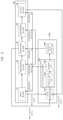
- FIG. 1 is a diagram for explaining a hardware configuration and an operation outline of an information processing device according to an embodiment
- FIG. 2 is a diagram for showing an example of a model according to the embodiment
- FIG. 3 is a block diagram for showing an example of a functional configuration of an improvement program according to a first embodiment
- FIG. 4 is a diagram for explaining a calculation method by a number-of-times calculation unit according to the first embodiment
- FIG. 5 is a diagram for explaining a reason of reduction in simulation time
- FIG. 6 is a flowchart for showing an example of a processing procedure of a processor according to the first embodiment
- FIG. 7 is a block diagram for showing an example of a functional configuration of an improvement program according to a second embodiment
- FIG. 8 is a flowchart for showing an example of a processing procedure of a processor according to the second embodiment
- FIG. 9 is a block diagram for showing an example of a functional configuration of an improvement program according to a third embodiment.
- FIGS. 10A and 10B are diagrams each explaining a calculation method of an output fluctuation rate according to the third embodiment.
- FIG. 11 is a flowchart for showing an example of a processing procedure of a processor according to the third embodiment.
- FIG. 1 is a diagram for explaining a hardware configuration and an operation outline of an information processing device 100 according to an embodiment.
- the information processing device 100 includes a processor 102 , an auxiliary storage device 120 , and a main storage device 110 .
- the information processing device 100 may be configured to include various input devices (for example, a keyboard, buttons, and a mouse) for accepting an operation input to the information processing device 100 , a display for displaying various information, and a communication interface for communicating various data.
- various input devices for example, a keyboard, buttons, and a mouse
- the information processing device 100 is, for example, a stationary personal computer including a display.
- the information processing device 100 is not limited to this, but may be a device having an operation function to be described later such as a laptop personal computer.
- the processor 102 is typically an operation processing unit such as a CPU (Central Processing Unit).
- the processor 102 reads an OS (Operating System) and various programs including application programs installed in the auxiliary storage device 120 , and executes the same while being expanded to the main storage device 110 .
- OS Operating System
- the main storage device 110 is typically a volatile storage medium such as a DRAM (Dynamic Random Access Memory), and holds various work data necessary to execute various programs in addition to codes of various programs including an OS executed by the processor 102 .
- the auxiliary storage device 120 is a non-volatile storage medium such as a hard disk or an SSD (Solid State Drive), and holds various design information in addition to various programs including an OS. It should be noted that the main storage device 110 and the auxiliary storage device 120 will be collectively referred to as a memory in the following description in some cases.
- the auxiliary storage device 120 stores a simulation execution environment program (hereinafter, also simply referred to as an “execution environment program”) 112 , a simulation target model (hereinafter, also simply referred to as a “model”) 114 , and a simulation time improvement program (hereinafter, also simply referred to as an “improvement program”) 116 .
- execution environment program hereinafter, also simply referred to as an “execution environment program”
- model simulation target model
- improvement program hereinafter, also simply referred to as an “improvement program”
- the execution environment program 112 is a program for providing an execution environment of a simulation used for model base development, and is, for example, Simulink (registered trademark) that operates on MATLAB (registered trademark) of The MathWorks, Inc. (registered trademark).
- a developer describes a model 114 of a target program using the execution environment program 112 .
- the model 114 is described as a function unit called “block” and a combination of connections representing an input/output relation between the function units.
- FIG. 2 is a diagram for showing an example of the model 114 according to the embodiment.
- the model 114 includes an input block 11 , conversion blocks 12 A to 12 E, operation blocks 13 A to 13 C, and output blocks 14 A and 14 B.
- the model 114 is an assembly obtained by connecting these blocks using the connections representing an input/output relation.
- a conversion block 12 when explaining a configuration and a function common to each of the conversion blocks 12 A to 12 E, these are collectively referred to as a conversion block 12 .
- an operation block 13 When explaining a configuration and a function common to each of the operation blocks 13 A to 13 C, these are collectively referred to as an operation block 13 .
- an output block 14 When explaining a configuration and a function common to each of the output blocks 14 A and 14 B, these are collectively referred to as an output block 14 .
- the input block 11 is a block that accepts an input of data from the outside of the model and outputs the data. For example, the input block 11 reads a file from the outside, and outputs the read value.
- the conversion block 12 converts a clock frequency with a set conversion ratio. Specifically, the conversion block 12 converts a clock frequency that operates the block coupled to the input side of the conversion block 12 with a set conversion ratio, and outputs the converted frequency.
- the conversion ratio of the conversion block 12 A is set to “2”.
- the clock frequency of the block coupled to the output side of the conversion block 12 to the clock frequency of the block coupled to the input side of the conversion block 12 is set as the conversion ratio of the conversion block 12 .
- the operation block 13 executes a predetermined operation for input data, and outputs the result.
- the operation block 13 executes four arithmetic operations for an input value, and outputs the result.
- the operation block 13 outputs 100 if an input value is within a preliminarily-set range (for example, 1 ⁇ input value ⁇ 10), and outputs an input value as it is if the input value is out of the preliminarily-set range.
- the operation block 13 executes an integration process of an input value, and outputs the integration result.
- the output block 14 is a block that outputs input data to the outside of the model. For example, the output block 14 executes writing to a file or outputs the waveform of voltage (or a current).
- the conversion blocks 12 are arranged among the blocks of the series of blocks.
- the model 114 has a processing route including a series of blocks including the input block 11 , the operation block 13 A, and the output block 14 A and the conversion blocks 12 A and 12 B arranged among the blocks of the series of blocks.
- the model 114 has a processing route including a series of blocks including the input block 11 , the operation blocks 13 B and 13 C, and the output block 14 B and the conversion blocks 12 C to 12 E arranged among the blocks of the series of blocks.
- FIG. 1 An operation outline of the information processing device 100 according to the embodiment will be described with reference to FIG. 1 again.
- main processes in the information processing device 100 there are five processes such as a program reading process (1), a simulation execution process (2), a simulation result acquisition process (3), a clock frequency decision process (4), and a simulation re-execution process (5).
- the numbers in parentheses of FIG. 1 correspond to the above processes.
- the processor 102 reads the execution environment program 112 , the model 114 , and the improvement program 116 from the auxiliary storage device 120 , and loads the same to the main storage device 110 .
- the processor 102 allows a series of blocks to operate at a predetermined clock frequency by executing the execution environment program 112 , and executes a simulation of the model 114 .
- the conversion ratio of each conversion block 12 is set to “1” (namely, the frequency conversion is not performed).
- the processor 102 executes the improvement program 116 , and acquires the simulation result.
- the processor 102 executes the improvement program 116 , and decides the optimum clock frequency for each of the series of blocks on the basis of the acquired simulation result. Specifically, the processor 102 analyzes the degree of reduction in the present clock frequency of each of the series of blocks within a range where the simulation result is not substantially affected on the basis of the simulation result, and decides the clock frequency of each block on the basis of the analysis result. In addition, the processor 102 sets the conversion ratio of each conversion block 12 arranged between the blocks on the basis of the clock frequency of each of the decided blocks.
- the processor 102 re-executes the execution environment program 112 to execute a simulation of the model 114 with the clock frequency of each block changed.
- the simulation time in the simulation re-execution process becomes shorter than that in the simulation execution process.
- the clock frequency of each block is reduced within a range where the simulation result is not substantially affected, and thus the accuracy of the simulation result can be also secured. Accordingly, the simulation time can be easily reduced by using the improvement program 116 while securing the accuracy of the simulation result.
- FIG. 3 is a block diagram for showing an example of a functional configuration of an improvement program 116 A according to a first embodiment.
- an information processing device 100 includes a data acquisition unit 31 A, a clock frequency decision unit 32 A, and a conversion ratio setting unit 35 A.
- the improvement program 116 A corresponds to the improvement program 116 shown in FIG. 1
- an additional sign “A” is attached for convenience sake to be distinguished from other embodiments. This also applies to second and third embodiments.
- a model 20 loaded to a main storage device 110 includes an input block 21 , conversion blocks 22 and 24 , an operation block 23 , and an output block 25 .
- the model 20 corresponds to the model 114 shown in FIG. 1 , a case in which one input block, one operation block, and one output block are provided will be described in order to simplify the explanation.
- a data acquisition unit 31 A acquires a simulation result of the model 20 in the case where a series of blocks including an input block 21 , an operation block 23 , and an output block 25 (hereinafter, also simply referred to as “a series of blocks”) are allowed to operate at a predetermined clock frequency Fs (for example, 100 Hz).
- the predetermined clock frequency Fs is a frequency preliminarily set by a user with reference to the specifications and the like.
- the data acquisition unit 31 A acquires input/output data of each of the input block 21 , the operation block 23 , and the output block 25 . Each input/output data is output to the clock frequency decision unit 32 A.
- the clock frequency decision unit 32 A decides a new clock frequency of a target block allowed to operate at a clock frequency lower than the predetermined clock frequency Fs among a series of blocks on the basis of the acquired input/output data.
- the clock frequency decision unit 32 A includes a number-of-times calculation unit 33 A and a decision unit 34 A.
- the number-of-times calculation unit 33 A calculates the number of continuous times of the same input/output data (hereinafter, also simply referred to as “the number of continuous times”) for each of a series of blocks by analyzing each input/output data.
- the calculation method by the number-of-times calculation unit will be concretely described using FIG. 4 .
- FIG. 4 is a diagram for explaining the calculation method by the number-of-times calculation unit according to the first embodiment.
- the conversion blocks are not illustrated in order to easily understand the drawing because the conversion ratio of each of the conversion blocks 22 and 24 is “1”. It should be noted that the input value and the output value of a block are expressed in the form of (input value, output value) in the following description.
- the input/output values of the input block 21 are (1, 1), the input/output values of the operation block 23 are (1, 2), and the input/output values of the output block 25 are (2, 2) in the 0-th clock.
- the input/output values of the input block 21 are (1, 1), the input/output values of the operation block 23 are (1, 3), and the input/output values of the output block 25 are (3, 3) in the first clock.
- the input/output values of the input block 21 are the same between the 0-th clock and the first clock.
- a case in which the input/output values of the input block 21 are changed to (2, 2) in the second clock and (2, 2) in the third clock namely, a case in which the input/output values are the same between the 2n-th (n is an integer of 0 or larger) clock and the (2n+1)-th clock will be assumed.
- the number-of-times calculation unit 33 A calculates the number of continuous times of the same input/output data as “2” for the input block 21 .
- the input/output data of the operation block 23 and the output block 25 are different from each other between the 0-th clock and the first clock.
- the number-of-times calculation unit 33 A calculates the number of continuous times of the same input/output data as “1” for each of the operation block 23 and the output block 25 .
- the decision unit 34 A selects a target block allowed to operate at a clock frequency lower than the predetermined clock frequency Fs on the basis of the predetermined clock frequency Fs and the number of continuous times for each of a series of blocks, and decides the clock frequency of the selected target block.
- the clock frequency of the target block is a value obtained by dividing the predetermined clock frequency Fs by the number of continuous times for the target block.
- the decision unit 34 A selects a block having “2” or larger of the number of continuous times as a target block.
- the decision unit 34 A decides 1 ⁇ 2 of the predetermined clock frequency Fs as the clock frequency of the input block 21 .
- the decision unit 34 A decides a value obtained by dividing the predetermined clock frequency Fs (for example, 100 Hz) by the number of continuous times (for example, 2) as the new clock frequency (for example, 50 Hz) of the target block (for example, the input block 21 ).
- the decision unit 34 A decides the predetermined clock frequency Fs as the clock frequency of each of the operation block 23 and the output block 25 . As described above, the present clock frequency is maintained for each block other than the target block without setting a new clock frequency.
- the decision unit 34 A outputs the decided clock frequency to each of a series of blocks. Specifically, the decision unit 34 A outputs a clock frequency f 1 to the input block 21 , outputs a clock frequency f 2 to the operation block 23 , and outputs a clock frequency f 3 to the output block 25 .
- the clock frequencies f 1 , f 2 , and f 3 are Fs/2, Fs, and Fs, respectively.
- the conversion ratio setting unit 35 A sets the conversion ratio of each of the conversion blocks 22 and 24 in order to allow each of a series of blocks to appropriately operate at the clock frequency decided by the decision unit 34 . Specifically, the conversion ratio setting unit 35 A sets the conversion ratio of each of the conversion blocks 22 and 24 so that a simulation of the model 20 in which the target block is allowed to operate at the new clock frequency decided by the decision unit 34 A and the remaining blocks other than the target block are allowed to operate at the predetermined clock frequency Fs is executed.
- the conversion ratio setting unit 35 A sets the conversion ratio D 1 of the conversion block 22 as f 1 :f 2 (namely, f 2 /f 1 ), and sets the conversion ratio D 2 of the conversion block 24 as f 2 :f 3 (namely, f 3 /f 2 ).
- the operation block 23 coupled to the conversion block 22 coupled to the input block 21 executes a process after the input block 21 . Accordingly, the conversion ratio setting unit 35 A sets f 2 /f 1 that is a ratio of the clock frequency f 2 of the operation block 23 to the clock frequency f 1 of the input block 21 as the conversion ratio of the conversion block 22 .
- the conversion ratio setting unit 35 A sets f 3 /f 2 that is a ratio of the clock frequency f 3 of the output block 25 to the clock frequency f 2 of the operation block 23 as the conversion ratio of the conversion block 24 .
- each block can be allowed to operate at the decided clock frequency by setting the conversion ratio.
- FIG. 5 is a diagram for explaining a reason of reduction in simulation time.
- the clock frequency f 1 of the input block 21 is “Fs/2”
- the clock frequency f 2 of the operation block 23 is “Fs”
- the clock frequency f 3 of the output block 25 is “Fs”. Therefore, the conversion ratio of the conversion block 22 is “2”.
- the conversion ratio of the conversion block 24 is “1”, the conversion block 24 is not illustrated in order to easily understand the drawing.
- the input/output values of the input block 21 are (1, 1)
- the input/output values of the conversion block 22 are (1, 1)
- the input/output values of the operation block 23 are (1, 2)
- the input/output values of the output block 25 are (2, 2) in the 0-th clock.
- the conversion block 22 is configured to hold the output value of the input block 21 coupled to the input side and to output the held output value to the operation block 23 coupled to the output side. Therefore, the input/output values of the conversion block 22 are (none, 1) in the first clock. This means that the process of the input block 21 in which the clock frequency is set to Fs/2 is not executed, and the conversion block 22 holding the output value of the input block 21 outputs the output value to the operation block 23 .
- the input/output values of the operation block 23 are (1, 3)
- the input/output values of the output block 25 are (3, 3).
- FIG. 6 is a flowchart for showing an example of a processing procedure of the processor 102 according to the first embodiment.
- the processor 102 executes a simulation of the model 20 in the case where a series of blocks are allowed to operate at the predetermined clock frequency Fs, and acquires the simulation result (Step S 6 ).
- the processor 102 selects a block to be analyzed from the series of blocks (Step S 8 ). For example, the processor 102 first selects the input block 21 the processing order of which is the earliest.
- the block to be analyzed (hereinafter, also referred to as an “analysis block”) may be arbitrarily selected.
- the processor 102 initializes a variable related to the analysis block (Step S 10 ). Specifically, the total number of pieces of input/output data is defined as N (N is an integer of 1 or larger), the number of pieces of input/output data per one set when dividing the total number N is defined as n (n is an integer of 1 or larger), and a set number is defined as i (i is an integer of 0 or larger). As initial values, the processor 102 substitutes the total number (for example, 6) of pieces of input/output data to N, substitutes 1 to n, and substitutes 0 to i.
- the processor 102 divides the total number N into sets of n pieces (Step S 12 ). For example, in the case where the total number N is “6”, there are pieces of input/output data for six clocks. At this time, if n is “1”, the total number N is divided into six sets of input/output data for 0-th to fifth clocks. In this case, since the number of sets is 6, the set numbers i are 0 to 5. In addition, if the total number N is “6” and n is “2”, the total number N is divided into three sets of input/output data for the 0-th and first clocks, the second and third clocks, and the fourth and fifth clocks. In this case, since the number of sets is 3, the set numbers i are 0 to 2.
- the processor 102 compares n pieces of continuous input/output data having the set number i (Step S 14 ).
- the processor 102 determines whether or not the n pieces of input/output data are the same on the basis of the comparison result (Step S 16 ). For example, in the case where n is “1”, the number of pieces of input/output data is only one, and thus it is determined as the same. In the case where n is “2”, it is determined whether or not two pieces of input/output data (for example, the input/output data for the 0-th and first clocks) contained in one set are the same.
- Step S 26 a process of Step S 26 to be described later is executed.
- the processor 102 increments the set number i (Step S 18 ). Namely, the processor 102 increases the set number i by “1”.
- the processor 102 determines whether or not the set number i is the last set number (Step S 20 ). In the case where the set number i is not the last set number (NO in Step S 20 ), the processor 102 executes a process of Step S 14 . In the case where the set number i is the last set number (YES in Step S 20 ), the number n of pieces of input/output data per one set is incremented (Step S 22 ). Next, the processor 102 determines whether or not the number n of pieces of input/output data per one set is larger than the total number N (namely, n>N is satisfied) (Step S 24 ).
- Step S 24 the processor 102 executes a process of Step S 12 .
- the processor 102 decides the clock frequency of the analysis block by using (n ⁇ 1) times as the number of continuous times (Step S 26 ). Specifically, the processor 102 decides a value obtained by dividing the predetermined clock frequency Fs by (n ⁇ 1) as the clock frequency of the analysis block. It should be noted that since n is at least 2 or larger in Step S 26 , (n ⁇ 1) is equal to or larger than 1.
- the processor 102 determines whether or not a block that is not selected as the analysis block is present among the series of blocks (Step S 28 ). In the case where the block is present (NO in Step S 28 ), the processor 102 executes a process of Step S 8 . Namely, the processor 102 selects the unselected block as the analysis block, and executes the processes subsequent to Step S 10 .
- the processor 102 sets the conversion ratios of the conversion blocks arranged among the blocks in order to allow each of the series of blocks to appropriately operate at the clock frequency decided for the block (Step S 30 ), and completes the process.
- the simulation time can be reduced.
- the clock frequency of a block is reduced in a range where the simulation result is not changed, the accuracy of the simulation result can be also secured without depending on a process inside a simulator such as a compiler.
- development and maintenance of both the simple model and the detailed model as described in Japanese Unexamined Patent Application Publication No. 2008-215254 are not necessary, and an increase in the capacity of a memory by storing the simple model and the detailed model into the memory does not occur. Further, complicated work of changing the configuration of the simple model in accordance with the reduction amount of simulation time is not necessary.
- the simulation time can be easily reduced without changing the execution result of the simulation in the model base development.
- FIG. 7 is a block diagram for showing an example of a functional configuration of an improvement program 116 B according to the second embodiment.
- an information processing device 100 includes a data acquisition unit 31 B, a clock frequency decision unit 32 B, a conversion ratio setting unit 35 B, a priority setting unit 36 B, and an error determination unit 38 B.
- the information processing device 100 further includes an output data holding unit 40 B realized by a main storage device 110 and an auxiliary storage device 120 .
- the output data holding unit 40 B holds a simulation result of a model 20 in the case where a series of blocks are allowed to operate at a predetermined clock frequency Fs.
- the simulation result includes output data of the model 20 for each clock (namely, output data of an output block 25 arranged in the last stage).
- the output data is an output expected value of the model 20 .
- the output expected value is output data Dbe of the model 20 before the clock frequency of the series of blocks is changed from the predetermined clock frequency Fs.
- the priority setting unit 36 B sets priority of the series of blocks. Specifically, as the processing order of a block among the series of blocks becomes later, the priority setting unit 36 B sets higher priority.
- the priority setting unit 36 B sets higher priority.
- a process is executed in the order of an input block 21 , an operation block 23 , and the output block 25 in the series of blocks. Therefore, the output block 25 is set to the highest priority, the operation block 23 is set to the second highest priority, and the input block 21 is set to the lowest priority.
- the clock frequency decision unit 32 B decides a new clock frequency for a target block that is allowed to operate at a clock frequency lower than the predetermined clock frequency Fs among the series of blocks.
- the clock frequency decision unit 32 B includes a decision unit 34 B and a selection unit 37 B.
- the decision unit 34 B tentatively decides the clock frequency F 1 lower than the predetermined clock frequency Fs by only the predetermined frequency k as the clock frequency of the target block BL 1 . It should be noted that the decision unit 34 B tentatively decides the predetermined clock frequency Fs as the clock frequency of the remaining blocks other than the target block BL 1 .
- the decision unit 34 B outputs the tentatively-decided clock frequency to each of the series of blocks. For example, in the case where the target block BL 1 is the output block 25 , clock frequencies f 1 and f 2 are the predetermined clock frequencies Fs, and a clock frequency f 3 is the clock frequency F 1 .
- the conversion ratio setting unit 35 B sets the conversion ratios of conversion blocks 22 and 24 . Specifically, the conversion ratio setting unit 35 B sets the conversion ratios of the conversion blocks 22 and 24 so as to execute a simulation of the model 20 in which the target block BL 1 is allowed to operate at the clock frequency F 1 and the remaining blocks are allowed to operate at the predetermined clock frequency Fs.
- the data acquisition unit 31 B acquires the output data of the model 20 for each clock from the output block 25 . Namely, the data acquisition unit 31 B acquires output data Daf of the model 20 for each clock after the clock frequency is changed.
- the data acquisition unit 31 B acquires the output expected value for each clock from the output data holding unit 40 B. Namely, the data acquisition unit 31 B acquires the output data Dbe of the model 20 for each clock.
- the error determination unit 38 B determines whether or not an error ⁇ D between the output data Daf and the output data Dbe for each clock is within a preliminarily-set allowable range.
- the allowable range is arbitrarily set by a user within a range where the simulation result is not substantially affected.
- the conversion ratio setting unit 35 B sets the conversion ratios of the conversion blocks 22 and 24 so as to execute a simulation of the model 20 in which the target block BL 1 is allowed to operate at the clock frequency F 2 and the remaining blocks are allowed to operate at the predetermined clock frequency Fs.
- the data acquisition unit 31 B acquires output data Daf 1 of the model 20 for each clock in the case where the target block BL 1 is allowed to operate at the clock frequency F 2 and the remaining blocks are allowed to operate at the predetermined clock frequency Fs.
- the error determination unit 38 B determines whether or not an error ⁇ D 1 between the output data Daft and the output data Dbe for each clock is within the allowable range. Thereafter, the same processes are repeated.
- the decision unit 34 B decides the clock frequency of the target block BL 1 as the predetermined clock frequency Fs (namely, formally decides the clock frequency). As described above, in order to secure the accuracy of the simulation result, the decision unit 34 B employs not the clock frequency F 1 tentatively decided as the clock frequency of the target block BL 1 but the original predetermined clock frequency Fs.
- the selection unit 37 B selects a block having high priority next to the target block BL 1 as a new target block BL 2 that is allowed to operate at the clock frequency F 1 .
- the operation block 23 is selected as the target block BL 2 .
- the decision unit 34 B tentatively decides the clock frequency of the target block BL 2 as the clock frequency F 1 , and tentatively decides the predetermined clock frequency Fs as the clock frequency of the remaining blocks other than the target blocks BL 1 and BL 2 .
- the predetermined clock frequency Fs is formally decided as the clock frequency of the target block BL 1 as described above.
- the conversion ratio setting unit 35 B sets the conversion ratios of the conversion blocks 22 and 24 so as to execute a simulation of the model 20 in which the target block BL 2 is allowed to operate at the clock frequency F 1 and the remaining blocks other than the target block BL 2 are allowed to operate at the predetermined clock frequency Fs. Thereafter, the same processes as the target block BL 1 are repeated for the target block BL 2 .
- the clock frequency of the target block is lowered until the simulation result becomes out of the allowable range, and the clock frequency tentatively decided immediately before the simulation result becomes out of the allowable range is formally decided as the clock frequency of the target block.
- the allowable range is set for each output block, and the allowable range is compared with an error.
- FIG. 8 is a flowchart for showing an example of a processing procedure of a processor 102 according to the second embodiment.
- the processor 102 acquires the simulation result of the model 20 in the case where a series of blocks are allowed to operate at the predetermined clock frequency Fs (Step S 36 ). Specifically, the processor 102 stores the output data of the model 20 for each clock into the memory as the output expected value for each clock.
- the processor 102 sets the allowable range of the output data of the model 20 (Step S 38 ). It should be noted that in the case where a plurality of output blocks is included, the allowable range is set for the output data of each output block.
- the processor 102 initializes a variable (Step S 40 ). Specifically, the total number of blocks included in a processing route from the input block to the output block in the model 20 is defined as M, a block number is defined as j, and the clock frequency of a block is defined as CL. As initial values, the processor 102 substitutes the total number (for example, 3) of blocks to M, substitutes 0 to j, and substitutes the predetermined clock frequency Fs to CL.
- the processor 102 gives a block number to each block on the basis of the priority according to the processing order of the model (Step S 42 ). Specifically, the processor 102 gives the block numbers from the output block side of the processing route. For example, the block numbers j for the output block 25 , the operation block 23 , and the input block 21 are 0, 1, and 2, respectively.
- the processor 102 executes a simulation of the model 20 by allowing each block to operate at the clock frequency that is currently set to each of a series of blocks (namely, the clock frequency tentatively or formally decided), and acquires the simulation result (Step S 44 ).
- the processor 102 calculates an error for each clock between the output data of the model 20 on the basis of the simulation result and the output expected value (Step S 46 ).
- the processor 102 determines whether or not the calculated error is within the allowable range (Step S 48 ).
- the processor 102 tentatively decides a clock frequency lowered by only the predetermined frequency k as the clock frequency CL of the j-th block (Step S 50 ).
- the processor 102 determines whether or not the clock frequency CL is equal to or smaller than a threshold value (for example, 1 Hz) (Step S 54 ).
- Step S 58 a process of Step S 58 to be described later is executed.
- the processor 102 sets the conversion ratios of the conversion blocks arranged among the blocks in order to allow the j-th block to operate at the tentatively-decided clock frequency CL and to allow the remaining blocks to operate at the currently-set clock frequency (Step S 56 ).
- the processor 102 executes a simulation in Step S 44 .
- Step S 48 the processor 102 formally decides the clock frequency CL of the j-th block as the clock frequency CL that was tentatively decided last time (Step S 52 ).
- the processor 102 sets the conversion ratios of the conversion blocks arranged among the blocks in order to allow the j-th block to operate at the formally-decided clock frequency CL and to allow the remaining blocks to operate at the currently-set clock frequency (Step S 53 ).
- the processor 102 increments the block number j (Step S 58 ). Namely, the processor 102 increases the block number j by “1”. Accordingly, the target block whose clock frequency is reduced is changed.
- the processor 102 determines whether or not the block number j is larger than the block total number M (namely, j>M is satisfied) (Step S 60 ).
- Step S 60 the processor 102 tentatively decides a clock frequency lowered by only the predetermined frequency k as the clock frequency CL of the j-th block (Step S 62 ).
- the processor 102 sets the conversion ratios of the conversion blocks in order to allow the j-th block to operate at the tentatively-decided clock frequency CL and to allow the remaining blocks to operate at the currently-set clock frequency (Step S 64 ), and executes a simulation in Step S 44 .
- the processor 102 completes the process. Namely, the processor 102 formally decides the clock frequency of each block of the series of blocks, and completes the process after setting the conversion ratio on the basis of the formally-decided clock frequency.
- the simulation time can be reduced.
- the clock frequency of a block is reduced within an allowable range although the simulation result is slightly changed, the accuracy of the simulation result can be also secured.
- FIG. 9 is a block diagram for showing an example of a functional configuration of an improvement program 116 C according to a third embodiment.
- an information processing device 100 includes a data acquisition unit 31 C, a clock frequency decision unit 32 C, a conversion ratio setting unit 35 C, a priority setting unit 36 C, an error determination unit 38 C, and a fluctuation rate calculation unit 39 C.
- the clock frequency decision unit 32 C includes a decision unit 34 C and a selection unit 37 C.
- the data acquisition unit 31 C, the clock frequency decision unit 32 C, the conversion ratio setting unit 35 C, and the error determination unit 38 C are substantially the same as the data acquisition unit 31 B, the clock frequency decision unit 32 B, the conversion ratio setting unit 35 B, and the error determination unit 38 B in FIG. 7 , respectively.
- an output data holding unit 40 C includes output data Dbe of a model 20 for each clock in the case where a series of blocks are allowed to operate at a predetermined clock frequency Fs.
- the output data holding unit 40 C further includes output data of each block in the case where the series of blocks are allowed to operate at the predetermined clock frequency Fs.
- the fluctuation rate calculation unit 39 C calculates the output fluctuation rate of each block on the basis of the waveform of output data of each block stored in the output data holding unit 40 C.
- FIGS. 10A and 10B are diagrams each explaining a calculation method of the output fluctuation rate according to the third embodiment.
- FIG. 10A is a diagram for showing an example of the waveform of the output data.
- FIG. 10B is a diagram for showing another example of the waveform of the output data.
- the output fluctuation rate is the amplitude value of output data for the average value of output values of the output data.
- the priority setting unit 36 C sets priority of a series of blocks on the basis of the output fluctuation rate of each of the series of blocks. Specifically, as the output fluctuation rate of a block among the series of blocks becomes smaller, the priority setting unit 36 C sets higher priority. Therefore, the priority of the block having the output data shown in FIG. 10A is set higher than that shown in FIG. 10B .
- a block having high priority is selected as a first target block by the selection unit 37 C.
- a block having a small output fluctuation rate is preferentially selected as the target block.
- FIG. 11 is a flowchart for showing an example of a processing procedure of a processor 102 according to the third embodiment.
- the processor 102 calculates the output fluctuation rate of each block on the basis of the output data of each block in the case where the series of blocks are allowed to operate at the predetermined clock frequency Fs (Step S 71 ).
- the processor 102 gives a block number to each block on the basis of the priority according to the output fluctuation rate of each block (Step S 72 ). Specifically, the processor 102 gives the block number staring from a block having a smaller output fluctuation rate. For example, in the case where the output fluctuation rates become smaller (namely, the priority becomes higher) in the order of an operation block 23 , an input block 21 , and an output block 25 , the block numbers j of the operation block 23 , the input block 21 , and the output block 25 are 0, 1, and 2, respectively.
- Step S 74 to Step S 94 are the same as those of Step S 44 to Step S 64 in FIG. 8 , and thus the detailed explanation thereof will not be repeated.
- the simulation time can be reduced, and the accuracy of the simulation result can be also secured as similar to the second embodiment. Further, in the third embodiment, time required to select a target block to reduce the clock frequency can be shortened.
- a program that executes the control as described in the above flowcharts can be provided as a program product by being recorded into non-transitory computer readable recording media such as a flexible disk, a CD-ROM (Compact Disk Read Only Memory), a ROM, a RAM, and a memory card attached to a computer.
- the program can be also provided by being recorded into a recording medium such as a hard disk incorporated in a computer. Further, the program can be also provided by being downloaded via a network.
Landscapes
- Engineering & Computer Science (AREA)
- Theoretical Computer Science (AREA)
- Physics & Mathematics (AREA)
- General Engineering & Computer Science (AREA)
- General Physics & Mathematics (AREA)
- Computer Hardware Design (AREA)
- Evolutionary Computation (AREA)
- Geometry (AREA)
- Management, Administration, Business Operations System, And Electronic Commerce (AREA)
- Stored Programmes (AREA)
Abstract
Description
Claims (19)
Applications Claiming Priority (3)
| Application Number | Priority Date | Filing Date | Title |
|---|---|---|---|
| JP2018093854A JP2019200524A (en) | 2018-05-15 | 2018-05-15 | Program, information processing device, and information processing method |
| JP2018-093854 | 2018-05-15 | ||
| JPJP2018-093854 | 2018-05-15 |
Publications (2)
| Publication Number | Publication Date |
|---|---|
| US20190354646A1 US20190354646A1 (en) | 2019-11-21 |
| US11275876B2 true US11275876B2 (en) | 2022-03-15 |
Family
ID=68533758
Family Applications (1)
| Application Number | Title | Priority Date | Filing Date |
|---|---|---|---|
| US16/400,872 Active 2040-03-12 US11275876B2 (en) | 2018-05-15 | 2019-05-01 | Program, information processing device, and information processing method |
Country Status (3)
| Country | Link |
|---|---|
| US (1) | US11275876B2 (en) |
| JP (1) | JP2019200524A (en) |
| CN (1) | CN110489772B (en) |
Citations (4)
| Publication number | Priority date | Publication date | Assignee | Title |
|---|---|---|---|---|
| US20080221777A1 (en) | 2007-03-06 | 2008-09-11 | Toyota Jidosha Kabushiki Kaisha | Model simplification method for model-based development |
| US7890924B2 (en) * | 2004-01-20 | 2011-02-15 | State Of Oregon Acting By And Through The State Board Of Higher Education On Behalf Of Portland State University | System and method for simulating product design and development |
| US20180113964A1 (en) * | 2015-04-29 | 2018-04-26 | Siemens Aktiengesellschaft | Method for computer-supported development of an overall system consisting of subsystems |
| US20190138671A1 (en) * | 2017-11-07 | 2019-05-09 | Renesas Electronics Corporation | Simulation device and program |
Family Cites Families (23)
| Publication number | Priority date | Publication date | Assignee | Title |
|---|---|---|---|---|
| JP2740705B2 (en) * | 1992-04-08 | 1998-04-15 | 本田技研工業株式会社 | Fluid torque converter characteristic simulation method and apparatus |
| JPH09107370A (en) * | 1995-08-08 | 1997-04-22 | Toshiba Corp | Simulation method and simulator |
| JP2002215599A (en) * | 2001-01-18 | 2002-08-02 | Mitsubishi Electric Corp | Multiprocessor system and control method thereof |
| CN1781070A (en) * | 2003-05-07 | 2006-05-31 | 索尼株式会社 | Frequency control equipment, information processing equipment and programs |
| JP4020849B2 (en) * | 2003-09-25 | 2007-12-12 | 松下電器産業株式会社 | Simulation device, simulation program, recording medium, and simulation method |
| WO2005052820A1 (en) * | 2003-10-31 | 2005-06-09 | International Business Machines Corporation | Method and apparatus for dynamic system-level frequency scaling |
| US7840287B2 (en) * | 2006-04-13 | 2010-11-23 | Fisher-Rosemount Systems, Inc. | Robust process model identification in model based control techniques |
| WO2007144808A2 (en) * | 2006-06-15 | 2007-12-21 | Nxp B.V. | A method of providing a clock frequency for a processor |
| JP2008077330A (en) * | 2006-09-20 | 2008-04-03 | Fujitsu Ltd | Model generation apparatus for high-speed hardware simulation and its simulation apparatus. |
| WO2009047853A1 (en) * | 2007-10-11 | 2009-04-16 | Fujitsu Limited | Information processor, operation control method, and operation control program |
| KR20100077405A (en) * | 2008-12-29 | 2010-07-08 | 삼성전기주식회사 | Method for modeling signal transient characteristic of multi-coupled frequency-variant transmission lines |
| JP5229119B2 (en) * | 2009-06-10 | 2013-07-03 | 富士通株式会社 | Model generation program, method and apparatus |
| US8645117B2 (en) * | 2010-05-27 | 2014-02-04 | Freescale Semiconductor, Inc. | Clock simulation device and methods thereof |
| JP2012048427A (en) * | 2010-08-25 | 2012-03-08 | Sony Corp | Information processing unit, information processing method, and program |
| JP5592825B2 (en) * | 2011-03-29 | 2014-09-17 | ルネサスエレクトロニクス株式会社 | Display device data transmission system, display device data transmission method, and display device |
| JP2013012970A (en) * | 2011-06-30 | 2013-01-17 | Renesas Electronics Corp | Semiconductor integrated circuit and operation method thereof |
| US9142192B2 (en) * | 2011-09-26 | 2015-09-22 | Intel Corporation | Simulation of web applications and secondary devices in a web browser, web application development tools, and methods using the same |
| JP5904767B2 (en) * | 2011-11-15 | 2016-04-20 | ルネサスエレクトロニクス株式会社 | Semiconductor device development support apparatus, development support method, and development support program |
| CN102788950B (en) * | 2012-06-27 | 2014-10-01 | 北京大学深圳研究生院 | A cycle-accurate converter and its integrated circuit verification method and system |
| KR101578336B1 (en) * | 2012-11-05 | 2015-12-16 | 퀄컴 인코포레이티드 | System and method for controlling central processing unit power with guaranteed transient deadlines |
| JP6259297B2 (en) * | 2014-01-29 | 2018-01-10 | ルネサスエレクトロニクス株式会社 | Signal processing apparatus, signal processing method, and program |
| US20160125110A1 (en) * | 2014-09-26 | 2016-05-05 | Yogitech S.P.A. | Method for the simulation of faults in integrated circuits of electronic systems implementing applications under functional safety, corresponding system and computer program product |
| US9898561B2 (en) * | 2015-05-27 | 2018-02-20 | Altera Corporation | Behavioral simulation model for clock-data recovery phase-locked loop |
-
2018
- 2018-05-15 JP JP2018093854A patent/JP2019200524A/en active Pending
-
2019
- 2019-05-01 US US16/400,872 patent/US11275876B2/en active Active
- 2019-05-08 CN CN201910379266.4A patent/CN110489772B/en active Active
Patent Citations (5)
| Publication number | Priority date | Publication date | Assignee | Title |
|---|---|---|---|---|
| US7890924B2 (en) * | 2004-01-20 | 2011-02-15 | State Of Oregon Acting By And Through The State Board Of Higher Education On Behalf Of Portland State University | System and method for simulating product design and development |
| US20080221777A1 (en) | 2007-03-06 | 2008-09-11 | Toyota Jidosha Kabushiki Kaisha | Model simplification method for model-based development |
| JP2008215254A (en) | 2007-03-06 | 2008-09-18 | Toyota Motor Corp | Model simplification method in model-based development |
| US20180113964A1 (en) * | 2015-04-29 | 2018-04-26 | Siemens Aktiengesellschaft | Method for computer-supported development of an overall system consisting of subsystems |
| US20190138671A1 (en) * | 2017-11-07 | 2019-05-09 | Renesas Electronics Corporation | Simulation device and program |
Also Published As
| Publication number | Publication date |
|---|---|
| CN110489772A (en) | 2019-11-22 |
| CN110489772B (en) | 2024-06-11 |
| JP2019200524A (en) | 2019-11-21 |
| US20190354646A1 (en) | 2019-11-21 |
Similar Documents
| Publication | Publication Date | Title |
|---|---|---|
| US11762918B2 (en) | Search method and apparatus | |
| CN111782266B (en) | Software performance benchmark determination method and device | |
| US8584095B2 (en) | Test support system, method and computer program product, which optimize test scenarios to minimize total test time | |
| US11544568B2 (en) | Method for optimizing a data model and device using the same | |
| US20150074674A1 (en) | Apparatus and method for adjusting priorities of tasks | |
| US20020108079A1 (en) | Test pattern conversion apparatus and conversion method | |
| US20180018538A1 (en) | Feature transformation device, recognition device, feature transformation method and computer readable recording medium | |
| CN110069284A (en) | A kind of Compilation Method and compiler based on OPU instruction set | |
| US20060224359A1 (en) | Method and system for optimizing configuration classification of software | |
| US8286141B2 (en) | Instruction-trace generation program, instruction-trace generating device, and instruction-trace generating method | |
| US10990073B2 (en) | Program editing device, program editing method, and computer readable medium | |
| JP5978613B2 (en) | Hardware / software co-design apparatus and program | |
| US11275876B2 (en) | Program, information processing device, and information processing method | |
| US20260073265A1 (en) | Quantum computation support method and information processing apparatus | |
| JP4540702B2 (en) | Data converter, flow analyzer, structure analyzer, data conversion program, flow analysis program, structure analysis program, and data conversion method | |
| WO2020194455A1 (en) | Test case generation device, test case generation method, and test case generation program | |
| US20210279575A1 (en) | Information processing apparatus, information processing method, and storage medium | |
| US7861200B2 (en) | Setup and hold time characterization device and method | |
| US20230334341A1 (en) | Method for augmenting data and system thereof | |
| US7483819B2 (en) | Representing data having multi-dimensional input vectors and corresponding output element by piece-wise polynomials | |
| US20240403723A1 (en) | Information processing device, information processing method, and recording medium | |
| US20120245907A1 (en) | Power consumption verification support apparatus and power consumption verification support method | |
| US20250148284A1 (en) | Method and system for performing an optimized neural network architecture search | |
| JP2012059202A (en) | Test case generation device, test case generation method and test case generation program | |
| JP7117253B2 (en) | Parameter setting support device, parameter setting support method and program |
Legal Events
| Date | Code | Title | Description |
|---|---|---|---|
| FEPP | Fee payment procedure |
Free format text: ENTITY STATUS SET TO UNDISCOUNTED (ORIGINAL EVENT CODE: BIG.); ENTITY STATUS OF PATENT OWNER: LARGE ENTITY |
|
| AS | Assignment |
Owner name: RENESAS ELECTRONICS CORPORATION, JAPAN Free format text: ASSIGNMENT OF ASSIGNORS INTEREST;ASSIGNORS:TSUDA, TETSUJI;FUKUYAMA, TERUKI;SUNAMI, TOSHIO;REEL/FRAME:049071/0813 Effective date: 20181221 |
|
| STPP | Information on status: patent application and granting procedure in general |
Free format text: DOCKETED NEW CASE - READY FOR EXAMINATION |
|
| STPP | Information on status: patent application and granting procedure in general |
Free format text: NON FINAL ACTION MAILED |
|
| STPP | Information on status: patent application and granting procedure in general |
Free format text: RESPONSE TO NON-FINAL OFFICE ACTION ENTERED AND FORWARDED TO EXAMINER |
|
| STPP | Information on status: patent application and granting procedure in general |
Free format text: NOTICE OF ALLOWANCE MAILED -- APPLICATION RECEIVED IN OFFICE OF PUBLICATIONS |
|
| STCF | Information on status: patent grant |
Free format text: PATENTED CASE |
|
| MAFP | Maintenance fee payment |
Free format text: PAYMENT OF MAINTENANCE FEE, 4TH YEAR, LARGE ENTITY (ORIGINAL EVENT CODE: M1551); ENTITY STATUS OF PATENT OWNER: LARGE ENTITY Year of fee payment: 4 |