US11269448B2 - Touch sensor, display device, and method of driving a touch sensor - Google Patents
Touch sensor, display device, and method of driving a touch sensor Download PDFInfo
- Publication number
- US11269448B2 US11269448B2 US16/987,323 US202016987323A US11269448B2 US 11269448 B2 US11269448 B2 US 11269448B2 US 202016987323 A US202016987323 A US 202016987323A US 11269448 B2 US11269448 B2 US 11269448B2
- Authority
- US
- United States
- Prior art keywords
- touch
- driving
- touch driving
- electrodes
- period
- Prior art date
- Legal status (The legal status is an assumption and is not a legal conclusion. Google has not performed a legal analysis and makes no representation as to the accuracy of the status listed.)
- Expired - Fee Related
Links
Images




Classifications
-
- G—PHYSICS
- G06—COMPUTING OR CALCULATING; COUNTING
- G06F—ELECTRIC DIGITAL DATA PROCESSING
- G06F3/00—Input arrangements for transferring data to be processed into a form capable of being handled by the computer; Output arrangements for transferring data from processing unit to output unit, e.g. interface arrangements
- G06F3/01—Input arrangements or combined input and output arrangements for interaction between user and computer
- G06F3/03—Arrangements for converting the position or the displacement of a member into a coded form
- G06F3/041—Digitisers, e.g. for touch screens or touch pads, characterised by the transducing means
- G06F3/0416—Control or interface arrangements specially adapted for digitisers
- G06F3/04166—Details of scanning methods, e.g. sampling time, grouping of sub areas or time sharing with display driving
-
- G—PHYSICS
- G06—COMPUTING OR CALCULATING; COUNTING
- G06F—ELECTRIC DIGITAL DATA PROCESSING
- G06F3/00—Input arrangements for transferring data to be processed into a form capable of being handled by the computer; Output arrangements for transferring data from processing unit to output unit, e.g. interface arrangements
- G06F3/01—Input arrangements or combined input and output arrangements for interaction between user and computer
- G06F3/03—Arrangements for converting the position or the displacement of a member into a coded form
- G06F3/041—Digitisers, e.g. for touch screens or touch pads, characterised by the transducing means
- G06F3/044—Digitisers, e.g. for touch screens or touch pads, characterised by the transducing means by capacitive means
- G06F3/0445—Digitisers, e.g. for touch screens or touch pads, characterised by the transducing means by capacitive means using two or more layers of sensing electrodes, e.g. using two layers of electrodes separated by a dielectric layer
-
- G—PHYSICS
- G06—COMPUTING OR CALCULATING; COUNTING
- G06F—ELECTRIC DIGITAL DATA PROCESSING
- G06F1/00—Details not covered by groups G06F3/00 - G06F13/00 and G06F21/00
- G06F1/26—Power supply means, e.g. regulation thereof
- G06F1/32—Means for saving power
- G06F1/3203—Power management, i.e. event-based initiation of a power-saving mode
- G06F1/3234—Power saving characterised by the action undertaken
- G06F1/325—Power saving in peripheral device
- G06F1/3262—Power saving in digitizer or tablet
-
- G—PHYSICS
- G06—COMPUTING OR CALCULATING; COUNTING
- G06F—ELECTRIC DIGITAL DATA PROCESSING
- G06F3/00—Input arrangements for transferring data to be processed into a form capable of being handled by the computer; Output arrangements for transferring data from processing unit to output unit, e.g. interface arrangements
- G06F3/01—Input arrangements or combined input and output arrangements for interaction between user and computer
- G06F3/03—Arrangements for converting the position or the displacement of a member into a coded form
- G06F3/041—Digitisers, e.g. for touch screens or touch pads, characterised by the transducing means
- G06F3/0412—Digitisers structurally integrated in a display
-
- G—PHYSICS
- G06—COMPUTING OR CALCULATING; COUNTING
- G06F—ELECTRIC DIGITAL DATA PROCESSING
- G06F3/00—Input arrangements for transferring data to be processed into a form capable of being handled by the computer; Output arrangements for transferring data from processing unit to output unit, e.g. interface arrangements
- G06F3/01—Input arrangements or combined input and output arrangements for interaction between user and computer
- G06F3/03—Arrangements for converting the position or the displacement of a member into a coded form
- G06F3/041—Digitisers, e.g. for touch screens or touch pads, characterised by the transducing means
- G06F3/0416—Control or interface arrangements specially adapted for digitisers
- G06F3/04164—Connections between sensors and controllers, e.g. routing lines between electrodes and connection pads
-
- G—PHYSICS
- G06—COMPUTING OR CALCULATING; COUNTING
- G06F—ELECTRIC DIGITAL DATA PROCESSING
- G06F3/00—Input arrangements for transferring data to be processed into a form capable of being handled by the computer; Output arrangements for transferring data from processing unit to output unit, e.g. interface arrangements
- G06F3/01—Input arrangements or combined input and output arrangements for interaction between user and computer
- G06F3/03—Arrangements for converting the position or the displacement of a member into a coded form
- G06F3/041—Digitisers, e.g. for touch screens or touch pads, characterised by the transducing means
- G06F3/0416—Control or interface arrangements specially adapted for digitisers
- G06F3/0418—Control or interface arrangements specially adapted for digitisers for error correction or compensation, e.g. based on parallax, calibration or alignment
-
- G—PHYSICS
- G06—COMPUTING OR CALCULATING; COUNTING
- G06F—ELECTRIC DIGITAL DATA PROCESSING
- G06F3/00—Input arrangements for transferring data to be processed into a form capable of being handled by the computer; Output arrangements for transferring data from processing unit to output unit, e.g. interface arrangements
- G06F3/01—Input arrangements or combined input and output arrangements for interaction between user and computer
- G06F3/03—Arrangements for converting the position or the displacement of a member into a coded form
- G06F3/041—Digitisers, e.g. for touch screens or touch pads, characterised by the transducing means
- G06F3/044—Digitisers, e.g. for touch screens or touch pads, characterised by the transducing means by capacitive means
- G06F3/0443—Digitisers, e.g. for touch screens or touch pads, characterised by the transducing means by capacitive means using a single layer of sensing electrodes
-
- G—PHYSICS
- G06—COMPUTING OR CALCULATING; COUNTING
- G06F—ELECTRIC DIGITAL DATA PROCESSING
- G06F3/00—Input arrangements for transferring data to be processed into a form capable of being handled by the computer; Output arrangements for transferring data from processing unit to output unit, e.g. interface arrangements
- G06F3/01—Input arrangements or combined input and output arrangements for interaction between user and computer
- G06F3/03—Arrangements for converting the position or the displacement of a member into a coded form
- G06F3/041—Digitisers, e.g. for touch screens or touch pads, characterised by the transducing means
- G06F3/044—Digitisers, e.g. for touch screens or touch pads, characterised by the transducing means by capacitive means
- G06F3/0446—Digitisers, e.g. for touch screens or touch pads, characterised by the transducing means by capacitive means using a grid-like structure of electrodes in at least two directions, e.g. using row and column electrodes
-
- G—PHYSICS
- G06—COMPUTING OR CALCULATING; COUNTING
- G06F—ELECTRIC DIGITAL DATA PROCESSING
- G06F3/00—Input arrangements for transferring data to be processed into a form capable of being handled by the computer; Output arrangements for transferring data from processing unit to output unit, e.g. interface arrangements
- G06F3/01—Input arrangements or combined input and output arrangements for interaction between user and computer
- G06F3/03—Arrangements for converting the position or the displacement of a member into a coded form
- G06F3/041—Digitisers, e.g. for touch screens or touch pads, characterised by the transducing means
- G06F3/044—Digitisers, e.g. for touch screens or touch pads, characterised by the transducing means by capacitive means
- G06F3/0448—Details of the electrode shape, e.g. for enhancing the detection of touches, for generating specific electric field shapes, for enhancing display quality
-
- G—PHYSICS
- G06—COMPUTING OR CALCULATING; COUNTING
- G06F—ELECTRIC DIGITAL DATA PROCESSING
- G06F2203/00—Indexing scheme relating to G06F3/00 - G06F3/048
- G06F2203/041—Indexing scheme relating to G06F3/041 - G06F3/045
- G06F2203/04104—Multi-touch detection in digitiser, i.e. details about the simultaneous detection of a plurality of touching locations, e.g. multiple fingers or pen and finger
-
- G—PHYSICS
- G06—COMPUTING OR CALCULATING; COUNTING
- G06F—ELECTRIC DIGITAL DATA PROCESSING
- G06F2203/00—Indexing scheme relating to G06F3/00 - G06F3/048
- G06F2203/041—Indexing scheme relating to G06F3/041 - G06F3/045
- G06F2203/04111—Cross over in capacitive digitiser, i.e. details of structures for connecting electrodes of the sensing pattern where the connections cross each other, e.g. bridge structures comprising an insulating layer, or vias through substrate
Definitions
- the present disclosure relates to a display device, and more particularly to a touch sensor, a display device including the touch sensor, and a method of driving the touch sensor.
- Touch sensors or touch screens are widely used in electronic devices to detect an input action or an event by a user.
- a touch sensor detects the presence and location of a user's touch by generating an electrical signal when the touch sensor is touched by a finger, a stylus pen, etc.
- the touch sensor may be mounted on a display panel, such as an organic light emitting diode (OLED) display panel, a liquid crystal display (LCD) panel, etc., or may be formed within the display panel.
- OLED organic light emitting diode
- LCD liquid crystal display
- the touch sensor may be classified into a resistive touch sensor, a capacitive touch sensor, an electromagnetic touch sensor, an infrared touch sensor, a surface acoustic wave (SAW) touch sensor, a near field imaging (NFI) touch sensor, etc.
- the capacitive touch sensor has been most widely used because of its rapid response speed and thin profile.
- Some example embodiments provide a touch sensor capable of reducing power consumption and a noise.
- Some example embodiments provide a display device including a touch sensor capable of reducing power consumption and a noise.
- Some example embodiments provide a method of driving a touch sensor capable of reducing power consumption and a noise.
- a touch sensor includes a plurality of touch driving electrodes arranged in each of a plurality of touch driving columns in a column direction, and a plurality of touch sensing electrodes arranged in each of a plurality of touch sensing columns in the column direction, the plurality of touch driving columns and the plurality of touch sensing columns being alternately arranged in a row direction.
- two or more odd-numbered touch driving electrodes among the plurality of touch driving electrodes are substantially simultaneously driven during a first touch group driving period.
- two or more even-numbered touch driving electrodes among the plurality of touch driving electrodes are substantially simultaneously driven during a second touch group driving period that is different from the first touch group driving period.
- the touch sensor may further include a plurality of touch driving lines extending substantially in the column direction and respectively connected to the plurality of touch driving electrodes in each of the plurality of touch driving columns.
- odd-numbered touch driving lines among the plurality of touch driving lines may be connected to the odd-numbered touch driving electrodes at a first side of the plurality of touch driving electrodes.
- even-numbered touch driving lines among the plurality of touch driving lines may be connected to the even-numbered touch driving electrodes at a second side that is opposite to the first side of the plurality of touch driving electrodes.
- touch driving signals may be substantially simultaneously applied to the odd-numbered touch driving electrodes through the odd-numbered touch driving lines during the first touch group driving period, and the odd-numbered touch driving electrodes are substantially simultaneously driven, and the touch driving signals may be substantially simultaneously applied to the even-numbered touch driving electrodes through the even-numbered touch driving lines during the second touch group driving period, and the even-numbered touch driving electrodes are substantially simultaneously driven.
- the plurality of touch driving electrodes may include first through eighth touch driving electrodes arranged in the column direction.
- the first, third, fifth, and seventh touch driving electrodes among the first through eighth touch driving electrodes may be substantially simultaneously driven during the first touch group driving period, and the second, fourth, sixth, and eighth touch driving electrodes among the first through eighth touch driving electrodes may be substantially simultaneously driven during the second touch group driving period.
- the first touch group driving period may include first, second, third, and fourth touch group driving sub-periods.
- first, third, and fifth touch driving signals having a first edge may be applied to the first, third, and fifth touch driving electrodes, and a seventh touch driving signal having a second edge may be applied to the seventh touch driving electrode.
- the first, third, and seventh touch driving signals having the first edge may be applied to the first, third, and seventh touch driving electrodes, and the fifth touch driving signal having the second edge may be applied to the fifth touch driving electrode.
- the first, fifth, and seventh touch driving signals having the first edge may be applied to the first, fifth, and seventh touch driving electrodes, and the third touch driving signal having the second edge may be applied to the third touch driving electrode.
- the third, fifth, and seventh touch driving signals having the first edge may be applied to the third, fifth, and seventh touch driving electrodes, and the first touch driving signal having the second edge may be applied to the first touch driving electrode.
- the second touch group driving period may include fifth, sixth, seventh, and eighth touch group driving sub-periods.
- second, fourth, and sixth touch driving signals having a first edge may be applied to the second, fourth, and sixth touch driving electrodes
- an eighth touch driving signal having a second edge may be applied to the eighth touch driving electrode.
- the second, fourth, and eighth touch driving signals having the first edge may be applied to the second, fourth, and eighth touch driving electrodes
- the sixth touch driving signal having the second edge may be applied to the sixth touch driving electrode.
- the second, sixth, and eighth touch driving signals having the first edge may be applied to the second, sixth, and eighth touch driving electrodes, and the fourth touch driving signal having the second edge may be applied to the fourth touch driving electrode.
- the fourth, sixth, and eighth touch driving signals having the first edge may be applied to the fourth, sixth, and eighth touch driving electrodes, and the second touch driving signal having the second edge may be applied to the second touch driving electrode.
- the touch sensor may further include a first touch sensing line extending substantially in the column direction and coupled to odd-numbered touch sensing electrodes among the plurality of touch sensing electrodes in each of the plurality of touch sensing columns, and a second touch sensing line extending substantially in the column direction and coupled to even-numbered touch sensing electrodes among the plurality of touch sensing electrodes in each of the plurality of touch sensing columns.
- the first touch sensing line may be located at a first side of the plurality of touch sensing electrodes.
- the second touch sensing line may be located at a second side opposite to the first side of the plurality of touch sensing electrodes.
- each of the plurality of touch driving electrodes is located adjacent to two of the plurality of touch sensing electrodes at one side of each of the plurality of touch driving electrodes, each of the plurality of touch driving electrodes may be arranged in a (2N ⁇ 1)-th touch row and a 2N-th touch row, and each of the plurality of touch sensing electrodes may be arranged in a (2N ⁇ 2)-th touch row and the (2N ⁇ 1)-th touch row, where N is an integer greater than 0.
- the plurality of touch driving electrodes and the plurality of touch sensing electrodes may be located in a same layer.
- a display device includes a display panel including a plurality of pixels, a touch sensor disposed on the plurality of pixels, a display driver configured to drive the plurality of pixels, and a touch controller configured to drive the touch sensor.
- the touch sensor includes a plurality of touch driving electrodes arranged in each of a plurality of touch driving columns in a column direction, and a plurality of touch sensing electrodes arranged in each of a plurality of touch sensing columns in the column direction, the plurality of touch driving columns and the plurality of touch sensing columns being alternately arranged in a row direction.
- the touch controller is configured to substantially simultaneously drive two or more odd-numbered touch driving electrodes among the plurality of touch driving electrodes in each of the plurality of touch driving columns during a first touch group driving period; and to substantially simultaneously drive two or more even-numbered touch driving electrodes among the plurality of touch driving electrodes in each of the plurality of touch driving columns during a second touch group driving period that is different from the first touch group driving period.
- the touch sensor may further include a plurality of touch driving lines extending substantially in the column direction and respectively connected to the plurality of touch driving electrodes in each of the plurality of touch driving columns.
- odd-numbered touch driving lines among the plurality of touch driving lines may be connected to the odd-numbered touch driving electrodes at a first side of the plurality of touch driving electrodes.
- even-numbered touch driving lines among the plurality of touch driving lines may be connected to the even-numbered touch driving electrodes at a second side that is opposite to the first side of the plurality of touch driving electrodes.
- the touch controller may substantially simultaneously apply touch driving signals to the odd-numbered touch driving electrodes through the odd-numbered touch driving lines during the first touch group driving period and drive the odd-numbered touch driving electrodes substantially simultaneously.
- the touch controller may substantially simultaneously apply the touch driving signals to the even-numbered touch driving electrodes through the even-numbered touch driving lines during the second touch group driving period and drive the even-numbered touch driving electrodes substantially simultaneously.
- the plurality of touch driving electrodes may include first through eighth touch driving electrodes arranged in the column direction.
- the touch controller may substantially simultaneously drive the first, third, fifth, and seventh touch driving electrodes among the first through eighth touch driving electrodes during the first touch group driving period, and may substantially simultaneously drive the second, fourth, sixth, and eighth touch driving electrodes among the first through eighth touch driving electrodes during the second touch group driving period.
- the first touch group driving period may include first, second, third and fourth touch group driving sub-periods.
- the touch controller may apply first, third, and fifth touch driving signals having a first edge to the first, third, and fifth touch driving electrodes, and may apply a seventh touch driving signal having a second edge to the seventh touch driving electrode.
- the touch controller may apply the first, third, and seventh touch driving signals having the first edge to the first, third, and seventh touch driving electrodes, and may apply the fifth touch driving signal having the second edge to the fifth touch driving electrode.
- the touch controller may apply the first, fifth, and seventh touch driving signals having the first edge to the first, fifth, and seventh touch driving electrodes, and may apply the third touch driving signal having the second edge to the third touch driving electrode.
- the touch controller may apply the third, fifth, and seventh touch driving signals having the first edge to the third, fifth, and seventh touch driving electrodes, and may apply the first touch driving signal having the second edge to the first touch driving electrode.
- the second touch group driving period may include fifth, sixth, seventh, and eighth touch group driving sub-periods.
- the touch controller may apply second, fourth, and sixth touch driving signals having a first edge to the second, fourth, and sixth touch driving electrodes, and may apply an eighth touch driving signal having a second edge to the eighth touch driving electrode.
- the touch controller may apply the second, fourth, and eighth touch driving signals having the first edge to the second, fourth, and eighth touch driving electrodes, and may apply the sixth touch driving signal having the second edge to the sixth touch driving electrode.
- the touch controller may apply the second, sixth, and eighth touch driving signals having the first edge to the second, sixth, and eighth touch driving electrodes, and may apply the fourth touch driving signal having the second edge to the fourth touch driving electrode.
- the touch controller may apply the fourth, sixth, and eighth touch driving signals having the first edge to the fourth, sixth, and eighth touch driving electrodes, and may apply the second touch driving signal having the second edge to the second touch driving electrode.
- a method of driving a touch sensor that includes a plurality of touch driving electrodes arranged in each of a plurality of touch driving columns in a column direction, and a plurality of touch sensing electrodes arranged in each of a plurality of touch sensing columns in the column direction, the plurality of touch driving columns and the plurality of touch sensing columns being alternately arranged in a row direction.
- two or more odd-numbered touch driving electrodes among the plurality of touch driving electrodes in each of the plurality of touch driving columns are substantially simultaneously driven during a first touch group driving period
- two or more even-numbered touch driving electrodes among the plurality of touch driving electrodes in each of the plurality of touch driving columns are substantially simultaneously driven during a second touch group driving period that is different from the first touch group driving period.
- the touch sensor may further include a plurality of touch driving lines extending substantially in the column direction and respectively connected to the plurality of touch driving electrodes in each of the plurality of touch driving columns.
- touch driving signals may be substantially simultaneously applied to the odd-numbered touch driving electrodes through odd-numbered touch driving lines among the plurality of touch driving lines during the first touch group driving period, the odd-numbered touch driving lines being connected to the odd-numbered touch driving electrodes at a first side of the plurality of touch driving electrodes in each of the plurality of touch driving columns.
- the touch driving signals may be substantially simultaneously applied to the even-numbered touch driving electrodes through even-numbered touch driving lines among the plurality of touch driving lines during the second touch group driving period, the even-numbered touch driving lines being connected to the even-numbered touch driving electrodes at a second side that is opposite to the first side of the plurality of touch driving electrodes in each of the plurality of touch driving columns.
- the plurality of touch driving electrodes may include first through eighth touch driving electrodes arranged in the column direction, and the first touch group driving period may include first, second, third, and fourth touch group driving sub-periods.
- first, third, and fifth touch driving signals having a first edge may be applied to the first, third, and fifth touch driving electrodes, and a seventh touch driving signal having a second edge may be applied to the seventh touch driving electrode in the first touch group driving sub-period.
- the first, third, and seventh touch driving signals having the first edge may be applied to the first, third, and seventh touch driving electrodes and the fifth touch driving signal having the second edge may be applied to the fifth touch driving electrode in the second touch group driving sub-period.
- the first, fifth, and seventh touch driving signals having the first edge may be applied to the first, fifth, and seventh touch driving electrodes and the third touch driving signal having the second edge may be applied to the third touch driving electrode in the third touch group driving sub-period.
- the third, fifth, and seventh touch driving signals having the first edge may be applied to the third, fifth, and seventh touch driving electrodes and the first touch driving signal having the second edge may be applied to the first touch driving electrode in the fourth touch group driving sub-period.
- the plurality of touch driving electrodes may include first through eighth touch driving electrodes arranged in the column direction, and the second touch group driving period may include fifth, sixth, seventh, and eighth touch group driving sub-periods.
- second, fourth, and sixth touch driving signals having a first edge may be applied to the second, fourth, and sixth touch driving electrodes and an eighth touch driving signal having a second edge may be applied to the eighth touch driving electrode in the fifth touch group driving sub-period.
- the second, fourth, and eighth touch driving signals having the first edge may be applied to the second, fourth, and eighth touch driving electrodes and the sixth touch driving signal having the second edge may be applied to the sixth touch driving electrode in the sixth touch group driving sub-period.
- the second, sixth, and eighth touch driving signals having the first edge may be applied to the second, sixth, and eighth touch driving electrodes and the fourth touch driving signal having the second edge may be applied to the fourth touch driving electrode in the seventh touch group driving sub-period.
- the fourth, sixth, and eighth touch driving signals having the first edge may be applied to the fourth, sixth, and eighth touch driving electrodes and the second touch driving signal having the second edge may be applied to the second touch driving electrode in the eighth touch group driving sub-period.
- two or more odd-numbered touch driving electrodes in each touch driving column may be substantially simultaneously driven during a first touch group driving period
- two or more even-numbered touch driving electrodes in each touch driving column may be substantially simultaneously driven during a second touch group driving period that is different from the first touch group driving period. Accordingly, an undesired parasitic capacitance between lines and/or electrodes of the touch sensor may be reduced, and thus power consumption and a noise of the touch sensor may be reduced.
- FIG. 1 is a diagram illustrating a touch sensor according to an example embodiment.
- FIG. 2 is a diagram for describing an example of parasitic capacitors of a touch sensor.
- FIG. 3 is a diagram for describing an example of parasitic capacitors of a touch sensor in a case where adjacent touch driving channels are substantially simultaneously driven.
- FIG. 4 is a diagram for describing an example of parasitic capacitors of a touch sensor according to an example embodiment.
- FIG. 5 is a flowchart illustrating a method of driving a touch sensor according to an example embodiment.
- FIG. 6 is a diagram illustrating an example of a touch driving code used for driving a touch sensor according to an example embodiment.
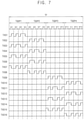
- FIG. 7 is a timing diagram for describing an example of driving a touch sensor using a touch driving code of FIG. 6 .
- FIG. 8 is a diagram illustrating another example of a touch driving code used for driving a touch sensor according to an example embodiment.
- FIG. 9 is a timing diagram for describing an example of driving a touch sensor using a touch driving code of FIG. 8 .
- FIG. 10 is a block diagram illustrating a display device according to an example embodiment.
- FIG. 11 is a diagram illustrating an example of a touch sensor and a touch controller included in the display device of FIG. 10 .
- FIG. 12 is an electronic device including a display device according to an example embodiment.
- FIG. 1 is a diagram illustrating a touch sensor according to an example embodiment
- FIG. 2 is a diagram for describing an example of parasitic capacitors of a touch sensor
- FIG. 3 is a diagram for describing an example of parasitic capacitors of a touch sensor in a case where adjacent touch driving channels are substantially simultaneously driven
- FIG. 4 is a diagram for describing an example of parasitic capacitors of a touch sensor according to an example embodiment.
- a touch sensor 100 may include a plurality of touch driving electrodes TX 1 through TX 8 , a plurality of touch driving lines TXL 1 through TXL 8 , a plurality of touch sensing electrodes RX 1 through RX 8 , and a plurality of touch sensing lines RXL 1 through RXL 8 .
- the touch sensor 100 may have a plurality of touch driving columns TDC 1 through TDC 5 , and each of the touch driving columns TDC 1 through TDC 5 includes the plurality of touch driving electrodes TX 1 through TX 8 .
- the touch driving electrodes TX 1 through TX 8 are respectively connected to corresponding touch driving lines TXL 1 through TXL 8 .
- each touch driving electrode TX 1 through TX 8 may be arranged in a (2N ⁇ 1)-th touch row and a 2N-th touch row, where N is an integer greater than 0. For example, as illustrated in FIG.
- the first touch driving electrode TX 1 may be arranged in first and second touch rows TR 1 and TR 2
- the second touch driving electrode TX 2 may be arranged in third and fourth touch rows TR 3 and TR 4
- the third touch driving electrode TX 3 may be arranged in fifth and sixth touch rows TR 5 and TR 6
- the fourth touch driving electrode TX 4 may be arranged in seventh and eighth touch rows TR 7 and TR 8
- the fifth touch driving electrode TX 5 may be arranged in ninth and tenth touch rows TR 9 and TR 10
- the sixth touch driving electrode TX 6 may be arranged in eleventh and twelfth touch rows TR 11 and TR 12
- the seventh touch driving electrode TX 7 may be arranged in thirteenth and fourteenth touch rows TR 13 and TR 14
- the eighth touch driving electrode TX 8 may be arranged in fifteenth and sixteenth touch rows TR 15 and TR 16 .
- the plurality of touch driving lines TXL 1 through TXL 8 may be respectively connected to the plurality of touch driving electrodes TX 1 through TX 8 , and may respectively transfer touch driving signals to the plurality of touch driving electrodes TX 1 through TX 8 .
- the touch driving lines (e.g., TXL 1 ) connected to the touch driving electrodes (e.g., TX 1 ) in the same touch rows (e.g., TR 1 and TR 2 ) may provide the same touch driving signal to the touch driving electrodes (e.g., TX 1 ). For example, as illustrated in FIG.
- the first touch driving lines TXL 1 extending in the first through fifth touch driving columns TDC 1 through TDC 5 may transfer the same first touch driving signal to the first touch driving electrodes TX 1 that are disposed in the first and second touch rows TR 1 and TR 2
- the second touch driving lines TXL 2 extending in the first through fifth touch driving columns TDC 1 through TDC 5 may transfer the same second touch driving signal to the second touch driving electrodes TX 2 that are disposed in the third and fourth touch rows TR 3 and TR 4
- the third touch driving lines TXL 3 extending in the first through fifth touch driving columns TDC 1 through TDC 5 may transfer the same third touch driving signal to the third touch driving electrodes TX 3 that are disposed in the fifth and sixth touch rows TR 5 and TR 6
- the fourth touch driving lines TXL 4 extending in the first through fifth touch driving columns TDC 1 through TDC 5 may transfer the same fourth touch driving signal to the fourth touch driving electrodes TX 4 that are disposed in the seventh and eighth touch rows TR 7 and TR 8
- the touch driving electrodes e.g., TX 1
- the touch driving electrodes that are located in the same touch rows (e.g., TR 1 and TR 2 ) and the different touch driving columns TDC 1 through TDC 5 may receive the same touch driving signal from the same touch driving channel of a touch controller (e.g., a touch controller 540 in FIG. 10 ), and may be substantially simultaneously driven based on the same touch driving signal.
- a touch controller e.g., a touch controller 540 in FIG. 10
- odd-numbered touch driving lines TXL 1 , TXL 3 , TXL 5 , and TXL 7 that are connected to odd-numbered touch driving electrodes TX 1 , TX 3 , TX 5 , and TX 7 for transferring the touch driving signals received from odd-numbered touch driving channels may be located at a first side (e.g., a right side) of the plurality of touch driving electrodes TX 1 through TX 8 , and even-numbered touch driving lines TXL 2 , TXL 4 , TXL 6 , and TXL 8 that are connected to even-numbered touch driving electrodes TX 2 , TX 4 , TX 6 , and TX 8 for transferring the touch driving signals received from even-numbered touch driving channels may be located at a second side (e.g., a left side) opposite to the first side of the plurality of touch driving electrodes TX 1 through TX 8 .
- a second side e.g., a left side
- the first through eighth touch driving electrodes TX 1 through TX 8 may be arranged in sequence in each touch driving column TDC 1 through TDC 5 , the first, third, fifth and seventh touch driving electrodes touch driving lines TXL 1 , TXL 3 , TXL 5 , and TXL 7 that are connected to the first, third, fifth, and seventh touch driving electrodes TX 1 , TX 3 , TX 5 , and TX 7 may be located at the right side of the first through eighth touch driving electrodes TX 1 through TX 8 , and the second, fourth, sixth, and eighth touch driving lines TXL 2 , TXL 4 , TXL 6 , and TXL 8 that are connected to the second, fourth, sixth, and eighth touch driving electrodes TX 2 , TX 4 , TX 6 , and TX 8 may be located at the left side of the first through eighth touch driving electrodes TX 1 through TX 8 .
- FIG. 1 illustrates an example of the touch sensor 100 that has the five touch driving columns TDC 1 through TDC 5 and includes the eight touch driving electrodes TX 1 through TX 8 and the eight touch driving lines TXL 1 through TX 8 in each touch driving column TDC 1 through TDC 5
- the number of touch driving columns, the number of the touch driving electrodes in each touch driving column, and the number of touch driving lines corresponding to the touch driving electrodes may not be limited to the example illustrated in FIG. 1 .
- the touch sensor 100 may have a plurality of touch sensing columns TSC 1 through TSC 4 that are alternately located with respect to the plurality of touch driving columns TDC 1 through TDC 5 .
- each touch sensing column some electrodes of the touch sensing electrodes RX 1 through RX 8 are connected alternately to two touch sensing lines of the touch sensing lines RXL 1 through RXL 8 .
- the first and eighth touch sensing electrodes RX 1 and RX 8 are arranged in the first touch sensing column TSC 1 and connected alternatively to the first and eighth touch sensing lines RXL 1 and RXL 8 .
- each touch sensing electrode RX 1 through RX 8 may be arranged in an (2N ⁇ 2)-th touch row and the (2N ⁇ 1)-th touch row. For example, as illustrated in FIG.
- first through fourth touch sensing electrodes RX 1 , RX 2 , RX 3 , and RX 4 may be located in the first touch row TR 1
- eighth through fifth touch sensing electrodes RX 8 , RX 7 , RX 6 , and RX 5 may be located in the second and third touch rows TR 2 and TR 3
- the first through fourth touch sensing electrodes RX 1 , RX 2 , RX 3 , and RX 4 may be located in the fourth and fifth touch rows TR 4 and TR 5
- the eighth through fifth touch sensing electrodes RX 8 , RX 7 , RX 6 , and RX 5 may be located in the sixth and seventh touch rows TR 6 and TR 7
- the first through fourth touch sensing electrodes RX 1 , RX 2 , RX 3 , and RX 4 may be located in the eighth and ninth touch rows TR 8 and TR 9
- two touch sensing lines may be located in each touch sensing column (e.g., TSC 1 ), odd-numbered touch sensing electrodes (e.g., RX 1 ) among the plurality of touch sensing electrodes (e.g., RX 1 and RX 8 ) in each touch sensing column (e.g., TSC 1 ) may be connected to one (e.g., RXL 1 ) of the two touch sensing lines (e.g., RXL 1 and RXL 8 ), and even-numbered touch sensing electrodes (e.g., RX 8 ) among the plurality of touch sensing electrodes (e.g., RX 1 and RX 8 ) in each touch sensing column (e.g., TSC 1 ) may be connected to the other (e.g., RXL 8 ) of the two touch sensing lines (e.g., RXL 1 and RXL 8 ).
- the odd-numbered touch sensing electrodes RX 1 in the first touch sensing column TSC 1 may be connected to the first touch sensing line RXL 1
- the odd-numbered touch sensing electrodes RX 2 in the second touch sensing column TSC 2 may be connected to the second touch sensing line RXL 2
- the odd-numbered touch sensing electrodes RX 3 in the third touch sensing column TSC 3 may be connected to the third touch sensing line RXL 3
- the odd-numbered touch sensing electrodes RX 4 in the fourth touch sensing column TSC 4 may be connected to the fourth touch sensing line RXL 4 .
- the even-numbered touch sensing electrodes RX 5 in the fourth touch sensing column TSC 4 may be connected to the fifth touch sensing line RXL 5
- the even-numbered touch sensing electrodes RX 6 in the third touch sensing column TSC 3 may be connected to the sixth touch sensing line RXL 6
- the even-numbered touch sensing electrodes RX 7 in the second touch sensing column TSC 2 may be connected to the seventh touch sensing line RXL 7
- the even-numbered touch sensing electrodes RX 8 in the first touch sensing column TSC 1 may be connected to the eighth touch sensing line RXL 8 .
- first through eighth touch sensing line RXL 1 through RXL 8 may be connected to first through eighth touch sensing channels of the touch controller (e.g., the touch controller 540 in FIG. 10 ), and may transfer first through eighth touch sensing signals induced at first through eighth touch sensing electrodes RX 1 through RX 8 to the first through eighth touch sensing channels, respectively.
- the touch controller e.g., the touch controller 540 in FIG. 10
- first through eighth touch sensing signals induced at first through eighth touch sensing electrodes RX 1 through RX 8 to the first through eighth touch sensing channels, respectively.
- each touch sensing column e.g., TSC 1
- the one (e.g., RXL 1 ) of the two touch sensing lines may be located at a first side (e.g., a right side) of the plurality of touch sensing electrodes (e.g., RX 1 and RX 8 ), and the other (e.g., RXL 8 ) of the two touch sensing lines (e.g., RXL 1 and RXL 8 ) may be located at a second side (e.g., a left side) opposite to the first side of the plurality of touch sensing electrodes (e.g., RX 1 and RX 8 ).
- FIG. 1 illustrates an example of the touch sensor 100 that has the four touch sensing columns TSC 1 through TSC 4 and includes two touch sensing electrodes (e.g., RX 1 and RX 8 ) and the two touch sensing lines (e.g., RXL 1 and RXL 8 ) in each touch sensing column (e.g., TSC 1 ), the number of touch sensing columns, the number of the touch sensing electrodes and the number of touch sensing lines in each touch sensing column may not be limited to the example of FIG. 1 . Further, although FIG.
- the touch sensor 100 may have a touch sensing column at the left edge, at the right edge, or at the left and right edges.
- the touch sensor 100 may be a one-layer (1-L) touch sensor where the plurality of touch driving electrodes TX 1 through TX 8 , the plurality of touch driving lines TXL 1 through TXL 8 , the plurality of touch sensing electrodes RX 1 through RX 8 , and the plurality of touch sensing lines RXL 1 through RXL 8 are formed in a single layer.
- a thickness of the touch sensor 100 may be reduced.
- each touch driving electrode TX 1 through TX 8 may be arranged in the (2N ⁇ 1)-th touch row and the 2N-th touch row
- each touch sensing electrode RX 1 through RX 8 may be arranged in the (2N ⁇ 2)-th touch row and the (2N ⁇ 1)-th touch row
- each touch driving electrode e.g., TX 1
- each touch driving electrode may be adjacent to two touch sensing electrodes (e.g., RX 1 and RX 8 ) at one side of the touch driving electrode (e.g., TX 1 ).
- each touch driving electrode e.g., the second touch driving electrode TX 2 in the second touch driving column TDC 2
- each touch driving electrode may be adjacent to four touch sensing electrodes (e.g., RX 1 , RX 2 , RX 7 , and RX 8 ).
- adjacent touch driving and sensing electrodes e.g., TX 1 and RX 8
- a resolution and an accuracy of the touch sensor 100 may be improved.
- the touch driving signals may be provided to the plurality of touch driving electrodes TX 1 through TX 8 through the plurality of touch driving lines TXL 1 through TXL 8 , the touch sensing signals may be induced at the plurality of touch sensing electrodes RX 1 through RX 8 based on the touch driving signals by capacitive coupling between the plurality of touch driving electrodes TX 1 through TX 8 and the plurality of touch sensing electrodes RX 1 through RX 8 , and the touch sensing signals may be output through the plurality of touch sensing lines RXL 1 through RXL 8 .
- the touch sensor 100 may detect a change of a mutual capacitance between a corresponding touch driving electrode and a corresponding touch sensing electrode caused by a touch input by a conductive object based on the touch sensing signals output through the plurality of touch sensing lines RXL 1 through RXL 8 and detect a touch row (e.g., touch rows TR 1 through TR 16 ) and a touch column (e.g., touch columns TC 1 through TC 8 ) corresponding to the touch input.
- a touch row e.g., touch rows TR 1 through TR 16
- a touch column e.g., touch columns TC 1 through TC 8
- a touch input in the first and second rows TR 1 and TR 2 and first through eighth touch columns TC 1 through TC 8 may be detected based on the touch sensing signals received from the first through eighth touch sensing electrodes RX 1 through RX 8 .
- the second touch driving electrodes TX 2 are driven, a touch input in the third and fourth touch rows TR 3 and TR 4 and the first through eighth touch columns TC 1 through TC 8 may be detected.
- the third touch driving electrodes TX 3 are driven, a touch input in the fifth and sixth touch rows TR 5 and TR 6 and the first through eighth touch columns TC 1 through TC 8 may be detected.
- a touch input in the seventh and eighth touch rows TR 7 and TR 8 and the first through eighth touch columns TC 1 through TC 8 may be detected.
- the fifth touch driving electrodes TX 5 are driven, a touch input in the ninth and tenth touch rows TR 9 and TR 10 and the first through eighth touch columns TC 1 through TC 8 may be detected.
- the sixth touch driving electrodes TX 6 are driven, a touch input in the eleventh and twelfth touch rows TR 11 and TR 12 and the first through eighth touch columns TC 1 through TC 8 may be detected.
- FIG. 1 illustrates an example where the touch sensor 100 may detect a touch input in the sixteen touch rows TR 1 through TR 16 and the eight touch columns TC 1 through TC 8 , the number of touch rows and the number of touch columns may not be limited to the example of FIG. 1 .
- a parasitic capacitance between adjacent lines and/or adjacent electrodes may increase power consumption and a noise in the lines and the electrodes.
- the touch sensor 100 may detect a touch input in the first touch row TR 1 and the first touch column TC 1 by detecting a capacitance change of a target capacitor CTARGET between the first touch driving electrode TX 1 in the first touch driving column TDC 1 and the first touch sensing electrode RX 1 in the first touch sensing column TSC 1 that is adjacent to the first touch driving column TDC 1 .
- the first touch driving electrode TX 1 and the first touch driving line TXL 1 may be driven or activated.
- a first parasitic capacitor PC 1 may be formed between the first touch driving line TXL 1 and the third touch driving line TXL 3 that is adjacent to the first touch driving line TXL 1 , and power for charging the first parasitic capacitor PC 1 may be additionally consumed in driving the first touch driving line TXL 1 .
- a second parasitic capacitor PC 2 may be formed between the first touch driving line TXL 1 and the eighth touch sensing line RXL 8 that is adjacent to the first touch driving line TXL 1
- a third parasitic capacitor PC 3 may be formed between the first touch driving line TXL 1 and the eighth touch sensing electrode RX 8 that is adjacent to the first touch driving line TXL 1
- a noise may occur in the touch driving signal that is applied to the first touch driving electrode TX 1 and/or in the touch sensing signals that is output through the touch sensing lines RXL 1 and RXL 8 .
- the parasitic capacitors may increase the power consumption and a noise in the touch driving signals and/or the touch sensing signals not only in a case where a single touch driving channel (or a touch driving channel connected to the first touch driving line TXL 1 ) is driven as illustrated in FIG. 2 , but also in a case where adjacent touch driving channels are substantially simultaneously driven as illustrated in FIG. 3 .
- FIG. 3 illustrates an example of the touch sensor 100 that drives adjacent first through fourth touch driving channels substantially simultaneously.
- FIG. 3 shows a portion of the touch sensor 100 where the sixteenth touch row TR 16 crosses the first touch sensing column TSC 1 , the second touch driving column TDC 2 , and the second touch sensing column TSC 2 .
- first parasitic capacitors PC 11 through PC 14 may be formed between the driven touch driving lines (e.g., TXL 4 and TXL 3 ) and non-driven touch driving lines (e.g., TXL 5 through TXL 8 ) consuming additional power to charge the parasitic capacitors PC 11 through PC 14 .
- second parasitic capacitors PC 21 through PC 24 may be formed between the driven touch driving lines TXL 1 through TXL 4 and adjacent touch sensing lines RXL 1 and RXL 7 may cause a noise in the touch driving signal and/or the touch sensing signals.
- the touch sensor 100 in each touch driving column TDC 1 through TDC 5 , may drive two or more odd-numbered touch driving electrodes TX 1 , TX 3 , TX 5 and TX 7 among the plurality of touch driving electrodes TX 1 through TX 8 substantially simultaneously during a first touch group driving period, and drive two or more even-numbered touch driving electrodes TX 2 , TX 4 , TX 6 and TX 8 among the plurality of touch driving electrodes TX 1 through TX 8 substantially simultaneously during a second touch group driving period that is different from the first touch group driving period.
- the touch driving signals TX 5 may be substantially simultaneously applied to the odd-numbered touch driving electrodes TX 1 , TX 3 , TX 5 , and TX 7 through the odd-numbered touch driving lines TXL 1 , TXL 3 , TXL 5 , and TXL 7 during the first touch group driving period, and the touch driving signals TX 5 may be substantially simultaneously applied to the even-numbered touch driving electrodes TX 2 , TX 4 , TX 6 , and TX 8 through the even-numbered touch driving lines TXL 2 , TXL 4 , TXL 6 , and TXL 8 during the second touch group driving period.
- the first through eighth touch driving electrodes TX 1 through TX 8 may be arranged in sequence in each touch driving column TDC 1 through TDC 5 , the first, third, fifth, and seventh touch driving electrodes TX 1 , TX 3 , TX 5 , and TX 7 may be substantially simultaneously driven during the first touch group driving period, and the second, fourth, sixth, and eighth touch driving electrodes TX 2 , TX 4 , TX 6 , and TX 8 may be substantially simultaneously driven during the second touch group driving period.
- the touch sensor 100 may reduce the power consumption and a noise in the touch driving signals and/or the touch sensing signals by driving the odd-numbered touch driving electrodes TX 1 , TX 3 , TX, 5 and TX 7 substantially simultaneously, and driving the even-numbered touch driving electrodes TX 2 , TX 4 , TX 6 , and TX 8 substantially simultaneously during different touch group driving periods.
- FIG. 4 illustrates a portion of the touch sensor 100 where the sixteenth touch row TR 16 crosses the first touch sensing column TSC 1 , the second touch driving column TDC 2 , and the second touch sensing column TSC 2 . Referring to FIG.
- the odd-numbered touch driving electrodes TX 1 , TX 3 , TX 5 , and TX 7 and the odd-numbered touch driving lines TXL 1 , TXL 3 , TXL 5 , and TXL 7 may be substantially simultaneously driven, and the driven touch driving lines TXL 1 , TXL 3 , TXL 5 , and TXL 7 may be spaced apart from the non-driven driven touch driving lines TXL 2 , TXL 4 , TXL 6 , and TXL 8 .
- the first parasitic capacitors PC 11 through PC 14 illustrated in FIG. 3 may not be formed. Accordingly, the touch sensor 100 may prevent or reduce the additional power consumption for charging the parasitic capacitors PC 11 through PC 14 .
- FIG. 3 shows the second parasitic capacitors PC 21 and PC 23 formed between the first and third touch driving lines TXL 1 and TXL 3 and the seventh touch sensing line RXL 7 and the second parasitic capacitors PC 22 and PC 24 formed between the second and fourth touch driving lines TXL 2 and TXL 4 and the first touch sensing line RXL 1
- the example of FIG. 4 shows the second parasitic capacitors PC 21 , PC 23 , PC 25 , and PC 27 formed between the first, third, fifth, and seventh touch driving electrodes touch driving lines TXL 1 , TXL 3 , TXL 5 , and TXL 7 and the seventh touch sensing line RXL 7 .
- a capacitance value of the second capacitor PC 21 between the first touch driving line TXL 1 and the seventh touch sensing line RXL 7 is 1, the second capacitor PC 23 between the third touch driving line TXL 3 and the seventh touch sensing line RXL 7 may have a capacitance value of about 0.5, the second capacitor PC 25 between the fifth touch driving line TXL 5 and the seventh touch sensing line RXL 7 may have a capacitance value of about 0.25, and the second capacitor PC 27 between the seventh touch driving line TXL 7 and the seventh touch sensing line RXL 7 may have a capacitance value of about 0.125. Further, the sign of the capacitance values may be positive or negative according to each touch driving signal has a rising edge or a falling edge.
- the touch sensor 100 shown in the example of FIG. 3 where the second capacitor PC 21 between the first touch driving line TXL 1 and the seventh touch sensing line RXL 7 has a capacitance value of about 1, the second capacitor PC 22 between the third touch driving line TXL 3 and the first touch sensing line RXL 1 has a capacitance value of about 1, the second capacitor PC 23 between the third touch driving line TXL 3 and the seventh touch sensing line RXL 7 has a capacitance value of about 0.5, and the second capacitor PC 24 between the fourth touch driving line TXL 4 and the first touch sensing line RXL 1 has a capacitance value of about 0.5, the touch sensor 100 shown in the example of FIG.
- the touch sensor 100 may reduce the capacitance of the second parasitic capacitors PC 21 , PC 23 , PC 25 and PC 27 . Accordingly, the touch sensor 100 may reduce the noise caused by the second parasitic capacitors PC 21 , PC 23 , PC 25 and PC 27 in the touch driving signal and/or the touch sensing signals.
- the touch sensor 100 may drive the odd-numbered touch driving electrodes TX 1 , TX 3 , TX 5 , and TX 7 substantially simultaneously, and the even-numbered touch driving electrodes TX 2 , TX 4 , TX 6 , and TX 8 substantially simultaneously in different touch group driving periods. Accordingly, the touch sensor 100 may reduce an undesired parasitic capacitance between the touch driving lines TXL 1 through TXL 8 and the touch sensing lines RXL 1 through RXL 8 and the touch driving electrodes TX 1 through TX 8 and the touch sensing electrodes RX 1 through RX 8 , thereby reducing power consumption and a noise in the touch driving signals and/or the touch sensing signals.
- FIG. 5 is a flowchart illustrating a method of driving a touch sensor according to an example embodiment
- FIG. 6 is a diagram illustrating an example of a touch driving code used for driving a touch sensor according to an example embodiment
- FIG. 7 is a timing diagram for describing an example of driving a touch sensor using a touch driving code of FIG. 6
- FIG. 8 is a diagram illustrating another example of a touch driving code used for driving a touch sensor according to an example embodiment
- FIG. 9 is a timing diagram for describing an example of driving a touch sensor using a touch driving code of FIG. 8 .
- the touch sensor 100 may drive two or more odd-numbered touch driving electrodes (e.g., TX 1 , TX 3 , TX 5 , and TX 7 ) among a plurality of touch driving electrodes TX 1 through TX 8 in each touch driving column TDC 1 through TDC 5 substantially simultaneously during a first touch group driving period (S 210 ), and two or more even-numbered touch driving electrodes TX 2 , TX 4 , TX 6 , and TX 8 among the plurality of touch driving electrodes TX 1 through TX 8 in each touch driving column TDC 1 through TDC 5 substantially simultaneously during a second touch group driving period that is different from the first touch group driving period (S 230 ).
- odd-numbered touch driving electrodes e.g., TX 1 , TX 3 , TX 5 , and TX 7
- TX 1 through TX 8 in each touch driving column TDC 1 through TDC 5 substantially simultaneously during a first touch group driving period (S 210 )
- touch driving signals may be substantially simultaneously applied to the odd-numbered touch driving electrodes TX 1 , TX 3 , TX 5 , and TX 7 through odd-numbered touch driving lines TXL 1 , TXL 3 , TXL 5 , and TXL 7 located at a first side (e.g., a right side) of the plurality of touch driving electrodes TX 1 through TX 8 in each touch driving column TDC 1 through TDC 5 .
- the touch driving signals may be substantially simultaneously applied to the even-numbered touch driving electrodes TX 2 , TX 4 , TX 6 , and TX 8 through even-numbered touch driving lines TXL 2 , TXL 4 , TXL 6 , and TXL 8 located at a second side (e.g., a left side) opposite to the first side of the plurality of touch driving electrodes TX 1 through TX 8 in each touch driving column TDC 1 through TDC 5 .
- a second side e.g., a left side
- simultaneous driving of the odd-numbered touch driving electrodes TX 1 , TX 3 , TX 5 , and TX 7 (S 210 ) and this simultaneous driving of the even-numbered touch driving electrodes TX 2 , TX 4 , TX 6 , and TX 8 (S 230 ) may be repeated until all of the touch driving electrodes TX 1 through TX 8 are driven (S 250 ).
- FIG. 6 shows an example of a touch driving code 300 that is used to drive the touch sensor 100 as illustrated in FIG. 7 .
- FIG. 7 illustrates an example where the touch sensor 100 includes sixteen touch driving lines in each touch driving column TDC 1 through TDC 5 , and first through sixteenth touch driving signals TXS 1 through TXS 16 are applied to the sixteen touch driving lines, respectively.
- each touch frame TF may include first through fourth touch group driving periods TGDP 1 through TGDP 4 , and, in each touch group driving period, four touch driving signals may be applied to four touch driving lines, respectively.
- the touch driving signals TXS 1 , TXS 3 , TXS 5 , and TXS 7 are applied to the touch driving lines TXL 1 , TXL 3 , TXL 5 , and TXL 7 , respectively.
- the first touch group driving period TGDP 1 may include first through fourth touch group driving sub-periods SP 1 through SP 4
- the second touch group driving period TGDP 2 may include fifth through eighth touch group driving sub-periods SP 5 through SP 8
- the third touch group driving period TGDP 3 may include ninth through twelfth touch group driving sub-periods SP 9 through SP 12
- the fourth touch group driving period TGDP 4 may include thirteenth through sixteenth touch group driving sub-periods SP 13 through SP 16 .
- a touch driving signal having a rising edge is represented as a value of 1
- a touch driving signal having a falling edge is represented as a value of ⁇ 1.
- each touch group driving sub-period (e.g., SP 1 ) of the touch driving code 300 three touch driving signals (e.g., TXS 1 , TXS 3 and TXS 5 ) may have a rising edge, and the remaining one of the touch driving signal (e.g., TXS 7 ) may have a falling edge. Further, in respective touch group driving sub-periods SP 1 , SP 2 , SP 3 , and SP 4 , the touch driving signals TXS 1 , TXS 3 , TXS 5 , and TXS 7 may alternately have a falling edge.
- the first, third, and fifth touch driving signals TXS 1 , TXS 3 , and TXS 5 having a rising edge may be applied to the first, third, and fifth touch driving electrodes TX 1 , TX 3 , and TX 5
- the seventh touch driving signal TXS 7 having a falling edge may be applied to the seventh touch driving electrode TX 7 .
- the first, third, and seventh touch driving signals TXS 1 , TXS 3 , and TXS 7 having a rising edge may be applied to the first, third, and seventh touch driving electrodes TX 1 , TX 3 , and TX 7
- the fifth touch driving signal TXS 5 having a falling edge may be applied to the fifth touch driving electrode TX 5 .
- the first, fifth, and seventh touch driving signals TXS 1 , TXS 5 , and TXS 7 having a rising edge may be applied to the first, fifth, and seventh touch driving electrodes TX 1 , TX 5 , and TX 7
- the third touch driving signal TXS 3 having a falling edge may be applied to the third touch driving electrode TX 3 .
- the third, fifth, and seventh touch driving signals TXS 3 , TXS 5 , and TXS 7 having a rising edge may be applied to the third, fifth, and seventh touch driving electrodes TX 3 , TX 5 , and TX 7
- the first touch driving signal TXS 1 having a falling edge may be applied to the first touch driving electrode TX 1 .
- the touch sensor 100 may drive the odd-numbered touch driving electrodes TX 1 , TX 3 , TX 5 , and TX 7 , or the first, third, fifth, and seventh touch driving electrodes TX 1 , TX 3 , TX 5 , and TX 7 substantially simultaneously in the first touch group driving period TGDP 1 .
- the second, fourth, and sixth touch driving signals TXS 2 , TXS 4 , and TXS 6 having a rising edge may be applied to second, fourth, and sixth touch driving electrodes TX 2 , TX 4 , and TX 6
- the eighth touch driving signal TXS 8 having a falling edge may be applied to the eighth touch driving electrode TX 8 .
- the second, fourth, and eighth touch driving signals TXS 2 , TXS 4 , and TXS 8 having a rising edge may be applied to the second, fourth, and eighth touch driving electrodes TX 2 , TX 4 , and TX 8
- the sixth touch driving signal TXS 6 having a falling edge may be applied to the sixth touch driving electrode TX 6 .
- the second, sixth, and eighth touch driving signals TXS 2 , TXS 6 , and TXS 8 having a rising edge may be applied to the second, sixth, and eighth touch driving electrodes TX 2 , TX 6 , and TX 8
- the fourth touch driving signal TXS 4 having a falling edge may be applied to the fourth touch driving electrode TX 4 .
- the fourth, sixth, and eighth touch driving signals TXS 4 , TXS 6 , and TXS 8 having a rising edge may be applied to the fourth, sixth, and eighth touch driving electrodes TX 4 , TX 6 , and TX 8 , and the second touch driving signal TXS 2 having a falling edge to the second touch driving electrode TX 2 .
- the touch sensor 100 may drive, the even-numbered touch driving electrodes TX 2 , TX 4 , TX 6 , and TX 8 , or the second, fourth, sixth, and eighth touch driving electrodes TX 2 , TX 4 , TX 6 , and TX 8 substantially simultaneously in the second touch group driving period TGDP 2 .
- the ninth, eleventh, thirteenth, and fifteenth touch driving signals TXS 9 , TXS 11 , TXS 13 , and TXS 15 may be applied to the next odd-numbered touch driving electrodes, or ninth, eleventh, thirteenth, and fifteenth touch driving electrodes, and the touch sensor 100 may drive the ninth, eleventh, thirteenth and fifteenth touch driving electrodes substantially simultaneously.
- the tenth, twelfth, fourteenth, and sixteenth touch driving signals TXS 10 , TXS 12 , TXS 14 , and TXS 16 may be applied to the next even-numbered touch driving electrodes, or tenth, twelfth, fourteenth, and sixteenth touch driving electrodes, and the touch sensor 100 may drive the tenth, twelfth, fourteenth and sixteenth touch driving electrodes substantially simultaneously.
- FIG. 8 shows another example of a touch driving code 400 that is used to drive the touch sensor 100 as illustrated in FIG. 9 .
- a touch driving code 400 that is used to drive the touch sensor 100 as illustrated in FIG. 9 .
- three touch driving signals e.g., TXS 1 , TXS 3 , and TXS 5
- TXS 7 may have a rising edge represented as value of 1.
- the touch driving signals TXS 1 , TXS 3 , TXS 5 , and TXS 7 may alternately have a rising edge.
- the touch sensor 100 may drive the first, third, fifth, and seventh touch driving electrodes TX 1 , TX 3 , TX 5 , and TX 7 substantially simultaneously in the first touch group driving period TGDP 1 , and may drive the second, fourth, sixth, and eighth touch driving electrodes TX 2 , TX 4 , TX 6 , and TX 8 substantially simultaneously in the second touch group driving period TGDP 2 , may drive the ninth, eleventh, thirteenth, and fifteenth touch driving electrodes substantially simultaneously in the third touch group driving period TGDP 3 , and may drive the tenth, twelfth, fourteenth, and sixteenth touch driving electrodes substantially simultaneously in the fourth touch group driving period TGDP 4 .
- FIGS. 6 and 8 illustrate the examples of the touch driving codes 300 and 400 , and the touch driving code that may be used for driving the touch sensor 100 may not be limited to the examples of FIGS. 6 and 8 .
- the touch sensor 100 may drive the odd-numbered touch driving electrodes TX 1 , TX 3 , TX 5 , and TX 7 substantially simultaneously, and the even-numbered touch driving electrodes TX 2 , TX 4 , TX 6 , and TX 8 substantially simultaneously in different touch group driving periods. Accordingly, the touch sensor 100 may reduce an undesired parasitic capacitance between the touch driving lines TXL 1 through TXL 8 and the touch sensing lines RXL 1 through RXL 8 and the touch driving electrodes TX 1 through TX 8 and the touch sensing electrodes RX 1 through RX 8 , thereby reducing power consumption and a noise in the touch driving signals and/or the touch sensing signals.
- FIG. 10 is a block diagram illustrating a display device according to an example embodiment
- FIG. 11 is a diagram illustrating an example of a touch sensor and a touch controller included in the display device of FIG. 10 .
- a display device 500 may include a display panel 510 including a plurality of pixels PX, a touch sensor 520 on the plurality of pixels PX, a display driver 530 for driving the plurality of pixels PX, and a touch controller 540 for controlling the touch sensor 520 .
- the display driver 530 may drive the display panel 510 to display an image.
- the display panel 510 may further include a plurality of data lines and a plurality of scan lines, and each of the pixels PX is coupled to respective ones of the data lines and the scan lines.
- the display panel 510 may be an organic light emitting diode (OLED) display panel where each pixel PX includes an OLED.
- the display panel 510 may be a liquid crystal display (LCD) panel, a light emitting diode (LED) display panel, a field emission display (FED) panel, or any other suitable display panel.
- the display driver 530 may drive the display panel 510 based on input image data IDAT and a control signal CTRL received from an external processor (e.g., a graphic processing unit (GPU), an application processor (AP), or a graphic card).
- the input image data IDAT may be RGB image data including red image data, green image data, and blue image data.
- the control signal CTRL may include, but is not limited to, a vertical synchronization signal, a horizontal synchronization signal, an input data enable signal, a master clock signal, etc.
- the display driver 530 may generate display panel driving signals DPS based on the input image data IDAT and the control signal CTRL and drive the display panel 510 by providing the display panel driving signals DPS to the display panel 510 .
- the display panel driving signals DPS may include scan signals and data signals.
- the display driver 530 may include a scan driver for providing the scan signals to the display panel 510 , a data driver for providing the data signals to the display panel 510 , and a timing controller for controlling the scan driver and the data driver.
- the touch sensor 520 may be a capacitive touch sensor that detects a change in capacitance caused by a touch input by a conductive object (e.g., a finger, a stylus pen, etc.).
- the touch sensor 520 may correspond to the touch sensor 100 illustrated in FIG. 1 that may have the plurality of touch driving columns TDC 1 through TDC 5 and the plurality of touch sensing columns TSC 1 through TSC 4 , and may include the plurality of touch driving electrodes TX 1 through TX 8 in each touch driving column TDC 1 through TDC 5 , and the plurality of touch sensing electrodes (e.g., RX 1 and RX 8 ) in each touch sensing column (e.g., TSC 1 ).
- the touch sensor 520 may be a one-layer (1-L) touch sensor where the plurality of touch driving electrodes TX 1 through TX 8 and the plurality of touch sensing electrodes RX 1 through RX 8 are formed in a single layer. Further, as illustrated in FIG. 1 , each touch driving electrode TX 1 through TX 8 and each touch sensing electrode RX 1 through RX 8 may have a rectangular shape, but the shape of the touch driving electrodes and touch sensing electrodes is not limited to the rectangular shape. According to an example embodiment, the touch sensor 520 may be an add-on type touch sensor that is attached on the display panel 510 , or an embedded type touch sensor formed within or integrated with the display panel 510 . For example, the touch sensor 520 may be, but is not limited to, an on-cell type embedded touch sensor, or an in-cell type embedded touch sensor.
- the touch controller 540 may detect presence and/or a location of a touch input by the conductive object by driving the touch sensor 520 and sensing a change caused by the touch input. For example, the touch controller 540 may provide touch driving signals TX 5 to the plurality of touch driving electrodes TX 1 through TX 8 through the plurality of touch driving lines TXL 1 through TXL 8 , respectively. Touch sensing signals RX 5 may be induced at one or more of the plurality of touch sensing electrodes RX 1 through RX 8 based on the touch driving signals by capacitive coupling between the plurality of touch driving electrodes TX 1 through TX 8 and the plurality of touch sensing electrodes RX 1 through RX 8 .
- the touch controller 540 may receive the touch sensing signals RX 5 through the plurality of touch sensing lines RXL 1 through RXL 8 . Further, the touch controller 540 may detect a change of a mutual capacitance between a corresponding touch driving electrode TX 1 through TX 8 and a corresponding touch sensing electrode RX 1 through RX 8 caused by the touch input by the conductive object based on the touch sensing signals RX 5 , thereby detecting the presence and/or location of the touch input in a corresponding one of the touch rows TR 1 through TR 16 and a corresponding one of the touch columns TC 1 through TC 8 .
- FIG. 11 illustrates an example of the touch controller 540 that may include a touch driving circuit 550 for providing the touch driving signals TX 5 to the touch sensor 520 , and a touch sensing circuit 560 for receiving the touch sensing signals TX 5 from the touch sensor 520 .
- the touch driving circuit 550 may include first through eighth touch driving channels for providing the touch driving signals TX 5 to the first through eighth touch driving electrodes TX 1 through TX 8 through the first through eighth touch driving lines TXL 1 through TXL 8 , respectively. Further, the touch driving circuit 550 may substantially simultaneously drive two or more odd-numbered touch driving electrodes TX 1 , TX 3 , TX 5 , and TX 7 during a first touch group driving period, and may substantially simultaneously drive two or more even-numbered touch driving electrodes TX 2 , TX 4 , TX 6 , and TX 8 during a second touch group driving period that is different from the first touch group driving period.
- odd-numbered touch driving channels, or the first, third, fifth, and seventh touch driving channels of the touch driving circuit 550 may substantially simultaneously apply the touch driving signals TX 5 to the first, third, fifth, and seventh touch driving electrodes TX 1 , TX 3 , TX 5 , and TX 7 through the first, third, fifth, and seventh touch driving lines TXL 1 , TXL 3 , TXL 5 , and TXL 7 during the first touch group driving period, and even-numbered touch driving channels, or the second, fourth, sixth, and eighth touch driving channels of the touch driving circuit 550 may substantially simultaneously apply the touch driving signals TX 5 to the second, fourth, sixth, and eighth touch driving electrodes TX 2 , TX 4 , TX 6 , and TX 8 through the second, fourth, sixth, and eighth touch driving lines TXL 2 , TXL 4 , TXL 6 and TXL 8 .
- the touch sensor 520 may reduce an undesired parasitic capacitance between the touch driving lines TXL 1 through TXL 8 and the touch sensing lines RXL 1 through RXL 8 and the touch driving electrodes TX 1 through TX 8 and the touch sensing electrodes RX 1 through RX 8 , thereby reducing power consumption and a noise of the touch sensor 520 in the touch driving signals and/or the touch sensing signals.
- the touch sensing circuit 560 may include the first through eighth touch sensing channels 570 for receiving the touch sensing signals RX 5 from the first through eighth touch sensing electrodes RX 1 through RX 8 through the first through eighth touch sensing lines RXL 1 through RXL 8 , respectively.
- each touch sensing channel 570 may include, but is not limited to, an amplifier AMP, a capacitor CAP, a switch SW, and an analog-to-digital converter ADC.
- the touch sensing signal RX 5 received by each touch sensing channel 570 may be converted from an analog signal into a digital signal.
- the touch controller 540 may generate touch data TD representing a detected touch input based on the digital signals that are output from the first through eighth touch sensing channels 570 , and may provide the touch data TD to the timing controller and/or the external processor.
- the touch sensor 520 of the display device 500 may drive the odd-numbered touch driving electrodes TX 1 , TX 3 , TX 5 , and TX 7 substantially simultaneously, and the even-numbered touch driving electrodes TX 2 , TX 4 , TX 6 , and TX 8 substantially simultaneously in different touch group driving periods. Accordingly, the touch sensor 520 may reduce the undesired parasitic capacitance between the touch driving lines TXL 1 through TXL 8 and the touch sensing lines RXL 1 through RXL 8 and the touch driving electrodes TX 1 through TX 8 and the touch sensing electrodes RX 1 through RX 8 , thereby reducing power consumption and a noise in the touch driving signals and/or the touch sensing signals.
- FIG. 12 is an electronic device including a display device according to an example embodiment.
- an electronic device 1100 may include a processor 1110 , a memory device 1120 , a storage device 1130 , an input/output (I/O) device 1140 , a power supply 1150 , and a display device 1160 .
- the electronic device 1100 may further include a plurality of ports for communicating with various peripheral components and/or devices such as a video card, a sound card, a memory card, a universal serial bus (USB) device, other electric devices, etc.
- peripheral components and/or devices such as a video card, a sound card, a memory card, a universal serial bus (USB) device, other electric devices, etc.
- the processor 1110 may perform various computing functions or tasks.
- the processor 1110 may be an application processor (AP), a microprocessor, a central processing unit (CPU), etc.
- the processor 1110 may be coupled to other components via an address bus, a control bus, a data bus, etc. Further, the processor 1110 may be further coupled to an extended bus such as a peripheral component interconnection (PCI) bus.
- PCI peripheral component interconnection
- the memory device 1120 may store data for operating the electronic device 1100 .
- the memory device 1120 may include at least one non-volatile memory device such as an erasable programmable read-only memory (EPROM) device, an electrically erasable programmable read-only memory (EEPROM) device, a flash memory device, a phase change random access memory (PRAM) device, a resistance random access memory (RRAM) device, a nano floating gate memory (NFGM) device, a polymer random access memory (PoRAM) device, a magnetic random access memory (MRAM) device, a ferroelectric random access memory (FRAM) device, etc., and/or at least one volatile memory device such as a dynamic random access memory (DRAM) device, a static random access memory (SRAM) device, a mobile dynamic random access memory (mobile DRAM) device, etc.
- DRAM dynamic random access memory
- SRAM static random access memory
- mobile DRAM mobile dynamic random access memory
- the storage device 1130 may be a solid state drive (SSD) device, a hard disk drive (HDD) device, a CD-ROM device, etc.
- the I/O device 1140 may include an input device such as a keyboard, a keypad, a mouse, a touch screen, etc., and an output device such as a printer, a speaker, etc.
- the power supply 1150 may supply power for operating the electronic device 1100 .
- the display device 1160 may be coupled to other components through buses or other communication links.
- the display device 1160 may include a touch sensor.
- the touch sensor may drive odd-numbered touch driving electrodes substantially simultaneously, and even-numbered touch driving electrodes substantially simultaneously in different touch group driving periods. Accordingly, the touch sensor may reduce an undesired parasitic capacitance between lines and electrodes of the touch sensor, thereby reducing power consumption and a noise in the touch sensor.
- the present inventive concepts may be applied any electronic device 1100 including the display device 1160 .
- the present inventive concepts may be applied to a mobile phone, a smart phone, a tablet computer, a television (TV), a digital TV, a three-dimensional (3D) TV, a wearable electronic device, a personal computer (PC), a home appliance, a laptop computer, a personal digital assistant (PDA), a portable multimedia player (PMP), a digital camera, a music player, a portable game console, a navigation device, etc.
Landscapes
- Engineering & Computer Science (AREA)
- Theoretical Computer Science (AREA)
- General Engineering & Computer Science (AREA)
- Physics & Mathematics (AREA)
- General Physics & Mathematics (AREA)
- Human Computer Interaction (AREA)
- Quality & Reliability (AREA)
- Computer Networks & Wireless Communication (AREA)
- Control Of Indicators Other Than Cathode Ray Tubes (AREA)
Abstract
Description
Claims (20)
Applications Claiming Priority (2)
| Application Number | Priority Date | Filing Date | Title |
|---|---|---|---|
| KR1020190166361A KR20210076232A (en) | 2019-12-13 | 2019-12-13 | Touch sensor, display device, and method of driving a touch sensor |
| KR10-2019-0166361 | 2019-12-13 |
Publications (2)
| Publication Number | Publication Date |
|---|---|
| US20210181917A1 US20210181917A1 (en) | 2021-06-17 |
| US11269448B2 true US11269448B2 (en) | 2022-03-08 |
Family
ID=76317977
Family Applications (1)
| Application Number | Title | Priority Date | Filing Date |
|---|---|---|---|
| US16/987,323 Expired - Fee Related US11269448B2 (en) | 2019-12-13 | 2020-08-06 | Touch sensor, display device, and method of driving a touch sensor |
Country Status (3)
| Country | Link |
|---|---|
| US (1) | US11269448B2 (en) |
| KR (1) | KR20210076232A (en) |
| CN (1) | CN112987963A (en) |
Families Citing this family (1)
| Publication number | Priority date | Publication date | Assignee | Title |
|---|---|---|---|---|
| JP7438854B2 (en) * | 2020-06-05 | 2024-02-27 | シャープ株式会社 | touch panel input device |
Citations (39)
| Publication number | Priority date | Publication date | Assignee | Title |
|---|---|---|---|---|
| US20100144391A1 (en) * | 2008-12-05 | 2010-06-10 | Shih Chang Chang | Integrated touch panel for a TFT display |
| US20100149108A1 (en) * | 2008-12-11 | 2010-06-17 | Steve Porter Hotelling | Single layer touch panel with segmented drive and sense electrodes |
| US20130181943A1 (en) * | 2012-01-12 | 2013-07-18 | Synaptics Incorporated | Single layer capacitive imaging sensors |
| US20130307793A1 (en) * | 2012-05-16 | 2013-11-21 | Dongbu Hitek Co., Ltd. | Touch Screen Panel |
| US20140111707A1 (en) * | 2012-05-16 | 2014-04-24 | Joon SONG | Touch Screen Panel |
| US20140327644A1 (en) * | 2013-05-06 | 2014-11-06 | Rishi Mohindra | Papr optimized ofdm touch engine with tone spaced windowed demodulation |
| US20140333847A1 (en) * | 2013-05-09 | 2014-11-13 | Hannstar Display Corporation | Touch panel and touch display |
| US20140368750A1 (en) * | 2013-06-18 | 2014-12-18 | Novatek Microelectronics Corp. | Single-layer mutual capacitive touch screen |
| US20150077387A1 (en) * | 2013-09-13 | 2015-03-19 | Lg Display Co., Ltd. | Touch integrated circuit and touch screen display device including the same |
| US20150179122A1 (en) * | 2013-12-20 | 2015-06-25 | Sharp Kabushiki Kaisha | Discriminative capacitive touch panel |
| US20150185938A1 (en) * | 2013-12-26 | 2015-07-02 | Lg Display Co., Ltd. | Touch sensor integrated type display device |
| US20150205428A1 (en) * | 2013-03-29 | 2015-07-23 | Boe Technology Group Co., Ltd. | Touch screen, driving method thereof and display device |
| US20150370380A1 (en) * | 2012-07-23 | 2015-12-24 | Samsung Display Co., Ltd. | Touch screen panel and touch sensing apparatus having the same |
| US20160026290A1 (en) * | 2014-02-24 | 2016-01-28 | Boe Technology Group Co., Ltd. | In-cell touch panel and display device |
| US20160202829A1 (en) * | 2015-01-13 | 2016-07-14 | Samsung Display Co., Ltd. | Method for driving touch screen panel and touch screen panel employing the method |
| US20160253013A1 (en) * | 2014-07-08 | 2016-09-01 | Boe Technology Group Co., Ltd. | Touch three-dimensional grating and display device |
| US20160282981A1 (en) * | 2014-07-10 | 2016-09-29 | Boe Technology Group Co., Ltd. | Built-in touch display device and method for driving the same |
| US20160282995A1 (en) * | 2014-10-17 | 2016-09-29 | Raydium Semiconductor Corporation | In-cell mutual-capacitive touch panel |
| US9535523B2 (en) * | 2012-12-11 | 2017-01-03 | Lg Display Co., Ltd. | Touch sensor integrated type display device |
| US20170046003A1 (en) * | 2015-08-10 | 2017-02-16 | Shanghai Tianma Micro-electronics Co., Ltd. | Touch display substrate, electronic device and driving method |
| US20170115802A1 (en) * | 2015-10-22 | 2017-04-27 | Xiamen Tianma Micro-Electronics Co., Ltd. | Array substrate, touch display device and method for driving the same |
| US20170147127A1 (en) * | 2015-11-24 | 2017-05-25 | Xiamen Tianma Micro-Electronics Co., Ltd. | Array substrate, touch display device and driving method thereof |
| US20170168635A1 (en) * | 2015-12-14 | 2017-06-15 | Xiamen Tianma Micro-Electronics Co., Ltd. | Touch control device and touch display device |
| US20170177158A1 (en) * | 2016-10-31 | 2017-06-22 | Xiamen Tianma Micro-Electronics Co., Ltd. | Touch control display panel and touch control display device |
| US20170285837A1 (en) * | 2016-03-29 | 2017-10-05 | Shanghai Tianma Micro-electronics Co., Ltd. | Folding display device |
| US20170285823A1 (en) * | 2016-12-21 | 2017-10-05 | Xiamen Tianma Micro-Electronics Co., Ltd. | Array substrate, touch display panel, and touch display device |
| US20170336910A1 (en) * | 2016-05-20 | 2017-11-23 | Lg Display Co., Ltd. | Sensor screen perceiving touch and fingerprint |
| KR20170134836A (en) | 2016-05-26 | 2017-12-07 | 삼성디스플레이 주식회사 | Touch sensor |
| KR20170136072A (en) | 2016-05-30 | 2017-12-11 | 삼성디스플레이 주식회사 | Touch screen |
| US20180046276A1 (en) * | 2016-08-11 | 2018-02-15 | Focaltech Systems Co., Ltd. | Electronic apparatus and single-layer multi-point mutual capacitive touch screen thereof |
| US20180107379A1 (en) * | 2016-01-08 | 2018-04-19 | Boe Technology Group Co., Ltd. | Touch panel, touch control display device and method of driving the same |
| US20180113346A1 (en) * | 2016-10-24 | 2018-04-26 | Lg Display Co., Ltd. | Fingerprint sensor integrated type touch screen panel |
| KR20190010762A (en) | 2017-07-20 | 2019-01-31 | 삼성디스플레이 주식회사 | Touch sensor and display device having the same |
| US20190179475A1 (en) * | 2017-12-12 | 2019-06-13 | Lg Display Co., Ltd. | Display Apparatus |
| US20190204949A1 (en) * | 2018-01-03 | 2019-07-04 | Boe Technology Group Co., Ltd. | Touch Substrate and Display Device |
| US20190235678A1 (en) * | 2018-01-31 | 2019-08-01 | Samsung Display Co., Ltd. | Display device |
| US20200210025A1 (en) * | 2018-12-28 | 2020-07-02 | Lg Display Co., Ltd. | Touch display device, touch panel, touch sensing circuit, and touch sensing method |
| US20200241703A1 (en) * | 2017-09-25 | 2020-07-30 | Huawei Technologies Co., Ltd. | Array Substrate and Display Panel |
| US20200272329A1 (en) * | 2019-02-22 | 2020-08-27 | Novatek Microelectronics Corp. | Method for proximity sensing |
Family Cites Families (4)
| Publication number | Priority date | Publication date | Assignee | Title |
|---|---|---|---|---|
| CN203224861U (en) * | 2013-04-24 | 2013-10-02 | 深圳市汇顶科技股份有限公司 | Capacitance type two-dimensional touch sensor with single-layer wiring |
| JP6757327B2 (en) * | 2015-03-10 | 2020-09-16 | サーク・コーポレーション | How to reduce electrode routing on a single layer touch sensor |
| CN106648271B (en) * | 2016-12-27 | 2019-06-14 | 厦门天马微电子有限公司 | Touch-control display panel, touch control display apparatus and the driving method applied to touch-control display panel |
| KR101929729B1 (en) * | 2017-11-08 | 2018-12-17 | 엘지디스플레이 주식회사 | Display device with touch screen |
-
2019
- 2019-12-13 KR KR1020190166361A patent/KR20210076232A/en active Pending
-
2020
- 2020-08-06 US US16/987,323 patent/US11269448B2/en not_active Expired - Fee Related
- 2020-12-09 CN CN202011447128.4A patent/CN112987963A/en active Pending
Patent Citations (43)
| Publication number | Priority date | Publication date | Assignee | Title |
|---|---|---|---|---|
| US20100144391A1 (en) * | 2008-12-05 | 2010-06-10 | Shih Chang Chang | Integrated touch panel for a TFT display |
| US20100149108A1 (en) * | 2008-12-11 | 2010-06-17 | Steve Porter Hotelling | Single layer touch panel with segmented drive and sense electrodes |
| US20130181943A1 (en) * | 2012-01-12 | 2013-07-18 | Synaptics Incorporated | Single layer capacitive imaging sensors |
| US20130307793A1 (en) * | 2012-05-16 | 2013-11-21 | Dongbu Hitek Co., Ltd. | Touch Screen Panel |
| US20140111707A1 (en) * | 2012-05-16 | 2014-04-24 | Joon SONG | Touch Screen Panel |
| US10969909B2 (en) * | 2012-07-23 | 2021-04-06 | Samsung Display Co., Ltd. | Touch screen panel and touch sensing apparatus having the same |
| US20150370380A1 (en) * | 2012-07-23 | 2015-12-24 | Samsung Display Co., Ltd. | Touch screen panel and touch sensing apparatus having the same |
| US10078404B2 (en) * | 2012-07-23 | 2018-09-18 | Samsung Display Co., Ltd. | Touch screen panel and touch sensing apparatus having the same |
| US9535523B2 (en) * | 2012-12-11 | 2017-01-03 | Lg Display Co., Ltd. | Touch sensor integrated type display device |
| US20150205428A1 (en) * | 2013-03-29 | 2015-07-23 | Boe Technology Group Co., Ltd. | Touch screen, driving method thereof and display device |
| US20140327644A1 (en) * | 2013-05-06 | 2014-11-06 | Rishi Mohindra | Papr optimized ofdm touch engine with tone spaced windowed demodulation |
| US20140333847A1 (en) * | 2013-05-09 | 2014-11-13 | Hannstar Display Corporation | Touch panel and touch display |
| US20140368750A1 (en) * | 2013-06-18 | 2014-12-18 | Novatek Microelectronics Corp. | Single-layer mutual capacitive touch screen |
| US20150077387A1 (en) * | 2013-09-13 | 2015-03-19 | Lg Display Co., Ltd. | Touch integrated circuit and touch screen display device including the same |
| US20150179122A1 (en) * | 2013-12-20 | 2015-06-25 | Sharp Kabushiki Kaisha | Discriminative capacitive touch panel |
| US20150185938A1 (en) * | 2013-12-26 | 2015-07-02 | Lg Display Co., Ltd. | Touch sensor integrated type display device |
| US20160026290A1 (en) * | 2014-02-24 | 2016-01-28 | Boe Technology Group Co., Ltd. | In-cell touch panel and display device |
| US20160253013A1 (en) * | 2014-07-08 | 2016-09-01 | Boe Technology Group Co., Ltd. | Touch three-dimensional grating and display device |
| US20160282981A1 (en) * | 2014-07-10 | 2016-09-29 | Boe Technology Group Co., Ltd. | Built-in touch display device and method for driving the same |
| US20160282995A1 (en) * | 2014-10-17 | 2016-09-29 | Raydium Semiconductor Corporation | In-cell mutual-capacitive touch panel |
| US20160202829A1 (en) * | 2015-01-13 | 2016-07-14 | Samsung Display Co., Ltd. | Method for driving touch screen panel and touch screen panel employing the method |
| US20170046003A1 (en) * | 2015-08-10 | 2017-02-16 | Shanghai Tianma Micro-electronics Co., Ltd. | Touch display substrate, electronic device and driving method |
| US20170115802A1 (en) * | 2015-10-22 | 2017-04-27 | Xiamen Tianma Micro-Electronics Co., Ltd. | Array substrate, touch display device and method for driving the same |
| US20170147127A1 (en) * | 2015-11-24 | 2017-05-25 | Xiamen Tianma Micro-Electronics Co., Ltd. | Array substrate, touch display device and driving method thereof |
| US20170168635A1 (en) * | 2015-12-14 | 2017-06-15 | Xiamen Tianma Micro-Electronics Co., Ltd. | Touch control device and touch display device |
| US20180107379A1 (en) * | 2016-01-08 | 2018-04-19 | Boe Technology Group Co., Ltd. | Touch panel, touch control display device and method of driving the same |
| US20170285837A1 (en) * | 2016-03-29 | 2017-10-05 | Shanghai Tianma Micro-electronics Co., Ltd. | Folding display device |
| US20170336910A1 (en) * | 2016-05-20 | 2017-11-23 | Lg Display Co., Ltd. | Sensor screen perceiving touch and fingerprint |
| KR20170134836A (en) | 2016-05-26 | 2017-12-07 | 삼성디스플레이 주식회사 | Touch sensor |
| US20200201478A1 (en) | 2016-05-26 | 2020-06-25 | Samsung Display Co., Ltd. | Touch sensor |
| KR20170136072A (en) | 2016-05-30 | 2017-12-11 | 삼성디스플레이 주식회사 | Touch screen |
| US20180046276A1 (en) * | 2016-08-11 | 2018-02-15 | Focaltech Systems Co., Ltd. | Electronic apparatus and single-layer multi-point mutual capacitive touch screen thereof |
| US20180113346A1 (en) * | 2016-10-24 | 2018-04-26 | Lg Display Co., Ltd. | Fingerprint sensor integrated type touch screen panel |
| US20170177158A1 (en) * | 2016-10-31 | 2017-06-22 | Xiamen Tianma Micro-Electronics Co., Ltd. | Touch control display panel and touch control display device |
| US20170285823A1 (en) * | 2016-12-21 | 2017-10-05 | Xiamen Tianma Micro-Electronics Co., Ltd. | Array substrate, touch display panel, and touch display device |
| KR20190010762A (en) | 2017-07-20 | 2019-01-31 | 삼성디스플레이 주식회사 | Touch sensor and display device having the same |
| US20200241703A1 (en) * | 2017-09-25 | 2020-07-30 | Huawei Technologies Co., Ltd. | Array Substrate and Display Panel |
| US20190179475A1 (en) * | 2017-12-12 | 2019-06-13 | Lg Display Co., Ltd. | Display Apparatus |
| US20190204949A1 (en) * | 2018-01-03 | 2019-07-04 | Boe Technology Group Co., Ltd. | Touch Substrate and Display Device |
| US20190235678A1 (en) * | 2018-01-31 | 2019-08-01 | Samsung Display Co., Ltd. | Display device |
| KR20190093236A (en) | 2018-01-31 | 2019-08-09 | 삼성디스플레이 주식회사 | Display device |
| US20200210025A1 (en) * | 2018-12-28 | 2020-07-02 | Lg Display Co., Ltd. | Touch display device, touch panel, touch sensing circuit, and touch sensing method |
| US20200272329A1 (en) * | 2019-02-22 | 2020-08-27 | Novatek Microelectronics Corp. | Method for proximity sensing |
Also Published As
| Publication number | Publication date |
|---|---|
| KR20210076232A (en) | 2021-06-24 |
| US20210181917A1 (en) | 2021-06-17 |
| CN112987963A (en) | 2021-06-18 |
Similar Documents
| Publication | Publication Date | Title |
|---|---|---|
| US11256365B2 (en) | Touch controller, touch sensing device, and touch sensing method | |
| US10614279B2 (en) | Apparatus and method for driving fingerprint sensing array provided in touchscreen, and driver integrated circuit for driving the touchscreen including the fingerprint sensing array | |
| CN103593083B (en) | Display device and its driving method with touch-screen | |
| US9372583B2 (en) | Display device having a touch screen and method of driving the same | |
| US8878802B2 (en) | Display unit, display method, and electronic system | |
| US11567593B2 (en) | Display device including a touch panel | |
| TWI610202B (en) | Display device with integrated touch screen and method of driving the same | |
| US9569046B2 (en) | Touch controller including a plurality of detectors to detect electrical change, electronic device and display device including touch controller, and touch sensing method | |
| JP5881808B2 (en) | Display device and driving method thereof | |
| KR102350727B1 (en) | Touch screen display device including fingerprint sensor | |
| KR101455314B1 (en) | Display device with integrated touch screen | |
| CN105027044A (en) | Reducing display artifacts after non-display update periods | |
| CN104699369B (en) | Display device and its driving method | |
| KR102235497B1 (en) | Display device | |
| WO2018231388A1 (en) | Mitigating audible noise in a display having an integrated touch sensor | |
| US20210181917A1 (en) | Touch sensor, display device, and method of driving a touch sensor | |
| KR102175932B1 (en) | Touch sensing system and driving method thereof | |
| KR20220096931A (en) | Touch sensing system | |
| US20260126874A1 (en) | Touch display device and driving method thereof |
Legal Events
| Date | Code | Title | Description |
|---|---|---|---|
| AS | Assignment |
Owner name: SAMSUNG DISPLAY CO., LTD., KOREA, REPUBLIC OF Free format text: ASSIGNMENT OF ASSIGNORS INTEREST;ASSIGNORS:JEE, YONG JIN;KO, GWANG-BUM;PARK, SANG HUN;REEL/FRAME:053425/0769 Effective date: 20200603 |
|
| FEPP | Fee payment procedure |
Free format text: ENTITY STATUS SET TO UNDISCOUNTED (ORIGINAL EVENT CODE: BIG.); ENTITY STATUS OF PATENT OWNER: LARGE ENTITY |
|
| STPP | Information on status: patent application and granting procedure in general |
Free format text: RESPONSE TO NON-FINAL OFFICE ACTION ENTERED AND FORWARDED TO EXAMINER |
|
| STPP | Information on status: patent application and granting procedure in general |
Free format text: NOTICE OF ALLOWANCE MAILED -- APPLICATION RECEIVED IN OFFICE OF PUBLICATIONS |
|
| STCF | Information on status: patent grant |
Free format text: PATENTED CASE |
|
| FEPP | Fee payment procedure |
Free format text: MAINTENANCE FEE REMINDER MAILED (ORIGINAL EVENT CODE: REM.); ENTITY STATUS OF PATENT OWNER: LARGE ENTITY |
|
| LAPS | Lapse for failure to pay maintenance fees |
Free format text: PATENT EXPIRED FOR FAILURE TO PAY MAINTENANCE FEES (ORIGINAL EVENT CODE: EXP.); ENTITY STATUS OF PATENT OWNER: LARGE ENTITY |
|
| STCH | Information on status: patent discontinuation |
Free format text: PATENT EXPIRED DUE TO NONPAYMENT OF MAINTENANCE FEES UNDER 37 CFR 1.362 |
|
| FP | Lapsed due to failure to pay maintenance fee |
Effective date: 20260308 |