US11264464B2 - Silicon carbide devices and methods for forming silicon carbide devices - Google Patents
Silicon carbide devices and methods for forming silicon carbide devices Download PDFInfo
- Publication number
- US11264464B2 US11264464B2 US16/576,042 US201916576042A US11264464B2 US 11264464 B2 US11264464 B2 US 11264464B2 US 201916576042 A US201916576042 A US 201916576042A US 11264464 B2 US11264464 B2 US 11264464B2
- Authority
- US
- United States
- Prior art keywords
- region
- silicon carbide
- atoms
- doping concentration
- body region
- Prior art date
- Legal status (The legal status is an assumption and is not a legal conclusion. Google has not performed a legal analysis and makes no representation as to the accuracy of the status listed.)
- Active
Links
Images


Classifications
-
- H—ELECTRICITY
- H10—SEMICONDUCTOR DEVICES; ELECTRIC SOLID-STATE DEVICES NOT OTHERWISE PROVIDED FOR
- H10D—INORGANIC ELECTRIC SEMICONDUCTOR DEVICES
- H10D62/00—Semiconductor bodies, or regions thereof, of devices having potential barriers
- H10D62/80—Semiconductor bodies, or regions thereof, of devices having potential barriers characterised by the materials
- H10D62/83—Semiconductor bodies, or regions thereof, of devices having potential barriers characterised by the materials being Group IV materials, e.g. B-doped Si or undoped Ge
- H10D62/834—Semiconductor bodies, or regions thereof, of devices having potential barriers characterised by the materials being Group IV materials, e.g. B-doped Si or undoped Ge further characterised by the dopants
-
- H—ELECTRICITY
- H10—SEMICONDUCTOR DEVICES; ELECTRIC SOLID-STATE DEVICES NOT OTHERWISE PROVIDED FOR
- H10D—INORGANIC ELECTRIC SEMICONDUCTOR DEVICES
- H10D62/00—Semiconductor bodies, or regions thereof, of devices having potential barriers
- H10D62/10—Shapes, relative sizes or dispositions of the regions of the semiconductor bodies; Shapes of the semiconductor bodies
- H10D62/102—Constructional design considerations for preventing surface leakage or controlling electric field concentration
- H10D62/103—Constructional design considerations for preventing surface leakage or controlling electric field concentration for increasing or controlling the breakdown voltage of reverse-biased devices
- H10D62/105—Constructional design considerations for preventing surface leakage or controlling electric field concentration for increasing or controlling the breakdown voltage of reverse-biased devices by having particular doping profiles, shapes or arrangements of PN junctions; by having supplementary regions, e.g. junction termination extension [JTE]
- H10D62/106—Constructional design considerations for preventing surface leakage or controlling electric field concentration for increasing or controlling the breakdown voltage of reverse-biased devices by having particular doping profiles, shapes or arrangements of PN junctions; by having supplementary regions, e.g. junction termination extension [JTE] having supplementary regions doped oppositely to or in rectifying contact with regions of the semiconductor bodies, e.g. guard rings with PN or Schottky junctions
- H10D62/107—Buried supplementary regions, e.g. buried guard rings
-
- H—ELECTRICITY
- H10—SEMICONDUCTOR DEVICES; ELECTRIC SOLID-STATE DEVICES NOT OTHERWISE PROVIDED FOR
- H10D—INORGANIC ELECTRIC SEMICONDUCTOR DEVICES
- H10D30/00—Field-effect transistors [FET]
- H10D30/60—Insulated-gate field-effect transistors [IGFET]
-
- H01L29/167—
-
- H01L29/1608—
-
- H—ELECTRICITY
- H10—SEMICONDUCTOR DEVICES; ELECTRIC SOLID-STATE DEVICES NOT OTHERWISE PROVIDED FOR
- H10D—INORGANIC ELECTRIC SEMICONDUCTOR DEVICES
- H10D30/00—Field-effect transistors [FET]
- H10D30/01—Manufacture or treatment
- H10D30/021—Manufacture or treatment of FETs having insulated gates [IGFET]
- H10D30/028—Manufacture or treatment of FETs having insulated gates [IGFET] of double-diffused metal oxide semiconductor [DMOS] FETs
- H10D30/0291—Manufacture or treatment of FETs having insulated gates [IGFET] of double-diffused metal oxide semiconductor [DMOS] FETs of vertical DMOS [VDMOS] FETs
- H10D30/0297—Manufacture or treatment of FETs having insulated gates [IGFET] of double-diffused metal oxide semiconductor [DMOS] FETs of vertical DMOS [VDMOS] FETs using recessing of the gate electrodes, e.g. to form trench gate electrodes
-
- H—ELECTRICITY
- H10—SEMICONDUCTOR DEVICES; ELECTRIC SOLID-STATE DEVICES NOT OTHERWISE PROVIDED FOR
- H10D—INORGANIC ELECTRIC SEMICONDUCTOR DEVICES
- H10D30/00—Field-effect transistors [FET]
- H10D30/60—Insulated-gate field-effect transistors [IGFET]
- H10D30/64—Double-diffused metal-oxide semiconductor [DMOS] FETs
- H10D30/66—Vertical DMOS [VDMOS] FETs
- H10D30/668—Vertical DMOS [VDMOS] FETs having trench gate electrodes, e.g. UMOS transistors
-
- H—ELECTRICITY
- H10—SEMICONDUCTOR DEVICES; ELECTRIC SOLID-STATE DEVICES NOT OTHERWISE PROVIDED FOR
- H10D—INORGANIC ELECTRIC SEMICONDUCTOR DEVICES
- H10D62/00—Semiconductor bodies, or regions thereof, of devices having potential barriers
- H10D62/10—Shapes, relative sizes or dispositions of the regions of the semiconductor bodies; Shapes of the semiconductor bodies
- H10D62/124—Shapes, relative sizes or dispositions of the regions of semiconductor bodies or of junctions between the regions
-
- H—ELECTRICITY
- H10—SEMICONDUCTOR DEVICES; ELECTRIC SOLID-STATE DEVICES NOT OTHERWISE PROVIDED FOR
- H10D—INORGANIC ELECTRIC SEMICONDUCTOR DEVICES
- H10D62/00—Semiconductor bodies, or regions thereof, of devices having potential barriers
- H10D62/10—Shapes, relative sizes or dispositions of the regions of the semiconductor bodies; Shapes of the semiconductor bodies
- H10D62/13—Semiconductor regions connected to electrodes carrying current to be rectified, amplified or switched, e.g. source or drain regions
- H10D62/141—Anode or cathode regions of thyristors; Collector or emitter regions of gated bipolar-mode devices, e.g. of IGBTs
- H10D62/145—Emitter regions of IGBTs
-
- H—ELECTRICITY
- H10—SEMICONDUCTOR DEVICES; ELECTRIC SOLID-STATE DEVICES NOT OTHERWISE PROVIDED FOR
- H10D—INORGANIC ELECTRIC SEMICONDUCTOR DEVICES
- H10D62/00—Semiconductor bodies, or regions thereof, of devices having potential barriers
- H10D62/10—Shapes, relative sizes or dispositions of the regions of the semiconductor bodies; Shapes of the semiconductor bodies
- H10D62/13—Semiconductor regions connected to electrodes carrying current to be rectified, amplified or switched, e.g. source or drain regions
- H10D62/149—Source or drain regions of field-effect devices
- H10D62/151—Source or drain regions of field-effect devices of IGFETs
- H10D62/152—Source regions of DMOS transistors
- H10D62/154—Dispositions
-
- H—ELECTRICITY
- H10—SEMICONDUCTOR DEVICES; ELECTRIC SOLID-STATE DEVICES NOT OTHERWISE PROVIDED FOR
- H10D—INORGANIC ELECTRIC SEMICONDUCTOR DEVICES
- H10D62/00—Semiconductor bodies, or regions thereof, of devices having potential barriers
- H10D62/10—Shapes, relative sizes or dispositions of the regions of the semiconductor bodies; Shapes of the semiconductor bodies
- H10D62/13—Semiconductor regions connected to electrodes carrying current to be rectified, amplified or switched, e.g. source or drain regions
- H10D62/149—Source or drain regions of field-effect devices
- H10D62/151—Source or drain regions of field-effect devices of IGFETs
- H10D62/152—Source regions of DMOS transistors
- H10D62/155—Shapes
-
- H—ELECTRICITY
- H10—SEMICONDUCTOR DEVICES; ELECTRIC SOLID-STATE DEVICES NOT OTHERWISE PROVIDED FOR
- H10D—INORGANIC ELECTRIC SEMICONDUCTOR DEVICES
- H10D62/00—Semiconductor bodies, or regions thereof, of devices having potential barriers
- H10D62/10—Shapes, relative sizes or dispositions of the regions of the semiconductor bodies; Shapes of the semiconductor bodies
- H10D62/13—Semiconductor regions connected to electrodes carrying current to be rectified, amplified or switched, e.g. source or drain regions
- H10D62/149—Source or drain regions of field-effect devices
- H10D62/151—Source or drain regions of field-effect devices of IGFETs
- H10D62/156—Drain regions of DMOS transistors
- H10D62/157—Impurity concentrations or distributions
-
- H—ELECTRICITY
- H10—SEMICONDUCTOR DEVICES; ELECTRIC SOLID-STATE DEVICES NOT OTHERWISE PROVIDED FOR
- H10D—INORGANIC ELECTRIC SEMICONDUCTOR DEVICES
- H10D62/00—Semiconductor bodies, or regions thereof, of devices having potential barriers
- H10D62/10—Shapes, relative sizes or dispositions of the regions of the semiconductor bodies; Shapes of the semiconductor bodies
- H10D62/17—Semiconductor regions connected to electrodes not carrying current to be rectified, amplified or switched, e.g. channel regions
- H10D62/393—Body regions of DMOS transistors or IGBTs
-
- H—ELECTRICITY
- H10—SEMICONDUCTOR DEVICES; ELECTRIC SOLID-STATE DEVICES NOT OTHERWISE PROVIDED FOR
- H10D—INORGANIC ELECTRIC SEMICONDUCTOR DEVICES
- H10D62/00—Semiconductor bodies, or regions thereof, of devices having potential barriers
- H10D62/60—Impurity distributions or concentrations
-
- H—ELECTRICITY
- H10—SEMICONDUCTOR DEVICES; ELECTRIC SOLID-STATE DEVICES NOT OTHERWISE PROVIDED FOR
- H10D—INORGANIC ELECTRIC SEMICONDUCTOR DEVICES
- H10D62/00—Semiconductor bodies, or regions thereof, of devices having potential barriers
- H10D62/80—Semiconductor bodies, or regions thereof, of devices having potential barriers characterised by the materials
- H10D62/83—Semiconductor bodies, or regions thereof, of devices having potential barriers characterised by the materials being Group IV materials, e.g. B-doped Si or undoped Ge
- H10D62/832—Semiconductor bodies, or regions thereof, of devices having potential barriers characterised by the materials being Group IV materials, e.g. B-doped Si or undoped Ge being Group IV materials comprising two or more elements, e.g. SiGe
- H10D62/8325—Silicon carbide
-
- H—ELECTRICITY
- H10—SEMICONDUCTOR DEVICES; ELECTRIC SOLID-STATE DEVICES NOT OTHERWISE PROVIDED FOR
- H10P—GENERIC PROCESSES OR APPARATUS FOR THE MANUFACTURE OR TREATMENT OF DEVICES COVERED BY CLASS H10
- H10P30/00—Ion implantation into wafers, substrates or parts of devices
- H10P30/20—Ion implantation into wafers, substrates or parts of devices into semiconductor materials, e.g. for doping
- H10P30/202—Ion implantation into wafers, substrates or parts of devices into semiconductor materials, e.g. for doping characterised by the semiconductor materials
- H10P30/204—Ion implantation into wafers, substrates or parts of devices into semiconductor materials, e.g. for doping characterised by the semiconductor materials into Group IV semiconductors
- H10P30/2042—Ion implantation into wafers, substrates or parts of devices into semiconductor materials, e.g. for doping characterised by the semiconductor materials into Group IV semiconductors into crystalline silicon carbide
-
- H—ELECTRICITY
- H10—SEMICONDUCTOR DEVICES; ELECTRIC SOLID-STATE DEVICES NOT OTHERWISE PROVIDED FOR
- H10P—GENERIC PROCESSES OR APPARATUS FOR THE MANUFACTURE OR TREATMENT OF DEVICES COVERED BY CLASS H10
- H10P30/00—Ion implantation into wafers, substrates or parts of devices
- H10P30/20—Ion implantation into wafers, substrates or parts of devices into semiconductor materials, e.g. for doping
- H10P30/21—Ion implantation into wafers, substrates or parts of devices into semiconductor materials, e.g. for doping of electrically active species
-
- H01L29/7397—
-
- H—ELECTRICITY
- H10—SEMICONDUCTOR DEVICES; ELECTRIC SOLID-STATE DEVICES NOT OTHERWISE PROVIDED FOR
- H10D—INORGANIC ELECTRIC SEMICONDUCTOR DEVICES
- H10D12/00—Bipolar devices controlled by the field effect, e.g. insulated-gate bipolar transistors [IGBT]
- H10D12/01—Manufacture or treatment
- H10D12/031—Manufacture or treatment of IGBTs
- H10D12/032—Manufacture or treatment of IGBTs of vertical IGBTs
- H10D12/038—Manufacture or treatment of IGBTs of vertical IGBTs having a recessed gate, e.g. trench-gate IGBTs
-
- H—ELECTRICITY
- H10—SEMICONDUCTOR DEVICES; ELECTRIC SOLID-STATE DEVICES NOT OTHERWISE PROVIDED FOR
- H10D—INORGANIC ELECTRIC SEMICONDUCTOR DEVICES
- H10D12/00—Bipolar devices controlled by the field effect, e.g. insulated-gate bipolar transistors [IGBT]
- H10D12/411—Insulated-gate bipolar transistors [IGBT]
- H10D12/441—Vertical IGBTs
- H10D12/461—Vertical IGBTs having non-planar surfaces, e.g. having trenches, recesses or pillars in the surfaces of the emitter, base or collector regions
- H10D12/481—Vertical IGBTs having non-planar surfaces, e.g. having trenches, recesses or pillars in the surfaces of the emitter, base or collector regions having gate structures on slanted surfaces, on vertical surfaces, or in grooves, e.g. trench gate IGBTs
Definitions
- Examples of the disclosure relate to silicon carbide devices. Further examples relate to methods for forming silicon carbide devices.
- Short-channel effects like drain induced barrier lowering may occur due to the ongoing shrinking of transistors.
- a space-charge region may penetrate from a drain region into a body region and influence a threshold voltage of the transistor.
- a threshold voltage of the transistor may be reduced or a switch-off characteristic may be impaired by drain induced barrier lowering, for example. It may be desired to improve semiconductor devices or to reduce short-channel effects in semiconductor devices.
- the silicon carbide device comprises a transistor cell.
- the transistor cell comprises a front side doping region having a first conductivity type.
- the transistor cell comprises a body region having a second conductivity type.
- the transistor cell comprises a drift region having the first conductivity type.
- the body region is located between the front side doping region and the drift region in a vertical direction.
- the body region comprises a first portion having a first average net doping concentration.
- the body region comprises a second portion having a second average net doping concentration.
- the first portion is located between the drift region and the second portion.
- the first portion has an extension of at least 50 nm in the vertical direction.
- the second portion has an extension of at least 50 nm in the vertical direction.
- the first average net doping concentration is at least two times the second average net doping concentration.
- the first average net doping concentration is at least 1 ⁇ 10 17 cm ⁇ 3 .
- a further example relates to a silicon carbide device.
- the silicon carbide device comprises a transistor cell.
- the transistor cell comprises a front side doping region having a first conductivity type.
- the transistor cell comprises a body region having a second conductivity type.
- the transistor cell comprises a drift region having the first conductivity type.
- the body region is located between the front side doping region and the drift region in a vertical direction.
- the body region comprises a first portion having a first average net doping concentration.
- the body region comprises a second portion having a second average net doping concentration.
- the body region comprises a third portion having a third average net doping concentration.
- the first portion is located between the drift region and the second portion.
- the second portion is located between the first portion and the third portion.
- the first portion has an extension of at least 50 nm in the vertical direction.
- the second portion has an extension of at least 50 nm in the vertical direction.
- the third portion has an extension of at least 50 nm in the vertical direction.
- the first average net doping concentration is at least two times the second average net doping concentration.
- the third average net doping concentration is at least two times the second average net doping concentration.
- a method for forming a silicon carbide device comprises implanting first dopants into a silicon carbide substrate with a first implantation dose to form a first portion of a body region of a transistor of the silicon carbide device.
- the first portion of the body region has an extension of at least 50 nm within the body region in a vertical direction.
- the method further comprises implanting second dopants into the silicon carbide substrate with a second implantation dose to form a second portion of the body region.
- the first implantation dose is at least two times the second implantation dose and at least 2.10 12 cm ⁇ 2 .
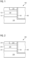
- FIG. 1 shows a schematic cross section of an embodiment of a silicon carbide device with a body region comprising at least two portions;
- FIG. 2 shows a schematic cross section of an embodiment of a silicon carbide device with a body region comprising at least three portions;
- FIG. 3 shows a flow chart of a method for forming a silicon carbide device according to an embodiment
- FIG. 4 shows a schematic cross section of an embodiment of a silicon carbide device with a spacer region
- FIG. 5 shows a schematic doping profile of a silicon carbide device according to an embodiment.
- a space-charge region may penetrate into body regions of transistors so that drain-induced barrier lowering may occur at these transistors.
- the short-channel effect may significantly influence a threshold voltage of the transistors and may impair an electrical characteristic of the silicon carbide device.
- FIG. 1 shows a schematic cross section of a silicon carbide device 100 according to an ex-emplary embodiment.
- the silicon carbide device 100 may comprise a transistor cell.
- the transistor cell may comprise a front side doping region 110 having a first conductivity type.
- the front side doping region 110 may be a source region or a drain region of the transistor cell.
- the front side doping region 110 may be located within a silicon carbide substrate of the silicon carbide device 100 , for example adjacent to a surface of the silicon carbide substrate.
- an upper surface of the front side doping region 110 may form a part of the surface of the silicon carbide substrate.
- the transistor cell may comprise a body region 120 having a second conductivity type.
- the second conductivity type may be the opposite conductivity type of the first conductivity type.
- the first conductivity type may be an n-type resulting in an n-doped region and the second conductivity type may be a p-type resulting in a p-doped region, or vice versa.
- the transistor cell may comprise a drift region 130 , e.g. having the first conductivity type.
- the drift region 130 may be located adjacent to the body region 120 so that a pn-junction exists between the body region 120 and the drift region 130 .
- the body region 120 may be located between the front side doping region 110 and the drift region 130 , e.g. in a vertical direction. Alternatively, the body region 120 may be located between the front side doping region 110 and the drift region 130 in a direction differing from a vertical direction by at most 8 degrees, for example at least 2 degrees and/or at most 6 degrees (e.g. by 4 degrees) (e.g. in case of a vertical transistor cell) The body region 120 may be located adjacent to the front side doping region 110 so that a pn-j unction exists between the body region 120 and the front side doping region 110 .
- a vertical direction and a vertical dimension or thicknesses of layers may be measured orthogonal to a front side surface and/or a back side surface of the silicon carbide substrate.
- the transistor cell of the silicon carbide device 100 may be a vertical transistor cell and the front side doping region 110 , the body region 120 , and the drift region 130 may be arranged vertically (e.g., in a stacked manner or one above the other) within the silicon carbide substrate.
- FIG. 1 shows additionally a gate trench with a gate insulation layer 150 and a gate electrode 160 in the trench for a vertical transistor cell.
- the body region 120 may comprise several doping portions.
- the body region 120 may comprise a first portion 121 , e.g. having a first average net doping concentration.
- the body region 120 may comprise a second portion 122 , e.g. having a second average net doping concentration.
- the first portion 121 may be located between the drift region 130 and the second portion 122 .
- the first portion 121 may be located between the drift region 130 and the second portion 122 in the vertical direction.
- the first portion 121 of the body region 120 may have an extension of at least 50 nm (or of at least 70 nm, of at least 100 nm, of at least 150 nm, or of at least 200 nm) within the body region 120 , e.g. in the vertical direction or in the direction differing from a vertical direction by at most 8 degrees.
- the second portion 122 of the body region 120 may have an extension of at least 50 nm (or of at least 100 nm, of at least 200 nm, or of at least 300 nm) within the body region 120 in the vertical direction or in the direction differing from a vertical direction by at most 8 degrees.
- an extension of a portion of a doped region for example a portion of the body region, may be the full width at half maximum (FWHM) of said portion.
- the vertical direction may extend from the front side doping region 110 to the drift region 130 .
- the direction from the front side doping region 110 to the drift region 130 and/or the vertical direction may be a direction in parallel to an interface between the body region 120 and a gate insulation layer 150 of the transistor cell.
- the first portion 121 of the body region may have an extension of at most 300 nm (or at most 200 nm, or at most 150 nm) in the vertical direction and/or in the direction parallel to the interface between the body region 120 and the gate insulation layer 150 .
- the direction of extension may be a vertical direction or may differ from a vertical direction by at least 2 degrees and/or at most 6 degrees (e.g. by 4 degrees), e.g. if the interface is tilted with respect to the vertical direction.
- the first portion 121 may have a mainly vertical extension of at least 50 nm, if the transistor cell is a vertical transistor cell.
- the second average net doping concentration may differ from the first average net doping concentration.
- the first average net doping concentration may be at least two times (or at least three times, at least five times, or at least 10 times) the second average net doping concentration and/or at most 20 times (or at most 10 times) the second average net doping concentration.
- the first average net doping concentration may be at least 1 ⁇ 10 17 cm ⁇ 3 (or at least 3 ⁇ 10 17 cm ⁇ 3 , or at least 7 ⁇ 10 18 cm ⁇ 3 ) and/or at most 2 ⁇ 10 18 cm ⁇ 3 (or at most 8 ⁇ 10 17 cm ⁇ 3 , or at most 5 ⁇ 10 18 cm ⁇ 3 ).
- the first portion 121 with a relatively small extension may provide a fieldstop against penetration of a space-charge region from the drift region 130 into the body region 120 of the transistor cell during operation. Consequently, drain induced barrier lowering may be reduced within the transistor of the silicon carbide device 100 , for example. A reduction of the threshold voltage of the transistor may be avoided or reduced. For example, a switching characteristic of the transistor or the transistor cell of the silicon carbide device 100 may be improved by providing the first portion 121 .
- the transistor cell may comprise a gate insulation layer. At least the second portion 122 of the body region 120 may be located adjacent to and/or in contact with the gate insulation layer 150 of the transistor cell.
- the first portion 121 of the body region 120 may be located adjacent (e.g., directly adjacent) to and/or in contact with the gate insulation layer 150 of the transistor cell.
- a spacer region (not depicted in the embodiment of FIG. 1 ) may be located between the first portion of the body region 120 and the gate insulation layer 150 of the transistor cell. The spacer region may separate the first portion 121 from the gate insulation layer 150 . By providing the spacer region, a direct contact between the first portion 121 of the body region 120 and the gate insulation layer may be avoided. By keeping the first portion 121 of the body region 120 separated from the gate insulation layer, an influence of the first portion 121 on the threshold voltage of the transistor may be kept low.
- the spacer region may be a doped region having the first conductivity type.
- the spacer region is a portion of a common doping region of the first conductivity type comprising the drift region as well.
- the spacer region may have a higher doping concentration than the drift region. That is to say, the spacer region may be a portion of a common doping region of the first conductivity type comprising the drift region as well, wherein the doping concentration is increased in said portion.
- the spacer region may have a doping concentration similar or identical to a doping concentration of a current spread region of the silicon carbide device.
- the spacer region may have the second conductivity type.
- an average net doping concentration of the spacer region may be lower than the first average net doping concentration.
- the average net doping concentration of the spacer region may be at most 50% (or at most 40%, or at most 30%) the first average net doping concentration.
- the average net doping concentration of the spacer region may differ from the second average net doping concentration by less than 10% of the second average net doping concentration.
- a distance (e.g. a minimal distance and/or a lateral distance) between the first portion 121 of the body region 120 and the gate insulation 150 layer may be at least 20 nm (or at least 50 nm, at least 100 nm, or at least 200 nm) and/or at most 500 nm (or at most 300 nm, or at most 200 nm).
- the distance between the first portion 121 and the gate insulation layer 150 may be caused by the spacer region between the first portion 121 and the gate insulation layer 150 .
- At least 80% (or at least 90%) of the doping atoms within the first portion 121 of the body region 120 may be at least one of aluminum atoms or gallium atoms.
- doping atoms may have an influence (e.g. an intended influence) onto an electrical characteristic of the transistor cell, for example.
- Doping atoms may be electrically active atoms, e.g. acting as donators and/or acceptors in an operating mode of the transistor cell. Diffusion of at least one of aluminum atoms or gallium atoms within the silicon carbide substrate may be negligible. Due to the absence of diffusion, a small height (or vertical extension) of the first portion 121 may be achieved, for example.
- At least 80% (or at least 90%) of the doping atoms within the second portion 122 of the body region 120 may be at least one of boron atoms, boron difluoride molecules, fluorine atoms or chlorine atoms.
- the channel mobility within the second portion 122 may be improved.
- the second portion 122 can be formed with a low number of implantations.
- fluorine e.g., from boron difluoride molecules or from fluorine atoms
- the silicon carbide device 100 may further comprise a third portion of the body region 120 (not depicted in the embodiment of FIG. 1 ).
- the third portion of the body region may have a third average net doping concentration.
- the third portion may have an extension of at least 50 nm within the body region, e.g. in the vertical direction or in a direction differing from a vertical direction by at most 8 degrees.
- the third portion of the body region 120 may be located between the second portion 122 of the body region 120 and the front side doping region 110 .
- the third portion may at least partially define the threshold voltage of the transistor cell of the silicon carbide device, for example.
- the threshold voltage may, however, also be defined by other portions or regions of the silicon carbide device, such as, e.g., the second portion.
- the third average net doping concentration may be higher than the first average net doping concentration.
- the third average net doping concentration may be at least two times (or at least three times, at least five times, or at least 10 times) the second average net doping concentration and/or at most 30 times (or at most 20 times or at most 10 times) the second average net doping concentration.
- the third average net doping concentration is at least 10 times and at most 20 times the second average net doping concentration.
- a higher third average net doping concentration in comparison to the second average net doping concentration may lead to an improved contact to the body region.
- a high third average net doping concentration may support suppression of an accidental switch-on due to a parasitic npn transistor in the case of a short circuit (so-called anti-latch-up).
- the third average net doping concentration may be lower than the first average net doping concentration. For example, this may be the case in an embodiment of a silicon carbide device comprising a doping region.
- Providing the third portion within the body region 120 may result in a well-shaped doping profile within the body region 120 from the first portion 121 to the third portion as the doping concentration of the intermediate second portion 122 may be lower than the doping concentration of the first portion 121 and the third portion.
- At least 80% (or at least 90%) of the doping atoms within the third portion of the body region may be at least one of boron atoms, boron difluoride molecules, fluorine atoms or chlorine atoms or at least 80% (or at least 90%) of the doping atoms within the third portion of the body region may be at least one of boron atoms or aluminum atoms. Boron atoms within the third portion may cause an improved stability of the threshold voltage of the transistor of the silicon carbide device 100 .
- a first maximum net doping concentration within the third portion of the body region may be implemented to be higher than a second maximum net doping concentration within the first portion of the body region, for example.
- the second maximum net doping concentration of the first portion 121 lower than the first maximum net doping concentration of the third portion, the first portion 121 might not, or not significantly, influence the threshold voltage of the transistor.
- the silicon carbide device 100 may comprise a current spread region (not depicted in the embodiment of FIG. 1 ), e.g. having the first conductivity type.
- the current spread region may be located between the body region 120 and the drift region 130 .
- An average net doping concentration of the current spread region may be at least two times an average net doping concentration of the drift region 130 .
- the current spread region may extend vertically over at least 200 nm (or at least 500 nm or at least 800 nm).
- the silicon carbide device 100 may further comprise a drain region of the transistor cell (not shown in the sections shown in the figures), e.g. having the first conductivity type, with an average net doping concentration of the drain region being at least 30 times or even at least 100 times the average net doping concentration of the drift region 130 , for example.
- the drain region may be located at a back side of the silicon carbide substrate. The back side may be opposite the front side.
- a buffer layer of the first conductivity type may be implemented between the drain layer and the drift zone.
- a thickness of the buffer layer may be at least 1 ⁇ m and at most 30 ⁇ m.
- a doping concentration of the buffer layer may be at least 1 ⁇ 10 17 cm ⁇ 3 and at most 8 ⁇ 10 18 cm ⁇ 3 .
- the transistor cell of the silicon carbide device may comprise a trench gate.
- the trench gate may comprise the gate electrode and the gate insulation layer located in a gate trench.
- a transistor e.g. transistor cell
- a first sidewall of the trench gate may adjoin the transistor cell.
- a second, opposite sidewall may be free of the transistor cell.
- the transistor cell of the silicon carbide device may be located on two sides of the trench gate so that a body region may be located at two opposite sides of the trench gate. For example, at least one portion of each body region may be contact with a respective sidewall of the trench gate, e.g. a gate insulation layer of the trench gate.
- a second electrode may be located at a bottom of the gate trench.
- the second electrode may be used to contact a shielding doping region located adjacent to and/or below a bottom of the trench.
- the shielding doping region may have the second conductivity type.
- the second electrode may be connected or connectable to a different voltage (e.g. source voltage) than the gate electrode (e.g. the source voltage).
- the transistor cell of the silicon carbide device 100 may be a transistor cell of a plurality of transistor cells of a transistor arrangement.
- a transistor cell may comprise one or more source regions (e.g. distributed or located along a gate), at least one body region and a gate (e.g. a trench gate located within a gate trench extending into the semiconductor substrate), for example,
- the transistor cells of the plurality of transistor cells may share a common (mutual) drift region and/or a common drain region (e.g. if the transistor cells are MOSFET cells) or a common collector region (e.g. if the transistor cells are IGBT cells).
- the transistor of the silicon carbide device 100 and/or the transistor arrangement may be a vertical transistor structure conducting current between a front side surface of the silicon carbide substrate and a back side surface of the silicon carbide substrate.
- the transistor arrangement of the silicon carbide device comprises a plurality of source doping regions connected to a source wiring structure, a plurality of gate electrodes or a gate electrode grid connected to a gate wiring structure and a back side drain metallization.
- the silicon carbide device 100 may be a power semiconductor device.
- a power semiconductor device or an electrical structure (e.g. the transistor cell of the silicon carbide device 100 ) of the power semiconductor device may have a breakdown voltage or blocking voltage of more than 100 V or more than 500 V or more than 1 kV.
- FIG. 2 shows a schematic cross section of a silicon carbide device 200 according to an embodiment.
- the silicon carbide device 200 may comprise a transistor cell, e.g. comprising a front side doping region 210 .
- the front side doping region 210 may have a first conductivity type.
- the transistor cell may comprise a body region 220 having a second conductivity type, and/or a drift region 230 having the first conductivity type.
- the body region 220 may be located between the front side doping region 210 and the drift region 230 , e.g. in a vertical direction.
- the body region 220 may comprise a first portion 221 , e.g. having a first average net doping concentration.
- the body region 220 may comprise a second portion 222 , e.g. having a second average net doping concentration, and/or a third portion 223 , e.g. having a third average net doping concentration.
- the first portion 221 may be located between the drift region 230 and the second portion 222 .
- the second portion 222 may be located between the first portion 221 and the third portion 223 .
- the first portion 221 and/or the second portion 222 and/or the third portion 223 may each have an extension of at least 50 nm in the vertical direction.
- the vertical direction may be a direction extending from the front side doping region to the drift region, for example.
- the first average net doping concentration may be at least two times the second average net doping concentration.
- the third average net doping concentration may be at least two times the second average net doping concentration.
- the third portion 223 may be located adjacent to the front side doping region 210 , for example.
- the first portion 221 , the second portion 222 , and the third portion 223 may be arranged vertically within the body region 220 , e.g. as vertical stack, e.g. in a vertical transistor of the silicon carbide device 200 .
- the first average net doping concentration may be at least two times the second average net doping concentration.
- the third average net doping concentration may be at least two times the second average net doping concentration.
- FIG. 2 may comprise one or more optional ad-ditional features corresponding to one or more aspects mentioned in connection with the proposed concept of one or more embodiments described above or below (e.g. FIG. 1 or 3-5 ).
- Some embodiments relate to semiconductor devices with a transistor comprising a body region as described with respect to FIG. 1 or FIG. 2 .
- the body region may be provided in another wide band gap semiconductor substrate instead of silicon carbide.
- a wide band gap semiconductor substrate may have a band gap larger than 2 eV, for example larger than 3 eV.
- the wide band gap semiconductor substrate may be a diamond (C) substrate, a gallium nitride (GaN)-based semiconductor substrate.
- FIG. 3 shows a flow chart of a method 300 for forming a silicon carbide device according to an embodiment.
- the method 300 may be used to form embodiments of a silicon carbide device as described herein.
- the method 300 may comprise implanting 310 first dopants into a silicon carbide substrate with a first implantation dose to form a first portion of a body region of a transistor of the silicon carbide device.
- the first portion of the body region may have an extension of at least 50 nm within the body region in a vertical direction, e.g. a direction from a front side doping region of the transistor to a drift region of the transistor.
- the method 300 may comprise implanting 320 second dopants into the silicon carbide substrate with a second implantation dose to form a second portion of the body region.
- the second portion may be formed adjacent to the first portion.
- the second portion of the body region may have an extension of at least 50 nm within the body region.
- the first implantation dose may be at least two times the second implantation dose.
- the first implantation dose may be at least 2 ⁇ 10 12 cm ⁇ 2 .
- the implantation doses may be adapted according to an extension of the doping portions, e.g. the implantation doses may be selected so that a doping concentration of the first portion is at least two times a doping concentration of the second portion.
- the method 300 may further comprise forming a front side doping region of the transistor adjacent to the body region.
- the front side doping region may have the first conductivity type.
- the first portion of the body region may have an extension of at least 30 nm within the body region in a direction from the front side doping region to a drift region of the transistor.
- the first dopants are implanted with a first implantation energy higher than a second implantation energy used for implanting the second dopants.
- a third portion of the body region may be formed by implanting third dopants into the silicon carbide substrate with a third implantation energy lower than the second implantation energy.
- a third implantation energy lower than the second implantation energy.
- one or more implantation processes may be performed, e.g. with different implantation energies and/or different implantation doses.
- the method 300 may comprise forming 330 a mask for implanting the first dopants so that the first portion of the body region is formed at a distance from a gate insulation layer of the transistor.
- the forming 330 the mask may be performed before implanting the first dopants.
- the first portion of the body region may be formed with a minimal distance to the gate insulation layer of at least 20 nm (or at least 50 nm) and/or at most 500 nm (or at most 300 nm).
- FIG. 3 may comprise one or more optional ad-ditional features corresponding to one or more aspects mentioned in connection with the proposed concept of one or more embodiments described above or below (e.g. FIG. 1-2 or 4-5 ).
- FIG. 4 shows a schematic cross section of a silicon carbide device 490 .
- the silicon carbide device 490 of FIG. 4 is depicted as an n-channel transistor device, a p-channel transistor device can also be implemented, e.g. by changing the respective doping types from n to p and vice versa.
- the silicon carbide device 490 may be implemented similar to the implementation described in connection with FIG. 1 and/or FIG. 2 .
- the silicon carbide device 490 comprises a transistor comprising a body region located vertically between a front side doping region 480 (which can be a highly n-doped source region 480 ) and a lightly n-doped drift region and/or a current spread region n 2 .
- the body region comprises a first portion p 1 (e.g. fieldstop), a second portion p 2 , and an optional third portion p 3 implemented as described in connection with FIG. 1 and/or FIG. 2 .
- the silicon carbide device 490 comprises a trench gate with a gate trench.
- a gate insulation layer 412 of the trench gate is located between the body region and a gate electrode 410 located in the gate trench.
- a current flow through a channel region 470 of the transistor may be controlled by a gate voltage applied to the gate electrode 410 .
- a spacer region 400 may be located laterally between the first portion p 1 of the body region and the gate insulation layer 412 .
- a highly p-doped region 460 of the silicon carbide device may be located adjacent to the gate insulation layer 412 at a second side wall of the gate structure opposite to a first side wall of the trench gate located adjacent to the body region of the transistor.
- the highly p-doped region 460 extends from the bottom of the trench gate along the second side wall of the trench gate to a highly n-doped region 420 and/or to the front side surface.
- a highly p-doped shielding region 462 may be located at the bottom of the gate trench. The highly p-doped shielding region 462 may be in contact with or part of the highly p-doped region 460 .
- the highly n-doped region 420 may extend along the second side wall of the trench gate from the highly p-doped region 460 to the front side surface of the silicon carbide substrate.
- the highly n-doped region 420 may be formed simultaneously with the front side doping region 480 .
- the highly n-doped region 420 may be electrically connected to the front side doping region 480 .
- FIG. 4 may comprise one or more optional ad-ditional features corresponding to one or more aspects mentioned in connection with the proposed concept of one or more embodiments described above or below (e.g. FIG. 1-3 or 5 ).
- FIG. 5 shows a schematic doping profile 500 of a silicon carbide device.
- the doping profile 500 shows the net doping concentrations of donors ND and acceptors NA over depth WB within different regions of a silicon carbide device (e.g. along a cross section 450 shown in FIG. 4 ).
- the doping profile 500 is a vertical doping profile.
- the doping profile shown in FIG. 5 may be optimized with respect to an n-channel silicon carbide (SiC) based device with a p-type body region.
- SiC silicon carbide
- the doping profile 500 shows the relative doping concentrations in the front side doping region 510 (e.g., an n-type source region or n+ source 512 ), the body region 520 , a current spread region 522 (which may be n-doped) and a drift zone 532 (which may be n-doped) of a transistor.
- the body region 520 is p-doped.
- the body region 520 may comprise three components (e.g. seen in the order from the front side along the vertical direction): a third portion p 3 (e.g. comprising boron atoms), a second portion p 2 (e.g. comprising boron atoms) and a first portion p 1 (e.g. comprising aluminum atoms and providing a fieldstop).
- the first portion p 1 of the body region may have a very short vertical extension.
- the first portion p 1 may have an effect similar to a field stop zone of the body region 520 , e.g. against the dynamic penetration of the space charge region of the silicon carbide device into the body region 520 .
- the first portion p 1 may comprise at least one of aluminum atoms or gallium atoms as doping atoms.
- the second portion p 2 may have a medium vertical extension.
- the second portion p 2 may basically define the channel resistance.
- the second portion p 2 has a lower doping concentration than the first portion p 1 .
- the second portion may, for example, comprise boron as doping atoms.
- the third portion p 3 may have a relatively narrow vertical extension.
- the third portion p 3 may, at least partially, define the threshold voltage.
- the third portion p 3 may reduce a resistive path for holes in the case of high-energy short circuit and/or avalanche, thus supporting suppression of turn-on of a parasitic npn transistor.
- the third portion p 3 has a higher doping concentration than the second portion p 2 and may be formed by a boron implantation.
- the first portion may be realized by implanting aluminum as doping atoms, which may act as acceptor atoms. Aluminum atoms may show a negligible diffusion. Therefore, it may be possible to realize a short vertical extension of the first portion.
- the vertical half width of the first portion i.e. the FWHM of the first portion in the vertical direction
- the implantation dose may be scaled so that the penetration of a space charge region is pre-vented effectively.
- the implantation dose may be in a range between 1 ⁇ 10 12 and 5 ⁇ 10 13 atoms per cm 2 , typically between 2 ⁇ 10 12 and 2 ⁇ 10 13 atoms per cm 2 .
- a narrow first portion e.g., a narrow field stop region
- the diffusion in subsequent process acts which might not be negligible.
- the first portion may extend up to the gate insulation layer without influencing the threshold voltage. If the maximum doping concentration of the first portion exceeds the maximum doping concentration of the third portion, however, a certain spacing (e.g. via the spacer region) between the first portion and the gate insulation layer may be provided to prevent an influence of the first portion on the threshold voltage.
- a lateral width of the spacer region may be in a range between at least 20 nm and at most 500 nm, typically between at least 50 nm and at most 300 nm.
- the second portion of the body region may be implemented by a boron doping.
- the boron doping may, to a certain extent, also extend into the drift region.
- a boron doping may result in several effects: (i) Less implantation acts may be required, as during subsequent high-temperature processes a diffusion of boron (which might not be negligible) may lead to vertical smearing of the implantation profile. (ii) Additionally, in a boron doped region, an improved channel mobility may be obtained. (iii) Further, the boron doping (e.g.
- the second portion may also contain at least one of aluminum atoms or gallium atoms as doping atoms.
- the third portion of the body region may comprise aluminum atoms as doping atoms either alone or, in some examples, in combination with boron atoms and/or gallium atoms.
- boron is used as a dopant for the third portion, but a substantial part of the doping atoms in this zone may be aluminum atoms.
- the use of boron may bring a further effect regarding the stability of the threshold voltage: during processing of the silicon carbide substrate, hydrogen may be introduced into the semiconductor and acceptor-hydrogen complexes may form. This may lead to an instability of the threshold voltage if said complexes are dissolved due to current or temperature.
- an increased stability of the threshold voltage in operation may be achieved with boron as a doping atom.
- boron difluoride (BF2) molecules may be used, for example as doping atoms in the second portion.
- Fluorine may have the characteristic of being able to saturate “dangling bonds” at the interface between the gate insulation layer and the silicon carbide substrate in a stable and efficient way. Dangling bonds saturated by hydrogen may be less stable under stress, like e.g. increased temperature and/or high current densities.
- Fluorine for example boron difluoride
- the silicon carbide device may thus be free of a first portion in the bode region.
- the second portion and/or the third portion may be present, wherein the second portion and/or the third portion comprise fluorine as doping atoms.
- fluorine atoms or chlorine atoms may alternatively or additionally be exploited as ions not containing boron, preferably by implantation into the substrate surface.
- FIG. 5 may comprise one or more optional ad-ditional features corresponding to one or more aspects mentioned in connection with the proposed concept of one or more embodiments described above or below (e.g. FIGS. 1-4 ).
- Examples relate to concepts for reducing drain induced barrier lowering or short-channel effects in silicon carbide devices. It may be desired to minimize the penetration of the space charge region into the p-body of silicon carbide based devices during operation of these devices. This way, drain induced barrier lowering (DIBL) may be significantly reduced. An excessive drain induced barrier lowering may decrease the threshold voltage of the device too much in case of a high drain-source voltage. This may cause high short-circuit currents with a DC link voltage close to an application voltage, for example. Further, in some embodiments, a switch-off performance may be influenced undesired, as with highly inductive switching with high overvoltage drain induced barrier lowering may cut off the channel faster. The device may switch “more aggressively” and strong successive LC oscillations may occur. This may be critical, for example, for high-voltage silicon carbide devices which have to switch high currents in a high parallel switching degree.
- a deep p shielding structure may be implemented more narrow (p-hole reduction), but this may cause a strong increase of the R DS,on .
- an improved (e.g. softer) switching performance on the customer size may be achieved, for example, when high current applications are used with highly inductive circuits (e.g. traction applications).
- a normal 1-stage gate driver which may be used for IGBTs may be applicable by using proposed concepts.
- a low short-circuit current may be achieved which may increase the short circuit ro-bustness.
- Examples relate to the realization of a special doping profile (e.g. the doping profile shown in FIG. 5 ) for silicon carbide based devices, which may counteract, for example, the penetration of the space charge region into the p-body during operation of the device.
- a special doping profile e.g. the doping profile shown in FIG. 5
- silicon carbide based devices which may counteract, for example, the penetration of the space charge region into the p-body during operation of the device.
- the proposed concepts may be detected by using doping profile analyses by means of spreading resistance measurements or secondary-ion mass spectrometry SIMS analyses.
- the proposed concepts may be applied to various power semiconductor devices, for example.
- each claim may stand on its own as a separate example. While each claim may stand on its own as a separate example, it is to be noted that—although a dependent claim may refer in the claims to a specific combination with one or more other claims—other examples may also include a combination of the dependent claim with the subject matter of each other dependent or independent claim. Such combinations are explicitly proposed herein unless it is stated that a specific combination is not intended. Furthermore, it is intended to include also features of a claim to any other independent claim even if this claim is not directly made dependent to the independent claim.
Landscapes
- Electrodes Of Semiconductors (AREA)
- Junction Field-Effect Transistors (AREA)
- Recrystallisation Techniques (AREA)
Abstract
Description
Claims (23)
Applications Claiming Priority (2)
| Application Number | Priority Date | Filing Date | Title |
|---|---|---|---|
| DE102018123210.1 | 2018-09-20 | ||
| DE102018123210.1A DE102018123210B3 (en) | 2018-09-20 | 2018-09-20 | Silicon carbide devices and method for forming silicon carbide devices |
Publications (2)
| Publication Number | Publication Date |
|---|---|
| US20200098869A1 US20200098869A1 (en) | 2020-03-26 |
| US11264464B2 true US11264464B2 (en) | 2022-03-01 |
Family
ID=69412874
Family Applications (1)
| Application Number | Title | Priority Date | Filing Date |
|---|---|---|---|
| US16/576,042 Active US11264464B2 (en) | 2018-09-20 | 2019-09-19 | Silicon carbide devices and methods for forming silicon carbide devices |
Country Status (3)
| Country | Link |
|---|---|
| US (1) | US11264464B2 (en) |
| CN (1) | CN110931562B (en) |
| DE (1) | DE102018123210B3 (en) |
Families Citing this family (2)
| Publication number | Priority date | Publication date | Assignee | Title |
|---|---|---|---|---|
| DE102019121859B3 (en) * | 2019-08-14 | 2020-11-26 | Infineon Technologies Ag | SILICON CARBIDE DEVICE WITH TRENCH GATE |
| US12604504B2 (en) | 2021-11-23 | 2026-04-14 | Infineon Technologies Ag | Shielding structure for silicon carbide devices |
Citations (3)
| Publication number | Priority date | Publication date | Assignee | Title |
|---|---|---|---|---|
| US20160247884A1 (en) * | 2015-02-24 | 2016-08-25 | Kabushiki Kaisha Toshiba | Semiconductor device and method for manufacturing the same |
| US9773883B2 (en) * | 2014-02-17 | 2017-09-26 | Toyota Jidosha Kabushiki Kaisha | Method for manufacturing insulated gate type switching device having low-density body region and high-density body region |
| US20180097079A1 (en) * | 2016-10-05 | 2018-04-05 | Fuji Electric Co., Ltd. | Semiconductor device and method of manufacturing semiconductor device |
Family Cites Families (6)
| Publication number | Priority date | Publication date | Assignee | Title |
|---|---|---|---|---|
| GB9313843D0 (en) * | 1993-07-05 | 1993-08-18 | Philips Electronics Uk Ltd | A semiconductor device comprising an insulated gate field effect transistor |
| JP6048317B2 (en) * | 2013-06-05 | 2016-12-21 | 株式会社デンソー | Silicon carbide semiconductor device |
| CN108352402B (en) * | 2015-10-16 | 2020-12-18 | 富士电机株式会社 | Semiconductor device and manufacturing method of semiconductor device |
| JP6115678B1 (en) * | 2016-02-01 | 2017-04-19 | 富士電機株式会社 | Silicon carbide semiconductor device and method for manufacturing silicon carbide semiconductor device |
| CN105845718B (en) * | 2016-05-19 | 2019-11-05 | 杭州电子科技大学 | A kind of 4H-SiC trench-type insulated gate bipolar transistor |
| JP6769165B2 (en) * | 2016-08-10 | 2020-10-14 | 富士電機株式会社 | Semiconductor device |
-
2018
- 2018-09-20 DE DE102018123210.1A patent/DE102018123210B3/en active Active
-
2019
- 2019-09-19 US US16/576,042 patent/US11264464B2/en active Active
- 2019-09-20 CN CN201910891488.4A patent/CN110931562B/en active Active
Patent Citations (3)
| Publication number | Priority date | Publication date | Assignee | Title |
|---|---|---|---|---|
| US9773883B2 (en) * | 2014-02-17 | 2017-09-26 | Toyota Jidosha Kabushiki Kaisha | Method for manufacturing insulated gate type switching device having low-density body region and high-density body region |
| US20160247884A1 (en) * | 2015-02-24 | 2016-08-25 | Kabushiki Kaisha Toshiba | Semiconductor device and method for manufacturing the same |
| US20180097079A1 (en) * | 2016-10-05 | 2018-04-05 | Fuji Electric Co., Ltd. | Semiconductor device and method of manufacturing semiconductor device |
Also Published As
| Publication number | Publication date |
|---|---|
| CN110931562B (en) | 2026-02-24 |
| CN110931562A (en) | 2020-03-27 |
| DE102018123210B3 (en) | 2020-02-27 |
| US20200098869A1 (en) | 2020-03-26 |
Similar Documents
| Publication | Publication Date | Title |
|---|---|---|
| CN100524809C (en) | A field effect transistor semiconductor device | |
| US10700168B2 (en) | Wide band gap semiconductor device and a method for forming a wide band gap semiconductor device | |
| US8759935B2 (en) | Power semiconductor device with high blocking voltage capacity | |
| US8653556B2 (en) | Vertical semiconductor device | |
| US11164965B2 (en) | Semiconductor device | |
| US9219138B2 (en) | Semiconductor device having localized charge balance structure and method | |
| US20140306284A1 (en) | Semiconductor Device and Method for Producing the Same | |
| WO2021030490A1 (en) | High density power device with selectively shielded recessed field plate | |
| US9331194B2 (en) | Semiconductor device and method for manufacturing semiconductor device | |
| US11264464B2 (en) | Silicon carbide devices and methods for forming silicon carbide devices | |
| JP2023076986A (en) | Semiconductor device and its manufacturing method | |
| CN110504298B (en) | Silicon carbide semiconductor device | |
| KR102406116B1 (en) | Semiconductor device and method manufacturing the same | |
| JP7729880B2 (en) | Power semiconductor device and method of operation | |
| US11282926B2 (en) | Semiconductor device with a semiconductor body of silicon carbide | |
| JP2025089279A (en) | Semiconductor component and method for manufacturing semiconductor component | |
| CN119486219A (en) | A field effect transistor | |
| US10153339B2 (en) | Semiconductor device and method for forming a semiconductor device | |
| KR102335490B1 (en) | Semiconductor device and method manufacturing the same | |
| US20230163167A1 (en) | Semiconductor device including a trench gate structure | |
| KR20140092209A (en) | Semiconductor Power Rectifying Device | |
| US20250048700A1 (en) | Ultra-short channel lengths in sic mos-based power devices and method of making the same | |
| Rongyao et al. | Carrier stored trench-gate bipolar transistor with p-floating layer | |
| JP2024158011A (en) | Silicon carbide semiconductor device | |
| JP2024126206A (en) | Semiconductor Device |
Legal Events
| Date | Code | Title | Description |
|---|---|---|---|
| FEPP | Fee payment procedure |
Free format text: ENTITY STATUS SET TO UNDISCOUNTED (ORIGINAL EVENT CODE: BIG.); ENTITY STATUS OF PATENT OWNER: LARGE ENTITY |
|
| STPP | Information on status: patent application and granting procedure in general |
Free format text: NON FINAL ACTION MAILED |
|
| AS | Assignment |
Owner name: INFINEON TECHNOLOGIES AG, GERMANY Free format text: ASSIGNMENT OF ASSIGNORS INTEREST;ASSIGNORS:SCHULZE, HANS-JOACHIM;BASLER, THOMAS;STEGNER, ANDRE RAINER;SIGNING DATES FROM 20190918 TO 20210112;REEL/FRAME:054891/0894 |
|
| STPP | Information on status: patent application and granting procedure in general |
Free format text: NON FINAL ACTION MAILED |
|
| STPP | Information on status: patent application and granting procedure in general |
Free format text: RESPONSE TO NON-FINAL OFFICE ACTION ENTERED AND FORWARDED TO EXAMINER |
|
| STPP | Information on status: patent application and granting procedure in general |
Free format text: FINAL REJECTION MAILED |
|
| STPP | Information on status: patent application and granting procedure in general |
Free format text: RESPONSE AFTER FINAL ACTION FORWARDED TO EXAMINER |
|
| STPP | Information on status: patent application and granting procedure in general |
Free format text: NOTICE OF ALLOWANCE MAILED -- APPLICATION RECEIVED IN OFFICE OF PUBLICATIONS |
|
| STCF | Information on status: patent grant |
Free format text: PATENTED CASE |
|
| MAFP | Maintenance fee payment |
Free format text: PAYMENT OF MAINTENANCE FEE, 4TH YEAR, LARGE ENTITY (ORIGINAL EVENT CODE: M1551); ENTITY STATUS OF PATENT OWNER: LARGE ENTITY Year of fee payment: 4 |