US11264422B2 - Scalable position-sensitive photodetector device - Google Patents
Scalable position-sensitive photodetector device Download PDFInfo
- Publication number
- US11264422B2 US11264422B2 US16/557,149 US201916557149A US11264422B2 US 11264422 B2 US11264422 B2 US 11264422B2 US 201916557149 A US201916557149 A US 201916557149A US 11264422 B2 US11264422 B2 US 11264422B2
- Authority
- US
- United States
- Prior art keywords
- photodetectors
- photodetector
- array
- electrically coupled
- horizontal
- Prior art date
- Legal status (The legal status is an assumption and is not a legal conclusion. Google has not performed a legal analysis and makes no representation as to the accuracy of the status listed.)
- Expired - Fee Related, expires
Links
Images


Classifications
-
- H01L27/14643—
-
- G—PHYSICS
- G01—MEASURING; TESTING
- G01S—RADIO DIRECTION-FINDING; RADIO NAVIGATION; DETERMINING DISTANCE OR VELOCITY BY USE OF RADIO WAVES; LOCATING OR PRESENCE-DETECTING BY USE OF THE REFLECTION OR RERADIATION OF RADIO WAVES; ANALOGOUS ARRANGEMENTS USING OTHER WAVES
- G01S7/00—Details of systems according to groups G01S13/00, G01S15/00, G01S17/00
- G01S7/48—Details of systems according to groups G01S13/00, G01S15/00, G01S17/00 of systems according to group G01S17/00
- G01S7/481—Constructional features, e.g. arrangements of optical elements
- G01S7/4816—Constructional features, e.g. arrangements of optical elements of receivers alone
-
- H—ELECTRICITY
- H10—SEMICONDUCTOR DEVICES; ELECTRIC SOLID-STATE DEVICES NOT OTHERWISE PROVIDED FOR
- H10F—INORGANIC SEMICONDUCTOR DEVICES SENSITIVE TO INFRARED RADIATION, LIGHT, ELECTROMAGNETIC RADIATION OF SHORTER WAVELENGTH OR CORPUSCULAR RADIATION
- H10F39/00—Integrated devices, or assemblies of multiple devices, comprising at least one element covered by group H10F30/00, e.g. radiation detectors comprising photodiode arrays
- H10F39/10—Integrated devices
- H10F39/12—Image sensors
- H10F39/18—Complementary metal-oxide-semiconductor [CMOS] image sensors; Photodiode array image sensors
-
- G—PHYSICS
- G01—MEASURING; TESTING
- G01S—RADIO DIRECTION-FINDING; RADIO NAVIGATION; DETERMINING DISTANCE OR VELOCITY BY USE OF RADIO WAVES; LOCATING OR PRESENCE-DETECTING BY USE OF THE REFLECTION OR RERADIATION OF RADIO WAVES; ANALOGOUS ARRANGEMENTS USING OTHER WAVES
- G01S7/00—Details of systems according to groups G01S13/00, G01S15/00, G01S17/00
- G01S7/48—Details of systems according to groups G01S13/00, G01S15/00, G01S17/00 of systems according to group G01S17/00
- G01S7/483—Details of pulse systems
- G01S7/486—Receivers
- G01S7/4861—Circuits for detection, sampling, integration or read-out
- G01S7/4863—Detector arrays, e.g. charge-transfer gates
-
- H01L27/1446—
-
- H01L27/14601—
-
- H01L31/107—
-
- H—ELECTRICITY
- H10—SEMICONDUCTOR DEVICES; ELECTRIC SOLID-STATE DEVICES NOT OTHERWISE PROVIDED FOR
- H10F—INORGANIC SEMICONDUCTOR DEVICES SENSITIVE TO INFRARED RADIATION, LIGHT, ELECTROMAGNETIC RADIATION OF SHORTER WAVELENGTH OR CORPUSCULAR RADIATION
- H10F30/00—Individual radiation-sensitive semiconductor devices in which radiation controls the flow of current through the devices, e.g. photodetectors
- H10F30/20—Individual radiation-sensitive semiconductor devices in which radiation controls the flow of current through the devices, e.g. photodetectors the devices having potential barriers, e.g. phototransistors
- H10F30/21—Individual radiation-sensitive semiconductor devices in which radiation controls the flow of current through the devices, e.g. photodetectors the devices having potential barriers, e.g. phototransistors the devices being sensitive to infrared, visible or ultraviolet radiation
- H10F30/22—Individual radiation-sensitive semiconductor devices in which radiation controls the flow of current through the devices, e.g. photodetectors the devices having potential barriers, e.g. phototransistors the devices being sensitive to infrared, visible or ultraviolet radiation the devices having only one potential barrier, e.g. photodiodes
- H10F30/225—Individual radiation-sensitive semiconductor devices in which radiation controls the flow of current through the devices, e.g. photodetectors the devices having potential barriers, e.g. phototransistors the devices being sensitive to infrared, visible or ultraviolet radiation the devices having only one potential barrier, e.g. photodiodes the potential barrier working in avalanche mode, e.g. avalanche photodiodes
-
- H—ELECTRICITY
- H10—SEMICONDUCTOR DEVICES; ELECTRIC SOLID-STATE DEVICES NOT OTHERWISE PROVIDED FOR
- H10F—INORGANIC SEMICONDUCTOR DEVICES SENSITIVE TO INFRARED RADIATION, LIGHT, ELECTROMAGNETIC RADIATION OF SHORTER WAVELENGTH OR CORPUSCULAR RADIATION
- H10F39/00—Integrated devices, or assemblies of multiple devices, comprising at least one element covered by group H10F30/00, e.g. radiation detectors comprising photodiode arrays
- H10F39/10—Integrated devices
- H10F39/107—Integrated devices having multiple elements covered by H10F30/00 in a repetitive configuration, e.g. radiation detectors comprising photodiode arrays
-
- H—ELECTRICITY
- H10—SEMICONDUCTOR DEVICES; ELECTRIC SOLID-STATE DEVICES NOT OTHERWISE PROVIDED FOR
- H10F—INORGANIC SEMICONDUCTOR DEVICES SENSITIVE TO INFRARED RADIATION, LIGHT, ELECTROMAGNETIC RADIATION OF SHORTER WAVELENGTH OR CORPUSCULAR RADIATION
- H10F39/00—Integrated devices, or assemblies of multiple devices, comprising at least one element covered by group H10F30/00, e.g. radiation detectors comprising photodiode arrays
- H10F39/80—Constructional details of image sensors
-
- H—ELECTRICITY
- H10—SEMICONDUCTOR DEVICES; ELECTRIC SOLID-STATE DEVICES NOT OTHERWISE PROVIDED FOR
- H10F—INORGANIC SEMICONDUCTOR DEVICES SENSITIVE TO INFRARED RADIATION, LIGHT, ELECTROMAGNETIC RADIATION OF SHORTER WAVELENGTH OR CORPUSCULAR RADIATION
- H10F77/00—Constructional details of devices covered by this subclass
- H10F77/95—Circuit arrangements
- H10F77/953—Circuit arrangements for devices having potential barriers
- H10F77/957—Circuit arrangements for devices having potential barriers for position-sensitive photodetectors, e.g. lateral-effect photodiodes or quadrant photodiodes
Definitions
- the present application relates generally to position-sensitive photodetectors.
- Photodetectors are used to sense light or other electromagnetic radiation and have a variety of applications.
- One application of photodetectors is to determine the position of a light source, which can be useful in ladar, lidar, tracking, other optical remote sensing applications, and medical applications.
- Position can be determined according to the following equations:
- SiPM silicon photomultiplier
- SiPMs can be used to detect the optical output signal of scintillators, which are gamma-ray detectors that convert a high-energy gamma ray into a shower of photons.
- Quadrant detection can be used with SiPM photodetectors to achieve position sensitivity, but it is limited by the photosensitive area of the SiPMs (typically ⁇ 0.36 cm 2 /SiPM), so the total photosensitive area of a SiPM quadrant detector would be 4 ⁇ 0.36 cm 2 /SiPM or 1.44 cm 2 ).
- larger-area SiPMs could be fabricated; however, large-area SiPMs suffer from large capacitance (e.g., 5-50 nF/cm 2 ), and therefore low bandwidth and low signal amplitudes.
- the high capacitance distorts the inherently fast signals of the SiPM, which are commonly read out with 50-ohm high-performance RF amplifiers.
- the RC time constant is 250-2,500 ns/cm 2 , limiting the frequency response to 60-600 kHz/cm 2 .
- Fast timing performance generally requires high bandwidth, which limits the photosensitive area of the SiPM to much less than 1 cm 2 .
- Commonly-used SiPMs for high-performance timing use a SiPM size of 0.1-0.2 cm 2 .
- Some SiPM readout circuits also use a smaller termination resistance to improve the bandwidth, or they use various transimpedance amplifiers or bootstrap circuits to mitigate the high capacitance.
- a scintillator is a gamma-ray detector that converts the energy of a gamma ray into a shower of optical photons. Desirable properties of scintillator include high brightness (e.g., high numbers of optical photons for each gamma ray detected), fast rise times (e.g., rise time of the shower of optical photons) and fast decay times (e.g., decay of the shower of optical photons).
- Typical high-performance scintillators emit over 10,000 optical photons/MeV of gamma-ray energy, with picosecond rise times and nanosecond decay times.
- the scintillator is mated to a position-sensitive photodetector, which detects the shower of optical photons and provides the position of the shower within the scintillator (X,Y position), the time of the shower (usually triggered by the rising edge), and an estimation of the number of photons detected, which is used to estimate the energy of the gamma ray.
- the advantage of the Anger Camera is not simply in increasing the area of a gamma camera; it also addresses the issue of light sharing among the quadrants of a quadrant detector. As the area of a quadrant detector is increased, it becomes more likely that the light beam will no longer intersect all four photodetectors. Instead, nearly all of the light beam will only intersect one photodetector (e.g., as illustrated in FIG. 2A ), and position sensitivity degrades and may be lost completely.
- the Anger Camera solution breaks the quadrant detector into an array of photodetector elements (e.g., as illustrated in FIG. 2B ) so that for at least some section of the Anger Camera, the light is still divided between 4 or more photodetectors, and position sensitivity is regained.
- Examples of conventional Anger logic circuit connections include (a) resistive mesh connections ( FIG. 3 ), (b) capacitive mesh connections ( FIG. 4 ), and (c) hybrid mesh connections ( FIG. 5 ) of photodetectors 100 with current photocurrent outputs A-D.
- the anodes 105 (or cathodes) of photodetectors 100 are connected in rows 300 using a resistor 310 between the anode 105 (or cathode) of each photodetector 100 .
- the rows 300 of the photodetector array are connected to adjacent rows 300 at both ends using another resistor between each row 300 .
- the outputs A-D are at the corners of the array.
- the photodetector current is divided between each of the four corners in inverse proportion to the total resistance between the photodetector and the corner contact (e.g., as in a resistive divider).
- the anodes 105 (or cathodes) of photodetectors 100 are connected in rows 300 using a capacitor 420 between the anode 105 (or cathode) of each photodetector 100 .
- the rows 300 of the photodetector array are connected to adjacent rows 300 at both ends using another capacitor 420 between each row 300 .
- the outputs A-D are at the corners of the array. High-frequency photodetector current is divided between each of the four corners in direct proportion to the effective capacitance between the photodetector and each corner contact.
- capacitors 420 are electrically coupled in series, and assuming that all capacitors 420 have equal capacitance, a connection of 10 capacitors in series has 1/10th the impedance of a single capacitor.
- capacitive mesh connections generally also require a direct current path to ground at each node as well, since the circuit is AC coupled.
- the anodes 105 (or cathodes) of photodetectors 100 are connected in rows 300 using a parallel connection of a resistor 310 and a capacitor 420 between the anode 105 (or cathode) of each photodetector 100 .
- the rows 300 of the photodetector array are connected to adjacent rows 300 at both ends using another parallel-connected resistor 310 and capacitor 420 between each row 300 .
- the outputs A-D are at the corners of the array. Photodetector current is divided between each of the four corners in inverse proportion to the effective impedance between the photodetector and each corner contact.
- the equivalent circuit model for one row 300 of 4 photodetectors 100 using any of the conventional Anger logic connections in FIGS. 3-5 can be generalized as equivalent circuit 60 in FIG. 6 including the parallel resistor (R h ) and capacitor (C h ) connection, the capacitance of each photodetector 100 (C D ), the shunt resistance of each photodiode (R s ), and the photocurrent of each photodiode (I DN ).
- the photocurrent (I DN ) of each photodetector 100 is relatively independent and splits according to the effective impedance to outputs A and D, so the photocurrent on the left side (output A) does not need to equal the current on the right side (output D).
- each photodetector may also include an external resistor component. This is because many photodetectors have nearly infinite Rs, and for the capacitive mesh configuration it may be necessary to provide a DC path to ground, so an external shunt resistor is used.
- the currents split right/left based on the impedance ratio to contacts A and D.
- the conventional Anger Logic connection there are low-impedance paths through the photodetector capacitance C D of each element in the array to the common connection (ground in FIG. 7 ), which significantly reduces the current available for readout at contacts A and D.
- the current reduction caused by this low impedance path to the common connection for each photodetector limits scaling of conventional Anger logic to large arrays of photodetectors.
- positron emission tomography PET
- PET positron emission tomography
- a common PET tracer is fluorodeoxyglucose (FDG).
- FDG fluorodeoxyglucose
- the PET scanner detects the gamma rays given off by the FDG and produces images of the body that show both normal and cancerous tissue. Accurate localization of the X-Y position of the Gamma ray detection event is often achieved using an Anger Logic connection of photodetector elements.
- Modern commercial PET machines include the capability to measure time-of-flight.
- the FDG tracer emits positrons which annihilate and produce a pair of counter-propagating gamma rays.
- the PET machine uses coincidence detection between opposing gamma cameras to determine a line of response which ideally indicates that the FDG tracer was located somewhere along the line.
- Time-of-Flight PET uses the time difference of the detection event at the opposing gamma cameras to estimate more precisely where the FDG is located in position along the line of response.
- TOF-PET enables higher sensitivity to be achieved, enabling higher resolution images to be achieved at a lower radioactive dose to the patient. Therefore it is critical for TOF-PET applications that the gamma camera have the best possible timing performance. For example, timing resolution of less than 100 picoseconds would enable improved performance in TOF-PET applications.
- Example embodiments described herein have innovative features, no single one of which is indispensable or solely responsible for their desirable attributes.
- the following description and drawings set forth certain illustrative implementations of the disclosure in detail, which are indicative of several exemplary ways in which the various principles of the disclosure may be carried out.
- the illustrative examples, however, are not exhaustive of the many possible embodiments of the disclosure. Without limiting the scope of the claims, some of the advantageous features will now be summarized. Other objects, advantages and novel features of the disclosure will be set forth in the following detailed description of the disclosure when considered in conjunction with the drawings, which are intended to illustrate, not limit, the invention.
- An aspect of the invention is directed to a position-sensitive device comprising: a photodetector grid comprising: horizontal arrays of HA photodetectors, the HA photodetectors in each horizontal array electrically coupled in series to each other; and vertical arrays of VA photodetectors, the VA photodetectors in each vertical array electrically coupled in series to each other; a vertical output line electrically coupled to each horizontal array of HA photodetectors; a horizontal output line electrically coupled to each vertical array of VA photodetectors, wherein the HA and VA photodetectors are arranged in an alternating sequence to form the photodetector grid.
- the photodetector grid comprises rows and columns
- the HA and VA photodetectors in each row comprise the HA photodetectors from one of the horizontal arrays and individual VA photodetectors from different respective vertical arrays to form the alternating sequence of the HA and VA photodetectors along the row
- the HA and VA photodetectors in each column comprise the VA photodetectors from one of the vertical arrays and individual HA photodetectors from different respective horizontal arrays to form the alternating sequence of the HA and VA photodetectors along the column.
- the HA photodetectors in adjacent horizontal arrays are positionally-offset along a horizontal axis
- the VA photodetectors in adjacent vertical arrays are positionally-offset along a vertical axis.
- the HA and VA photodetectors are arranged in a checkerboard configuration.
- the photodetector grid comprises rows and columns, and each column includes the VA photodetectors from a corresponding vertical array and individual HA photodetectors from different respective horizontal arrays.
- a first group of rows includes the HA photodetectors from a corresponding horizontal array, and a second group of rows includes individual VHA photodetectors from different respective vertical arrays.
- a shunt resistor is electrically coupled in parallel with each HA photodetector and in parallel with each VA photodetector.
- the device further comprises passive circuit elements electrically coupled to the vertical output line, wherein each horizontal array has a horizontal array termination that is electrically coupled to the vertical output line, the passive circuit elements and the horizontal array terminations in an alternating arrangement along the vertical output line.
- the device further comprises first and second outputs at opposing ends of the vertical output line and one of the passive circuit elements is electrically coupled to the vertical output line between the first output and a first outermost horizontal array termination and another of the passive circuit elements is electrically coupled to the vertical output line between the second output and a last outermost horizontal array termination.
- each passive circuit element comprises a resistor, a capacitor, and/or an inductor.
- each passive circuit element comprises a resistor electrically disposed in parallel with a capacitor.
- the device further comprises passive circuit elements electrically coupled to the horizontal output line, wherein each vertical array has a vertical array termination that is electrically coupled to the horizontal output line, the passive circuit elements and the vertical array terminations in an alternating arrangement along the horizontal output line.
- the device further comprises first and second outputs at opposing ends of the horizontal output line and one of the passive circuit elements is electrically coupled to the horizontal output line between the first output and a first outermost vertical array termination and another of the passive circuit elements is electrically coupled to the horizontal output line between the second output and a last outermost vertical array termination.
- terminations of the vertical and horizontal arrays are electrically coupled to a common output.
- the device further comprises an RF amplifier that is electrically coupled between the terminations and the common output.
- the HA photodetectors are the VA photodetectors are the same type of photodetector.
- the device further comprises the HA photodetectors and the VA detectors comprise silicon photomultipliers, PIN photodiodes, PN diodes, photoconductors, and/or avalanche photodiodes.
- FIGS. 1A, 1B, and 2A are schematic diagrams of quadrant photodetectors according to the prior art.
- FIG. 2B is a schematic diagram of an array of photodetectors according to the prior art.
- FIG. 3 is a schematic diagram of an array of photodetectors having resistive mesh connections according to the prior art.
- FIG. 4 is a schematic diagram of an array of photodetectors having capacitive mesh connections according to the prior art.
- FIG. 5 is a schematic diagram of an array of photodetectors having hybrid mesh connections according to the prior art.
- FIG. 6 is a generalized circuit diagram for the equivalent circuit of one row for the schematic diagrams of FIGS. 3-5 .
- FIG. 7 illustrates the generalized circuit diagram of FIG. 6 when one of the photodetectors is triggered.
- FIGS. 8 and 9 are schematic diagrams of a position-sensitive device according to one or more embodiments.
- FIG. 10 is a schematic diagram of one row (or column) of a representative photodetector array according to one or more embodiments.
- FIG. 11 is a circuit diagram of the equivalent circuit formed the representative photodetector array illustrated in FIG. 10 .
- FIG. 12 illustrates the circuit diagram of FIG. 11 when one of the photodetectors is triggered.
- FIG. 13 is a schematic electrical diagram of a representative photodetector array according to an alternative embodiment.
- FIG. 14 is a schematic diagram of a position-sensitive device according to one or more embodiments.
- FIG. 15 is a simplified schematic diagram of a photodetector grid to illustrate the detection of a photon beam.
- FIG. 16 is a schematic diagram of a position-sensitive photodetector device according to an alternative embodiment.
- FIG. 17 is a block diagram of a position-sensitive photodetection system according to one or more embodiments.
- a position-sensitive photodetector device includes a grid of series-connected photodetectors that are electrically coupled to either a vertical photodetector array (VA photodetectors) or to a horizontal photodetector array (HA photodetectors).
- VA photodetectors vertical photodetector array
- HA photodetectors horizontal photodetector array
- the VA and HA photodetectors are arranged in an alternating sequence within rows and/or columns of photodetectors in the grid.
- the grid has a checkerboard configuration. In the checkerboard configuration, each row includes all of the HA photodetectors from one of the horizontal photodetector arrays and separate VA photodetectors from different vertical photodetector arrays.
- each column includes all of the VA photodetectors from one of the vertical photodetector arrays and separate HA photodetectors from different horizontal photodetector arrays.
- the grid has a striped configuration.
- alternating rows include either only HA photodetectors or only VA photodetectors.
- a first group of rows only includes HA photodetectors from each of a corresponding horizontal photodetector array.
- a second group of rows only includes an individual VA photodetector from different respective vertical photodetector arrays.
- Each column includes VA photodetectors from a corresponding vertical photodetector array and an individual HA photodetector from different respective horizontal photodetector arrays.
- the grid can have a vertically-striped configuration where alternating columns include either only HA photodetectors or only VA photodetectors.
- a first group of columns only includes VA photodetectors from each of a corresponding vertical photodetector array.
- a second group of columns only includes an individual HA photodetector from different respective horizontal photodetector arrays.
- Each row includes HA photodetectors from a corresponding horizontal photodetector array and an individual VA photodetector from different respective vertical photodetector arrays.
- a horizontal-position readout line is electrically coupled to a termination of each vertical photodetector array, and a vertical-position readout line is electrically coupled to a termination of each horizontal photodetector array.
- a passive circuit element is electrically coupled on each readout line between adjacent terminations to attenuate the readout current in proportion to the position of the horizontal/vertical array to determine the horizontal and vertical arrays that detected the light source.
- the dimensions of the photodetectors are selected so that the light source is directed onto at least three photodetectors (at least one VA photodetector and at least one HA photodetector) so that the two-dimensional position of the light source can be determined.
- FIG. 8 is a schematic diagram of a position-sensitive photodetector device 80 according to one or more embodiments.
- the device 80 includes a plurality of photodetectors arranged as a photodetector grid 810 .
- the photodetector grid 810 includes horizontal arrays 820 of HA photodetectors 801 and vertical arrays 830 of VA photodetectors 802 .
- the HA photodetectors 801 are illustrated as white squares in photodetector grid 810 and the VA photodetectors 802 are illustrated as gray squares in photodetector grid 810 , where the black dots 805 represent the series connection between each element of the horizontal arrays 820 and vertical arrays 830 , respectively.
- Each HA and VA photodetector 801 , 802 has a photosensitive area that corresponds to the white and gray square, respectively.
- the HA and VA photodetectors 801 , 802 are about 1 mm to about 4 mm in width (e.g., in the horizontal direction in FIG. 8 ) and 1 mm to about 4 mm in length (e.g., in the vertical direction in FIG. 8 ).
- the HA photodetectors 801 are electrically coupled in series to each other, where the anode 805 A of the first element 802 - 1 is connected to a first common connection wire 818 A (e.g., via a conductive wire segment 808 ), and the cathode 805 C of the first element is connected to the anode 805 A of the next element 802 - 2 .
- the VA photodetectors 802 in each vertical array 830 are electrically coupled in series to each other.
- the anode 805 A of the first element 801 - 1 is connected to a second common connection wire 818 B, and the cathode 805 C of the first element 801 - 1 is connected to the anode 805 A of the next element 801 - 2 .
- the first and second common connection wires 818 A, 818 B are electrically coupled to a common output 819 .
- An optional RF amplifier 860 can be electrically coupled between the common output 819 and one of the common connection wires 818 A, 818 B.
- the HA and VA photodetectors 801 , 802 are arranged in rows 840 and columns 850 to form the photodetector grid 810 .
- Each row 840 includes all of the HA photodetectors 801 in a corresponding horizontal array 820 and one VA photodetector 802 of each vertical array 830 that falls within the respective row 840 .
- row 840 A includes all of the HA photodetectors 801 in horizontal array 820 A and one VA photodetector 802 of each vertical array 830 A, 830 C (e.g., VA photodetector 802 A of vertical array 830 A).
- Row 840 A does not include any VA photodetectors 802 from vertical arrays 830 B or 830 D.
- row 840 B includes all of the HA photodetectors 801 in horizontal array 820 B and one VA photodetector 802 of each vertical array 830 B, 830 D (e.g., VA photodetector 802 B of vertical array 830 B). Row 840 B does not include any VA photodetectors 802 from vertical arrays 830 A or 830 C.
- Each column 850 includes all of the VA photodetectors 802 in a corresponding vertical array 830 and one HA photodetector 801 of each horizontal array 820 that falls within the respective column 850 , as illustrated in FIG. 9 for clarity.
- column 850 A includes all of the VA photodetectors 802 in vertical array 830 A and one HA photodetector 801 of each horizontal array 820 B, 820 D (e.g., HA photodetector 801 B of horizontal array 820 B).
- Column 850 A does not include any HA photodetectors 801 from horizontal arrays 820 A or 820 C.
- column 850 B includes all of the VA photodetectors 802 in vertical array 830 B and one HA photodetector 801 of each horizontal array 820 A, 820 C (e.g., HA photodetector 801 A of horizontal array 820 A). Column 850 B does not include any HA photodetectors 801 from horizontal arrays 820 B or 820 D.
- the photodetectors in each row 840 have an alternating sequence of HA and VA photodetectors 801 , 802 as illustrated by the alternating gray and white squares.
- the photodetectors in each column 850 have an alternating sequence of HA and VA photodetectors 801 , 802 .
- the alternating sequence of HA and VA photodetectors 801 , 802 in each row 840 and column 850 form a “checkerboard” configuration in photodetector grid 810 .
- the photodetector grid 810 includes a rectangular (M ⁇ N) array or a square array of photodetectors, though other shapes are possible (e.g., circular arrays, oval arrays, triangular arrays, hexagonal arrays, or other shape arrays).
- each row 840 has M/2 HA photodetectors 801 and each column 850 has N/2 VA photodetectors 802 .
- M equals N (in a square array)
- each row 840 has N/2 HA photodetectors 801 and each column 850 has N/2 VA photodetectors 802 .
- M is a positive odd integer
- the rows 840 alternate between having (M+1)/2 HA photodetectors 801 and (M ⁇ 1)/2 HA photodetectors.
- N is a positive odd integer
- the columns 850 alternate between having (N+1)/2 VA photodetectors 802 and (M ⁇ 1)/2 VA photodetectors.
- the HA photodetectors 801 and/or the VA photodetectors 802 can comprise silicon photomultipliers (SiPMs), PIN photodiodes, PN photodiodes, integrated avalanche photodiode arrays, photoconductors, avalanche photodiodes (APDs), and/or other photodetectors that can be electrically coupled in series.
- SiPMs silicon photomultipliers
- PIN photodiodes PIN photodiodes
- PN photodiodes integrated avalanche photodiode arrays
- photoconductors avalanche photodiodes (APDs)
- APDs avalanche photodiodes
- Examples of integrated avalanche photodiode arrays are disclosed in U.S. Pat. No. 9,076,707, titled “Integrated Avalanche Photodiode Arrays,” U.S. Pat. No. 9,627,569, titled “Integrated Avalanche Photod
- the HA photodetectors 801 and the VA detectors 802 are the same type of photodetector.
- each of the HA and VA photodetectors 801 , 802 can be SiPMs.
- each of the HA and VA photodetectors 801 , 802 can be PIN photodiodes.
- each of the HA and VA photodetectors 801 , 802 can be PN photodiodes. In another example, each of the HA and VA photodetectors 801 , 802 can be a portion of a corresponding integrated avalanche photodiode array. In another example, some or all of the HA photodetectors 801 and/or some or all of the VA photodetectors 802 can be same type of photodetector. In another example, some or all of the HA photodetectors 801 and/or some or all of the VA photodetectors 802 can be a different type of photodetector.
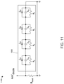
- FIG. 10 is a schematic diagram of one row (or column) of a representative photodetector array 1000 according to one or more embodiments.
- the photodetector array 1000 can be the same as vertical array 830 and/or horizontal array 840 .
- the photodetector array 1000 includes a plurality of photodetectors 1010 that are electrically coupled in series with each other.
- a bias voltage V bias is applied across the photodetectors 1010 .
- a photocurrent is generated when one or more of the photodetectors 1010 detects a photon.
- An optional shunt resistor 1020 is electrically coupled in parallel to each photodetector 1010 to ensure that the bias voltage across each photodetector 1010 is substantially uniform (e.g., within about 10% or less of each other (e.g., in PIN or PN diodes), within about 1% or less of each other, or within about 0.1% of each other (e.g., in avalanche gain devices)) since the gain of each photodetector 1010 is dependent on the bias voltage.
- FIG. 11 is a circuit diagram 1100 of the equivalent circuit formed by representative photodetector array 1000 .
- the circuit diagram 1100 illustrates that each photodetector has a capacitance C D and a photocurrent I DN where N is the photodetector number (e.g., N is an integer of 1 to 4 in FIG. 4 ).
- the bias voltage is N times the bias voltage V diode of a given photodetector since N photodetectors are electrically coupled in series. Since there are 4 photodetectors in series in the photodetector array 1000 , the bias voltage is 4 ⁇ V diode .
- the photocurrent I DN is zero until a photodetector (e.g., photodetector 2 ) detects a photon at which point photocurrent I DN (e.g., I D2 ) flows through that photodetector, for example as illustrated in FIG. 12 . Since the photodetectors are connected in series, the current I D2 must also flow equally through all the other elements in the series connection. As can be seen in FIGS. 11 and 12 , the identity of the photodetector that detected the photon(s) cannot be determined based on the current output by the photodetector array 1000 . For example, the output current would appear the same regardless of which photodetector 1 - 4 detected the photon(s) when the photodetectors and the number of detected photos are otherwise the same.
- the photodetectors 1010 do not include a common connection (e.g., to ground) that often limits the scalability of photodetector arrays.
- the photodetector array 1000 has high temporal resolution (e.g., as simulated by the rise and fall times of the photodetector array 1000 in response to the detection of a single photon). For example, a simulation of the response of (a) a single SiPM, (b) 4 SiPMs in series and (c) 4 SiPMs in parallel yielded the following results (each SiPM was 3 mm ⁇ 3 mm in size):
- the fall time decreased when the SiPMs were electrically coupled in series and increased when they were electrically coupled in parallel.
- the effective capacitance of the SiPM array decreases in direct proportion to the number of SiPMs in the series connection.
- the effect is that the voltage amplitude and signal rise time remain largely unchanged, while the signal fall time is reduced by a corresponding factor (e.g., by approximately 25% compared to a single SiPM).
- the result is that timing performance is almost independent of the number of SiPMs connected in series. Furthermore, there is no significant delay for signal propagation across the array of SiPMs.
- the effective capacitance of the SiPM array increases in direct proportion to the number of SiPMs in the parallel connection.
- the effect is an increase in the fall time in proportion to the effective capacitance (e.g., an increase of over 4 ⁇ compared to a single SiPM), as well as a decrease in signal amplitude (e.g., the amplitude decreases by 4 ⁇ compared to a single SiPM).
- the electrical noise component of the timing jitter scales in in proportion to the number of SiPMs connected in parallel.
- Table 1 provides simulation data for different configurations of SiPMs, the simulation data would be the same as or similar to that for other types of photodetectors. For example, the simulation data would be the same as or similar to that of PIN photodiodes, PN diodes, integrated avalanche photodiode arrays, photoconductors, and APDs for the configurations in Table 1.
- the electrical noise component of the timing jitter is determined according to the following equation:
- ⁇ t electrical noise
- ⁇ v electrical noise
- dv/dt the slope of the pulse rising edge
- dv/dt is proportional to Vmax/risetime, where Vmax is the peak value of the voltage response, and rise time is leading edge rise time of the pulsed response.
- Table 1 also indicates that for the series-connected photodetector arrays, the integrated current scales as 1/N, where N is the number of photodetectors connected in series, while for the parallel-connected photodetector arrays, the voltage scales as 1/N, where N is the number of photodetectors connected in parallel.
- the loss in current may not be a significant concern, particularly for applications where detection is based on voltage amplitude.
- the voltage amplitude is relatively independent of the number of photodetectors connected in series.
- the signal amplitude is reduced since the signal starts decaying before it can reach the maximum amplitude.
- the voltage amplitude of the array is reduced by about a factor of 2 ⁇ (6 dB) compared to the voltage amplitude of a single element.
- Table 2 summarizes estimated properties of various photodetector configurations.
- FIG. 13 is a schematic electrical diagram of a representative photodetector array 1300 according to an alternative embodiment.
- the photodetector array 1300 can be the same as vertical array 830 and/or horizontal array 840 .
- the photodetector array 1300 includes a plurality of photodetectors 1310 that are electrically coupled in series with each other.
- the bias voltage V SIPM is electrically coupled in parallel to each photodetector 1310 , which allows a lower bias voltage (V SIPM ) to be used in photodetector array 1300 than in photodetector array 1000 , which requires N ⁇ V SIPM due to the series connection of the bias voltage to each photodetector 1010 .
- this configuration may relax the accuracy tolerance on the resistors R, provided the voltage drop across each R is relatively small. For example, 10% accuracy resistors R can be used provided the shunt resistance of the photodetectors Rs is larger than about
- VA and HA readouts lines 1410 , 1420 can be used in photodetector grid 810 of device 1400 , as illustrated in FIG. 14 .
- the VA readout line 1410 is electrically coupled to each vertical array 830 and the HA readout line 1420 is electrically coupled to each horizontal array 820 .
- a passive circuit element 1430 is electrically coupled between terminations 1440 of adjacent vertical arrays 830 , between the termination 1440 of the first vertical array 830 A and the X low output, and between the termination 1440 of the last vertical array 830 H and the X hi output.
- a passive circuit element 1430 is electrically coupled between terminations 1440 of adjacent horizontal arrays 820 , between the termination 1440 of the first horizontal array 820 A and the Y hi output, and between the termination 1440 of the last horizontal array 820 H and the Y low output.
- An RF amplifier can be electrically coupled between the outermost or last passive circuit element 1430 and each output (Y hi , Y low , X hi , X low ).
- an RF amplifier can be electrically coupled between (a) the passive circuit element 1430 that is electrically coupled between the termination 1440 of the last horizontal array 820 H and the Y low output and (b) the Y low output.
- a passive circuit element 830 is electrically coupled between terminations 1440 of adjacent horizontal arrays 820 , between the termination 1440 of the first horizontal array 820 A and the Y low output, and between the termination 1440 of the last horizontal array 820 H and the Y hi output.
- the passive circuit elements 1430 can be or comprise a resistor, a capacitor, and/or an inductor. Common approaches use either (a) a resistor or (b) a resistor and capacitor that are electrically coupled in parallel to each other.
- the passive circuit elements 1430 cause the current flowing out of the horizontal arrays 820 (or vertical arrays 830 ) to the readout outputs Y low and Y hi (or X low and X hi ) to split in proportion to the effective impedance to the readout outputs.
- the splitting ratio varies based on the location of the detecting photodetector array 820 , 830 with respect to the corresponding readout line 1410 , 1420 . For example, current flowing out of the first horizontal array 820 A passes through 1 passive circuit element 1430 to reach the Y hi output but it flows through 8 passive circuit elements 1430 to reach the Y low output.
- the relative current flowing out of outputs Y low and Y hi can be used to determine the vertical (“y”) position of the horizontal array 820 that detected the photon(s) and that generated the photocurrent.
- the relative current flowing out of outputs X low and X hi can be used to determine the horizontal (“x”) position of the vertical array 830 that detected the photon(s) and that generated the photocurrent.
- the x and y positions can be determined as:
- X position I ⁇ ( X hi ) - I ⁇ ( X low ) I ⁇ ( X hi ) + I ⁇ ( X low ) ( 4 )
- Y position I ⁇ ( Y hi ) - I ⁇ ( Y low ) I ⁇ ( X hi ) + I ⁇ ( X low ) ( 5 )
- I(X hi ) and I(X low ) are the current flowing through the X hi and X low outputs, respectively
- I(Y hi ) and I(Y low ) are the current flowing through the Y hi and Y low outputs, respectively.
- the total current (or charge) collected by the photodetector grid 810 can be collected at common output 1450 which includes an optional amplifier 1460 (e.g., an RF amplifier).
- an optional amplifier 1460 e.g., an RF amplifier
- the passive circuit elements 1430 can include or can be an inductor.
- the inductor along with the series-connected photodetector array form a lumped-element transmission line with an effective impedance
- Z o L C and an effective delay of ⁇ square root over (LC) ⁇ per element.
- the effective impedance to Y hi and Y low is equal, so the current splits evenly upwards and downwards.
- the position sensitivity is encoded in the relative arrival times of the signals at Y hi and Y low . If both signals arrive at the same time, then the signal is in the center of the array, and if the signal arrives at Y hi before Y low , the signal is closer to Y hi (or vice versa). The amount of delay between Y hi and Y low can be used to refine the position estimation.
- FIG. 15 is a simplified schematic diagram of a photodetector grid 1510 to illustrate the detection of a photon beam 1500 .
- Photodetector grid 1510 is a simplified version of photodetector grid 810 of FIG. 14 and does not include the common output 1450 for clarity purposes only.
- photodetector grid 1510 is a 6 ⁇ 6 photodetector array photodetectors while photodetector grid 810 of FIG. 14 is an 8 ⁇ 8 photodetector array, but this difference is solely to simplify the illustrations.
- the photon beam 1500 is emitted onto photodetectors 1521 , 1522 , 1531 , and 1532 of photodetector array 1510 .
- Photodetectors 1521 , 1532 are HA photodetectors 801
- photodetectors 1522 , 1531 are VA photodetectors 802 .
- Photodetector 1521 is located in horizontal array 1520 A
- photodetector 1522 is located in vertical array 1530 F
- photodetector 1531 is located in vertical array 1530 E
- photodetector 1532 is located in horizontal array 1520 B.
- the output of the HA readout line 1420 indicates (e.g., according to equation (2)) that the “y” position of the centroid of the photon beam 1500 is located between horizontal arrays 1520 A and 1520 B.
- the signal (photocurrent) from horizontal array 1520 A is much greater than the signal (photocurrent) from horizontal array 1520 B because the photon beam 1500 is located more on photodetector 1521 than on photodetector 1532 .
- the signal from horizontal array 1520 A splits with about 5 ⁇ 6 going to Y hi and 1 ⁇ 6 going to Y low .
- Y position corresponds to horizontal array 1520 A.
- the output of the VA readout line 1410 indicates (e.g., according to equation (1)) that the “x” position of the photon beam 1500 is located at vertical arrays 1530 E and 1530 F.
- the actual position of the photon beam 1500 can then be determined based on which horizontal and vertical arrays 1520 , 1530 output current.
- horizontal arrays 1520 A and 1520 B output current
- vertical arrays 1530 E and 1530 F output current.
- These horizontal and vertical arrays intersect at photodetectors 1521 , 1522 , 1531 , and 1532 , which correspond to the detected position of the photon beam 1500 .
- the ratio of photocurrent detected at X hi and X low corresponds to the position of the photon beam 1500 with respect to vertical arrays 1530 E and 1530 F.
- the dimensions of the HA and VA photodetectors 801 , 802 can be selected so that at least a portion of the photon beam 1500 is directed to at least 4 photodetectors (e.g., 2 HA photodetectors 801 and 2 VA photodetectors 802 ) based on the dimensions (or expected dimensions) of the photon beam 1500 .
- the HA and VA photodetectors 801 , 802 can have a width and a length of about 3 mm when the photon beam 1500 has a diameter of at least about 3.1 mm.
- FIG. 16 is a schematic diagram of a position-sensitive photodetector device 1600 according to an alternative embodiment.
- the device 1600 includes a plurality of photodetectors arranged as a photodetector grid 1610 .
- the photodetector grid 1610 includes horizontal arrays 1620 of HA photodetectors 801 and vertical arrays 1630 of VA photodetectors 802 .
- the HA photodetectors 801 are electrically coupled in series in the same manner as they are in each horizontal array 820 .
- the VA photodetectors 802 are electrically coupled in series in the same manner as they are in each vertical array 830 .
- the HA and VA photodetectors 801 , 802 are arranged in rows 1640 and columns 1650 to form the photodetector grid 1610 .
- Rows 1640 B, 1640 D (e.g., a first group of rows) include all of the HA photodetectors 801 in a corresponding horizontal array 1620 .
- Rows 1640 B, 1640 D do not include any VA photodetectors 802 .
- Rows 1640 A, 1640 C (e.g., a second group of rows) include VA photodetector 802 from different vertical arrays 1630 , respectively.
- row 1640 A includes one VA photodetector 802 from each of four different vertical arrays 1630 .
- Each column 1650 includes the VA photodetectors 802 from a corresponding vertical array 1630 and HA photodetectors 801 from different horizontal arrays 1620 .
- column 1650 A includes the VA photodetectors 802 from vertical array 1630 A and one HA photodetector 801 from each of horizontal arrays 1620 A, 1620 B.
- the photodetector grid 1610 has a “horizontally-striped” configuration.
- the photodetector grid 1610 has an alternating sequence of HA and VA photodetectors 801 , 802 in each column 1650 while each row 1640 has the same type of photodetector.
- row 1640 A only includes VA photodetectors 801
- row 1640 B only includes HA photodetectors 802 .
- the photodetector grid 1610 can have a “vertically-striped” configuration where each column 1650 has the same type of photodetector and each row 1640 has an alternating sequence of HA and VA photodetectors 801 , 802 .
- the photodetector grid 1610 includes N/2 rows of HA photodetectors 801 , N/2 rows of VA photodetectors 802 , and N columns, each column having N/2 HA photodetectors 801 and N/2 VA photodetectors. Since horizontal position is determined using the HA photodetectors 801 and vertical position is determined using the VA photodetectors 802 , good position resolution requires that the beam spot size include at least two different HA rows. This is readily achieved by spreading out the beam using optics. The minimum spot size is larger in the horizontally-striped configuration than that for the checkerboard configuration, and generally the spot size should be larger than the area of 9 photodetector elements.
- the HA and VA photodetectors 801 , 802 can have a width and a length of about 3 mm when the photon beam (e.g., photon beam 1500 ) has a diameter of at least about 6.1 mm.
- the position-sensitive photodetector device 1600 includes VA readout line 1410 (e.g., with X hi and X low outputs) and an HA readout line 1420 (e.g., with Y hi and Y low readouts) with passive circuit elements 1430 electrically coupled between each termination 1440 of adjacent horizontal arrays 1620 or vertical arrays 1630 , and between the outermost horizontal or vertical array 1620 , 1630 and the corresponding output (Y hi , Y low , X hi , X low ), similar to the configuration of position-sensitive photodetector device 1400 .
- the position of the photon beam can be determined using the position-sensitive photodetector device 1600 (horizontally-striped configuration) in the same manner as using photodetector grid 1510 (checkerboard configuration).
- FIG. 17 is a block diagram of a position-sensitive photodetection system 1700 according to one or more embodiments.
- the system 1700 includes a photodetector apparatus 1710 that is electrically coupled to a computer 1720 .
- the photodetector apparatus 1710 can be the same as device 80 , 1400 , or 1600 and can comprise any of the photodetector grids described herein (e.g., 810 , 1510 , 1610 ).
- the photodetector apparatus 1710 includes at least 4 outputs, which correspond to the X hi , X low , Y hi , and Y low readouts (e.g., in VA and HA readout lines 1410 , 1420 ).
- the total signal (e.g., common output 1450 ) can be detected using a summing terminal 1450 or by adding the X hi , X low , Y hi , and Y low readouts.
- it is useful to use the common output to determine the arrival time of a pulsed photon beam since the common output will have the largest signal amplitude and therefore the lowest timing jitter according to Equation 3.
- the photodetector apparatus 1710 can include a separate output for the common output.
- it is useful to use the common output to determine the arrival time of a pulsed photon beam since the common output will have the largest signal amplitude and therefore the lowest timing jitter according to Equation 3.
- the computer 1710 receives data signals (e.g., analog or digital signals) that correspond to the electrical properties (e.g., current and voltage as a function of time) of the “x” and “y” readouts and, optionally, of the common output. Using the data signals, the computer can calculate the position of incoming photons using equations (4) and (5) and the number of photons detected based on the common output signal. The computer 1720 can use lookup tables to more precisely locate the x- and y-position of incoming photons based on a previous calibration or calculation using the equivalent circuit models.
- data signals e.g., analog or digital signals
- the computer can calculate the position of incoming photons using equations (4) and (5) and the number of photons detected based on the common output signal.
- the computer 1720 can use lookup tables to more precisely locate the x- and y-position of incoming photons based on a previous calibration or calculation using the equivalent circuit models.
- the photodetector grids in the figures are illustrated as square arrays of photodetectors, other photodetector grid array shapes are possible.
- the photodetector grids can be configured as rectangular arrays, circular array, oval arrays, triangular arrays, hexagonal arrays, or other shape arrays.
- the photodetectors are illustrated as square, other photodetector shapes are possible.
- the photodetectors can be rectangular, triangular, hexagonal, round, or other shapes.
- the photodetector grids and corresponding apparatus have been described in terms of columns and rows which generally lay in a plane defined by the Cartesian coordinate system.
- different photodetector arrangements can be used for other coordinate systems.
- the plane in which the photodetectors are arranged can be defined by the polar coordinate system and the photodetectors can be arranged at different radii and angles with respect to a reference location.
Landscapes
- Engineering & Computer Science (AREA)
- Computer Networks & Wireless Communication (AREA)
- Physics & Mathematics (AREA)
- General Physics & Mathematics (AREA)
- Radar, Positioning & Navigation (AREA)
- Remote Sensing (AREA)
- Light Receiving Elements (AREA)
Abstract
Description
where IA, IB, IC, and ID are the photocurrents from photodetectors A, B, C, and D, respectively, as shown in
| TABLE 1 | ||||
| 1 SiPM | 4 SiPMs in series | 4 SiPMs in parallel | ||
| Rise time | <100 ps | <100 ps | <100 ps |
| Fall time | 10.9 ns | 2.7 ns | 60.6 ns |
| Fall time ratio | 1:1 | 1:4 | >4:1 |
| |
100% | >90% | 25% |
| Peak current | 100% | >90% | 100% |
| Integrated current | 100% | 25% | 100 |
| Voltage Bias | |||
| 100% | 400% | 100% | |
| TABLE 2 | ||||
| Capacitance | Electrical | |||
| per readout | Voltage | timing jitter | ||
| circuit | Amplitude | σt(electrical noise) | ||
| Individual SiPM | CSiPM | 1 | 1 |
| Parallel connection | N2 × CSiPM | 1/N2 | N2 |
| N × N SiPMs | |||
| (1 readout circuit) | |||
| Series connection | CSiPM/N2 | 1 | 1 |
| N × N SiPMs | |||
| (1 readout circuit) | |||
| N × N array SiPMs in | N2 × CSiPM/4 | 4/N2 | 4/N2 |
| parallel using | |||
| resistive Anger | |||
| Logic readout | |||
| (4 readout circuits) | |||
| N × N array of SiPMs, | CSiPM | 1 | 1 |
| checkerboard | |||
| configuration using | |||
| resistive Anger | |||
| Logic combination | |||
| at edges | |||
| (4 readout circuits) | |||
| N × N array of SiPMs, | ~CSiPM/N | 1 | 1 |
| checkerboard | |||
| configuration, using | |||
| hybrid Anger Logic | |||
| readout with pole | |||
| zero compensation | |||
In
where I(Xhi) and I(Xlow) are the current flowing through the Xhi and Xlow outputs, respectively, and I(Yhi) and I(Ylow) are the current flowing through the Yhi and Ylow outputs, respectively.
and an effective delay of √{square root over (LC)} per element. In this embodiment, the effective impedance to Yhi and Ylow is equal, so the current splits evenly upwards and downwards. The position sensitivity is encoded in the relative arrival times of the signals at Yhi and Ylow. If both signals arrive at the same time, then the signal is in the center of the array, and if the signal arrives at Yhi before Ylow, the signal is closer to Yhi (or vice versa). The amount of delay between Yhi and Ylow can be used to refine the position estimation.
Y hi=75%×⅚+25%× 4/6=0.79 (about 8/10)
Y low=75%×⅙+25%× 2/6=0.21 (about 2/10)
This means that the signal is about 4% lower than centered in
Claims (19)
Priority Applications (1)
| Application Number | Priority Date | Filing Date | Title |
|---|---|---|---|
| US16/557,149 US11264422B2 (en) | 2019-08-30 | 2019-08-30 | Scalable position-sensitive photodetector device |
Applications Claiming Priority (1)
| Application Number | Priority Date | Filing Date | Title |
|---|---|---|---|
| US16/557,149 US11264422B2 (en) | 2019-08-30 | 2019-08-30 | Scalable position-sensitive photodetector device |
Publications (2)
| Publication Number | Publication Date |
|---|---|
| US20210066382A1 US20210066382A1 (en) | 2021-03-04 |
| US11264422B2 true US11264422B2 (en) | 2022-03-01 |
Family
ID=74681814
Family Applications (1)
| Application Number | Title | Priority Date | Filing Date |
|---|---|---|---|
| US16/557,149 Expired - Fee Related US11264422B2 (en) | 2019-08-30 | 2019-08-30 | Scalable position-sensitive photodetector device |
Country Status (1)
| Country | Link |
|---|---|
| US (1) | US11264422B2 (en) |
Cited By (2)
| Publication number | Priority date | Publication date | Assignee | Title |
|---|---|---|---|---|
| US20210223414A1 (en) * | 2020-01-21 | 2021-07-22 | LightSpin Technologies Inc. | Modular pet detector |
| USRE49174E1 (en) * | 2016-04-15 | 2022-08-16 | Saint-Gobain Ceramics & Plastics, Inc. | Photosensors arranged on a surface of a scintillator |
Citations (9)
| Publication number | Priority date | Publication date | Assignee | Title |
|---|---|---|---|---|
| US20030222200A1 (en) * | 2002-06-04 | 2003-12-04 | David Skurnik | Very high speed photodetector system using a PIN photodiode array for position sensing |
| US7476864B2 (en) | 2003-04-10 | 2009-01-13 | Jose Maria Benlloch Bavciera | Gamma ray detector with interaction depth coding |
| US20110210255A1 (en) | 2010-02-28 | 2011-09-01 | Chang Lyong Kim | multiplexing readout scheme for a gamma ray detector |
| US20120175498A1 (en) * | 2011-01-10 | 2012-07-12 | Alexander Krymski | Image sensors and methods with shared control lines |
| US9076707B2 (en) | 2013-04-19 | 2015-07-07 | Lightspin Technologies, Inc. | Integrated avalanche photodiode arrays |
| US9698181B2 (en) | 2011-08-03 | 2017-07-04 | Oxford University Innovation Limited | Semiconductor detector device |
| US9768211B2 (en) | 2015-05-06 | 2017-09-19 | LightSpin Technologies Inc. | Integrated avalanche photodiode arrays |
| US20180078766A1 (en) * | 2015-04-15 | 2018-03-22 | Pixium Vision | Pixel cell circuit and implant |
| US10529884B2 (en) | 2017-11-09 | 2020-01-07 | LightSpin Technologies Inc. | Virtual negative bevel and methods of isolating adjacent devices |
-
2019
- 2019-08-30 US US16/557,149 patent/US11264422B2/en not_active Expired - Fee Related
Patent Citations (11)
| Publication number | Priority date | Publication date | Assignee | Title |
|---|---|---|---|---|
| US20030222200A1 (en) * | 2002-06-04 | 2003-12-04 | David Skurnik | Very high speed photodetector system using a PIN photodiode array for position sensing |
| US6831263B2 (en) | 2002-06-04 | 2004-12-14 | Intel Corporation | Very high speed photodetector system using a PIN photodiode array for position sensing |
| US6952003B2 (en) | 2002-06-04 | 2005-10-04 | Intel Corporation | Very high speed photodetector system using a PIN photodiode array for position sensing |
| US7476864B2 (en) | 2003-04-10 | 2009-01-13 | Jose Maria Benlloch Bavciera | Gamma ray detector with interaction depth coding |
| US20110210255A1 (en) | 2010-02-28 | 2011-09-01 | Chang Lyong Kim | multiplexing readout scheme for a gamma ray detector |
| US20120175498A1 (en) * | 2011-01-10 | 2012-07-12 | Alexander Krymski | Image sensors and methods with shared control lines |
| US9698181B2 (en) | 2011-08-03 | 2017-07-04 | Oxford University Innovation Limited | Semiconductor detector device |
| US9076707B2 (en) | 2013-04-19 | 2015-07-07 | Lightspin Technologies, Inc. | Integrated avalanche photodiode arrays |
| US20180078766A1 (en) * | 2015-04-15 | 2018-03-22 | Pixium Vision | Pixel cell circuit and implant |
| US9768211B2 (en) | 2015-05-06 | 2017-09-19 | LightSpin Technologies Inc. | Integrated avalanche photodiode arrays |
| US10529884B2 (en) | 2017-11-09 | 2020-01-07 | LightSpin Technologies Inc. | Virtual negative bevel and methods of isolating adjacent devices |
Non-Patent Citations (25)
| Title |
|---|
| (IDS NPL Cite 7) D'Incecco et al. "Development of a Novel Single-Channel 24cm∧2, SiPM-based, Cryogenic Photodetector", IEEE Transactions on Nuclear Science, 2018, p. 591-596, vol. 65 Issue 1, IEEE (Year: 2018). * |
| D. Schaart et al., "A novel, SiPM-array-based, monolithic scintillator detector for PET", Physics in Medicine and Biology, 2009, pp. 3501-3512, vol. 54, Institute of Physics and Engineering in Medicine. |
| G. B. Ko et al., "Development of a Front-end Analog Circuit for Multi-Channel SiPM Readout and Performance Verification for Various PET Detector Designs", Nuclear Instruments and Methods in Physic Research, 2013, p. 38-44, vol. 703, Elsevier. |
| H. Choe et al., "Protoype Time-of-Flight PET Utilizing Capacitive Multiplexing Readout Method", Nuclear Inst. and Methods in Physics Research Section A, Mar. 2019, p. 43-49, vol. 921, Elsevier. |
| H. Park et al., "Hybrid Charge Division Multiplexing Method for Silicon Photomultiplier Based PET Detectors", IOP Science, May 2017, p. 4390-4405, vol. 62 No. 11, Institute of Physics and Engineering in Medicine. |
| High accuracy CMOS position-sensitive photodetector (PSD) A. Mäkynen, T. Ruotsalainen and J. Kostamovaara Electronics Letters Jan. 16, 1997 vol. 33 No. 2 (Year: 1997). * |
| High Performance CMOS position-sensitive photodetectors (PSDs) A. Mäkynen, T. Ruotsalainen, T. Rahkonen, and J. Kostamovaara (Year: 1998). * |
| J. Du et al., "A Simple Capacitive Charge-Division Readout for Position-Sensitive Solid-State Photomultiplier Arrays", NIH Public Access Author Manuscript, Oct. 2013, p. 1-24, vol. 60 Issue 5, IEEE. |
| J. W. Cates et al. , "Evaluation of a clinical TOF-PET detector design that achieves ≤100 ps coincidence time resolution", Phys Med Biol., 2018, p. 1-30, vol. 63 No. 11. |
| J. W. Cates et al., "Highly Multiplexed Signal Readout for a Time-of-Flight Positron Emission Tomography Detector Based on Silicon Photomultipliers", J. Med. Imag., 2017, p. 1-9, vol. 4 No. 1. |
| J. Yeol Yeom et al., "Side readout of long scintillation crystal elements with digital SiPM for TOF-DOI PET", Med. Phys., 2014, pp. 1-9, vol. 41 No. 12, American Association of Physicists in Medicine. |
| K. Leki et al., "Large-Area MPPC with Enhanced VUV Sensitivity for Liquid Xenon Scintillation Detector", Nuclear Instruments and Methods in Physics Research Section A: Accelerators, Spectrometers, Detectors and Associated Equipment, Feb. 2019, p. 1-10, vol. 925, Elsevier. |
| L. H. C. Braga et al., "A Fully Digital 8x16 SiPM Array for PET Applications With Per-Pixel TDCs and Real-Time Energy Output", IEEE Journal of Solid-State Circuits, Jan. 2014, p. 301-314, vol. 49, IEEE. |
| Linear and sensitive CMOS positionsensitive photodetector A. Mäkynen and J. Kostamovaar Electronics Letters Jun. 11, 1998 vol. 34 No. 12 (Year: 1998). * |
| M. Bieniosek, "Electronic Readout Strategies for Silicon Photomultipler-Based Positron Emisson Tomography Detectors", Mar. 2016, p. 1-121, Stanford University. |
| M. D'Incecco et al., "Development of a Novel Single-Channel, 24cm∧2, SiPM-based, Cryogenic Photodetector", IEEE Transactions on Nuclear Science, 2018, p. 591-596,vol. 65 Issue 1, IEEE. |
| M. F. Bieniosek et al., "A Multiplexed TOF and DOI Capable PET Detector Using a Binary Position Sensitive Network", Phys Med Biol, Nov. 2016, p. 1-21, vol. 61 No 21, Institute of Physics and Engineering in Medicine. |
| M. F. Bieniosek et al., "Achieving Fast Timing Performance with Multiplexed SiPMs", Physics in Medicine & Biology, 2016, p. 2879-2892, vol. 61, Institute of Physics and Engineering in Medicine. |
| M. F. Bieniosek et al., "Analog Filtering Methods Improve Leading Edge Timing Performance of Multiplexed SiPMs", Physics in Medicine & Biology, 2016, p. N427-N440, vol. 61, Institute of Physics and Engineering in Medicine. |
| M. Janecek et al., "A High-Speed Multi-Channel Readout for SSPM Arrays", IEEE Transactions on Nuclear Science, 2012, p. 13-18, vol. 59 No. 1, IEEE. |
| P. Peng et al., "Compton PET: a layered structure PET detector with high performance", Physics in Medicine & Biology, 2019, pp. 1-16, vol. 64 No. 10, Institute of Physics and Engineering in Medicine. |
| P. W. Cattaneo et al., "Development of high Precision Timing Counter Based on plastic Scintillator with SiPM Readout", IEEE Transactions on Nuclear Science, Feb. 2014, p. 1-11, IEEE. |
| S. I. Kwon et al., "Signal Encoding Method for a Time-of-Flight PET Detector Using a Silicon Photomultiplier Array", Nuclear Instruments and Methods in Physics Research A, 2014, p. 39-45, vol. 761, Elsevier. |
| S. Moehrs et al., "A Small-Animal PET Design Using SiPMs and Anger Logic with Intrinsic DOI", IEEE Symposium Conference Record Nuclear Science, 2004, p. 3475-3479, vol. 6, IEEE. |
| V. Ilisie et al. , "Building blocks of a multi-layer PET with time sequence photon interaction discrimination and double Compton camera", Nuclear Inst. and Methods in Physics Research, 2018, pp. 1-28, vol. 895, Elsevier. |
Cited By (3)
| Publication number | Priority date | Publication date | Assignee | Title |
|---|---|---|---|---|
| USRE49174E1 (en) * | 2016-04-15 | 2022-08-16 | Saint-Gobain Ceramics & Plastics, Inc. | Photosensors arranged on a surface of a scintillator |
| US20210223414A1 (en) * | 2020-01-21 | 2021-07-22 | LightSpin Technologies Inc. | Modular pet detector |
| US11762108B2 (en) * | 2020-01-21 | 2023-09-19 | LightSpin Technologies Inc. | Modular pet detector comprising a plurality of modular one-dimensional arrays of monolithic detector sub-modules |
Also Published As
| Publication number | Publication date |
|---|---|
| US20210066382A1 (en) | 2021-03-04 |
Similar Documents
| Publication | Publication Date | Title |
|---|---|---|
| US10656288B2 (en) | Digital silicon photomultiplier for TOF-PET | |
| US8476571B2 (en) | SiPM photosensor with early signal digitization | |
| US8319186B2 (en) | Silicon photomultiplier trigger network | |
| US9121766B2 (en) | Multi pixel photo detector array of Geiger mode avalanche photodiodes | |
| US8247780B2 (en) | High density, proportional-mode, APD arrays for individual scintillator readout in PET applications | |
| TWI675219B (en) | Detector | |
| US12523786B2 (en) | Lateral crystal photodiode readouts and switched diode networks for processing nuclear events | |
| US12449554B2 (en) | Scintillator detectors and methods for positron emission tomography | |
| US11264422B2 (en) | Scalable position-sensitive photodetector device | |
| Moses | Photodetectors for nuclear medical imaging | |
| US10605931B2 (en) | SIPM sensor chip | |
| US7495201B2 (en) | Charge multiplexed array of solid-state photosensitive detectors | |
| US20220128721A1 (en) | Sensor chip for detecting light | |
| Acerbi et al. | Reduced-Channels Position-Sensitive 10× 1 SiPM Tile for Scintillator-Bars Readout | |
| CN117308773A (en) | Three-dimensional position sensitive scintillation detector and scintillation imaging detector | |
| CN109997058A (en) | Method for signal processing of photosensors | |
| McClish et al. | Characterization of CMOS position sensitive solid-state photomultipliers | |
| US20220260736A1 (en) | Silicon photomultipliers for positron emission tomography imaging systems | |
| RU162937U1 (en) | SILICON PHOTOMULTIPLICATOR FOR REGISTRATION OF SINGLE PHOTONS | |
| Foudray et al. | Characterization of two thin postion-sensitive avalanche photodiodes on a single flex circuit for use in 3-d positioning pet detectors | |
| Persson et al. | A prototype detector module for combined PET/CT or combined photon counting/standard CT based on SiPM technology |
Legal Events
| Date | Code | Title | Description |
|---|---|---|---|
| FEPP | Fee payment procedure |
Free format text: ENTITY STATUS SET TO UNDISCOUNTED (ORIGINAL EVENT CODE: BIG.); ENTITY STATUS OF PATENT OWNER: SMALL ENTITY |
|
| FEPP | Fee payment procedure |
Free format text: ENTITY STATUS SET TO SMALL (ORIGINAL EVENT CODE: SMAL); ENTITY STATUS OF PATENT OWNER: SMALL ENTITY |
|
| AS | Assignment |
Owner name: LIGHTSPIN TECHNOLOGIES INC., NEW YORK Free format text: ASSIGNMENT OF ASSIGNORS INTEREST;ASSIGNOR:HARMON, ERIC;REEL/FRAME:051315/0720 Effective date: 20191210 |
|
| STPP | Information on status: patent application and granting procedure in general |
Free format text: RESPONSE TO NON-FINAL OFFICE ACTION ENTERED AND FORWARDED TO EXAMINER |
|
| STPP | Information on status: patent application and granting procedure in general |
Free format text: DOCKETED NEW CASE - READY FOR EXAMINATION |
|
| STPP | Information on status: patent application and granting procedure in general |
Free format text: NOTICE OF ALLOWANCE MAILED -- APPLICATION RECEIVED IN OFFICE OF PUBLICATIONS |
|
| STCF | Information on status: patent grant |
Free format text: PATENTED CASE |
|
| FEPP | Fee payment procedure |
Free format text: MAINTENANCE FEE REMINDER MAILED (ORIGINAL EVENT CODE: REM.); ENTITY STATUS OF PATENT OWNER: SMALL ENTITY |
|
| LAPS | Lapse for failure to pay maintenance fees |
Free format text: PATENT EXPIRED FOR FAILURE TO PAY MAINTENANCE FEES (ORIGINAL EVENT CODE: EXP.); ENTITY STATUS OF PATENT OWNER: SMALL ENTITY |
|
| STCH | Information on status: patent discontinuation |
Free format text: PATENT EXPIRED DUE TO NONPAYMENT OF MAINTENANCE FEES UNDER 37 CFR 1.362 |