US11245365B2 - Power amplifier circuit - Google Patents
Power amplifier circuit Download PDFInfo
- Publication number
- US11245365B2 US11245365B2 US16/828,630 US202016828630A US11245365B2 US 11245365 B2 US11245365 B2 US 11245365B2 US 202016828630 A US202016828630 A US 202016828630A US 11245365 B2 US11245365 B2 US 11245365B2
- Authority
- US
- United States
- Prior art keywords
- transistor
- collector
- impedance
- power amplifier
- line
- Prior art date
- Legal status (The legal status is an assumption and is not a legal conclusion. Google has not performed a legal analysis and makes no representation as to the accuracy of the status listed.)
- Active
Links
Images


Classifications
-
- H—ELECTRICITY
- H03—ELECTRONIC CIRCUITRY
- H03F—AMPLIFIERS
- H03F1/00—Details of amplifiers with only discharge tubes, only semiconductor devices or only unspecified devices as amplifying elements
- H03F1/02—Modifications of amplifiers to raise the efficiency, e.g. gliding Class A stages, use of an auxiliary oscillation
- H03F1/0205—Modifications of amplifiers to raise the efficiency, e.g. gliding Class A stages, use of an auxiliary oscillation in transistor amplifiers
-
- H—ELECTRICITY
- H03—ELECTRONIC CIRCUITRY
- H03F—AMPLIFIERS
- H03F3/00—Amplifiers with only discharge tubes or only semiconductor devices as amplifying elements
- H03F3/20—Power amplifiers, e.g. Class B amplifiers, Class C amplifiers
- H03F3/21—Power amplifiers, e.g. Class B amplifiers, Class C amplifiers with semiconductor devices only
-
- H—ELECTRICITY
- H03—ELECTRONIC CIRCUITRY
- H03F—AMPLIFIERS
- H03F1/00—Details of amplifiers with only discharge tubes, only semiconductor devices or only unspecified devices as amplifying elements
- H03F1/02—Modifications of amplifiers to raise the efficiency, e.g. gliding Class A stages, use of an auxiliary oscillation
- H03F1/0205—Modifications of amplifiers to raise the efficiency, e.g. gliding Class A stages, use of an auxiliary oscillation in transistor amplifiers
- H03F1/0211—Modifications of amplifiers to raise the efficiency, e.g. gliding Class A stages, use of an auxiliary oscillation in transistor amplifiers with control of the supply voltage or current
- H03F1/0216—Continuous control
- H03F1/0222—Continuous control by using a signal derived from the input signal
-
- H—ELECTRICITY
- H03—ELECTRONIC CIRCUITRY
- H03F—AMPLIFIERS
- H03F1/00—Details of amplifiers with only discharge tubes, only semiconductor devices or only unspecified devices as amplifying elements
- H03F1/02—Modifications of amplifiers to raise the efficiency, e.g. gliding Class A stages, use of an auxiliary oscillation
- H03F1/0205—Modifications of amplifiers to raise the efficiency, e.g. gliding Class A stages, use of an auxiliary oscillation in transistor amplifiers
- H03F1/0211—Modifications of amplifiers to raise the efficiency, e.g. gliding Class A stages, use of an auxiliary oscillation in transistor amplifiers with control of the supply voltage or current
- H03F1/0216—Continuous control
- H03F1/0233—Continuous control by using a signal derived from the output signal, e.g. bootstrapping the voltage supply
-
- H—ELECTRICITY
- H03—ELECTRONIC CIRCUITRY
- H03F—AMPLIFIERS
- H03F1/00—Details of amplifiers with only discharge tubes, only semiconductor devices or only unspecified devices as amplifying elements
- H03F1/30—Modifications of amplifiers to reduce influence of variations of temperature or supply voltage or other physical parameters
- H03F1/302—Modifications of amplifiers to reduce influence of variations of temperature or supply voltage or other physical parameters in bipolar transistor amplifiers
-
- H—ELECTRICITY
- H03—ELECTRONIC CIRCUITRY
- H03F—AMPLIFIERS
- H03F1/00—Details of amplifiers with only discharge tubes, only semiconductor devices or only unspecified devices as amplifying elements
- H03F1/56—Modifications of input or output impedances, not otherwise provided for
- H03F1/565—Modifications of input or output impedances, not otherwise provided for using inductive elements
-
- H—ELECTRICITY
- H03—ELECTRONIC CIRCUITRY
- H03F—AMPLIFIERS
- H03F3/00—Amplifiers with only discharge tubes or only semiconductor devices as amplifying elements
- H03F3/189—High-frequency amplifiers, e.g. radio frequency amplifiers
-
- H—ELECTRICITY
- H03—ELECTRONIC CIRCUITRY
- H03F—AMPLIFIERS
- H03F3/00—Amplifiers with only discharge tubes or only semiconductor devices as amplifying elements
- H03F3/189—High-frequency amplifiers, e.g. radio frequency amplifiers
- H03F3/19—High-frequency amplifiers, e.g. radio frequency amplifiers with semiconductor devices only
- H03F3/191—Tuned amplifiers
-
- H—ELECTRICITY
- H03—ELECTRONIC CIRCUITRY
- H03F—AMPLIFIERS
- H03F3/00—Amplifiers with only discharge tubes or only semiconductor devices as amplifying elements
- H03F3/20—Power amplifiers, e.g. Class B amplifiers, Class C amplifiers
- H03F3/21—Power amplifiers, e.g. Class B amplifiers, Class C amplifiers with semiconductor devices only
- H03F3/211—Power amplifiers, e.g. Class B amplifiers, Class C amplifiers with semiconductor devices only using a combination of several amplifiers
-
- H—ELECTRICITY
- H03—ELECTRONIC CIRCUITRY
- H03F—AMPLIFIERS
- H03F3/00—Amplifiers with only discharge tubes or only semiconductor devices as amplifying elements
- H03F3/20—Power amplifiers, e.g. Class B amplifiers, Class C amplifiers
- H03F3/21—Power amplifiers, e.g. Class B amplifiers, Class C amplifiers with semiconductor devices only
- H03F3/213—Power amplifiers, e.g. Class B amplifiers, Class C amplifiers with semiconductor devices only in integrated circuits
-
- H—ELECTRICITY
- H03—ELECTRONIC CIRCUITRY
- H03F—AMPLIFIERS
- H03F3/00—Amplifiers with only discharge tubes or only semiconductor devices as amplifying elements
- H03F3/34—DC amplifiers in which all stages are DC-coupled
- H03F3/343—DC amplifiers in which all stages are DC-coupled with semiconductor devices only
- H03F3/3432—DC amplifiers in which all stages are DC-coupled with semiconductor devices only with bipolar transistors
-
- H—ELECTRICITY
- H03—ELECTRONIC CIRCUITRY
- H03F—AMPLIFIERS
- H03F2200/00—Indexing scheme relating to amplifiers
- H03F2200/144—Indexing scheme relating to amplifiers the feedback circuit of the amplifier stage comprising a passive resistor and passive capacitor
-
- H—ELECTRICITY
- H03—ELECTRONIC CIRCUITRY
- H03F—AMPLIFIERS
- H03F2200/00—Indexing scheme relating to amplifiers
- H03F2200/361—Transistor with multiple collectors
-
- H—ELECTRICITY
- H03—ELECTRONIC CIRCUITRY
- H03F—AMPLIFIERS
- H03F2200/00—Indexing scheme relating to amplifiers
- H03F2200/363—Transistor with multiple emitters
-
- H—ELECTRICITY
- H03—ELECTRONIC CIRCUITRY
- H03F—AMPLIFIERS
- H03F2200/00—Indexing scheme relating to amplifiers
- H03F2200/451—Indexing scheme relating to amplifiers the amplifier being a radio frequency amplifier
-
- H—ELECTRICITY
- H03—ELECTRONIC CIRCUITRY
- H03F—AMPLIFIERS
- H03F2200/00—Indexing scheme relating to amplifiers
- H03F2200/555—A voltage generating circuit being realised for biasing different circuit elements
Definitions
- the present disclosure relates to a power amplifier circuit.
- output power can be increased by increasing a power supply voltage.
- a booster circuit is required to increase the power supply voltage. It is therefore desirable to increase output power without necessarily increasing a power supply voltage.
- Japanese Unexamined Patent Application Publication No. 2018-85689 describes a power amplifier circuit that increases the output power without necessarily increasing the power supply voltage.
- a decrease in output impedance provides the merit of increasing output power and the demerit of decreasing power-added efficiency.
- An increase in output impedance provides the merit of increasing power-added efficiency and the demerit of decreasing output power.
- output impedance is an important factor.
- the output impedance provides an optimal trade-off between output power and power-added efficiency.
- the present disclosure achieves a desired trade-off between output power and power-added efficiency.
- a power amplifier circuit includes a first bias circuit that outputs a first bias current or voltage; a second bias circuit that outputs a second bias current or voltage; a first transistor having an emitter, a base, and a collector, wherein the emitter is electrically connected to a reference potential, the first bias current or voltage is input to the base via a first resistor, a radio-frequency input signal is input to the base via a first capacitor, and the collector is electrically connected to a first power supply potential via a first inductor; a capacitor having a first end and a second end, the first end being electrically connected to the collector of the first transistor; and a second transistor having an emitter, a base, and a collector, wherein the emitter is electrically connected to the second end of the capacitor, the emitter is electrically connected to the reference potential via a second inductor, the second bias current or voltage is input to the base via a second resistor, the base is electrically connected to the reference potential via a second capacitor
- the second bias circuit includes a third transistor having a collector, a base, and an emitter, wherein the collector is electrically connected to a second power supply potential, a third bias current or voltage is input to the base, and the second bias current or voltage is output from the emitter.
- a power amplifier circuit includes a first bias circuit that outputs a first bias current or voltage; a second bias circuit that outputs a second bias current or voltage; a first transistor having an emitter, a base, and a collector, wherein the emitter is electrically connected to a reference potential, the first bias current or voltage is input to the base via a first resistor, a radio-frequency input signal is input to the base via a first capacitor, and the collector is electrically connected to a first power supply potential via a first inductor; a capacitor having a first end and a second end, the first end being electrically connected to the collector of the first transistor; and a second transistor having an emitter, a base, and a collector, wherein the emitter is electrically connected to the second end of the capacitor, the emitter is electrically connected to the reference potential via a second inductor, the second bias current or voltage is input to the base via a second resistor, the base is electrically connected to the reference potential via a second capacitor
- FIG. 1 illustrates a circuit configuration of a power amplifier circuit according to a first embodiment
- FIG. 2 illustrates circuit simulation results of the power amplifier circuit according to the first embodiment
- FIG. 3 illustrates circuit simulation results of the power amplifier circuit according to the first embodiment
- FIG. 4 illustrates circuit simulation results of the power amplifier circuit according to the first embodiment
- FIG. 5 illustrates circuit simulation results of the power amplifier circuit according to the first embodiment
- FIG. 6 illustrates circuit simulation results of the power amplifier circuit according to the first embodiment
- FIG. 7 illustrates circuit simulation results of the power amplifier circuit according to the first embodiment
- FIG. 8 illustrates circuit simulation results of the power amplifier circuit according to the first embodiment
- FIG. 9 illustrates circuit simulation results of the power amplifier circuit according to the first embodiment
- FIG. 10 illustrates circuit simulation results of the power amplifier circuit according to the first embodiment
- FIG. 11 illustrates circuit simulation results of the power amplifier circuit according to the first embodiment
- FIG. 12 illustrates circuit simulation results of the power amplifier circuit according to the first embodiment
- FIG. 13 illustrates circuit simulation results of the power amplifier circuit according to the first embodiment
- FIG. 14 illustrates circuit simulation results of the power amplifier circuit according to the first embodiment
- FIG. 15 illustrates circuit simulation results of the power amplifier circuit according to the first embodiment
- FIG. 16 illustrates circuit simulation results of the power amplifier circuit according to the first embodiment
- FIG. 17 illustrates circuit simulation results of a power amplifier circuit according to a second embodiment
- FIG. 18 illustrates circuit simulation results of the power amplifier circuit according to the second embodiment
- FIG. 19 illustrates circuit simulation results of the power amplifier circuit according to the second embodiment
- FIG. 20 illustrates circuit simulation results of the power amplifier circuit according to the second embodiment
- FIG. 21 illustrates circuit simulation results of the power amplifier circuit according to the second embodiment
- FIG. 22 illustrates circuit simulation results of the power amplifier circuit according to the second embodiment
- FIG. 23 illustrates circuit simulation results of a power amplifier circuit according to a third embodiment
- FIG. 24 illustrates circuit simulation results of the power amplifier circuit according to the third embodiment
- FIG. 25 illustrates circuit simulation results of the power amplifier circuit according to the third embodiment
- FIG. 26 illustrates circuit simulation results of the power amplifier circuit according to the third embodiment
- FIG. 27 illustrates circuit simulation results of the power amplifier circuit according to the third embodiment
- FIG. 28 illustrates circuit simulation results of the power amplifier circuit according to the third embodiment
- FIG. 29 illustrates a first example circuit configuration of a bias circuit according to a fifth embodiment
- FIG. 30 illustrates circuit simulation results of the first example circuit configuration according to the fifth embodiment
- FIG. 31 illustrates circuit simulation results of the first example circuit configuration according to the fifth embodiment
- FIG. 32 illustrates circuit simulation results of the first example circuit configuration according to the fifth embodiment
- FIG. 33 illustrates a second example circuit configuration of the bias circuit according to the fifth embodiment
- FIG. 34 illustrates circuit simulation results of the second example circuit configuration according to the fifth embodiment
- FIG. 35 illustrates circuit simulation results of the second example circuit configuration according to the fifth embodiment
- FIG. 36 illustrates circuit simulation results of the second example circuit configuration according to the fifth embodiment
- FIG. 37 illustrates circuit simulation results of the second example circuit configuration according to the fifth embodiment
- FIG. 38 illustrates circuit simulation results of the second example circuit configuration according to the fifth embodiment
- FIG. 39 illustrates circuit simulation results of the second example circuit configuration according to the fifth embodiment
- FIG. 40 illustrates circuit simulation results of the second example circuit configuration according to the fifth embodiment
- FIG. 41 illustrates a third example circuit configuration of the bias circuit according to the fifth embodiment
- FIG. 42 illustrates circuit simulation results of the third example circuit configuration according to the fifth embodiment
- FIG. 43 illustrates circuit simulation results of the third example circuit configuration according to the fifth embodiment
- FIG. 44 illustrates circuit simulation results of the third example circuit configuration according to the fifth embodiment
- FIG. 45 illustrates a fourth example circuit configuration of the bias circuit according to the fifth embodiment
- FIG. 46 illustrates circuit simulation results of the fourth example circuit configuration according to the fifth embodiment
- FIG. 47 illustrates circuit simulation results of the fourth example circuit configuration according to the fifth embodiment
- FIG. 48 illustrates circuit simulation results of the fourth example circuit configuration according to the fifth embodiment
- FIG. 49 illustrates a fifth example circuit configuration of the bias circuit according to the fifth embodiment
- FIG. 50 illustrates circuit simulation results of the fifth example circuit configuration according to the fifth embodiment
- FIG. 51 illustrates circuit simulation results of the fifth example circuit configuration according to the fifth embodiment
- FIG. 52 illustrates circuit simulation results of the fifth example circuit configuration according to the fifth embodiment
- FIG. 53 illustrates circuit simulation results of a power amplifier circuit according to a sixth embodiment
- FIG. 54 illustrates circuit simulation results of the power amplifier circuit according to the sixth embodiment
- FIG. 55 illustrates circuit simulation results of the power amplifier circuit according to the sixth embodiment
- FIG. 56 illustrates circuit simulation results of the power amplifier circuit according to the sixth embodiment
- FIG. 57 illustrates circuit simulation results of the power amplifier circuit according to the sixth embodiment
- FIG. 58 illustrates circuit simulation results of the power amplifier circuit according to the sixth embodiment
- FIG. 60 illustrates circuit simulation results of the power amplifier circuit according to the sixth embodiment.
- FIG. 61 illustrates circuit simulation results of the power amplifier circuit according to the sixth embodiment.
- FIG. 1 illustrates a circuit configuration of a power amplifier circuit 1 according to a first embodiment.
- the power amplifier circuit 1 includes a power amplifier 2 , a first bias circuit 3 , a second bias circuit 4 , a first inductor L 1 , a second inductor L 2 , and a third inductor L 3 .
- the power amplifier circuit 1 is mounted in, for example, a mobile communication device such as a mobile phone device to amplify a radio-frequency (RF) input signal Pin and output an RF output signal Pout.
- RF radio-frequency
- the RF input signal Pin and the RF output signal Pout have frequencies in the range from about several hundreds of megahertz (MHz) to about several tens of gigahertz (GHz) for illustrative purposes, and the present disclosure is not limited thereto.
- the power amplifier 2 may be formed on a semiconductor chip (or die), although the present disclosure is not limited thereto.
- the first inductor L 1 , the second inductor L 2 , and the third inductor L 3 may be formed on a substrate having the semiconductor chip mounted thereon, although the present disclosure is not limited thereto.
- the power amplifier 2 includes a first power amplifier 10 , a second power amplifier 20 , and a capacitor C 12 .
- the capacitor C 12 is electrically connected between the first power amplifier 10 and the second power amplifier 20 .
- the capacitor C 12 blocks direct current (DC) while passing alternating current (AC). That is, the capacitor C 12 is a DC-cut capacitor. Specifically, the capacitor C 12 isolates (blocks) the first power amplifier 10 and the second power amplifier 20 from each other for DC and couples (connects) the first power amplifier 10 and the second power amplifier 20 to each other for AC.
- the first power amplifier 10 amplifies the RF input signal Pin and outputs an amplified RF signal Pm to the capacitor C 12 .
- the capacitor C 12 passes the RF signal Pm.
- the second power amplifier 20 amplifies the RF signal Pm that is passed through the capacitor C 12 and outputs the amplified RF output signal Pout.
- the first power amplifier 10 includes M cells CEL 1 1 , CEL 1 2 , . . . , and CEL 1 M that are connected in parallel with each other, where M is a natural number.
- the cells CEL 1 1 , CEL 1 2 , . . . , and CEL 1 M include transistors Q 1 1 , Q 1 2 , . . . , and Q 1 M , respectively.
- the cells CEL 1 1 , CEL 1 2 , . . . , and CEL 1 M include capacitors Cbb 1 1 , Cbb 1 2 , . . . , and Cbb 1 M , respectively.
- CEL 1 M include resistors Rbb 1 1 , Rbb 1 2 , . . . , and Rbb 1 M , respectively.
- the term “cell”, as used herein, is defined as having a configuration in which a transistor, a capacitor, and a resistor are connected to each other.
- each transistor is a heterojunction bipolar transistor (HBT) for illustrative purposes, and the present disclosure is not limited thereto.
- HBT heterojunction bipolar transistor
- the bases of the transistors Q 1 1 , Q 1 2 , . . . , and Q 1 M are electrically connected to first ends of the resistors Rbb 1 1 , Rbb 1 2 , . . . , and Rbb 1 M , respectively. Second ends of the resistors Rbb 1 1 , Rbb 1 2 , . . . , and Rbb 1 M are electrically connected to a terminal T 3 . A bias current or bias voltage is input to the terminal T 3 from the first bias circuit 3 .
- the bias current or voltage input from the first bias circuit 3 to the terminal T 3 corresponds to a “first bias current or voltage” of the present disclosure.
- the collectors of the transistors Q 1 1 , Q 1 2 , . . . , and Q 1 M are electrically connected to a terminal T 4 .
- a first end of the first inductor L 1 is electrically connected to the terminal T 4 .
- a second end of the first inductor L 1 is electrically connected to a power supply potential Vcc.
- the first inductor L 1 is a choke inductor that passes DC while blocking AC to prevent coupling of RF signals to a power supply circuit.
- the power supply potential Vcc corresponds to a “first power supply potential” of the present disclosure.
- the power supply potential Vcc may be an envelope tracking (ET) power supply or a normal DC power supply.
- the collectors of the transistors Q 1 1 , Q 1 2 , . . . , and Q 1 M are electrically connected to a first end of the capacitor C 12 .
- the cells CEL 1 1 , CEL 1 2 , . . . , and CEL 1 M are sometimes referred to collectively as a “cell CEL 1 ”.
- the transistors Q 1 1 , Q 1 2 , . . . , and Q 1 M are sometimes referred to collectively as a “transistor Q 1 ”.
- the capacitors Cbb 1 1 , Cbb 1 2 , . . . , and Cbb 1 M are sometimes referred to collectively as a “capacitor Cbb 1 ”.
- the resistors Rbb 1 1 , Rbb 1 2 , . . . , and Rbb 1 M are sometimes referred to collectively as a “resistor Rbb 1 ”.
- the cell CEL 1 corresponds to a “first cell” of the present disclosure.
- the transistor Q 1 corresponds to a “first transistor” of the present disclosure.
- the capacitor Cbb 1 corresponds to a “first capacitor” of the present disclosure.
- the resistor Rbb 1 corresponds to a “first resistor” of the present disclosure.
- the second power amplifier 20 includes N cells CEL 2 1 , CEL 2 2 , . . . , and CEL 2 N that are connected in parallel with each other, where N is a natural number.
- the number N of cells CEL 2 1 , CEL 2 2 , . . . , and CEL 2 N may be the same as or different from the number M of cells CEL 1 1 , CEL 1 2 , . . . , and CEL 1 M .
- the cells CEL 2 1 , CEL 2 2 , . . . , and CEL 2 N include transistors Q 2 1 , Q 2 2 , . . . , and Q 2 N , respectively.
- the cells CEL 2 1 , CEL 2 2 , . . . , and CEL 2 N include capacitors Cbb 2 1 , Cbb 2 2 , . . . , and Cbb 2 N , respectively.
- the cells CEL 2 1 , CEL 2 2 , . . . , and CEL 2 N include resistors Rbb 2 1 , Rbb 2 2 , . . . , and Rbb 2 N , respectively.
- the emitters of the transistors Q 2 1 , Q 2 2 , . . . , and Q 2 N are electrically connected to a second end of the capacitor C 12 .
- the emitters of the transistors Q 2 1 , Q 2 2 , . . . , and Q 2 N are electrically connected to a terminal T 5 .
- a first end of the second inductor L 2 is electrically connected to the terminal T 5 .
- a second end of the second inductor L 2 is electrically connected to the reference potential.
- the second inductor L 2 is a choke inductor that passes DC while blocking AC.
- the bases of the transistors Q 2 1 , Q 2 2 , . . . , and Q 2 N are electrically connected to first ends of the capacitors Cbb 2 1 , Cbb 2 2 , . . . , and Cbb 2 N , respectively.
- Second ends of the capacitors Cbb 2 1 , Cbb 2 2 , . . . , and Cbb 2 N are electrically connected to a terminal T 6 .
- the terminal T 6 is electrically connected to the reference potential.
- the capacitors Cbb 2 1 , Cbb 2 2 , . . . , and Cbb 2 N block DC while passing AC.
- the bases of the transistors Q 2 1 , Q 2 2 , . . . , and Q 2 N are electrically connected to first ends of the resistors Rbb 2 1 , Rbb 2 2 , . . . , and Rbb 2 N , respectively. Second ends of the resistors Rbb 2 1 , Rbb 2 2 , . . . , and Rbb 2 N are electrically connected to a terminal T 7 . A bias current or bias voltage is input to the terminal T 7 from the second bias circuit 4 .
- the bias current or voltage input from the second bias circuit 4 to the terminal T 7 corresponds to a “second bias current or voltage” of the present disclosure.
- the collectors of the transistors Q 2 1 , Q 2 2 , . . . , and Q 2 N are electrically connected to a terminal T 8 .
- a first end of the third inductor L 3 is electrically connected to the terminal T 8 .
- a second end of the third inductor L 3 is electrically connected to the power supply potential Vcc.
- the third inductor L 3 is a choke inductor that passes DC while blocking AC to prevent coupling of RF signals to a power supply circuit.
- a first end of a matching circuit 101 is electrically connected to the terminal T 8 .
- a second end of the matching circuit 101 is electrically connected to a first end of a load circuit 102 .
- the matching circuit 101 is configured using an inductor and a capacitor for illustrative purposes, and the present disclosure is not limited thereto.
- the load circuit 102 is a front-end circuit connected to an antenna for illustrative purposes, and the present disclosure is not limited thereto.
- the cells CEL 2 1 , CEL 2 2 , . . . , and CEL 2 N are sometimes referred to collectively as a “cell CEL 2 ”.
- the transistors Q 2 1 , Q 2 2 , . . . , and Q 2 N are sometimes referred to collectively as a “transistor Q 2 ”.
- the capacitors Cbb 2 1 , Cbb 2 2 , . . . , and Cbb 2 N are sometimes referred to collectively as a “capacitor Cbb 2 ”.
- the resistors Rbb 2 1 , Rbb 2 2 , . . . , and Rbb 2 N are sometimes referred to collectively as a “resistor Rbb 2 ”.
- the cell CEL 2 corresponds to a “second cell” of the present disclosure.
- the transistor Q 2 corresponds to a “second transistor” of the present disclosure.
- the capacitor Cbb 2 corresponds to a “second capacitor” of the present disclosure.
- the resistor Rbb 2 corresponds to a “second resistor” of the present disclosure.
- the power supply potential Vcc is supplied to the collector of the transistor Q 2 via the third inductor L 3 , and the emitter of the transistor Q 2 is grounded via the second inductor L 2 .
- the RF signal Pm is input to the emitter of the transistor Q 2 from the first power amplifier 10 via the capacitor C 12 .
- a bias current or a bias voltage is supplied to the base of the transistor Q 2 from the second bias circuit 4 . Accordingly, the transistor Q 2 amplifies the RF signal Pm and outputs the amplified RF output signal Pout to the load circuit 102 via the matching circuit 101 .
- the first end of the capacitor C 12 is electrically connected to the collector of the transistor Q 1 , and the second end of the capacitor C 12 is electrically connected to the emitter of the transistor Q 2 .
- the capacitor C 12 isolates the transistor Q 1 and the transistor Q 2 from each other for DC and couplies the transistor Q 1 and the transistor Q 2 to each other for AC.
- the transistor Q 1 The emitter of the transistor Q 1 is grounded, and the power supply potential Vcc (here, DC3V) is supplied to the collector of the transistor Q 1 via the first inductor L 1 . Accordingly, the RF signal Pm has an amplitude swing of ⁇ 3 V for AC (hereinafter sometimes referred to as AC ⁇ 3V). That is, the collector potential of the transistor Q 1 varies over a range of 3 V ⁇ 3 V, that is, a range from 0 V to +6 V.
- the emitter of the transistor Q 2 is grounded for DC, resulting in DC0V, and is coupled (connected) to the collector of the transistor Q 1 for AC, resulting in AC ⁇ 3V.
- the emitter voltage of the transistor Q 2 varies over a range of 0 V ⁇ 3 V, that is, a range from ⁇ 3 V to +3 V.
- the collector of the transistor Q 2 is supplied with the power supply potential Vcc for DC, and thus the collector potential of the transistor Q 2 is DC3V.
- the collector potential of the transistor Q 2 is in a range of AC ⁇ 6V including the range over which the emitter voltage of the transistor Q 2 varies.
- the RF output signal Pout has an amplitude swing of AC ⁇ 6V. That is, the collector potential of the transistor Q 2 varies over a range of 3 V ⁇ 6 V, that is, a range from ⁇ 3 V to +9 V.
- the power amplifier 2 has a cascode configuration in which the first power amplifier 10 and the second power amplifier 20 are connected to each other via the capacitor C 12 .
- the power amplifier 2 can increase the amplitude of the RF output signal Pout (for example, 12 V, from ⁇ 3 V to +9 V) to a value that is about twice as large as the amplitude of an output signal of a power amplifier with a single configuration (for example, 6 V, from 0 V to +6 V). That is, the power amplifier 2 can increase the amplitude of the RF output signal Pout without necessarily increasing the power supply potential using a booster circuit.
- the power amplifier 2 can increase the output power, compared to that of a power amplifier with a single configuration, by increasing the amplitude of the RF output signal Pout without necessarily increasing the power supply potential.
- the load impedance R is substantially quadrupled.
- the impedance transformation ratio is a transformation ratio for performing impedance matching for a load circuit. Accordingly, the band-pass loss and the return loss of the matching circuit are reduced, and the power-added efficiency (PAE) improves.
- the load impedance increases with an increase in the amplitude of the RF output signal Pout, resulting in a decrease in the impedance transformation ratio of the matching circuit 101 .
- the power amplifier 2 provides improved power-added efficiency with reduced loss of the RF output signal Pout in the matching circuit 101 , compared to a power amplifier with a single configuration. As described above, the power amplifier 2 can also improve power-added efficiency.
- a decrease in output impedance provides the merit of increasing output power and the demerit of decreasing power-added efficiency.
- An increase in output impedance provides the merit of increasing power-added efficiency and the demerit of decreasing output power.
- output impedance is an important factor.
- the output impedance provides an optimal trade-off between output power and power-added efficiency.
- the output impedance of the first power amplifier 10 (collector impedance of the transistor Q 1 ) and the output impedance of the second power amplifier 20 (collector impedance of the transistor Q 2 ) are important factors. Desirably, the output impedance of the first power amplifier 10 and the output impedance of the second power amplifier 20 can achieve a desired trade-off between the output power and power-added efficiency of the power amplifier 2 .
- the present inventors performed circuit simulation on the power amplifier 2 .
- the following describes results of the circuit simulation. First, description will be given of a case where a collector impedance ZL_Q 2 of the transistor Q 2 has no imaginary part. Later, description will be given of a case where the collector impedance ZL_Q 2 of the transistor Q 2 has an imaginary part.
- the real part of the ratio of the collector impedance ZL_Q 2 of the transistor Q 2 to a collector impedance ZL_Q 1 of the transistor Q 1 is substantially the same when the collector impedance ZL_Q 2 of the transistor Q 2 has an imaginary part and when the collector impedance ZL_Q 2 of the transistor Q 2 has no imaginary part. Accordingly, the present disclosure is not limited to the case where the collector impedance ZL_Q 2 of the transistor Q 2 has no imaginary part. This also applies to the second and subsequent embodiments.
- the circuit simulation was based on the assumption that an impedance Zref of the load circuit 102 was set to 6 ohms ( ⁇ ). Further, the collector impedance ZL_Q 2 of the transistor Q 2 was set to various values (such as 2 ⁇ , 4 ⁇ , 6 ⁇ , 8 ⁇ , and 10 ⁇ ).
- the default value of the frequency of the RF input signal Pin is 3.3 GHz.
- FIGS. 2 to 6 illustrate circuit simulation results of the power amplifier circuit 1 according to the first embodiment.
- FIG. 2 is a Smith chart of the collector impedance ZL_Q 2 of the transistor Q 2 .
- FIG. 3 is a Smith chart of the collector impedance ZL_Q 1 of the transistor Q 1 .
- point 201 is a point at which the collector impedance ZL_Q 2 of the transistor Q 2 is 2 ⁇ .
- Point 202 is a point at which the collector impedance ZL_Q 2 of the transistor Q 2 is 4 ⁇ .
- Point 203 is a point at which the collector impedance ZL_Q 2 of the transistor Q 2 is 6 ⁇ .
- Point 204 is a point at which the collector impedance ZL_Q 2 of the transistor Q 2 is 8 ⁇ .
- Point 205 is a point at which the collector impedance ZL_Q 2 of the transistor Q 2 is 10 ⁇ .
- line 211 represents the locus of the collector impedance ZL_Q 1 of the transistor Q 1 when the collector impedance ZL_Q 2 of the transistor Q 2 was set to 2 ⁇ .
- Line 212 represents the locus of the collector impedance ZL_Q 1 of the transistor Q 1 when the collector impedance ZL_Q 2 of the transistor Q 2 was set to 4 ⁇ .
- Line 213 represents the locus of the collector impedance ZL_Q 1 of the transistor Q 1 when the collector impedance ZL_Q 2 of the transistor Q 2 was set to 6 ⁇ .
- Line 214 represents the locus of the collector impedance ZL_Q 1 of the transistor Q 1 when the collector impedance ZL_Q 2 of the transistor Q 2 was set to 8 ⁇ .
- Line 215 represents the locus of the collector impedance ZL_Q 1 of the transistor Q 1 when the collector impedance ZL_Q 2 of the transistor Q 2 was set to 10 ⁇ .
- the operating state of the transistor Q 1 changes in accordance with the set value of the collector impedance ZL_Q 2 of the transistor Q 2 and the output power of the power amplifier 2 .
- the locus of the collector impedance ZL_Q 1 of the transistor Q 1 is indicated by a line.
- FIG. 4 illustrates a relationship between the signal strength (dBm) of the RF output signal Pout and the gain (dB) of the power amplifier 2 .
- Line 221 represents the locus of the gain of the power amplifier 2 when the collector impedance ZL_Q 2 of the transistor Q 2 was set to 2 ⁇ .
- Line 222 represents the locus of the gain of the power amplifier 2 when the collector impedance ZL_Q 2 of the transistor Q 2 was set to 4 ⁇ .
- Line 223 represents the locus of the gain of the power amplifier 2 when the collector impedance ZL_Q 2 of the transistor Q 2 was set to 6 ⁇ .
- Line 224 represents the locus of the gain of the power amplifier 2 when the collector impedance ZL_Q 2 of the transistor Q 2 was set to 8 ⁇ .
- Line 225 represents the locus of the gain of the power amplifier 2 when the collector impedance ZL_Q 2 of the transistor Q 2 was set to 10 ⁇ .
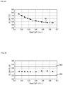
- the collector impedance ZL_Q 2 of the transistor Q 2 is set to about 6 ⁇ ((6 ⁇ ) ⁇ ), thereby obtaining high gain. It is indicated that, for example, the collector impedance ZL_Q 2 of the transistor Q 2 is set to 6 ⁇ , thereby obtaining gain with respect to the signal strength of the RF output signal Pout up to about 35.8 dBm, which is indicated by line 226 .
- FIG. 5 illustrates a relationship between the signal strength (dBm) of the RF output signal Pout and the power-added efficiency (in percent (%)) of the power amplifier 2 .
- Line 231 represents the locus of the power-added efficiency of the power amplifier 2 when the collector impedance ZL_Q 2 of the transistor Q 2 was set to 2 ⁇ .
- Line 232 represents the locus of the power-added efficiency of the power amplifier 2 when the collector impedance ZL_Q 2 of the transistor Q 2 was set to 4 ⁇ .
- Line 233 represents the locus of the power-added efficiency of the power amplifier 2 when the collector impedance ZL_Q 2 of the transistor Q 2 was set to 6 ⁇ .
- Line 234 represents the locus of the power-added efficiency of the power amplifier 2 when the collector impedance ZL_Q 2 of the transistor Q 2 was set to 8 ⁇ .
- Line 235 represents the locus of the power-added efficiency of the power amplifier 2 when the collector impedance ZL_Q 2 of the transistor Q 2 was set to 10 ⁇ .
- the collector impedance ZL_Q 2 of the transistor Q 2 is set to about 6 ⁇ ((6 ⁇ ) ⁇ ), thereby obtaining high power-added efficiency. It is indicated that, for example, the collector impedance ZL_Q 2 of the transistor Q 2 is set to 6 ⁇ , thereby obtaining a power-added efficiency of about 59%, which is indicated by line 236 .
- FIG. 6 illustrates a relationship between the signal strength (dBm) of the RF output signal Pout and the real part of the ratio of the collector impedance ZL_Q 2 of the transistor Q 2 to the collector impedance ZL_Q 1 of the transistor Q 1 , namely, Re(ZL_Q 2 /ZL_Q 1 ).
- Line 241 represents the locus of the impedance ratio when the collector impedance ZL_Q 2 of the transistor Q 2 was set to 2 ⁇ .
- Line 242 represents the locus of the impedance ratio when the collector impedance ZL_Q 2 of the transistor Q 2 was set to 4 ⁇ .
- Line 243 represents the locus of the impedance ratio when the collector impedance ZL_Q 2 of the transistor Q 2 was set to 6 ⁇ .
- Line 244 represents the locus of the impedance ratio when the collector impedance ZL_Q 2 of the transistor Q 2 was set to 8 ⁇ .
- Line 245 represents the locus of the impedance ratio when the collector impedance ZL_Q 2 of the transistor Q 2 was set to 10 ⁇ .
- FIGS. 4 and 5 indicate that setting the collector impedance ZL_Q 2 of the transistor Q 2 to about 6 ⁇ ((6 ⁇ ) ⁇ ) can achieve a desired trade-off between the output power and power-added efficiency of the power amplifier 2 .
- FIG. 6 indicates that the impedance ratio providing the desired trade-off ranges from about 2.2, which is indicated by line 246 , to about 2.7, which is indicated by line 247 .
- the circuit simulation was based on the assumption that the impedance Zref of the load circuit 102 was set to 6 ⁇ . Further, the collector impedance ZL_Q 2 of the transistor Q 2 was set to various values (such as (2+j ⁇ 1.2) ⁇ , (4+j ⁇ 1.2) ⁇ , (6+j ⁇ 1.2) ⁇ , (8+j ⁇ 1.2) ⁇ , and (10+j ⁇ 1.2) ⁇ ).
- FIGS. 7 to 11 illustrate circuit simulation results of the power amplifier circuit 1 according to the first embodiment.
- FIG. 7 is a Smith chart of the collector impedance ZL_Q 2 of the transistor Q 2 .
- FIG. 8 is a Smith chart of the collector impedance ZL_Q 1 of the transistor Q 1 .
- point 751 is a point at which the collector impedance ZL_Q 2 of the transistor Q 2 is (2+j ⁇ 1.2) ⁇ .
- Point 752 is a point at which the collector impedance ZL_Q 2 of the transistor Q 2 is (4+j ⁇ 1.2) ⁇ .
- Point 753 is a point at which the collector impedance ZL_Q 2 of the transistor Q 2 is (6+j ⁇ 1.2) ⁇ .
- Point 754 is a point at which the collector impedance ZL_Q 2 of the transistor Q 2 is (8+j ⁇ 1.2) ⁇ .
- Point 755 is a point at which the collector impedance ZL_Q 2 of the transistor Q 2 is (10+j ⁇ 1.2) ⁇ .
- line 761 represents the locus of the collector impedance ZL_Q 1 of the transistor Q 1 when the collector impedance ZL_Q 2 of the transistor Q 2 was set to (2+j ⁇ 1.2) ⁇ .
- Line 762 represents the locus of the collector impedance ZL_Q 1 of the transistor Q 1 when the collector impedance ZL_Q 2 of the transistor Q 2 was set to (4+j ⁇ 1.2) ⁇ .
- Line 763 represents the locus of the collector impedance ZL_Q 1 of the transistor Q 1 when the collector impedance ZL_Q 2 of the transistor Q 2 was set to (6+j ⁇ 1.2) ⁇ .
- Line 764 represents the locus of the collector impedance ZL_Q 1 of the transistor Q 1 when the collector impedance ZL_Q 2 of the transistor Q 2 was set to (8+j ⁇ 1.2) ⁇ .
- Line 765 represents the locus of the collector impedance ZL_Q 1 of the transistor Q 1 when the collector impedance ZL_Q 2 of the transistor Q 2 was set to (10+j ⁇ 1.2) ⁇ .
- FIG. 9 illustrates a relationship between the signal strength (dBm) of the RF output signal Pout and the gain (dB) of the power amplifier 2 .
- Line 771 represents the locus of the gain of the power amplifier 2 when the collector impedance ZL_Q 2 of the transistor Q 2 was set to (2+j ⁇ 1.2) ⁇ .
- Line 772 represents the locus of the gain of the power amplifier 2 when the collector impedance ZL_Q 2 of the transistor Q 2 was set to (4+j ⁇ 1.2) ⁇ .
- Line 773 represents the locus of the gain of the power amplifier 2 when the collector impedance ZL_Q 2 of the transistor Q 2 was set to (6+j ⁇ 1.2) ⁇ .
- Line 774 represents the locus of the gain of the power amplifier 2 when the collector impedance ZL_Q 2 of the transistor Q 2 was set to (8+j ⁇ 1.2) ⁇ .
- Line 775 represents the locus of the gain of the power amplifier 2 when the collector impedance ZL_Q 2 of the transistor Q 2 was set to (10+j ⁇ 1.2) ⁇ .
- the collector impedance ZL_Q 2 of the transistor Q 2 is set to about (6+j ⁇ 1.2) S 2 (((6+j ⁇ 1.2) ⁇ ) ⁇ ), thereby obtaining high gain. It is indicated that, for example, the collector impedance ZL_Q 2 of the transistor Q 2 is set to (6+j ⁇ 1.2) ⁇ , thereby obtaining gain with respect to the signal strength of the RF output signal Pout up to about 35 dBm, which is indicated by line 776 .
- FIG. 10 illustrates a relationship between the signal strength (dBm) of the RF output signal Pout and the power-added efficiency (%) of the power amplifier 2 .
- Line 781 represents the locus of the power-added efficiency of the power amplifier 2 when the collector impedance ZL_Q 2 of the transistor Q 2 was set to (2+j ⁇ 1.2) ⁇ .
- Line 782 represents the locus of the power-added efficiency of the power amplifier 2 when the collector impedance ZL_Q 2 of the transistor Q 2 was set to (4+j ⁇ 1.2) ⁇ .
- Line 783 represents the locus of the power-added efficiency of the power amplifier 2 when the collector impedance ZL_Q 2 of the transistor Q 2 was set to (6+j ⁇ 1.2) ⁇ .
- Line 784 represents the locus of the power-added efficiency of the power amplifier 2 when the collector impedance ZL_Q 2 of the transistor Q 2 was set to (8+j ⁇ 1.2) ⁇ .
- Line 785 represents the locus of the power-added efficiency of the power amplifier 2 when the collector impedance ZL_Q 2 of the transistor Q 2 was set to (10+j ⁇ 1.2) ⁇ .
- the collector impedance ZL_Q 2 of the transistor Q 2 is set to about (6+j ⁇ 1.2) S 2 (((6+j ⁇ 1.2) ⁇ ) ⁇ ), thereby obtaining high power-added efficiency. It is indicated that, for example, the collector impedance ZL_Q 2 of the transistor Q 2 is set to (6+j ⁇ 1.2) ⁇ , thereby obtaining a power-added efficiency of about 59%, which is indicated by line 786 .
- FIG. 11 illustrates a relationship between the signal strength (dBm) of the RF output signal Pout and the real part of the impedance ratio.
- Line 791 represents the locus of the impedance ratio when the collector impedance ZL_Q 2 of the transistor Q 2 was set to (2+j ⁇ 1.2) ⁇ .
- Line 792 represents the locus of the impedance ratio when the collector impedance ZL_Q 2 of the transistor Q 2 was set to (4+j ⁇ 1.2) ⁇ .
- Line 793 represents the locus of the impedance ratio when the collector impedance ZL_Q 2 of the transistor Q 2 was set to (6+j ⁇ 1.2) ⁇ .
- Line 794 represents the locus of the impedance ratio when the collector impedance ZL_Q 2 of the transistor Q 2 was set to (8+j ⁇ 1.2) ⁇ .
- Line 795 represents the locus of the impedance ratio when the collector impedance ZL_Q 2 of the transistor Q 2 was set to (10+j ⁇ 1.2) ⁇ .
- FIGS. 9 and 10 indicate that setting the collector impedance ZL_Q 2 of the transistor Q 2 to about (6+j ⁇ 1.2) S 2 (((6+j ⁇ 1.2) ⁇ ) ⁇ ) can achieve a desired trade-off between the output power and power-added efficiency of the power amplifier 2 .
- FIG. 11 indicates that the impedance ratio providing the desired trade-off ranges from about 2.2, which is indicated by line 796 , to about 2.7, which is indicated by line 797 .
- the circuit simulation was based on the assumption that the impedance Zref of the load circuit 102 was set to 6 ⁇ . Further, the collector impedance ZL_Q 2 of the transistor Q 2 was set to various values (such as (2 ⁇ j ⁇ 1.2) ⁇ , (4 ⁇ j ⁇ 1.2) ⁇ , (6-j ⁇ 1.2) ⁇ , (8 ⁇ j ⁇ 1.2) ⁇ , and (10-j ⁇ 1.2) ⁇ ).
- FIGS. 12 to 16 illustrate circuit simulation results of the power amplifier circuit 1 according to the first embodiment.
- FIG. 12 is a Smith chart of the collector impedance ZL_Q 2 of the transistor Q 2 .
- FIG. 13 is a Smith chart of the collector impedance ZL_Q 1 of the transistor Q 1 .
- point 801 is a point at which the collector impedance ZL_Q 2 of the transistor Q 2 is (2 ⁇ j ⁇ 1.2) ⁇ .
- Point 802 is a point at which the collector impedance ZL_Q 2 of the transistor Q 2 is (4 ⁇ j ⁇ 1.2) ⁇ .
- Point 803 is a point at which the collector impedance ZL_Q 2 of the transistor Q 2 is (6 ⁇ j ⁇ 1.2) ⁇ .
- Point 804 is a point at which the collector impedance ZL_Q 2 of the transistor Q 2 is (8 ⁇ j ⁇ 1.2) ⁇ .
- Point 805 is a point at which the collector impedance ZL_Q 2 of the transistor Q 2 is (10 ⁇ j ⁇ 1.2) ⁇ .
- line 811 represents the locus of the collector impedance ZL_Q 1 of the transistor Q 1 when the collector impedance ZL_Q 2 of the transistor Q 2 was set to (2 ⁇ j ⁇ 1.2) ⁇ .
- Line 812 represents the locus of the collector impedance ZL_Q 1 of the transistor Q 1 when the collector impedance ZL_Q 2 of the transistor Q 2 was set to (4 ⁇ j ⁇ 1.2) ⁇ .
- Line 813 represents the locus of the collector impedance ZL_Q 1 of the transistor Q 1 when the collector impedance ZL_Q 2 of the transistor Q 2 was set to (6 ⁇ j ⁇ 1.2) ⁇ .
- Line 814 represents the locus of the collector impedance ZL_Q 1 of the transistor Q 1 when the collector impedance ZL_Q 2 of the transistor Q 2 was set to (8 ⁇ j ⁇ 1.2) ⁇ .
- Line 815 represents the locus of the collector impedance ZL_Q 1 of the transistor Q 1 when the collector impedance ZL_Q 2 of the transistor Q 2 was set to (10 ⁇ j ⁇ 1.2) ⁇ .
- FIG. 14 illustrates a relationship between the signal strength (dBm) of the RF output signal Pout and the gain (dB) of the power amplifier 2 .
- Line 821 represents the locus of the gain of the power amplifier 2 when the collector impedance ZL_Q 2 of the transistor Q 2 was set to (2 ⁇ j ⁇ 1.2) ⁇ .
- Line 822 represents the locus of the gain of the power amplifier 2 when the collector impedance ZL_Q 2 of the transistor Q 2 was set to (4 ⁇ j ⁇ 1.2) ⁇ .
- Line 823 represents the locus of the gain of the power amplifier 2 when the collector impedance ZL_Q 2 of the transistor Q 2 was set to (6 ⁇ j ⁇ 1.2) ⁇ .
- Line 824 represents the locus of the gain of the power amplifier 2 when the collector impedance ZL_Q 2 of the transistor Q 2 was set to (8 ⁇ j ⁇ 1.2) ⁇ .
- Line 825 represents the locus of the gain of the power amplifier 2 when the collector impedance ZL_Q 2 of the transistor Q 2 was set to (10 ⁇ j ⁇ 1.2) ⁇ .
- the collector impedance ZL_Q 2 of the transistor Q 2 is set to about (6 ⁇ j ⁇ 1.2) ⁇ (((6 ⁇ j ⁇ 1.2) ⁇ ) ⁇ ), thereby obtaining high gain. It is indicated that, for example, the collector impedance ZL_Q 2 of the transistor Q 2 is set to (6 ⁇ j ⁇ 1.2) ⁇ , thereby obtaining gain with respect to the signal strength of the RF output signal Pout up to about 36 dBm, which is indicated by line 826 .
- FIG. 15 illustrates a relationship between the signal strength (dBm) of the RF output signal Pout and the power-added efficiency (%) of the power amplifier 2 .
- Line 831 represents the locus of the power-added efficiency of the power amplifier 2 when the collector impedance ZL_Q 2 of the transistor Q 2 was set to (2 ⁇ j ⁇ 1.2) ⁇ .
- Line 832 represents the locus of the power-added efficiency of the power amplifier 2 when the collector impedance ZL_Q 2 of the transistor Q 2 was set to (4 ⁇ j ⁇ 1.2) ⁇ .
- Line 833 represents the locus of the power-added efficiency of the power amplifier 2 when the collector impedance ZL_Q 2 of the transistor Q 2 was set to (6 ⁇ j ⁇ 1.2) ⁇ .
- Line 834 represents the locus of the power-added efficiency of the power amplifier 2 when the collector impedance ZL_Q 2 of the transistor Q 2 was set to (8 ⁇ j ⁇ 1.2) ⁇ .
- Line 835 represents the locus of the power-added efficiency of the power amplifier 2 when the collector impedance ZL_Q 2 of the transistor Q 2 was set to (10 ⁇ j ⁇ 1.2) ⁇ .
- the collector impedance ZL_Q 2 of the transistor Q 2 is set to about (6 ⁇ j ⁇ 1.2) S 2 (((6 ⁇ j ⁇ 1.2) ⁇ ) ⁇ ), thereby obtaining high power-added efficiency. It is indicated that, for example, the collector impedance ZL_Q 2 of the transistor Q 2 is set to (6 ⁇ j ⁇ 1.2) ⁇ , thereby obtaining a power-added efficiency of about 56%, which is indicated by line 836 .
- FIG. 16 illustrates a relationship between the signal strength (dBm) of the RF output signal Pout and the real part of the impedance ratio.
- Line 841 represents the locus of the impedance ratio when the collector impedance ZL_Q 2 of the transistor Q 2 was set to (2 ⁇ j ⁇ 1.2) ⁇ .
- Line 842 represents the locus of the impedance ratio when the collector impedance ZL_Q 2 of the transistor Q 2 was set to (4 ⁇ j ⁇ 1.2) ⁇ .
- Line 843 represents the locus of the impedance ratio when the collector impedance ZL_Q 2 of the transistor Q 2 was set to (6 ⁇ j ⁇ 1.2) ⁇ .
- Line 844 represents the locus of the impedance ratio when the collector impedance ZL_Q 2 of the transistor Q 2 was set to (8 ⁇ j ⁇ 1.2) ⁇ .
- Line 845 represents the locus of the impedance ratio when the collector impedance ZL_Q 2 of the transistor Q 2 was set to (10 ⁇ j ⁇ 1.2) ⁇ .
- FIGS. 14 and 15 indicate that setting the collector impedance ZL_Q 2 of the transistor Q 2 to about (6 ⁇ j ⁇ 1.2) ⁇ (((6-j ⁇ 1.2) ⁇ ) ⁇ ) can achieve a desired trade-off between the output power and power-added efficiency of the power amplifier 2 .
- FIG. 16 indicates that the impedance ratio providing the desired trade-off ranges from about 2.2, which is indicated by line 846 , to about 2.7, which is indicated by line 847 .
- a circuit configuration according to a second embodiment is similar to the circuit configuration according to the first embodiment (see FIG. 1 ) and will not be illustrated or described.
- the electrostatic capacity of the capacitor Cbb 2 is changed.
- the emitter impedance of the transistor Q 2 As the base impedance of the transistor Q 2 changes, the emitter impedance of the transistor Q 2 also changes. If the electrostatic capacity of the capacitor C 12 has a sufficiently large value, the impedance of the capacitor C 12 is sufficiently smaller than the emitter impedance of the transistor Q 2 . Thus, it holds true that (the emitter impedance of the transistor Q 2 ) (the collector impedance of the transistor Q 1 ). That is, adjusting the base impedance of the transistor Q 2 can adjust the collector impedance ZL_Q 1 of the transistor Q 1 .
- the base impedance of the transistor Q 2 decreases and the collector impedance ZL_Q 1 of the transistor Q 1 also decreases. Adjusting the collector impedance ZL_Q 2 of the transistor Q 2 so as to be decreased can adjust the impedance ratio to fall within the range of about 2.2 to about 2.7. A decrease in the collector impedance ZL_Q 2 of the transistor Q 2 corresponds to an increase in the gain (output power) of the power amplifier 2 (hereinafter sometimes referred to as “output matching”).
- FIGS. 17 to 19 illustrate circuit simulation results of the power amplifier circuit 1 according to the second embodiment.
- FIG. 17 illustrates a relationship between the signal strength (dBm) of the RF output signal Pout and the gain (dB) of the power amplifier 2 .
- Line 261 represents the locus of the gain of the power amplifier 2 when the collector impedance ZL_Q 2 of the transistor Q 2 was set to 2 ⁇ .
- Line 262 represents the locus of the gain of the power amplifier 2 when the collector impedance ZL_Q 2 of the transistor Q 2 was set to 4 ⁇ .
- Line 263 represents the locus of the gain of the power amplifier 2 when the collector impedance ZL_Q 2 of the transistor Q 2 was set to 4.5 ⁇ .
- Line 264 represents the locus of the gain of the power amplifier 2 when the collector impedance ZL_Q 2 of the transistor Q 2 was set to 6 ⁇ .
- Line 265 represents the locus of the gain of the power amplifier 2 when the collector impedance ZL_Q 2 of the transistor Q 2 was set to 8 ⁇ .
- Line 266 represents the locus of the gain of the power amplifier 2 when the collector impedance ZL_Q 2 of the transistor Q 2 was set to 10 ⁇ .
- the collector impedance ZL_Q 2 of the transistor Q 2 is set to about 4.5 ⁇ ((4.5 ⁇ ) ⁇ ), thereby obtaining high gain. It is indicated that, for example, the collector impedance ZL_Q 2 of the transistor Q 2 is set to 4.5 ⁇ , thereby obtaining gain with respect to the signal strength of the RF output signal Pout up to about 36.5 dBm, which is indicated by line 267 .
- FIG. 18 illustrates a relationship between the signal strength (dBm) of the RF output signal Pout and the power-added efficiency (%) of the power amplifier 2 .
- Line 271 represents the locus of the power-added efficiency of the power amplifier 2 when the collector impedance ZL_Q 2 of the transistor Q 2 was set to 2 ⁇ .
- Line 272 represents the locus of the power-added efficiency of the power amplifier 2 when the collector impedance ZL_Q 2 of the transistor Q 2 was set to 4 ⁇ .
- Line 273 represents the locus of the power-added efficiency of the power amplifier 2 when the collector impedance ZL_Q 2 of the transistor Q 2 was set to 4.5 ⁇ .
- Line 274 represents the locus of the power-added efficiency of the power amplifier 2 when the collector impedance ZL_Q 2 of the transistor Q 2 was set to 6 ⁇ .
- Line 275 represents the locus of the power-added efficiency of the power amplifier 2 when the collector impedance ZL_Q 2 of the transistor Q 2 was set to 8 ⁇ .
- Line 276 represents the locus of the power-added efficiency of the power amplifier 2 when the collector impedance ZL_Q 2 of the transistor Q 2 was set to 10 ⁇ .
- the collector impedance ZL_Q 2 of the transistor Q 2 is set to about 4.5 ⁇ ((4.5 ⁇ ) ⁇ ), thereby obtaining high power-added efficiency. It is indicated that, for example, the collector impedance ZL_Q 2 of the transistor Q 2 is set to 4.5 ⁇ , thereby obtaining a power-added efficiency of about 55%, which is indicated by line 277 .
- FIG. 19 illustrates a relationship between the signal strength (dBm) of the RF output signal Pout and the impedance ratio.
- Line 281 represents the locus of the impedance ratio when the collector impedance ZL_Q 2 of the transistor Q 2 was set to 2 ⁇ .
- Line 282 represents the locus of the impedance ratio when the collector impedance ZL_Q 2 of the transistor Q 2 was set to 4 ⁇ .
- Line 283 represents the locus of the impedance ratio when the collector impedance ZL_Q 2 of the transistor Q 2 was set to 4.5 ⁇ .
- Line 284 represents the locus of the impedance ratio when the collector impedance ZL_Q 2 of the transistor Q 2 was set to 6 ⁇ .
- Line 285 represents the locus of the impedance ratio when the collector impedance ZL_Q 2 of the transistor Q 2 was set to 8 ⁇ .
- Line 286 represents the locus of the impedance ratio when the collector impedance ZL_Q 2 of the transistor Q 2 was set to 10 ⁇ .
- FIGS. 17 and 18 indicate that setting the collector impedance ZL_Q 2 of the transistor Q 2 to about 4.5 ⁇ ((4.5 ⁇ ) ⁇ ) can achieve a desired trade-off between the output power and power-added efficiency of the power amplifier 2 .
- FIG. 19 indicates that the impedance ratio providing the desired trade-off ranges from about 2.2, which is indicated by line 287 , to about 2.7, which is indicated by line 288 .
- the base impedance of the transistor Q 2 increases and the collector impedance ZL_Q 1 of the transistor Q 1 also increases. Adjusting the collector impedance ZL_Q 2 of the transistor Q 2 so as to be increased can adjust the impedance ratio to fall within the range of about 2.2 to about 2.7.
- An increase in the collector impedance ZL_Q 2 of the transistor Q 2 corresponds to an increase in the power-added efficiency (PAE) of the power amplifier 2 (hereinafter sometimes referred to as “efficiency matching”).
- PAE power-added efficiency
- FIGS. 20 to 22 illustrate circuit simulation results of the power amplifier circuit 1 according to the second embodiment.
- FIG. 20 illustrates a relationship between the signal strength (dBm) of the RF output signal Pout and the gain (dB) of the power amplifier 2 .
- Line 301 represents the locus of the gain of the power amplifier 2 when the collector impedance ZL_Q 2 of the transistor Q 2 was set to 2 ⁇ .
- Line 302 represents the locus of the gain of the power amplifier 2 when the collector impedance ZL_Q 2 of the transistor Q 2 was set to 4 ⁇ .
- Line 303 represents the locus of the gain of the power amplifier 2 when the collector impedance ZL_Q 2 of the transistor Q 2 was set to 6 ⁇ .
- Line 304 represents the locus of the gain of the power amplifier 2 when the collector impedance ZL_Q 2 of the transistor Q 2 was set to 8 ⁇ .
- Line 305 represents the locus of the gain of the power amplifier 2 when the collector impedance ZL_Q 2 of the transistor Q 2 was set to 10 ⁇ .
- the collector impedance ZL_Q 2 of the transistor Q 2 is set to about 6 ⁇ to about 8 ⁇ , thereby obtaining high gain. It is indicated that, for example, the collector impedance ZL_Q 2 of the transistor Q 2 is set to 6 ⁇ or 8 ⁇ , thereby obtaining gain with respect to the signal strength of the RF output signal Pout up to about 34.8 dBm, which is indicated by line 306 .
- FIG. 21 illustrates a relationship between the signal strength (dBm) of the RF output signal Pout and the power-added efficiency (%) of the power amplifier 2 .
- Line 311 represents the locus of the power-added efficiency of the power amplifier 2 when the collector impedance ZL_Q 2 of the transistor Q 2 was set to 2 ⁇ .
- Line 312 represents the locus of the power-added efficiency of the power amplifier 2 when the collector impedance ZL_Q 2 of the transistor Q 2 was set to 4 ⁇ .
- Line 313 represents the locus of the power-added efficiency of the power amplifier 2 when the collector impedance ZL_Q 2 of the transistor Q 2 was set to 6 ⁇ .
- Line 314 represents the locus of the power-added efficiency of the power amplifier 2 when the collector impedance ZL_Q 2 of the transistor Q 2 was set to 8 ⁇ .
- Line 315 represents the locus of the power-added efficiency of the power amplifier 2 when the collector impedance ZL_Q 2 of the transistor Q 2 was set to 10 ⁇ .
- the collector impedance ZL_Q 2 of the transistor Q 2 is set to about 6 ⁇ to about 8 ⁇ , thereby obtaining high power-added efficiency. It is indicated that, for example, the collector impedance ZL_Q 2 of the transistor Q 2 is set to 6 ⁇ or 8 ⁇ , thereby obtaining a power-added efficiency of about 62%, which is indicated by line 316 .
- FIG. 22 illustrates a relationship between the signal strength (dBm) of the RF output signal Pout and the impedance ratio.
- Line 321 represents the locus of the impedance ratio when the collector impedance ZL_Q 2 of the transistor Q 2 was set to 2 ⁇ .
- Line 322 represents the locus of the impedance ratio when the collector impedance ZL_Q 2 of the transistor Q 2 was set to 4 ⁇ .
- Line 323 represents the locus of the impedance ratio when the collector impedance ZL_Q 2 of the transistor Q 2 was set to 6 ⁇ .
- Line 324 represents the locus of the impedance ratio when the collector impedance ZL_Q 2 of the transistor Q 2 was set to 8 ⁇ .
- Line 325 represents the locus of the impedance ratio when the collector impedance ZL_Q 2 of the transistor Q 2 was set to 10 ⁇ .
- FIGS. 20 and 21 indicate that setting the collector impedance ZL_Q 2 of the transistor Q 2 to about 6 ⁇ to about 8 ⁇ (or about 7 ⁇ ((7 ⁇ ) ⁇ )) can achieve a desired trade-off between the output power and power-added efficiency of the power amplifier 2 .
- FIG. 22 indicates that the impedance ratio providing the desired trade-off ranges from about 2.2, which is indicated by line 326 , to about 2.7, which is indicated by line 327 .
- a circuit configuration according to a third embodiment is similar to the circuit configuration according to the first embodiment (see FIG. 1 ) and will not be illustrated or described.
- the resistance value of the resistor Rbb 2 is changed.
- adjusting the base impedance of the transistor Q 2 can adjust the collector impedance ZL_Q 1 of the transistor Q 1 .
- the base impedance of the transistor Q 2 decreases and the collector impedance ZL_Q 1 of the transistor Q 1 also decreases. Adjusting the collector impedance ZL_Q 2 of the transistor Q 2 so as to be decreased can adjust the impedance ratio to fall within the range of about 2.2 to about 2.7. A decrease in the collector impedance ZL_Q 2 of the transistor Q 2 corresponds to an increase in the gain (output power) of the power amplifier 2 (output matching).
- FIGS. 23 to 25 illustrate circuit simulation results of the power amplifier circuit 1 according to the third embodiment.
- FIG. 23 illustrates a relationship between the signal strength (dBm) of the RF output signal Pout and the gain (dB) of the power amplifier 2 .
- Line 341 represents the locus of the gain of the power amplifier 2 when the collector impedance ZL_Q 2 of the transistor Q 2 was set to 2 ⁇ .
- Line 342 represents the locus of the gain of the power amplifier 2 when the collector impedance ZL_Q 2 of the transistor Q 2 was set to 4 ⁇ .
- Line 343 represents the locus of the gain of the power amplifier 2 when the collector impedance ZL_Q 2 of the transistor Q 2 was set to 4.5 ⁇ .
- Line 344 represents the locus of the gain of the power amplifier 2 when the collector impedance ZL_Q 2 of the transistor Q 2 was set to 6 ⁇ .
- Line 345 represents the locus of the gain of the power amplifier 2 when the collector impedance ZL_Q 2 of the transistor Q 2 was set to 8 ⁇ .
- Line 346 represents the locus of the gain of the power amplifier 2 when the collector impedance ZL_Q 2 of the transistor Q 2 was set to 10 ⁇ .
- the collector impedance ZL_Q 2 of the transistor Q 2 is set to about 4.5 ⁇ ((4.5 ⁇ ) ⁇ ), thereby obtaining high gain. It is indicated that, for example, the collector impedance ZL_Q 2 of the transistor Q 2 is set to 4.5 ⁇ , thereby obtaining gain with respect to the signal strength of the RF output signal Pout up to about 36.8 dBm, which is indicated by line 347 .
- FIG. 24 illustrates a relationship between the signal strength (dBm) of the RF output signal Pout and the power-added efficiency (%) of the power amplifier 2 .
- Line 351 represents the locus of the power-added efficiency of the power amplifier 2 when the collector impedance ZL_Q 2 of the transistor Q 2 was set to 2 ⁇ .
- Line 352 represents the locus of the power-added efficiency of the power amplifier 2 when the collector impedance ZL_Q 2 of the transistor Q 2 was set to 4 ⁇ .
- Line 353 represents the locus of the power-added efficiency of the power amplifier 2 when the collector impedance ZL_Q 2 of the transistor Q 2 was set to 4.5 ⁇ .
- Line 354 represents the locus of the power-added efficiency of the power amplifier 2 when the collector impedance ZL_Q 2 of the transistor Q 2 was set to 6 ⁇ .
- Line 355 represents the locus of the power-added efficiency of the power amplifier 2 when the collector impedance ZL_Q 2 of the transistor Q 2 was set to 8 ⁇ .
- Line 356 represents the locus of the power-added efficiency of the power amplifier 2 when the collector impedance ZL_Q 2 of the transistor Q 2 was set to 10 ⁇ .
- the collector impedance ZL_Q 2 of the transistor Q 2 is set to about 4.5 ⁇ ((4.5 ⁇ ) ⁇ ), thereby obtaining high power-added efficiency. It is indicated that, for example, the collector impedance ZL_Q 2 of the transistor Q 2 is set to 4.5 ⁇ , thereby obtaining a power-added efficiency of about 58%, which is indicated by line 357 .
- FIG. 25 illustrates a relationship between the signal strength (dBm) of the RF output signal Pout and the impedance ratio.
- Line 361 represents the locus of the impedance ratio when the collector impedance ZL_Q 2 of the transistor Q 2 was set to 2 ⁇ .
- Line 362 represents the locus of the impedance ratio when the collector impedance ZL_Q 2 of the transistor Q 2 was set to 4 ⁇ .
- Line 363 represents the locus of the impedance ratio when the collector impedance ZL_Q 2 of the transistor Q 2 was set to 4.5 ⁇ .
- Line 364 represents the locus of the impedance ratio when the collector impedance ZL_Q 2 of the transistor Q 2 was set to 6 ⁇ .
- Line 365 represents the locus of the impedance ratio when the collector impedance ZL_Q 2 of the transistor Q 2 was set to 8 ⁇ .
- Line 366 represents the locus of the impedance ratio when the collector impedance ZL_Q 2 of the transistor Q 2 was set to 10 ⁇ .
- FIGS. 23 and 24 indicate that setting the collector impedance ZL_Q 2 of the transistor Q 2 to about 4.5 ⁇ ((4.5 ⁇ ) ⁇ ) can achieve a desired trade-off between the output power and power-added efficiency of the power amplifier 2 .
- FIG. 25 indicates that the impedance ratio providing the desired trade-off ranges from about 2.2, which is indicated by line 367 , to about 2.7, which is indicated by line 368 .
- the base impedance of the transistor Q 2 increases and the collector impedance ZL_Q 1 of the transistor Q 1 also increases. Adjusting the collector impedance ZL_Q 2 of the transistor Q 2 so as to be increased can adjust the impedance ratio to fall within the range of about 2.2 to about 2.7.
- An increase in the collector impedance ZL_Q 2 of the transistor Q 2 corresponds to an increase in the power-added efficiency (PAE) of the power amplifier 2 (efficiency matching).
- PAE power-added efficiency
- FIGS. 26 to 28 illustrate circuit simulation results of the power amplifier circuit 1 according to the third embodiment.
- FIG. 26 illustrates a relationship between the signal strength (dBm) of the RF output signal Pout and the gain (dB) of the power amplifier 2 .
- Line 381 represents the locus of the gain of the power amplifier 2 when the collector impedance ZL_Q 2 of the transistor Q 2 was set to 2 ⁇ .
- Line 382 represents the locus of the gain of the power amplifier 2 when the collector impedance ZL_Q 2 of the transistor Q 2 was set to 4 ⁇ .
- Line 383 represents the locus of the gain of the power amplifier 2 when the collector impedance ZL_Q 2 of the transistor Q 2 was set to 6 ⁇ .
- Line 384 represents the locus of the gain of the power amplifier 2 when the collector impedance ZL_Q 2 of the transistor Q 2 was set to 8 ⁇ .
- Line 385 represents the locus of the gain of the power amplifier 2 when the collector impedance ZL_Q 2 of the transistor Q 2 was set to 9 ⁇ .
- Line 386 represents the locus of the gain of the power amplifier 2 when the collector impedance ZL_Q 2 of the transistor Q 2 was set to 10 ⁇ .
- the collector impedance ZL_Q 2 of the transistor Q 2 is set to about 9 ⁇ ((9 ⁇ ) ⁇ ), thereby obtaining high gain. It is indicated that, for example, the collector impedance ZL_Q 2 of the transistor Q 2 is set to 9 ⁇ , thereby obtaining gain with respect to the signal strength of the RF output signal Pout up to about 34.4 dBm, which is indicated by line 387 .
- FIG. 27 illustrates a relationship between the signal strength (dBm) of the RF output signal Pout and the power-added efficiency (%) of the power amplifier 2 .
- Line 391 represents the locus of the power-added efficiency of the power amplifier 2 when the collector impedance ZL_Q 2 of the transistor Q 2 was set to 2 ⁇ .
- Line 392 represents the locus of the power-added efficiency of the power amplifier 2 when the collector impedance ZL_Q 2 of the transistor Q 2 was set to 4 ⁇ .
- Line 393 represents the locus of the power-added efficiency of the power amplifier 2 when the collector impedance ZL_Q 2 of the transistor Q 2 was set to 6 ⁇ .
- Line 394 represents the locus of the power-added efficiency of the power amplifier 2 when the collector impedance ZL_Q 2 of the transistor Q 2 was set to 8 ⁇ .
- Line 395 represents the locus of the power-added efficiency of the power amplifier 2 when the collector impedance ZL_Q 2 of the transistor Q 2 was set to 9 ⁇ .
- Line 396 represents the locus of the power-added efficiency of the power amplifier 2 when the collector impedance ZL_Q 2 of the transistor Q 2 was set to 10 ⁇ .
- the collector impedance ZL_Q 2 of the transistor Q 2 is set to about 9 ⁇ ((9 ⁇ ) ⁇ ), thereby obtaining high power-added efficiency. It is indicated that, for example, the collector impedance ZL_Q 2 of the transistor Q 2 is set to 9 ⁇ , thereby obtaining a power-added efficiency of about 56%, which is indicated by line 397 .
- FIG. 28 illustrates a relationship between the signal strength (dBm) of the RF output signal Pout and the impedance ratio.
- Line 401 represents the locus of the impedance ratio when the collector impedance ZL_Q 2 of the transistor Q 2 was set to 2 ⁇ .
- Line 402 represents the locus of the impedance ratio when the collector impedance ZL_Q 2 of the transistor Q 2 was set to 4 ⁇ .
- Line 403 represents the locus of the impedance ratio when the collector impedance ZL_Q 2 of the transistor Q 2 was set to 6 ⁇ .
- Line 404 represents the locus of the impedance ratio when the collector impedance ZL_Q 2 of the transistor Q 2 was set to 8 ⁇ .
- Line 405 represents the locus of the impedance ratio when the collector impedance ZL_Q 2 of the transistor Q 2 was set to 9 ⁇ .
- Line 406 represents the locus of the impedance ratio when the collector impedance ZL_Q 2 of the transistor Q 2 was set to 10 ⁇ .
- FIGS. 26 and 27 indicate that setting the collector impedance ZL_Q 2 of the transistor Q 2 to about 9 ⁇ ((9 ⁇ ) ⁇ ) can achieve a desired trade-off between the output power and power-added efficiency of the power amplifier 2 .
- FIG. 28 indicates that the impedance ratio providing the desired trade-off ranges from about 2.2, which is indicated by line 407 , to about 2.7, which is indicated by line 408 .
- a circuit configuration according to a fourth embodiment is similar to the circuit configuration according to the first embodiment (see FIG. 1 ) and will not be illustrated or described.
- the number of cells N of the transistor Q 2 is changed.
- the number of cells N of the transistor Q 2 is changed, instead of changing the resistance value of the resistor Rbb 2 (the resistors Rbb 2 1 , Rbb 2 2 , . . . , and Rbb 2 N ) or the electrostatic capacity value of the capacitor Cbb 2 (the capacitors Cbb 2 1 , Cbb 2 2 , . . . , and Cbb 2 N ).
- Changing the number of cells N of the transistor Q 2 can change the resistance value of the resistor Rbb 2 and the electrostatic capacity value of the capacitor Cbb 2 in the transistor Q 2 . Accordingly, as in the second embodiment and the third embodiment, the base impedance of the transistor Q 2 can be changed, and the collector impedance ZL_Q 1 of the transistor Q 1 can be changed.
- the resistance value of the resistor Rbb 2 decreases and the electrostatic capacity value of the capacitor Cbb 2 increases. Accordingly, the base impedance of the transistor Q 2 decreases and the collector impedance ZL_Q 1 of the transistor Q 1 also decreases. Adjusting the collector impedance ZL_Q 2 of the transistor Q 2 so as to be decreased can adjust the impedance ratio to fall within the range of about 2.2 to about 2.7 (output matching).
- the resistance value of the resistor Rbb 2 increases and the electrostatic capacity value of the capacitor Cbb 2 decreases. Accordingly, the base impedance of the transistor Q 2 increases and the collector impedance ZL_Q 1 of the transistor Q 1 also increases. Adjusting the collector impedance ZL_Q 2 of the transistor Q 2 so as to be increased can adjust the impedance ratio to fall within the range of about 2.2 to about 2.7 (efficiency matching).
- setting the impedance ratio to be greater than or equal to about 2.2 and less than or equal to about 2.7 can achieve a desired trade-off between the output power and power-added efficiency of the power amplifier 2 .
- both the resistance value of the resistor Rbb 2 and the electrostatic capacity value of the capacitor Cbb 2 can be changed simultaneously by changing the number of cells N of the transistor Q 2 .
- a circuit configuration according to a fifth embodiment is similar to the circuit configuration according to the first embodiment (see FIG. 1 ) and will not be illustrated or described.
- FIG. 29 illustrates a first example circuit configuration of a bias circuit according to the fifth embodiment.
- the first bias circuit 3 includes a resistor 31 , transistors 32 , 33 , 35 , and 36 , and a capacitor 34 .
- a constant bias current (or bias voltage) bias 1 is input to a first end of the resistor 31 .
- a second end of the resistor 31 is electrically connected to the collector and base of the transistor 32 .
- the collector and base of the transistor 32 are electrically connected to each other. That is, the transistor 32 is diode-connected.
- the emitter of the transistor 32 is electrically connected to the collector and base of the transistor 33 .
- the collector and base of the transistor 33 are electrically connected to each other. That is, the transistor 33 is diode-connected.
- the emitter of the transistor 33 is electrically connected to a reference potential.
- a first end of the capacitor 34 is electrically connected to the collector and base of the transistor 32 .
- a second end of the capacitor 34 is electrically connected to the reference potential.
- the capacitor 34 stabilizes the voltages of the transistors 32 and 33 , that is, the voltage of two diodes.
- the collector of the transistor 35 is electrically connected to a power supply potential Vbat.
- the base of the transistor 35 is electrically connected to the first end of the capacitor 34 .
- a constant bias current or bias voltage is input to the base of the transistor 35 .
- the emitter of the transistor 35 is electrically connected to the collector of the transistor 36 and to the terminal T 3 .
- the power supply potential Vbat corresponds to a “second power supply potential” of the present disclosure.
- the collector of the transistor 36 is electrically connected to the emitter of the transistor 35 and to the terminal T 3 .
- the base of the transistor 36 is electrically connected to the base and collector of the transistor 33 .
- the emitter of the transistor 36 is electrically connected to the reference potential. That is, the transistor 36 and the transistor 33 are connected in a current mirror configuration.
- a bias current or voltage is output to the first power amplifier 10 from the emitter of the transistor 35 and the collector of the transistor 36 via the terminal T 3 .
- the second bias circuit 4 includes a resistor 41 , transistors 42 , 43 , and 45 , a capacitor 44 , and a tank circuit (LC parallel circuit) 46 .
- a constant bias current (or bias voltage) bias 2 is input to a first end of the resistor 41 .
- a second end of the resistor 41 is electrically connected to the collector and base of the transistor 42 .
- the collector and base of the transistor 42 are electrically connected to each other. That is, the transistor 42 is diode-connected.
- the emitter of the transistor 42 is electrically connected to the collector and base of the transistor 43 .
- the collector and base of the transistor 43 are electrically connected to each other. That is, the transistor 43 is diode-connected.
- the emitter of the transistor 43 is electrically connected to the reference potential.
- Each of the transistor 42 and the transistor 43 may be replaced by a diode.
- the second end of the resistor 41 is connected to the anode of one diode, and the cathode thereof is connected to the anode of the other diode whose cathode is connected to the reference potential.
- a first end of the capacitor 44 is electrically connected to the collector and base of the transistor 42 .
- a second end of the capacitor 44 is electrically connected to the reference potential.
- the capacitor 44 stabilizes the voltages of the transistors 42 and 43 , that is, the voltage of two diodes.
- the collector of the transistor 45 is electrically connected to the power supply potential Vbat.
- the base of the transistor 45 is electrically connected to the first end of the capacitor 44 .
- a constant bias current or bias voltage is input to the base of the transistor 45 .
- the emitter of the transistor 45 is electrically connected to a first end of the tank circuit 46 .
- the transistor 45 corresponds to a “third transistor” of the present disclosure.
- the bias current or voltage input to the base of the transistor 45 corresponds to a “third bias current or voltage” of the present disclosure.
- the tank circuit 46 includes a capacitor 46 a and an inductor 46 b that are connected in parallel with each other.
- the tank circuit 46 has a function of a band elimination filter whose impedance is infinite at the resonant frequency.
- the capacitor 46 a corresponds to a “third capacitor” of the present disclosure.
- the inductor 46 b corresponds to a “fourth inductor” of the present disclosure.
- a bias current or voltage is output to the second power amplifier 20 from a second end of the tank circuit 46 via the terminal T 7 .
- the circuit configuration or circuit constants of the second bias circuit 4 are not limited to any specific implementation.
- the circuit configuration or circuit constants of the first bias circuit 3 may be the same as or different from the circuit configuration or circuit constants of the second bias circuit 4 .
- the second bias circuit 4 is electrically connected to the base of the transistor Q 2 via the resistor Rbb 2 (see FIG. 1 ). Changing the circuit configuration or circuit constants of the second bias circuit 4 can adjust the base impedance of the transistor Q 2 . Accordingly, as in the second to fourth embodiments, the collector impedance ZL_Q 1 of the transistor Q 1 can be adjusted.
- FIGS. 30 to 32 illustrate circuit simulation results of the first example circuit configuration according to the fifth embodiment.
- FIG. 30 illustrates a relationship between the signal strength (dBm) of the RF output signal Pout and the gain (dB) of the power amplifier 2 .
- Line 431 represents the locus of the gain of the power amplifier 2 when the collector impedance ZL_Q 2 of the transistor Q 2 was set to 2 ⁇ .
- Line 432 represents the locus of the gain of the power amplifier 2 when the collector impedance ZL_Q 2 of the transistor Q 2 was set to 4 ⁇ .
- Line 433 represents the locus of the gain of the power amplifier 2 when the collector impedance ZL_Q 2 of the transistor Q 2 was set to 6 ⁇ .
- Line 434 represents the locus of the gain of the power amplifier 2 when the collector impedance ZL_Q 2 of the transistor Q 2 was set to 7 ⁇ .
- Line 435 represents the locus of the gain of the power amplifier 2 when the collector impedance ZL_Q 2 of the transistor Q 2 was set to 8 ⁇ .
- Line 436 represents the locus of the gain of the power amplifier 2 when the collector impedance ZL_Q 2 of the transistor Q 2 was set to 10 ⁇ .
- the collector impedance ZL_Q 2 of the transistor Q 2 is set to about 7 ⁇ ((7 ⁇ ) ⁇ ), thereby obtaining high gain. It is indicated that, for example, the collector impedance ZL_Q 2 of the transistor Q 2 is set to 7 ⁇ , thereby obtaining gain with respect to the signal strength of the RF output signal Pout up to about 35.2 dBm, which is indicated by line 437 .
- FIG. 31 illustrates a relationship between the signal strength (dBm) of the RF output signal Pout and the power-added efficiency (%) of the power amplifier 2 .
- Line 441 represents the locus of the power-added efficiency of the power amplifier 2 when the collector impedance ZL_Q 2 of the transistor Q 2 was set to 2 ⁇ .
- Line 442 represents the locus of the power-added efficiency of the power amplifier 2 when the collector impedance ZL_Q 2 of the transistor Q 2 was set to 4 ⁇ .
- Line 443 represents the locus of the power-added efficiency of the power amplifier 2 when the collector impedance ZL_Q 2 of the transistor Q 2 was set to 6 ⁇ .
- Line 444 represents the locus of the power-added efficiency of the power amplifier 2 when the collector impedance ZL_Q 2 of the transistor Q 2 was set to 7 ⁇ .
- Line 445 represents the locus of the power-added efficiency of the power amplifier 2 when the collector impedance ZL_Q 2 of the transistor Q 2 was set to 8 ⁇ .
- Line 446 represents the locus of the power-added efficiency of the power amplifier 2 when the collector impedance ZL_Q 2 of the transistor Q 2 was set to 10 ⁇ .
- the collector impedance ZL_Q 2 of the transistor Q 2 is set to about 7 ⁇ ((7 ⁇ ) ⁇ ), thereby obtaining high power-added efficiency. It is indicated that, for example, the collector impedance ZL_Q 2 of the transistor Q 2 is set to 7 ⁇ , thereby obtaining a power-added efficiency of about 58%, which is indicated by line 447 .
- FIG. 32 illustrates a relationship between the signal strength (dBm) of the RF output signal Pout and the impedance ratio.
- Line 451 represents the locus of the impedance ratio when the collector impedance ZL_Q 2 of the transistor Q 2 was set to 2 ⁇ .
- Line 452 represents the locus of the impedance ratio when the collector impedance ZL_Q 2 of the transistor Q 2 was set to 4 ⁇ .
- Line 453 represents the locus of the impedance ratio when the collector impedance ZL_Q 2 of the transistor Q 2 was set to 6 ⁇ .
- Line 454 represents the locus of the impedance ratio when the collector impedance ZL_Q 2 of the transistor Q 2 was set to 7 ⁇ .
- Line 455 represents the locus of the impedance ratio when the collector impedance ZL_Q 2 of the transistor Q 2 was set to 8 ⁇ .
- Line 456 represents the locus of the impedance ratio when the collector impedance ZL_Q 2 of the transistor Q 2 was set to 10 ⁇ .
- FIGS. 30 and 31 indicate that setting the collector impedance ZL_Q 2 of the transistor Q 2 to about 7 ⁇ ((7 ⁇ ) ⁇ ) can achieve a desired trade-off between the output power and power-added efficiency of the power amplifier 2 .
- FIG. 32 indicates that the impedance ratio providing the desired trade-off ranges from about 2.2, which is indicated by line 457 , to about 2.7, which is indicated by line 458 .
- FIG. 33 illustrates a second example circuit configuration of the bias circuit according to the fifth embodiment.
- a second bias circuit 4 A does not include the tank circuit 46 .
- the emitter of the transistor 45 is electrically connected to the resistor Rbb 2 (see FIG. 1 ) via the terminal T 7 . That is, the transistor 45 is connected as an emitter follower. A bias current or voltage is output to the second power amplifier 20 from the emitter of the transistor 45 via the terminal T 7 .
- FIGS. 34 to 40 illustrate circuit simulation results of the second example circuit configuration according to the fifth embodiment.
- FIG. 34 illustrates a relationship between the electrostatic capacity value of the capacitor Cbb 2 and the collector impedance ZL_Q 2 of the transistor Q 2 that provides a desired trade-off between the output power and power-added efficiency of the power amplifier 2 .
- FIG. 35 illustrates a relationship between the electrostatic capacity value of the capacitor Cbb 2 and the impedance ratio for the collector impedance ZL_Q 2 of the transistor Q 2 that provides a desired trade-off between the output power and power-added efficiency of the power amplifier 2 .
- the electrostatic capacity value of the capacitor Cbb 2 was changed from about 0.15 pF/cell to about 0.65 pF/cell.
- the collector impedance ZL_Q 2 of the transistor Q 2 that provides a desired trade-off between the output power and power-added efficiency of the power amplifier 2 changes about 7.8 ⁇ to about 4.5 ⁇ .
- the impedance ratio for the collector impedance ZL_Q 2 of the transistor Q 2 that provides a desired trade-off between the output power and power-added efficiency of the power amplifier 2 falls within a range from about 2.2, which is indicated by line 462 , to about 2.7, which is indicated by line 463 .
- FIG. 36 illustrates a relationship between the resistance value of the resistor Rbb 2 and the collector impedance ZL_Q 2 of the transistor Q 2 that provides a desired trade-off between the output power and power-added efficiency of the power amplifier 2 .
- FIG. 37 illustrates a relationship between the resistance value of the resistor Rbb 2 and the impedance ratio for the collector impedance ZL_Q 2 of the transistor Q 2 that provides a desired trade-off between the output power and power-added efficiency of the power amplifier 2 .
- the resistance value of the resistor Rbb 2 was changed from about 750 ⁇ /cell to about 3000 ⁇ /cell.
- the collector impedance ZL_Q 2 of the transistor Q 2 that provides a desired trade-off between the output power and power-added efficiency of the power amplifier 2 changes from about 4.5 ⁇ to about 8.2 ⁇ .
- the impedance ratio for the collector impedance ZL_Q 2 of the transistor Q 2 that provides a desired trade-off between the output power and power-added efficiency of the power amplifier 2 falls within a range from about 2.2, which is indicated by line 465 , to about 2.7, which is indicated by line 466 .
- FIG. 38 illustrates a relationship between the signal strength (dBm) of the RF output signal Pout and the gain (dB) of the power amplifier 2 when the electrostatic capacity value of the capacitor Cbb 2 was 0.32 pF/cell and the resistance value of the resistor Rbb 2 was 1500 ⁇ /cell.
- Line 481 represents the locus of the gain of the power amplifier 2 when the collector impedance ZL_Q 2 of the transistor Q 2 was set to 2 ⁇ .
- Line 482 represents the locus of the gain of the power amplifier 2 when the collector impedance ZL_Q 2 of the transistor Q 2 was set to 4 ⁇ .
- Line 483 represents the locus of the gain of the power amplifier 2 when the collector impedance ZL_Q 2 of the transistor Q 2 was set to 6 ⁇ .
- Line 484 represents the locus of the gain of the power amplifier 2 when the collector impedance ZL_Q 2 of the transistor Q 2 was set to 8 ⁇ .
- Line 485 represents the locus of the gain of the power amplifier 2 when the collector impedance ZL_Q 2 of the transistor Q 2 was set to 10 ⁇ .
- the collector impedance ZL_Q 2 of the transistor Q 2 is set to about 6 ⁇ ((6 ⁇ ) ⁇ ), thereby obtaining high gain. It is indicated that, for example, the collector impedance ZL_Q 2 of the transistor Q 2 is set to 6 ⁇ , thereby obtaining gain with respect to the signal strength of the RF output signal Pout up to about 35.6 dBm, which is indicated by line 486 .
- FIG. 39 illustrates a relationship between the signal strength (dBm) of the RF output signal Pout and the power-added efficiency (%) of the power amplifier 2 when the electrostatic capacity value of the capacitor Cbb 2 was 0.32 pF/cell and the resistance value of the resistor Rbb 2 was 1500 ⁇ /cell.
- Line 491 represents the locus of the power-added efficiency of the power amplifier 2 when the collector impedance ZL_Q 2 of the transistor Q 2 was set to 2 ⁇ .
- Line 492 represents the locus of the power-added efficiency of the power amplifier 2 when the collector impedance ZL_Q 2 of the transistor Q 2 was set to 4 ⁇ .
- Line 493 represents the locus of the power-added efficiency of the power amplifier 2 when the collector impedance ZL_Q 2 of the transistor Q 2 was set to 6 ⁇ .
- Line 494 represents the locus of the power-added efficiency of the power amplifier 2 when the collector impedance ZL_Q 2 of the transistor Q 2 was set to 8 ⁇ .
- Line 495 represents the locus of the power-added efficiency of the power amplifier 2 when the collector impedance ZL_Q 2 of the transistor Q 2 was set to 10 ⁇ .
- the collector impedance ZL_Q 2 of the transistor Q 2 is set to about 6 ⁇ ((6 ⁇ ) ⁇ ), thereby obtaining high power-added efficiency. It is indicated that, for example, the collector impedance ZL_Q 2 of the transistor Q 2 is set to 6 ⁇ , thereby obtaining a power-added efficiency of about 59%, which is indicated by line 496 .
- FIG. 40 illustrates a relationship between the signal strength (dBm) of the RF output signal Pout and the impedance ratio when the electrostatic capacity value of the capacitor Cbb 2 was 0.32 pF/cell and the resistance value of the resistor Rbb 2 was 1500 ⁇ /cell.
- Line 501 represents the locus of the impedance ratio when the collector impedance ZL_Q 2 of the transistor Q 2 was set to 2 ⁇ .
- Line 502 represents the locus of the impedance ratio when the collector impedance ZL_Q 2 of the transistor Q 2 was set to 4 ⁇ .
- Line 503 represents the locus of the impedance ratio when the collector impedance ZL_Q 2 of the transistor Q 2 was set to 6 ⁇ .
- Line 504 represents the locus of the impedance ratio when the collector impedance ZL_Q 2 of the transistor Q 2 was set to 8 ⁇ .
- Line 505 represents the locus of the impedance ratio when the collector impedance ZL_Q 2 of the transistor Q 2 was set to 10 ⁇ .
- FIGS. 38 and 39 indicate that setting the collector impedance ZL_Q 2 of the transistor Q 2 to about 6 ⁇ ((6 ⁇ ) ⁇ ) can achieve a desired trade-off between the output power and power-added efficiency of the power amplifier 2 .
- FIG. 40 indicates that the impedance ratio providing the desired trade-off ranges from about 2.2, which is indicated by line 506 , to about 2.7, which is indicated by line 507 .
- FIG. 41 illustrates a third example circuit configuration of the bias circuit according to the fifth embodiment.
- a second bias circuit 4 B further includes a capacitor 47 .
- a first end of the capacitor 47 is electrically connected to the base of the transistor 45 .
- a second end of the capacitor 47 is electrically connected to the emitter of the transistor 45 . That is, the capacitor 47 operates as an emitter-to-base feedback capacitor for the transistor 45 .
- the capacitor 47 provides a path to bypass an RF signal that flows via the terminal T 7 to prevent an increase in average bias current or voltage.
- the capacitor 47 corresponds to a “fourth capacitor” of the present disclosure.
- FIGS. 42 to 44 illustrate circuit simulation results of the third example circuit configuration according to the fifth embodiment.
- FIG. 42 illustrates a relationship between the signal strength (dBm) of the RF output signal Pout and the gain (dB) of the power amplifier 2 .
- Line 521 represents the locus of the gain of the power amplifier 2 when the collector impedance ZL_Q 2 of the transistor Q 2 was set to 2 ⁇ .
- Line 522 represents the locus of the gain of the power amplifier 2 when the collector impedance ZL_Q 2 of the transistor Q 2 was set to 4 ⁇ .
- Line 523 represents the locus of the gain of the power amplifier 2 when the collector impedance ZL_Q 2 of the transistor Q 2 was set to 6 ⁇ .
- Line 524 represents the locus of the gain of the power amplifier 2 when the collector impedance ZL_Q 2 of the transistor Q 2 was set to 7 ⁇ .
- Line 525 represents the locus of the gain of the power amplifier 2 when the collector impedance ZL_Q 2 of the transistor Q 2 was set to 8 ⁇ .
- Line 526 represents the locus of the gain of the power amplifier 2 when the collector impedance ZL_Q 2 of the transistor Q 2 was set to 10 ⁇ .
- the collector impedance ZL_Q 2 of the transistor Q 2 is set to about 7 ⁇ to about 8 ⁇ , thereby obtaining high gain. It is indicated that, for example, the collector impedance ZL_Q 2 of the transistor Q 2 is set to 7 ⁇ or 8 ⁇ , thereby obtaining gain with respect to the signal strength of the RF output signal Pout up to about 35.0 dBm, which is indicated by line 527 .
- FIG. 43 illustrates a relationship between the signal strength (dBm) of the RF output signal Pout and the power-added efficiency (%) of the power amplifier 2 .
- Line 531 represents the locus of the power-added efficiency of the power amplifier 2 when the collector impedance ZL_Q 2 of the transistor Q 2 was set to 2 ⁇ .
- Line 532 represents the locus of the power-added efficiency of the power amplifier 2 when the collector impedance ZL_Q 2 of the transistor Q 2 was set to 4 ⁇ .
- Line 533 represents the locus of the power-added efficiency of the power amplifier 2 when the collector impedance ZL_Q 2 of the transistor Q 2 was set to 6 ⁇ .
- Line 534 represents the locus of the power-added efficiency of the power amplifier 2 when the collector impedance ZL_Q 2 of the transistor Q 2 was set to 7 ⁇ .
- Line 535 represents the locus of the power-added efficiency of the power amplifier 2 when the collector impedance ZL_Q 2 of the transistor Q 2 was set to 8 ⁇ .
- Line 536 represents the locus of the power-added efficiency of the power amplifier 2 when the collector impedance ZL_Q 2 of the transistor Q 2 was set to 10 ⁇ .
- the collector impedance ZL_Q 2 of the transistor Q 2 is set to about 7 ⁇ to about 8 ⁇ , thereby obtaining high power-added efficiency. It is indicated that, for example, the collector impedance ZL_Q 2 of the transistor Q 2 is set to 7 ⁇ or 8 ⁇ , thereby obtaining a power-added efficiency of about 58%, which is indicated by line 537 .
- FIG. 44 illustrates a relationship between the signal strength (dBm) of the RF output signal Pout and the impedance ratio.
- Line 541 represents the locus of the impedance ratio when the collector impedance ZL_Q 2 of the transistor Q 2 was set to 2 ⁇ .
- Line 542 represents the locus of the impedance ratio when the collector impedance ZL_Q 2 of the transistor Q 2 was set to 4 ⁇ .
- Line 543 represents the locus of the impedance ratio when the collector impedance ZL_Q 2 of the transistor Q 2 was set to 6 ⁇ .
- Line 544 represents the locus of the impedance ratio when the collector impedance ZL_Q 2 of the transistor Q 2 was set to 7 ⁇ .
- Line 545 represents the locus of the impedance ratio when the collector impedance ZL_Q 2 of the transistor Q 2 was set to 8 ⁇ .
- Line 546 represents the locus of the impedance ratio when the collector impedance ZL_Q 2 of the transistor Q 2 was set to 10 ⁇ .
- FIGS. 42 and 43 indicate that setting the collector impedance ZL_Q 2 of the transistor Q 2 to about 7 ⁇ to about 8 ⁇ can achieve a desired trade-off between the output power and power-added efficiency of the power amplifier 2 .
- FIG. 44 indicates that the impedance ratio providing the desired trade-off ranges from about 2.2, which is indicated by line 547 , to about 2.7, which is indicated by line 548 .
- FIG. 45 illustrates a fourth example circuit configuration of the bias circuit according to the fifth embodiment.
- a second bias circuit 4 C does not include the transistor 42 or 43 .
- the second bias circuit 4 C further includes a transistor 48 , a resistor 49 , and a capacitor 50 .
- the emitter of the transistor 48 is electrically connected to the reference potential.
- the base of the transistor 48 is electrically connected to a first end of the resistor 49 .
- a second end of the resistor 49 is electrically connected to the emitter of the transistor 45 .
- the collector of the transistor 48 is electrically connected to the base of the transistor 45 .
- the transistor 45 and the transistor 48 are Darlington connected.
- a first end of the capacitor 50 is electrically connected to the base of the transistor 48 .
- a second end of the capacitor 50 is electrically connected to the collector of the transistor 48 .
- the capacitor 50 stabilizes the potential of the base of the transistor 48 and the potential of the emitter of the transistor 45 .
- the transistor 48 corresponds to a “fourth transistor” of the present disclosure.
- FIGS. 46 to 48 illustrate circuit simulation results of the fourth example circuit configuration according to the fifth embodiment.
- FIG. 46 illustrates a relationship between the signal strength (dBm) of the RF output signal Pout and the gain (dB) of the power amplifier 2 .
- Line 561 represents the locus of the gain of the power amplifier 2 when the collector impedance ZL_Q 2 of the transistor Q 2 was set to 2 ⁇ .
- Line 562 represents the locus of the gain of the power amplifier 2 when the collector impedance ZL_Q 2 of the transistor Q 2 was set to 4 ⁇ .
- Line 563 represents the locus of the gain of the power amplifier 2 when the collector impedance ZL_Q 2 of the transistor Q 2 was set to 6 ⁇ .
- Line 564 represents the locus of the gain of the power amplifier 2 when the collector impedance ZL_Q 2 of the transistor Q 2 was set to 8 ⁇ .
- Line 565 represents the locus of the gain of the power amplifier 2 when the collector impedance ZL_Q 2 of the transistor Q 2 was set to 10 ⁇ .
- the collector impedance ZL_Q 2 of the transistor Q 2 is set to about 8 ⁇ ((8 ⁇ ) ⁇ ), thereby obtaining high gain. It is indicated that, for example, the collector impedance ZL_Q 2 of the transistor Q 2 is set to 8 ⁇ , thereby obtaining gain with respect to the signal strength of the RF output signal Pout up to about 34.4 dBm, which is indicated by line 566 .
- FIG. 47 illustrates a relationship between the signal strength (dBm) of the RF output signal Pout and the power-added efficiency (%) of the power amplifier 2 .
- Line 571 represents the locus of the power-added efficiency of the power amplifier 2 when the collector impedance ZL_Q 2 of the transistor Q 2 was set to 2 ⁇ .
- Line 572 represents the locus of the power-added efficiency of the power amplifier 2 when the collector impedance ZL_Q 2 of the transistor Q 2 was set to 4 ⁇ .
- Line 573 represents the locus of the power-added efficiency of the power amplifier 2 when the collector impedance ZL_Q 2 of the transistor Q 2 was set to 6 ⁇ .
- Line 574 represents the locus of the power-added efficiency of the power amplifier 2 when the collector impedance ZL_Q 2 of the transistor Q 2 was set to 8 ⁇ .
- Line 575 represents the locus of the power-added efficiency of the power amplifier 2 when the collector impedance ZL_Q 2 of the transistor Q 2 was set to 10 ⁇ .
- the collector impedance ZL_Q 2 of the transistor Q 2 is set to about 8 ⁇ ((8 ⁇ ) ⁇ ), thereby obtaining high power-added efficiency. It is indicated that, for example, the collector impedance ZL_Q 2 of the transistor Q 2 is set to 8 ⁇ , thereby obtaining a power-added efficiency of about 56%, which is indicated by line 576 .
- FIG. 48 illustrates a relationship between the signal strength (dBm) of the RF output signal Pout and the impedance ratio.
- Line 581 represents the locus of the impedance ratio when the collector impedance ZL_Q 2 of the transistor Q 2 was set to 2 ⁇ .
- Line 582 represents the locus of the impedance ratio when the collector impedance ZL_Q 2 of the transistor Q 2 was set to 4 ⁇ .
- Line 583 represents the locus of the impedance ratio when the collector impedance ZL_Q 2 of the transistor Q 2 was set to 6 ⁇ .
- Line 584 represents the locus of the impedance ratio when the collector impedance ZL_Q 2 of the transistor Q 2 was set to 8 ⁇ .
- Line 585 represents the locus of the impedance ratio when the collector impedance ZL_Q 2 of the transistor Q 2 was set to 10 ⁇ .
- FIGS. 46 and 47 indicate that setting the collector impedance ZL_Q 2 of the transistor Q 2 to about 8 ⁇ ((8 ⁇ ) ⁇ ) can achieve a desired trade-off between the output power and power-added efficiency of the power amplifier 2 .
- FIG. 48 indicates that the impedance ratio providing the desired trade-off ranges from about 2.2, which is indicated by line 586 , to about 2.7, which is indicated by line 587 .
- FIG. 49 illustrates a fifth example circuit configuration of the bias circuit according to the fifth embodiment.
- a second bias circuit 4 D further includes a transistor 51 , a resistor 52 , and a capacitor 53 .
- the collector of the transistor 51 is electrically connected to the power supply potential Vbat.
- the base of the transistor 51 is electrically connected to a first end of the resistor 52 .
- a second end of the resistor 52 is electrically connected to the second end of the resistor 41 . Accordingly, a constant bias current or voltage is input to the base of the transistor 51 via the resistor 52 .
- the base of the transistor 51 is also electrically connected to a first end of the capacitor 53 .
- the RF input signal Pin is input to a second end of the capacitor 53 .
- the potential of the base of the transistor 51 increases or decreases in accordance with the RF input signal Pin. That is, the current or voltage output from the emitter of the transistor 51 increases or decreases in accordance with the RF input signal Pin.
- the emitter of the transistor 51 is electrically connected to the emitter of the transistor 45 .
- a bias current or voltage is output to the second power amplifier 20 from the emitter of the transistor 45 and the emitter of the transistor 51 .
- the second bias circuit 4 D is an RF detector bias circuit.
- the transistor 51 corresponds to a “fifth transistor” of the present disclosure.
- the bias current or voltage input to the base of the transistor 51 corresponds to a “fourth bias current or voltage” of the present disclosure.
- FIGS. 50 to 52 illustrate circuit simulation results of the fifth example circuit configuration according to the fifth embodiment.
- FIG. 50 illustrates a relationship between the signal strength (dBm) of the RF output signal Pout and the gain (dB) of the power amplifier 2 .
- Line 601 represents the locus of the gain of the power amplifier 2 when the collector impedance ZL_Q 2 of the transistor Q 2 was set to 2 ⁇ .
- Line 602 represents the locus of the gain of the power amplifier 2 when the collector impedance ZL_Q 2 of the transistor Q 2 was set to 4 ⁇ .
- Line 603 represents the locus of the gain of the power amplifier 2 when the collector impedance ZL_Q 2 of the transistor Q 2 was set to 5 ⁇ .
- Line 604 represents the locus of the gain of the power amplifier 2 when the collector impedance ZL_Q 2 of the transistor Q 2 was set to 6 ⁇ .
- Line 605 represents the locus of the gain of the power amplifier 2 when the collector impedance ZL_Q 2 of the transistor Q 2 was set to 8 ⁇ .
- Line 606 represents the locus of the gain of the power amplifier 2 when the collector impedance ZL_Q 2 of the transistor Q 2 was set to 10 ⁇ .
- the collector impedance ZL_Q 2 of the transistor Q 2 is set to about 5 ⁇ ((5 ⁇ ) ⁇ ), thereby obtaining high gain. It is indicated that, for example, the collector impedance ZL_Q 2 of the transistor Q 2 is set to 5 ⁇ , thereby obtaining gain with respect to the signal strength of the RF output signal Pout up to about 36.8 dBm, which is indicated by line 607 .
- FIG. 51 illustrates a relationship between the signal strength (dBm) of the RF output signal Pout and the power-added efficiency (%) of the power amplifier 2 .
- Line 611 represents the locus of the power-added efficiency of the power amplifier 2 when the collector impedance ZL_Q 2 of the transistor Q 2 was set to 2 ⁇ .
- Line 612 represents the locus of the power-added efficiency of the power amplifier 2 when the collector impedance ZL_Q 2 of the transistor Q 2 was set to 4 ⁇ .
- Line 613 represents the locus of the power-added efficiency of the power amplifier 2 when the collector impedance ZL_Q 2 of the transistor Q 2 was set to 5 ⁇ .
- Line 614 represents the locus of the power-added efficiency of the power amplifier 2 when the collector impedance ZL_Q 2 of the transistor Q 2 was set to 6 ⁇ .
- Line 615 represents the locus of the power-added efficiency of the power amplifier 2 when the collector impedance ZL_Q 2 of the transistor Q 2 was set to 8 ⁇ .
- Line 616 represents the locus of the power-added efficiency of the power amplifier 2 when the collector impedance ZL_Q 2 of the transistor Q 2 was set to 10 ⁇ .
- the collector impedance ZL_Q 2 of the transistor Q 2 is set to about 5 ⁇ ((5 ⁇ ) ⁇ ), thereby obtaining high power-added efficiency. It is indicated that, for example, the collector impedance ZL_Q 2 of the transistor Q 2 is set to 5 ⁇ , thereby obtaining a power-added efficiency of about 58%, which is indicated by line 617 .
- FIG. 52 illustrates a relationship between the signal strength (dBm) of the RF output signal Pout and the impedance ratio.
- Line 621 represents the locus of the impedance ratio when the collector impedance ZL_Q 2 of the transistor Q 2 was set to 2 ⁇ .
- Line 622 represents the locus of the impedance ratio when the collector impedance ZL_Q 2 of the transistor Q 2 was set to 4 ⁇ .
- Line 623 represents the locus of the impedance ratio when the collector impedance ZL_Q 2 of the transistor Q 2 was set to 5 ⁇ .
- Line 624 represents the locus of the impedance ratio when the collector impedance ZL_Q 2 of the transistor Q 2 was set to 6 ⁇ .
- Line 625 represents the locus of the impedance ratio when the collector impedance ZL_Q 2 of the transistor Q 2 was set to 8 ⁇ .
- Line 626 represents the locus of the impedance ratio when the collector impedance ZL_Q 2 of the transistor Q 2 was set to 10 ⁇ .
- FIGS. 50 and 51 indicate that setting the collector impedance ZL_Q 2 of the transistor Q 2 to about 5 ⁇ ((5 ⁇ ) ⁇ ) can achieve a desired trade-off between the output power and power-added efficiency of the power amplifier 2 .
- FIG. 52 indicates that the impedance ratio providing the desired trade-off ranges from about 2.2, which is indicated by line 627 , to about 2.7, which is indicated by line 628 .
- a circuit configuration according to a sixth embodiment is similar to the circuit configuration according to the first embodiment (see FIG. 1 ) and will not be illustrated or described.
- the inductance values of the first inductor L 1 and the second inductor L 2 are changed.
- the first inductor L 1 whose inductance value is set to a sufficiently large value serves to provide a choke function that isolates (blocks) the collector of the transistor Q 1 from the power supply potential Vcc for AC and that couples (connects) the collector of the transistor Q 1 to the power supply potential Vcc for DC.
- the second inductor L 2 whose inductance value is set to a sufficiently large value serves to provide a choke function that isolates the emitter of the transistor Q 2 from the reference potential for AC and that couples the emitter of the transistor Q 2 to the reference potential for DC.
- the first inductor L 1 and the second inductor L 2 whose inductance values are set to values of several nanohenries (nH) or less serve to provide a function of adjusting the impedance at frequencies near the frequency of the RF signal Pm. Accordingly, the collector impedance ZL_Q 1 of the transistor Q 1 can be adjusted.
- the first inductor L 1 and the second inductor L 2 whose inductance values are set to sufficiently large values serve to provide a choke function.
- FIGS. 53 to 55 illustrate circuit simulation results of the power amplifier circuit 1 according to the sixth embodiment.
- the inductance values of the first inductor L 1 and the second inductor L 2 were set to 20 nH.
- FIG. 53 illustrates a relationship between the signal strength (dBm) of the RF output signal Pout and the gain (dB) of the power amplifier 2 .
- Line 641 represents the locus of the gain of the power amplifier 2 when the collector impedance ZL_Q 2 of the transistor Q 2 was set to 2 ⁇ .
- Line 642 represents the locus of the gain of the power amplifier 2 when the collector impedance ZL_Q 2 of the transistor Q 2 was set to 4 ⁇ .
- Line 643 represents the locus of the gain of the power amplifier 2 when the collector impedance ZL_Q 2 of the transistor Q 2 was set to 6 ⁇ .
- Line 644 represents the locus of the gain of the power amplifier 2 when the collector impedance ZL_Q 2 of the transistor Q 2 was set to 8 ⁇ .
- Line 645 represents the locus of the gain of the power amplifier 2 when the collector impedance ZL_Q 2 of the transistor Q 2 was set to 10 ⁇ .
- the collector impedance ZL_Q 2 of the transistor Q 2 is set to about 6 ⁇ ((6 ⁇ ) ⁇ ), thereby obtaining high gain. It is indicated that, for example, the collector impedance ZL_Q 2 of the transistor Q 2 is set to 6 ⁇ , thereby obtaining gain with respect to the signal strength of the RF output signal Pout up to about 35.6 dBm, which is indicated by line 646 .
- FIG. 54 illustrates a relationship between the signal strength (dBm) of the RF output signal Pout and the power-added efficiency (%) of the power amplifier 2 .
- Line 651 represents the locus of the power-added efficiency of the power amplifier 2 when the collector impedance ZL_Q 2 of the transistor Q 2 was set to 2 ⁇ .
- Line 652 represents the locus of the power-added efficiency of the power amplifier 2 when the collector impedance ZL_Q 2 of the transistor Q 2 was set to 4 ⁇ .
- Line 653 represents the locus of the power-added efficiency of the power amplifier 2 when the collector impedance ZL_Q 2 of the transistor Q 2 was set to 6 ⁇ .
- Line 654 represents the locus of the power-added efficiency of the power amplifier 2 when the collector impedance ZL_Q 2 of the transistor Q 2 was set to 8 ⁇ .
- Line 655 represents the locus of the power-added efficiency of the power amplifier 2 when the collector impedance ZL_Q 2 of the transistor Q 2 was set to 10 ⁇ .
- the collector impedance ZL_Q 2 of the transistor Q 2 is set to about 6 ⁇ ((6 ⁇ ) ⁇ ), thereby obtaining high power-added efficiency. It is indicated that, for example, the collector impedance ZL_Q 2 of the transistor Q 2 is set to 6 ⁇ , thereby obtaining a power-added efficiency of about 59%, which is indicated by line 656 .
- FIG. 55 illustrates a relationship between the signal strength (dBm) of the RF output signal Pout and the impedance ratio.
- Line 661 represents the locus of the impedance ratio when the collector impedance ZL_Q 2 of the transistor Q 2 was set to 2 ⁇ .
- Line 662 represents the locus of the impedance ratio when the collector impedance ZL_Q 2 of the transistor Q 2 was set to 4 ⁇ .
- Line 663 represents the locus of the impedance ratio when the collector impedance ZL_Q 2 of the transistor Q 2 was set to 6 ⁇ .
- Line 664 represents the locus of the impedance ratio when the collector impedance ZL_Q 2 of the transistor Q 2 was set to 8 ⁇ .
- Line 665 represents the locus of the impedance ratio when the collector impedance ZL_Q 2 of the transistor Q 2 was set to 10 ⁇ .
- FIGS. 53 and 54 indicate that setting the collector impedance ZL_Q 2 of the transistor Q 2 to about 6 ⁇ ((6 ⁇ ) ⁇ ) can achieve a desired trade-off between the output power and power-added efficiency of the power amplifier 2 .
- FIG. 55 indicates that the impedance ratio providing the desired trade-off ranges from about 2.2, which is indicated by line 666 , to about 2.7, which is indicated by line 667 .
- the first inductor L 1 whose inductance value is set to a value of several nanohenries (nH) or less serves to provide a function of adjusting the impedance at frequencies near the frequency of the RF signal Pm.
- FIGS. 56 to 58 illustrate circuit simulation results of the power amplifier circuit 1 according to the sixth embodiment.
- the inductance value of the second inductor L 2 was set to 20 nH
- the inductance value of the first inductor L 1 was set to 1 nH.
- FIG. 56 illustrates a relationship between the signal strength (dBm) of the RF output signal Pout and the gain (dB) of the power amplifier 2 .
- Line 681 represents the locus of the gain of the power amplifier 2 when the collector impedance ZL_Q 2 of the transistor Q 2 was set to 2 ⁇ .
- Line 682 represents the locus of the gain of the power amplifier 2 when the collector impedance ZL_Q 2 of the transistor Q 2 was set to 4 ⁇ .
- Line 683 represents the locus of the gain of the power amplifier 2 when the collector impedance ZL_Q 2 of the transistor Q 2 was set to 6 ⁇ .
- Line 684 represents the locus of the gain of the power amplifier 2 when the collector impedance ZL_Q 2 of the transistor Q 2 was set to 8 ⁇ .
- Line 685 represents the locus of the gain of the power amplifier 2 when the collector impedance ZL_Q 2 of the transistor Q 2 was set to 10 ⁇ .
- the collector impedance ZL_Q 2 of the transistor Q 2 is set to about 6 ⁇ ((6 ⁇ ) ⁇ ), thereby obtaining high gain. It is indicated that, for example, the collector impedance ZL_Q 2 of the transistor Q 2 is set to 6 ⁇ , thereby obtaining gain with respect to the signal strength of the RF output signal Pout up to about 35.6 dBm, which is indicated by line 686 .
- FIG. 57 illustrates a relationship between the signal strength (dBm) of the RF output signal Pout and the power-added efficiency (%) of the power amplifier 2 .
- Line 691 represents the locus of the power-added efficiency of the power amplifier 2 when the collector impedance ZL_Q 2 of the transistor Q 2 was set to 2 ⁇ .
- Line 692 represents the locus of the power-added efficiency of the power amplifier 2 when the collector impedance ZL_Q 2 of the transistor Q 2 was set to 4 ⁇ .
- Line 693 represents the locus of the power-added efficiency of the power amplifier 2 when the collector impedance ZL_Q 2 of the transistor Q 2 was set to 6 ⁇ .
- Line 694 represents the locus of the power-added efficiency of the power amplifier 2 when the collector impedance ZL_Q 2 of the transistor Q 2 was set to 8 ⁇ .
- Line 695 represents the locus of the power-added efficiency of the power amplifier 2 when the collector impedance ZL_Q 2 of the transistor Q 2 was set to 10 ⁇ .
- the collector impedance ZL_Q 2 of the transistor Q 2 is set to about 6 ⁇ ((6 ⁇ ) ⁇ ), thereby obtaining high power-added efficiency. It is indicated that, for example, the collector impedance ZL_Q 2 of the transistor Q 2 is set to 6 ⁇ , thereby obtaining a power-added efficiency of about 60%, which is indicated by line 696 .
- the power-added efficiency improves when the collector impedance ZL_Q 2 of the transistor Q 2 is about 8 ⁇ to about 10 ⁇ . It is indicated that, for example, the collector impedance ZL_Q 2 of the transistor Q 2 is set to 8 ⁇ , thereby obtaining a power-added efficiency of about 60%, which is indicated by line 696 .
- FIG. 58 illustrates a relationship between the signal strength (dBm) of the RF output signal Pout and the impedance ratio.
- Line 701 represents the locus of the impedance ratio when the collector impedance ZL_Q 2 of the transistor Q 2 was set to 2 ⁇ .
- Line 702 represents the locus of the impedance ratio when the collector impedance ZL_Q 2 of the transistor Q 2 was set to 4 ⁇ .
- Line 703 represents the locus of the impedance ratio when the collector impedance ZL_Q 2 of the transistor Q 2 was set to 6 ⁇ .
- Line 704 represents the locus of the impedance ratio when the collector impedance ZL_Q 2 of the transistor Q 2 was set to 8 ⁇ .
- Line 705 represents the locus of the impedance ratio when the collector impedance ZL_Q 2 of the transistor Q 2 was set to 10 ⁇ .
- FIGS. 56 and 57 indicate that setting the collector impedance ZL_Q 2 of the transistor Q 2 to about 6 ⁇ ((6 ⁇ ) ⁇ ) can achieve a desired trade-off between the output power and power-added efficiency of the power amplifier 2 .
- FIG. 58 indicates that the impedance ratio providing the desired trade-off ranges from about 2.2, which is indicated by line 706 , to about 2.7, which is indicated by line 707 .
- the second inductor L 2 whose inductance value is set to a value of several nanohenries (nH) or less serves to provide a function of adjusting the impedance at frequencies near the frequency of the RF signal Pm.
- FIGS. 59 to 61 illustrate circuit simulation results of the power amplifier circuit 1 according to the sixth embodiment.
- the inductance value of the first inductor L 1 was set to 20 nH
- the inductance value of the second inductor L 2 was set to 1 nH.
- FIG. 59 illustrates a relationship between the signal strength (dBm) of the RF output signal Pout and the gain (dB) of the power amplifier 2 .
- Line 721 represents the locus of the gain of the power amplifier 2 when the collector impedance ZL_Q 2 of the transistor Q 2 was set to 2 ⁇ .
- Line 722 represents the locus of the gain of the power amplifier 2 when the collector impedance ZL_Q 2 of the transistor Q 2 was set to 4 ⁇ .
- Line 723 represents the locus of the gain of the power amplifier 2 when the collector impedance ZL_Q 2 of the transistor Q 2 was set to 6 ⁇ .
- Line 724 represents the locus of the gain of the power amplifier 2 when the collector impedance ZL_Q 2 of the transistor Q 2 was set to 8 ⁇ .
- Line 725 represents the locus of the gain of the power amplifier 2 when the collector impedance ZL_Q 2 of the transistor Q 2 was set to 10 ⁇ .
- the collector impedance ZL_Q 2 of the transistor Q 2 is set to about 6 ⁇ ((6 ⁇ ) ⁇ ), thereby obtaining high gain. It is indicated that, for example, the collector impedance ZL_Q 2 of the transistor Q 2 is set to 6 ⁇ , thereby obtaining gain with respect to the signal strength of the RF output signal Pout up to about 35.6 dBm, which is indicated by line 726 .
- FIG. 60 illustrates a relationship between the signal strength (dBm) of the RF output signal Pout and the power-added efficiency (%) of the power amplifier 2 .
- Line 731 represents the locus of the power-added efficiency of the power amplifier 2 when the collector impedance ZL_Q 2 of the transistor Q 2 was set to 2 ⁇ .
- Line 732 represents the locus of the power-added efficiency of the power amplifier 2 when the collector impedance ZL_Q 2 of the transistor Q 2 was set to 4 ⁇ .
- Line 733 represents the locus of the power-added efficiency of the power amplifier 2 when the collector impedance ZL_Q 2 of the transistor Q 2 was set to 6 ⁇ .
- Line 734 represents the locus of the power-added efficiency of the power amplifier 2 when the collector impedance ZL_Q 2 of the transistor Q 2 was set to 8 ⁇ .
- Line 735 represents the locus of the power-added efficiency of the power amplifier 2 when the collector impedance ZL_Q 2 of the transistor Q 2 was set to 10 ⁇ .
- the collector impedance ZL_Q 2 of the transistor Q 2 is set to about 6 ⁇ ((6 ⁇ ) ⁇ ), thereby obtaining high power-added efficiency. It is indicated that, for example, the collector impedance ZL_Q 2 of the transistor Q 2 is set to 6 ⁇ , thereby obtaining a power-added efficiency of about 60%, which is indicated by line 736 .
- the power-added efficiency improves when the collector impedance ZL_Q 2 of the transistor Q 2 is about 8 ⁇ to about 10 ⁇ . It is indicated that, for example, the collector impedance ZL_Q 2 of the transistor Q 2 is set to 8 ⁇ , thereby obtaining a power-added efficiency of about 60%, which is indicated by line 736 .
- FIG. 61 illustrates a relationship between the signal strength (dBm) of the RF output signal Pout and the impedance ratio.
- Line 741 represents the locus of the impedance ratio when the collector impedance ZL_Q 2 of the transistor Q 2 was set to 2 ⁇ .
- Line 742 represents the locus of the impedance ratio when the collector impedance ZL_Q 2 of the transistor Q 2 was set to 4 ⁇ .
- Line 743 represents the locus of the impedance ratio when the collector impedance ZL_Q 2 of the transistor Q 2 was set to 6 ⁇ .
- Line 744 represents the locus of the impedance ratio when the collector impedance ZL_Q 2 of the transistor Q 2 was set to 8 ⁇ .
- Line 745 represents the locus of the impedance ratio when the collector impedance ZL_Q 2 of the transistor Q 2 was set to 10 ⁇ .
- FIGS. 59 and 60 indicate that setting the collector impedance ZL_Q 2 of the transistor Q 2 to about 6 ⁇ ((6 ⁇ ) ⁇ ) can achieve a desired trade-off between the output power and power-added efficiency of the power amplifier 2 .
- FIG. 61 indicates that the impedance ratio providing the desired trade-off ranges from about 2.2, which is indicated by line 746 , to about 2.7, which is indicated by line 747 .
Landscapes
- Engineering & Computer Science (AREA)
- Power Engineering (AREA)
- Microelectronics & Electronic Packaging (AREA)
- Amplifiers (AREA)
Abstract
Description
Claims (13)
Applications Claiming Priority (3)
| Application Number | Priority Date | Filing Date | Title |
|---|---|---|---|
| JPJP2019-055964 | 2019-03-25 | ||
| JP2019-055964 | 2019-03-25 | ||
| JP2019055964A JP2020161859A (en) | 2019-03-25 | 2019-03-25 | Power amplifier circuit |
Publications (2)
| Publication Number | Publication Date |
|---|---|
| US20200313629A1 US20200313629A1 (en) | 2020-10-01 |
| US11245365B2 true US11245365B2 (en) | 2022-02-08 |
Family
ID=72607985
Family Applications (1)
| Application Number | Title | Priority Date | Filing Date |
|---|---|---|---|
| US16/828,630 Active US11245365B2 (en) | 2019-03-25 | 2020-03-24 | Power amplifier circuit |
Country Status (4)
| Country | Link |
|---|---|
| US (1) | US11245365B2 (en) |
| JP (1) | JP2020161859A (en) |
| KR (1) | KR102427985B1 (en) |
| CN (1) | CN111740712B (en) |
Citations (14)
| Publication number | Priority date | Publication date | Assignee | Title |
|---|---|---|---|---|
| US6137367A (en) * | 1998-03-24 | 2000-10-24 | Amcom Communications, Inc. | High power high impedance microwave devices for power applications |
| US20050007200A1 (en) | 2003-07-09 | 2005-01-13 | Mitsubishi Denki Kabushiki Kaisha | Cascode circuit and integrated circuit having it |
| JP2008109621A (en) | 2006-09-29 | 2008-05-08 | Sharp Corp | Bias circuit and power amplifier |
| JP2010021869A (en) | 2008-07-11 | 2010-01-28 | Toshiba Corp | Amplifier |
| US20110043284A1 (en) | 2009-08-19 | 2011-02-24 | Qualcomm Incorporated | Stacked amplifier with diode-based biasing |
| JP2013211830A (en) | 2012-03-01 | 2013-10-10 | Sony Corp | Amplifier and wireless communication device |
| US20150145594A1 (en) * | 2013-11-26 | 2015-05-28 | Rf Micro Devices, Inc. | Overstress management for power amplifiers |
| US20160322944A1 (en) | 2015-04-30 | 2016-11-03 | Murata Manufacturing Co., Ltd. | Power amplification module |
| US20180006608A1 (en) | 2016-07-01 | 2018-01-04 | Murata Manufacturing Co., Ltd. | Bias circuit |
| US20180062579A1 (en) | 2016-08-25 | 2018-03-01 | Murata Manufacturing Co., Ltd. | Power amplification circuit |
| US20180152143A1 (en) | 2016-11-25 | 2018-05-31 | Murata Manufacturing Co., Ltd. | Power amplifier circuit |
| US20180248524A1 (en) | 2017-02-27 | 2018-08-30 | Murata Manufacturing Co., Ltd. | Power amplifier circuit |
| US20200014344A1 (en) * | 2018-07-05 | 2020-01-09 | Murata Manufacturing Co., Ltd. | Power amplifier circuit |
| US20200366256A1 (en) * | 2016-08-18 | 2020-11-19 | Skyworks Solutions, Inc. | Apparatus and methods for low noise amplifiers with mid-node impedance networks |
Family Cites Families (4)
| Publication number | Priority date | Publication date | Assignee | Title |
|---|---|---|---|---|
| JP2002217659A (en) * | 2001-01-23 | 2002-08-02 | Nec Corp | Gain control circuit |
| CN101521486A (en) * | 2008-02-27 | 2009-09-02 | 中国科学院微电子研究所 | Power Amplifier Bias Circuit |
| JP2010124433A (en) * | 2008-11-21 | 2010-06-03 | Panasonic Corp | High-frequency power amplifier |
| JP2017098892A (en) * | 2015-11-27 | 2017-06-01 | 株式会社村田製作所 | Power Amplifier Module |
-
2019
- 2019-03-25 JP JP2019055964A patent/JP2020161859A/en active Pending
-
2020
- 2020-02-06 KR KR1020200014051A patent/KR102427985B1/en active Active
- 2020-03-20 CN CN202010205037.3A patent/CN111740712B/en active Active
- 2020-03-24 US US16/828,630 patent/US11245365B2/en active Active
Patent Citations (22)
| Publication number | Priority date | Publication date | Assignee | Title |
|---|---|---|---|---|
| US6137367A (en) * | 1998-03-24 | 2000-10-24 | Amcom Communications, Inc. | High power high impedance microwave devices for power applications |
| US20050007200A1 (en) | 2003-07-09 | 2005-01-13 | Mitsubishi Denki Kabushiki Kaisha | Cascode circuit and integrated circuit having it |
| JP2005033650A (en) | 2003-07-09 | 2005-02-03 | Mitsubishi Electric Corp | Cascode connection circuit and integrated circuit thereof |
| JP2008109621A (en) | 2006-09-29 | 2008-05-08 | Sharp Corp | Bias circuit and power amplifier |
| US7579914B2 (en) | 2006-09-29 | 2009-08-25 | Sharp Kabushiki Kaisha | Bias circuit and power amplifier |
| JP2010021869A (en) | 2008-07-11 | 2010-01-28 | Toshiba Corp | Amplifier |
| US20110043284A1 (en) | 2009-08-19 | 2011-02-24 | Qualcomm Incorporated | Stacked amplifier with diode-based biasing |
| JP2013502847A (en) | 2009-08-19 | 2013-01-24 | クゥアルコム・インコーポレイテッド | Stack amplifier with diode base bias (stacked amplifier) |
| JP2013211830A (en) | 2012-03-01 | 2013-10-10 | Sony Corp | Amplifier and wireless communication device |
| US20150145594A1 (en) * | 2013-11-26 | 2015-05-28 | Rf Micro Devices, Inc. | Overstress management for power amplifiers |
| US20160322944A1 (en) | 2015-04-30 | 2016-11-03 | Murata Manufacturing Co., Ltd. | Power amplification module |
| JP2016213557A (en) | 2015-04-30 | 2016-12-15 | 株式会社村田製作所 | Power Amplifier Module |
| US20180006608A1 (en) | 2016-07-01 | 2018-01-04 | Murata Manufacturing Co., Ltd. | Bias circuit |
| JP2018007029A (en) | 2016-07-01 | 2018-01-11 | 株式会社村田製作所 | Bias circuit |
| US20200366256A1 (en) * | 2016-08-18 | 2020-11-19 | Skyworks Solutions, Inc. | Apparatus and methods for low noise amplifiers with mid-node impedance networks |
| US20180062579A1 (en) | 2016-08-25 | 2018-03-01 | Murata Manufacturing Co., Ltd. | Power amplification circuit |
| JP2018033028A (en) | 2016-08-25 | 2018-03-01 | 株式会社村田製作所 | Power amplifier circuit |
| US20180152143A1 (en) | 2016-11-25 | 2018-05-31 | Murata Manufacturing Co., Ltd. | Power amplifier circuit |
| JP2018085689A (en) | 2016-11-25 | 2018-05-31 | 株式会社村田製作所 | Power amplifier circuit |
| US20180248524A1 (en) | 2017-02-27 | 2018-08-30 | Murata Manufacturing Co., Ltd. | Power amplifier circuit |
| JP2018142833A (en) | 2017-02-27 | 2018-09-13 | 株式会社村田製作所 | Power amplifier circuit |
| US20200014344A1 (en) * | 2018-07-05 | 2020-01-09 | Murata Manufacturing Co., Ltd. | Power amplifier circuit |
Also Published As
| Publication number | Publication date |
|---|---|
| KR20200115084A (en) | 2020-10-07 |
| US20200313629A1 (en) | 2020-10-01 |
| CN111740712A (en) | 2020-10-02 |
| JP2020161859A (en) | 2020-10-01 |
| KR102427985B1 (en) | 2022-08-03 |
| CN111740712B (en) | 2023-10-20 |
Similar Documents
| Publication | Publication Date | Title |
|---|---|---|
| EP1155496B1 (en) | Radiofrequency amplifier with reduced intermodulation distortion | |
| CN213990604U (en) | Amplifier Bias Circuits and RF Power Amplifiers | |
| EP0886384A2 (en) | Single-stage dual-band low-noise amplifier for use in a wireless communication system receiver | |
| CN113054915B (en) | Temperature compensation bias circuit applied to radio frequency power amplifier | |
| JP7258612B2 (en) | high frequency circuit | |
| CN113162561B (en) | Predistortion for compensating amplifier linearity | |
| US7944306B2 (en) | Dual bias control circuit | |
| CN110518883B (en) | Power amplifying circuit | |
| US11545944B2 (en) | Power amplifier circuit | |
| US11894816B2 (en) | Power amplifier circuit | |
| US11152893B2 (en) | Power amplifying circuit and power amplifier | |
| US11444585B2 (en) | Power amplifier | |
| CN114531121B (en) | Linear power amplifier insensitive to temperature | |
| US11469715B2 (en) | Power amplifier circuit | |
| JP4155326B2 (en) | Semiconductor device and power amplifier | |
| US11309842B2 (en) | Power amplifier circuit | |
| CA1080312A (en) | Linear high power transistor amplifiers | |
| US11817836B2 (en) | Power amplifying module | |
| US11245365B2 (en) | Power amplifier circuit | |
| US20210359649A1 (en) | Matching circuit and power amplifier circuit | |
| US20240380368A1 (en) | Limiter circuit and power amplifier circuit | |
| CN107733380B (en) | Bias circuit and radio frequency power amplifier formed by same | |
| WO2003012981A1 (en) | Active element bias circuit for rf power transistor input | |
| CN118074631A (en) | Tunable wave phase linear power amplifier based on improved distributed coupling transformation | |
| CN114123999A (en) | RF Power Amplifier |
Legal Events
| Date | Code | Title | Description |
|---|---|---|---|
| AS | Assignment |
Owner name: MURATA MANUFACTURING CO., LTD., JAPAN Free format text: ASSIGNMENT OF ASSIGNORS INTEREST;ASSIGNORS:TERASHIMA, TOSHIKAZU;TANAKA, SATOSHI;WATANABE, KAZUO;AND OTHERS;SIGNING DATES FROM 20200311 TO 20200312;REEL/FRAME:052214/0262 |
|
| FEPP | Fee payment procedure |
Free format text: ENTITY STATUS SET TO UNDISCOUNTED (ORIGINAL EVENT CODE: BIG.); ENTITY STATUS OF PATENT OWNER: LARGE ENTITY |
|
| STPP | Information on status: patent application and granting procedure in general |
Free format text: APPLICATION DISPATCHED FROM PREEXAM, NOT YET DOCKETED |
|
| STPP | Information on status: patent application and granting procedure in general |
Free format text: DOCKETED NEW CASE - READY FOR EXAMINATION |
|
| STPP | Information on status: patent application and granting procedure in general |
Free format text: NON FINAL ACTION MAILED |
|
| STPP | Information on status: patent application and granting procedure in general |
Free format text: RESPONSE TO NON-FINAL OFFICE ACTION ENTERED AND FORWARDED TO EXAMINER |
|
| STPP | Information on status: patent application and granting procedure in general |
Free format text: NOTICE OF ALLOWANCE MAILED -- APPLICATION RECEIVED IN OFFICE OF PUBLICATIONS |
|
| STPP | Information on status: patent application and granting procedure in general |
Free format text: PUBLICATIONS -- ISSUE FEE PAYMENT VERIFIED |
|
| STPP | Information on status: patent application and granting procedure in general |
Free format text: AWAITING TC RESP., ISSUE FEE NOT PAID |
|
| STPP | Information on status: patent application and granting procedure in general |
Free format text: PUBLICATIONS -- ISSUE FEE PAYMENT VERIFIED |
|
| STCF | Information on status: patent grant |
Free format text: PATENTED CASE |
|
| CC | Certificate of correction | ||
| MAFP | Maintenance fee payment |
Free format text: PAYMENT OF MAINTENANCE FEE, 4TH YEAR, LARGE ENTITY (ORIGINAL EVENT CODE: M1551); ENTITY STATUS OF PATENT OWNER: LARGE ENTITY Year of fee payment: 4 |