US11238952B2 - Memory system, memory controller, and method of operating memory system - Google Patents
Memory system, memory controller, and method of operating memory system Download PDFInfo
- Publication number
- US11238952B2 US11238952B2 US16/875,358 US202016875358A US11238952B2 US 11238952 B2 US11238952 B2 US 11238952B2 US 202016875358 A US202016875358 A US 202016875358A US 11238952 B2 US11238952 B2 US 11238952B2
- Authority
- US
- United States
- Prior art keywords
- read
- memory
- standard deviation
- data
- value
- Prior art date
- Legal status (The legal status is an assumption and is not a legal conclusion. Google has not performed a legal analysis and makes no representation as to the accuracy of the status listed.)
- Active
Links
Images


Classifications
-
- G—PHYSICS
- G11—INFORMATION STORAGE
- G11C—STATIC STORES
- G11C16/00—Erasable programmable read-only memories
- G11C16/02—Erasable programmable read-only memories electrically programmable
- G11C16/06—Auxiliary circuits, e.g. for writing into memory
- G11C16/26—Sensing or reading circuits; Data output circuits
-
- G—PHYSICS
- G11—INFORMATION STORAGE
- G11C—STATIC STORES
- G11C29/00—Checking stores for correct operation ; Subsequent repair; Testing stores during standby or offline operation
- G11C29/04—Detection or location of defective memory elements, e.g. cell constructio details, timing of test signals
- G11C29/08—Functional testing, e.g. testing during refresh, power-on self testing [POST] or distributed testing
- G11C29/12—Built-in arrangements for testing, e.g. built-in self testing [BIST] or interconnection details
- G11C29/38—Response verification devices
- G11C29/42—Response verification devices using error correcting codes [ECC] or parity check
-
- G—PHYSICS
- G06—COMPUTING OR CALCULATING; COUNTING
- G06F—ELECTRIC DIGITAL DATA PROCESSING
- G06F13/00—Interconnection of, or transfer of information or other signals between, memories, input/output devices or central processing units
- G06F13/14—Handling requests for interconnection or transfer
- G06F13/16—Handling requests for interconnection or transfer for access to memory bus
- G06F13/1668—Details of memory controller
-
- G—PHYSICS
- G06—COMPUTING OR CALCULATING; COUNTING
- G06F—ELECTRIC DIGITAL DATA PROCESSING
- G06F11/00—Error detection; Error correction; Monitoring
- G06F11/07—Responding to the occurrence of a fault, e.g. fault tolerance
- G06F11/08—Error detection or correction by redundancy in data representation, e.g. by using checking codes
- G06F11/10—Adding special bits or symbols to the coded information, e.g. parity check, casting out 9's or 11's
- G06F11/1008—Adding special bits or symbols to the coded information, e.g. parity check, casting out 9's or 11's in individual solid state devices
- G06F11/1044—Adding special bits or symbols to the coded information, e.g. parity check, casting out 9's or 11's in individual solid state devices with specific ECC/EDC distribution
-
- G—PHYSICS
- G06—COMPUTING OR CALCULATING; COUNTING
- G06F—ELECTRIC DIGITAL DATA PROCESSING
- G06F3/00—Input arrangements for transferring data to be processed into a form capable of being handled by the computer; Output arrangements for transferring data from processing unit to output unit, e.g. interface arrangements
- G06F3/06—Digital input from, or digital output to, record carriers, e.g. RAID, emulated record carriers or networked record carriers
- G06F3/0601—Interfaces specially adapted for storage systems
- G06F3/0602—Interfaces specially adapted for storage systems specifically adapted to achieve a particular effect
- G06F3/0614—Improving the reliability of storage systems
-
- G—PHYSICS
- G11—INFORMATION STORAGE
- G11C—STATIC STORES
- G11C16/00—Erasable programmable read-only memories
- G11C16/02—Erasable programmable read-only memories electrically programmable
- G11C16/06—Auxiliary circuits, e.g. for writing into memory
- G11C16/30—Power supply circuits
-
- G—PHYSICS
- G11—INFORMATION STORAGE
- G11C—STATIC STORES
- G11C16/00—Erasable programmable read-only memories
- G11C16/02—Erasable programmable read-only memories electrically programmable
- G11C16/06—Auxiliary circuits, e.g. for writing into memory
- G11C16/34—Determination of programming status, e.g. threshold voltage, overprogramming or underprogramming, retention
- G11C16/3404—Convergence or correction of memory cell threshold voltages; Repair or recovery of overerased or overprogrammed cells
-
- G—PHYSICS
- G11—INFORMATION STORAGE
- G11C—STATIC STORES
- G11C29/00—Checking stores for correct operation ; Subsequent repair; Testing stores during standby or offline operation
- G11C29/04—Detection or location of defective memory elements, e.g. cell constructio details, timing of test signals
- G11C29/08—Functional testing, e.g. testing during refresh, power-on self testing [POST] or distributed testing
- G11C29/12—Built-in arrangements for testing, e.g. built-in self testing [BIST] or interconnection details
- G11C29/12005—Built-in arrangements for testing, e.g. built-in self testing [BIST] or interconnection details comprising voltage or current generators
-
- G—PHYSICS
- G11—INFORMATION STORAGE
- G11C—STATIC STORES
- G11C29/00—Checking stores for correct operation ; Subsequent repair; Testing stores during standby or offline operation
- G11C29/04—Detection or location of defective memory elements, e.g. cell constructio details, timing of test signals
- G11C29/08—Functional testing, e.g. testing during refresh, power-on self testing [POST] or distributed testing
- G11C29/12—Built-in arrangements for testing, e.g. built-in self testing [BIST] or interconnection details
- G11C29/44—Indication or identification of errors, e.g. for repair
-
- G—PHYSICS
- G11—INFORMATION STORAGE
- G11C—STATIC STORES
- G11C29/00—Checking stores for correct operation ; Subsequent repair; Testing stores during standby or offline operation
- G11C29/04—Detection or location of defective memory elements, e.g. cell constructio details, timing of test signals
- G11C29/50—Marginal testing, e.g. race, voltage or current testing
- G11C29/50004—Marginal testing, e.g. race, voltage or current testing of threshold voltage
Definitions
- Embodiments of the present disclosure relate to a memory system, a memory controller, and a method of operating the memory system.
- a memory system which corresponds to a storage device is a device configured to store data on the basis of a request from a host, such as a computer, a mobile terminal (for example, a smartphone or a tablet), or various other electronic devices.
- the memory system may include a device configured to store data in a magnetic disk, such as a hard disk drive (HDD), or a device configured to store data in a nonvolatile memory, such as a solid state drive (SSD), a universal flash storage device (UFS), or an embedded MMC (eMMC) device.
- HDD hard disk drive
- SSD solid state drive
- UFS universal flash storage device
- eMMC embedded MMC
- the memory system may further include a memory controller for controlling the memory device.
- the memory controller may receive a command input from the host, and on the basis of the received command may execute or control operations for reading, writing, or erasing data in a volatile memory or a nonvolatile memory included in the memory system.
- the memory controller may execute firmware for performing a logical operation for executing or controlling such operations.
- the threshold voltage distribution of a memory cell in which data is stored may deteriorate due to various factors.
- an error may be more likely to occur when the memory system reads data.
- Embodiments of the present disclosure may provide a memory system, a memory controller, and a method of operating the memory system, which can optimize a read bias value used to perform a read operation according to a change in a threshold voltage distribution of a memory cell.
- embodiments of the present disclosure may provide a memory system, a memory controller, and a method of operating the memory system, which can increase the likelihood of success of Error Correcting Code (ECC) decoding.
- ECC Error Correcting Code
- the embodiments of the present disclosure may provide a memory device and a memory system including a memory controller that controls the memory device.
- the memory controller may performs Error Correcting Code (ECC) decoding on read data read from a plurality of target memory cells included in the memory device.
- ECC Error Correcting Code
- the memory controller may determine whether to update one or more read biases used for reading data programmed into the plurality of target memory cells.
- the memory controller may update a read bias of the one or more read biases based on information regarding: i) result data generated by ECC decoding and ii) a number of data bits corrected during the ECC decoding.
- the memory controller may determine a direction in which the read bias is updated based on a first fail bit rate and a second fail bit rate.
- the memory controller may determine the first fail bit rate as a ratio of the number of data bits having a value of 1 among the result data to the number of data bits having a value corrected from 0 to 1 during the ECC decoding.
- the memory controller may determine the second fail bit rate as a ratio of the number of data bits having a value of 0 among the result data to the number of data bits having a value corrected from 1 to 0 during the ECC decoding.
- the memory controller may determine a magnitude by which the read bias is updated based on a first standard deviation and a second standard deviation.
- the first standard deviation may be an expected standard deviation for a threshold voltage distribution of a memory cell having a value of 1 among the target memory cells.
- the second standard deviation may be an expected standard deviation for a threshold voltage distribution of a memory cell having a value of zero among the target memory cells.
- the memory controller may determine the first standard deviation and the second standard deviation from among the plurality of standard deviations included in an expected standard deviation group based on a program-erase count of the target memory cells a retention time of the target memory cells, or both.
- the memory controller may update each read bias based on information obtained by dividing the result data into a plurality of data groups corresponding to each read bias when updating that read bias.
- the memory controller may determine to update the read bias every time the ECC decoding succeeds.
- the memory controller may determine to update the read bias.
- the memory controller may determine to update the read bias.
- embodiments of the present disclosure may provide a memory interface for communicating with a memory device and a memory controller including a control circuit for controlling the memory device.
- the control circuit may perform Error Correcting Code (ECC) decoding on read data read from a plurality of target memory cells included in the memory device.
- ECC Error Correcting Code
- control circuit may determine to update one or more read biases used for reading data programmed in the plurality of target memory cells.
- control circuit may update a read bias of the one or more read biases based on information regarding: i) result data generated by ECC decoding and ii) the number of data bits corrected during the ECC decoding.
- the control circuit may determine a direction in which the read bias is updated based on a first fail bit rate and a second fail bit rate.
- control circuit may determine the first fail bit rate as a ratio of the number of data bits having a value of 1 among the result data to the number of data bits having a value corrected from 0 to 1 during the ECC decoding.
- memory controller may determine the second fail bit rate as a ratio of the number of data bits having a value of 0 among the result data to the number of data bits having a value corrected from 1 to 0 during the ECC decoding.
- control circuit may determine a magnitude by which the read bias is updated based on a first standard deviation and a second standard deviation.
- the first standard deviation may be an expected standard deviation for a threshold voltage distribution of a memory cell having a value of 1 among the target memory cells.
- the second standard deviation may be an expected standard deviation for a threshold voltage distribution of a memory cell having a value of zero among the target memory cells.
- the control circuit may determine the first standard deviation and the second standard deviation from among the plurality of standard deviations included in an expected standard deviation group based on a program-erase count of a target memory cells, a retention time of the target memory cells, or both.
- a method of operating a memory system may include performing Error Correction Code (ECC) decoding on read data read from a plurality of target memory cells included in a memory device.
- ECC Error Correction Code
- the method of operating the memory system may include determining whether to update one or more read biases used for reading data programmed in the plurality of target memory cells, in response to the ECC decoding succeeding.
- the method of operating the memory system may include updating a read bias of the one or more read biases based on information regarding: i) result data generated by ECC decoding and ii) a number of data bits corrected during the ECC decoding, in response to determining to update the one or more read biases.
- FIG. 1 illustrates a memory system according to an embodiment of the present disclosure.
- FIG. 2 illustrates a memory device according to an embodiment of the present disclosure.
- FIG. 3 illustrates a memory block of a memory device according to an embodiment of the present disclosure.
- FIG. 4 illustrates the structure of word lines and bit lines of a memory device according to an embodiment of the present disclosure.
- FIG. 5 illustrates operation of a memory system according to embodiments of the present disclosure.
- FIG. 6 illustrates a process for operating a memory system according to embodiments of the present disclosure.
- FIG. 7 illustrates an example in which a memory system according to embodiments of the present disclosure determines a first fail bit rate and a second fail bit rate.
- FIG. 8 illustrates an example in which a memory system according to embodiments of the present disclosure determines a direction in which a read bias is updated according to a first fail bit rate and a second fail bit rate.
- FIG. 9 illustrates another example in which a memory system according to embodiments of the present disclosure determines a direction in which a read bias is updated according to a first fail bit rate and a second fail bit rate.
- FIG. 10 illustrates an example in which a memory system according to embodiments of the present disclosure determines a magnitude in which a read bias is updated according to a standard deviation.
- FIG. 11 illustrates another example in which a memory system according to embodiments of the present disclosure determines a magnitude in which a read bias is updated according to a standard deviation.
- FIG. 12 illustrates an example in which a memory system according to embodiments of the present disclosure determines a standard deviation according to a program-erase count and a retention time.
- FIG. 13 illustrates an example in which a memory system according to embodiments of the present disclosure updates a plurality of read biases.
- FIG. 14 illustrates an example in which the memory system of FIG. 13 updates a plurality of read biases using additional information.
- FIG. 15 illustrates an example of time points at which a memory system according to an embodiment of the present disclosure updates a read bias.
- FIG. 16 illustrates an example of time points at which a memory system according to another embodiment of the present disclosure updates a read bias.
- FIG. 17 illustrates an example of time points at which a memory system according to yet another embodiment of the present disclosure updates a read bias.
- FIG. 18 illustrates a process of operating a memory system according to embodiments of the present disclosure.
- FIG. 19 illustrates the configuration of a computing system according to an embodiment of the present disclosure.
- FIG. 1 illustrates a memory system 100 according to an embodiment of the present disclosure.
- the memory system 100 may include a memory device 110 configured to store data, and a memory controller 120 configured to control the memory device 110 .
- the memory device 110 may include multiple memory blocks.
- the memory device 110 may be configured to operate in response to control signals received from the memory controller 120 .
- Operations of the memory device 110 may include, for example, a read operation, a program operation (also referred to as a “write operation”), an erasure operation, and the like.
- the memory device 110 may include a memory cell array including multiple memory cells (also simply referred to as “cells”) configured to store data.
- the memory cell array may exist inside a memory block.
- the memory device 110 may be implemented in various types, such as a double data rate synchronous dynamic random access memory (DDR SDRAM), a low power double data rate4 (LPDDR4) SDRAM, a graphics double data rate (GDDR) SDRAM, a low power DDR (LPDDR), a RAMBUS dynamic random access memory (RDRAM), a NAND flash memory, a vertical NAND flash memory, a NOR flash memory, a resistive random access memory (RRAM), a phase-change memory (PRAM), a magnetoresistive random access memory (MRAM), a ferroelectric random access memory (FRAM), or a spin transfer torque random access memory (STT-RAM).
- DDR SDRAM double data rate synchronous dynamic random access memory
- LPDDR4 SDRAM low power double data rate4 SDRAM
- GDDR graphics double data rate SDRAM
- LPDDR low power DDR
- RDRAM RAMBUS dynamic random access memory
- NAND flash memory a NAND flash memory
- vertical NAND flash memory a vertical NAND flash
- the memory device 110 may be implemented in a three-dimensional array structure. Embodiments of the present disclosure are applicable not only to a flash memory device having an electric charge storage layer configured as a conductive floating gate, but also to a flash memory device having a charge trap flash (CTF) having an electric charge storage layer configured as an insulating film.
- CTF charge trap flash
- the memory device 110 may be configured to receive a command and an address from the memory controller 120 and to access an area of the memory cell array selected by the address. That is, the memory device 110 may perform an operation corresponding to the received command in a memory area of the memory device having a physical address corresponding to the received address from the controller.
- the memory device 110 may perform a program operation, a read operation, an erasure operation, and the like.
- the memory device 110 may program data in the area selected by the address.
- the memory device 110 may read data from the area selected by the address.
- the memory device 110 may erase data stored in the area selected by the address.
- the memory controller 120 may control write (program), read, erasure, and background operations with regard to the memory device 110 .
- the background operation may include, for example, at least one among a garbage collection operation (GC), a wear leveling (WL) operation, and a bad block management (BBM) operation.
- GC garbage collection operation
- WL wear leveling
- BBM bad block management
- the memory controller 120 may control the operation of the memory device 110 at the request of a host. Alternatively, the memory controller 120 may control the operation of the memory device 110 without a corresponding request of the host, such as, for example, when it performs one or more background operations of the memory device.
- the memory controller 120 and the host may be separate devices. In some cases, the memory controller 120 and the host may be integrated and implemented as a single device. In the following description, the memory controller 120 and the host are assumed to be separate devices.
- the memory controller 120 may include a memory interface 122 , a control circuit 123 , and a host interface 121 .
- the host interface 121 may be configured to provide an interface for communication with the host.
- control circuit 123 may receive the command through the host interface 121 and may perform an operation of processing the received command.
- the memory interface 122 may be connected to the memory device 110 to provide an interface for communication with the memory device 110 . That is, the memory interface 122 may be configured to provide the memory device 110 and the memory controller 120 with an interface in response to a control of the control circuit 123 .
- the control circuit 123 may be configured to control the operation of the memory device 110 by performing operations for an overall control of the memory controller 120 .
- the control circuit 123 may include a processor 124 and a working memory 125 .
- the control circuit 123 may further include an error detection/correction circuit (ECC circuit) 126 and the like.
- ECC circuit error detection/correction circuit
- the processor 124 may control the overall operation of the memory controller 120 .
- the processor 124 may perform a logical operation.
- the processor 124 may communicate with the host HOST through the host interface 121 .
- the processor 124 may communicate with the memory device 110 through the memory interface 122 .
- the processor 124 may perform a function of a flash translation layer (FTL).
- the processor 124 may translate a logical block address (LBA) provided by the host into a physical block address (PBA) through the FTL.
- the FTL may receive the LBA and translate the LBA into the PBA by using a mapping table.
- Typical address mapping methods may include a page mapping method, a block mapping method, and a hybrid mapping method.
- the processor 124 may be configured to randomize data received from the host HOST. For example, the processor 124 may randomize data received from the host HOST by using a randomizing seed. The randomized data is provided to the memory device 110 as data to be stored, and is programmed in the memory cell array.
- the processor 124 may be configured to derandomize data received from the memory device 110 during a read operation. For example, the processor 124 may derandomize data received from the memory device 110 by using a derandomizing seed. The derandomized data may be output to the host HOST.
- the processor 124 may execute firmware (FW) so as to control the operation of the memory controller 120 .
- firmware FW
- the processor 124 may control the overall operation of the memory controller 120 and, in order to perform a logical operation, may execute (drive) firmware loaded into the working memory 125 during booting.
- the firmware refers to a program executed inside the memory system 100 , and may include various functional layers.
- the firmware may include at least one of a flash translation layer (FTL) configured to translate between a logical address that the host HOST requests the memory system 100 to provide and a physical address of the memory device 110 , a host interface layer (HIL) configured to interpret a command that the host HOST issues to the memory system 100 (storage device) and to deliver the same to the FTL, and a flash interface layer (FIL) configured to deliver a command issued by the FTL to the memory device 110 .
- FTL flash translation layer
- HIL host interface layer
- FIL flash interface layer
- the firmware may be stored in the memory device 110 , and then loaded into the working memory 125 .
- the working memory 125 may store firmware, program codes, commands, or pieces of data necessary to drive the memory controller 120 .
- the working memory 125 may include, for example, at least one among a static RAM (SRAM), a dynamic RAM (DRAM), and a synchronous DRAM (SDRAM) as a volatile memory.
- SRAM static RAM
- DRAM dynamic RAM
- SDRAM synchronous DRAM
- the error detection/correction circuit 126 may be configured to detect an error bit of check target data by using an error correction code, and to correct the detected error bit.
- the check target data may be data stored in the working memory 125 , data retrieved from the memory device 110 , or the like.
- the error detection/correction circuit 126 may be implemented to decode data by using the error correction code.
- the error detection/correction circuit 126 may be implemented using various code decoders.
- the error detection/correction circuit 126 may use a decoder that performs nonsystematic code decoding or a decoder that performs systematic code decoding.
- each piece of read data may include multiple sectors.
- a sector may refer to a data unit smaller than the read unit (page) of a flash memory. Sectors constituting each piece of read data may correspond to each other via an address.
- the error detection/correction circuit 126 may calculate a bit error rate (BER) and determine whether or not correction can be made on a sector by sector basis. If the BER for a sector is higher than a reference value, the error detection/correction circuit 126 may determine that the sector is uncorrectable or “a fail”. If the BER for the sector is lower than the reference value, the error detection/correction circuit 126 may determine that the sector is correctable or “a pass”.
- BER bit error rate
- the error detection/correction circuit 126 may perform error detection and correction operations successively with regard to all pieces of read data. When a sector included in the read data is correctable, the error detection/correction circuit 126 may omit the error detection and correction operations related to the corresponding sector with regard to the next piece of read data. After finishing error detection and correction operations with regard to all pieces of read data in this manner, the error detection/correction circuit 126 may in the end detect a sector deemed uncorrectable. There may be one or more sectors deemed uncorrectable. The error detection/correction circuit 126 may deliver information (for example, address information) regarding the sectors deemed uncorrectable to the processor 124 .
- information for example, address information
- the bus 127 may be configured to provide a channel between the constituent elements 121 , 122 , 124 , 125 , and 126 of the memory controller 120 .
- the bus 127 may include, for example, a control bus for delivering various kinds of control signals and commands, and a data bus for delivering various kinds of data.
- the above-mentioned constituent elements 121 , 122 , 124 , 125 , and 126 of the memory controller 120 are only provided as examples. It is noted that some of the above-mentioned constituent elements 121 , 122 , 124 , 125 , and 126 of the memory controller 120 may be omitted, or some of the above-mentioned constituent elements 121 , 122 , 124 , 125 , and 126 of the memory controller 120 may be integrated into a single element. Also, in some cases, one or more other constituent elements may be added, in addition to the above-mentioned constituent elements of the memory controller 120 .
- the memory device 110 will be described in more detail with reference to FIG. 2 .
- FIG. 2 is a block diagram schematically illustrating a memory device 110 according to an embodiment of the present disclosure.
- the memory device 110 may include a memory cell array 210 , an address decoder 220 , a read/write circuit 230 , a control logic 240 , and a voltage generation circuit 250 .
- the memory cell array 210 may include multiple memory blocks BLK 1 -BLKz (where z is a natural number equal to or larger than 2).
- multiple word lines WL and multiple bit lines BL may be disposed, and multiple memory cells MC may be arranged.
- the multiple memory blocks BLK 1 -BLKz may be connected to the address decoder 220 through the multiple word lines WL.
- the multiple memory blocks BLK 1 -BLKz may be connected to the read/write circuit 230 through the multiple bit lines BL.
- Each of the multiple memory blocks BLK 1 -BLKz may include multiple memory cells.
- the multiple memory cells are nonvolatile memory cells, and may include nonvolatile memory cells having a vertical channel structure.
- the memory cell array 210 may be configured as a memory cell array having a two-dimensional structure and, in some cases, may be configured as a memory cell array having a three-dimensional structure.
- Each of the multiple memory cells included in the memory cell array 210 may store at least one bit of data.
- each of the multiple memory cells included in the memory cell array 210 may be a single-level cell (SLC) configured to store one bit of data.
- each of the multiple memory cells included in the memory cell array 210 may be a multi-level cell (MLC) configured to store two bits of data.
- each of the multiple memory cells included in the memory cell array 210 may be a triple-level cell (TLC) configured to store three bits of data.
- each of the multiple memory cells included in the memory cell array 210 may be a quad-level cell (QLC) configured to store four bits of data.
- the memory cell array 210 may include multiple memory cells, each of which may be configured to store at least five bits of data.
- the address decoder 220 , the read/write circuit 230 , the control logic 240 , and the voltage generation circuit 250 may operate as peripheral circuits configured to drive the memory cell array 210 .
- the address decoder 220 may be connected to the memory cell array 210 through the multiple word lines WL.
- the address decoder 220 may be configured to operate in response to a control of the control logic 240 .
- the address decoder 220 may receive addresses through an input/output buffer inside the memory device 110 .
- the address decoder 220 may be configured to decode a block address among the received addresses.
- the address decoder 220 may select at least one memory block according to the decoded block address.
- the address decoder 220 may receive a read voltage Vread and a pass voltage Vpass from the voltage generation circuit 250 .
- the address decoder 250 may apply the read voltage Vread to a selected word line WL inside a selected memory block, during an operation of applying the read voltage during a read operation, and may apply the pass voltage Vpass to the remaining non-selected word lines WL.
- the address decoder 220 may apply a verification voltage generated by the voltage generation circuit 250 to a selected word line WL inside a selected memory block, during a program verification operation, and may apply the pass voltage Vpass to the remaining non-selected word lines WL.
- the address decoder 220 may be configured to decode a column address among the received addresses.
- the address decoder 220 may transmit the decoded column address to the read/write circuit 230 .
- the memory device 110 may perform the read operation and the program operation page by page. Addresses received when the read operation and the program operation are requested may include at least one of a block address, a row address, and a column address.
- the address decoder 220 may select one memory block and one word line according to the block address and the row address.
- the column address may be decoded by the address decoder 220 and provided to the read/write circuit 230 .
- the address decoder 220 may include at least one of a block decoder, a row decoder, a column decoder, and an address buffer.
- the read/write circuit 230 may include multiple page buffers PB.
- the read/write circuit 230 may operate as a “read circuit” when the memory cell array 210 performs a read operation, and may operate as a “write circuit” when the memory cell array 210 performs a write operation.
- the above-mentioned read/write circuit 230 is also referred to as a page buffer circuit including multiple page buffers PB, or a data register circuit.
- the read/write circuit 230 may include a data buffer that is in charge of a data processing function and, in some cases, may further include a cache buffer in charge of a caching function.
- the multiple page buffers PB may be connected to the memory cell array 210 through the multiple bit lines BL.
- the multiple page buffers PB may continuously supply a sensing current to the bit lines BL connected to the memory cells, may sense, through a sensing node, a change in the amount of current that flows according to the program state of a corresponding memory cell, and may latch the same as sensing data.
- the read/write circuit 230 may operate in response to page buffer control signals output from the control logic 240 .
- the read/write circuit 230 senses data in a memory cell, temporarily stores the retrieved data, and outputs the data DATA to the input/output buffer of the memory device 110 .
- the read/write circuit 230 may include a column selection circuit, in addition to the page buffers PB or page registers.
- the control logic 240 may be connected to the address decoder 220 , the read/write circuit 230 , and the voltage generation circuit 250 .
- the control logic 240 may receive a command CMD and a control signal CTRL through the input/output buffer of the memory device 110 .
- the control logic 240 may be configured to control the overall operation of the memory device 110 in response to the control signal CTRL.
- the control logic 240 may output a control signal for adjusting the pre-charge potential level of sensing nodes of multiple page buffers PB.
- the control logic 240 may control the read/write circuit 230 to perform a read operation in the memory cell array 210 .
- the voltage generation circuit 250 may generate a read voltage Vread and a pass voltage Vpass, which are used during the read operation, in response to a voltage generation circuit control signal output from the control logic 240 .
- the read voltage Vread may correspond to one of a one or more read biases used to read the cells.
- FIG. 3 is a diagram schematically illustrating a memory block BLK of a memory device 110 according to an embodiment of the present disclosure.
- a memory block BLK included in the memory device 110 may be arranged and configured in such a direction that multiple pages PG and multiple strings STR intersect.
- the multiple pages PG correspond to multiple word lines WL
- the multiple strings STR correspond to multiple bit lines BL.
- multiple word lines WL and multiple bit lines BL may be arranged to intersect.
- each of the multiple word lines WL may be arranged in the row direction, and each of the multiple bit lines BL may be arranged in the column direction.
- each of the multiple word lines WL may be arranged in the column direction, and each of the multiple bit lines BL may be arranged in the row direction.
- the multiple word lines WL and the multiple bit lines BL may intersect with each other, and multiple memory cells MC may be respectively defined at the intersections of the word lines WL and bit lines BL.
- Each memory cell MC may have a transistor TR arranged therein.
- the transistor TR arranged in each memory cell MC may include a drain, a source, and a gate.
- the drain (or source) of the transistor TR may be connected to the corresponding bit line BL directly or via another transistor TR.
- the source (or drain) of the transistor TR may be connected to the source line (which may be the ground) directly or via another transistor TR.
- the gate of the transistor TR may include a floating gate (FG) surrounded by an insulator, and a control gate (CG) to which a gate voltage is applied from a word line WL.
- a first selection line (also referred to as a source selection line or a drain selection line) may be additionally arranged outside the first outermost word line, which is closer to the read/write circuit 230 among two outermost word lines, and a second selection line (also referred to as a drain selection line or a source selection line) may be additionally arranged outside the other second outermost word line.
- At least one dummy word line may be additionally arranged between the first outermost word line and the first selection line. In addition, at least one dummy word line may be additionally arranged between the second outermost word line and the second selection line.
- a read operation and a program operation may be performed page by page, and an erasure operation may be performed memory block by memory block.
- FIG. 4 is a diagram illustrating a structure of word lines WL and bit lines BL of a memory device 110 according to an embodiment of the present disclosure.
- the memory device 110 has a core area in which memory cells MC are concentrated, and an auxiliary area which corresponds to the remaining area other than the core area. Circuits in the auxiliary area support the operations of the memory cell array 210 .
- the core area may include pages PG and strings STR.
- multiple word lines WL 1 -WL 9 and multiple bit lines BL are arranged to intersect.
- the word lines WL 1 -WL 9 may be connected to a row decoder 410 .
- the bit lines BL may be connected to a column decoder 420 .
- a data register 430 which corresponds to the read/write circuit 230 of FIG. 2 , may exist between the multiple bit lines BL and the column decoder 420 .
- the multiple word lines WL 1 -WL 9 may correspond to multiple pages PG.
- each of the multiple word lines WL 1 -WL 9 may correspond to one page PG as illustrated in FIG. 4 .
- each of the multiple word lines WL 1 -WL 9 may correspond to at least two (for example, two or four) pages PG.
- Each page PG is the smallest unit operated on when conducting a program operation or a read operation, and all memory cells MC within the same page PG may perform simultaneous operations when conducting a program operation or a read operation.
- the multiple bit lines BL may be connected to the column decoder 420 , and may be distinguished between odd-numbered bit lines BL and even-numbered bit lines BL.
- the address may be entered to the core area first through the input/output end and then through the row decoder 410 and the column decoder 420 such that a corresponding target memory cell can be designated.
- designating a target memory cell refers to accessing one of the memory cells MC at the sites of intersection between the word lines WL 1 -WL 9 connected to the row decoder 410 and the bit lines BL connected to the column decoder 420 , for programming data therein or for reading programmed data therefrom.
- Pages PG in a first direction are bound by a commonly used line referred to as a word line WL
- strings STR in a second direction are bound (connected) by a common line referred to as a bit line BL.
- being commonly bound refers to being structurally connected by the same material and simultaneously receiving the same voltage during voltage application.
- the voltage applied to a memory cell MC in the middle position or last position among memory cells MC connected in series may slightly differ from the voltage applied to the memory cell MC in the first position and from the voltage applied to the memory cell MC in the last position, due to the voltage drop across the preceding memory cell MC.
- the data register 430 plays an essential role because all data processing by the memory device 110 , including program and read operations, occurs via the data register 430 . If data processing by the data register 430 is delayed, all the other areas need to wait until the data register 430 finishes the data processing. In addition, degradation of performance of the data register 430 may degrade the overall performance of the memory device 110 .
- multiple transistors TR 1 , TR 2 , . . . , TR 8 , TR 9 connected to multiple word lines WL 1 , WL 2 , . . . , WL 8 , WL 9 may exist.
- the multiple transistor TR 1 -TR 9 correspond to respective memory cells MC.
- the multiple transistors TR 1 -TR 9 refer to transistors including control gates CG and floating gates FG.
- the multiple word lines WL 1 -WL 9 include two outermost word lines WL 1 and WL 9 .
- a first selection line DSL may be additionally arranged outside the first outermost word line WL 1 , which is closer to the data register 430 in terms of the signal path among the two outermost word lines WL 1 and WL 9
- a second selection line SSL may be additionally arranged outside the other second outermost word line WL 9 .
- the first selection transistor D-TR which is controlled to be turned on or off by the first selection line DSL, has a gate electrode connected to the first selection line DSL, but in an embodiment do not include a floating gate FG.
- the second selection transistor S-TR which is controlled to be turned on or off by the second selection line SSL, has a gate electrode connected to the second selection line SSL, but in an embodiment do not include a floating gate FG.
- the first selection transistor D-TR plays the role of a switch that turns on or off the connection between the corresponding string STR and the data register 430 .
- the second selection transistor S-TR plays the role of a switch that turns on or off the connection between the corresponding string STR and the source line SL. That is, the first selection transistor D-TR and the second selection transistor S-TR play the role of gatekeepers which are positioned on both ends of the corresponding string STR and operate to convey or block signals.
- the memory system 100 needs to provide the target memory cell MC of the bit line BL to be programmed with electrons during a program operation. Accordingly, the memory system 100 applies a predetermined turn-on voltage Vcc to the gate electrode of the first selection transistor D-TR, thereby turning on the first selection transistor D-TR, and applies a predetermined turn-off voltage (for example, 0V) to the gate electrode of the second selection transistor S-TR, thereby turning off the second selection transistor S-TR.
- Vcc predetermined turn-on voltage
- the memory system 100 turns on both the first selection transistor D-TR and the second selection transistor S-TR during a read operation or a verification operation. Accordingly, an electric current may flow through the corresponding string STR and drain into the source line SL, which may correspond to the ground during the read operation, such that the voltage level of the bit line BL can be measured. However, during a read operation, there may be a time difference in on/off timing between the first selection transistor D-TR and the second selection transistor S-TR.
- the memory system 100 may supply a predetermined voltage (for example, +20V) to the substrate through a source line SL during an erasure operation.
- the memory system 100 floats both the first selection transistor D-TR and the second selection transistor S-TR during an erasure operation, thereby generating an infinite resistance.
- the role of the first selection transistor D-TR and that of the second selection transistor S-TR may be eliminated, and electrons may flow only between the floating gate FG and the substrate due to the potential difference.
- FIG. 5 illustrates operation of the memory system 100 according to embodiments of the present disclosure.
- the memory controller 120 of the memory system 100 may execute ECC decoding on read data READ_DATA read from a plurality of target memory cells TGT_MC included in the memory device 110 .
- ECC decoding may be performed in units of sectors by the error detection/correction circuit 126 described in FIG. 1 .
- ECC decoding succeeds, that is, if an uncorrectable ECC (UECC) does not occur, information on result data RESULT_DATA and the number of data bits corrected during the ECC decoding may be generated.
- UECC uncorrectable ECC
- the result data RESULT_DATA may have a change in some data bits compared to the read data READ_DATA.
- the value of some of data bits having a value of 1 may be corrected to 0, and the value of some of data bits having a value of 0 may be corrected to 1. If there is no error, no correction may occur during the ECC decoding.
- the information on the number of data bits corrected during the ECC decoding may include an indication m of a number of data bits having a value corrected from 0 to 1 and an indication n of a number of data bits having a value corrected from 1 to 0.
- the values of m and n are integers greater than or equal to 0.
- FIG. 6 is a flowchart illustrating a process 600 for operating the memory system 100 according to embodiments of the present disclosure.
- the memory controller 120 of the memory system 100 may execute ECC decoding on read data READ_DATA read from a plurality of target memory cells TGT_MC included in the memory device 110 .
- the memory controller 120 may determine whether the ECC decoding of the read data READ_DATA succeeds. When the ECC decoding succeeds, the process 600 proceeds to operation S 630 ; otherwise the process 600 exits.
- the memory controller 120 may determine whether to update a read bias. In an embodiment, the process 600 determines to update the read bias every time the ECC decoding succeeds. In another embodiment, the process 600 determines to update the read bias when a total number of bits corrected by the ECC decoding exceeds a corrected bit threshold. In another embodiment, the process 600 determines to update the read bias when a total number of iterations performed during the ECC decoding exceeds an iteration threshold.
- the read bias is a value used to read data programmed into the plurality of target memory cells TGT_MC. There may be one or more read biases. If the target memory cell TGT_MC is a single-level cell SLC, there may be one read bias used to read the target memory cell TGT_MC; if the target memory cell TGT_MC is a multi-level cell MLC, there may be three read biases used to read the target memory cell TGT_MC; and if the target memory cell TGT_MC is a triple-level cell TLC, there may be seven read biases used to read the target memory cell TGT_MC.
- the memory controller 120 may update the read bias based on information regarding: i) the result data RESULT_DATA generated by ECC decoding and ii) the number of data bits corrected during the ECC decoding.
- the memory controller 120 may update the read bias. This is because, when the ECC decoding succeeds, the memory controller 120 determines a pattern in which an error occurs in a process of read data READ_DATA, and then deals with the pattern in advance. Updating the read bias this way can increase the likelihood of success in future ECC decoding.
- the memory controller 120 of the memory system 100 updates the read bias as described above, it is necessary to determine a direction in which the read bias is updated and a magnitude by which the read bias is updated.
- the direction in which the read bias is updated refers to whether the value of the read bias increases or decreases relative to a currently configured value of the read bias.
- the magnitude in which the read bias is updated refers to an absolute value indicating how much the value of the read bias increases or decreases from the currently configured value.
- the memory controller 120 may determine the direction in which the read bias is updated based on a first fail bit rate FBR 1 and a second fail bit rate FBR 2 .
- the memory controller 120 may determine the first fail bit rate FBR 1 as a ratio of the number of data bits having a value of 1 among the result data RESULT_DATA to the number of data bits having a value corrected from 0 to 1 during the ECC decoding.
- the memory controller 120 may determine the second fail bit rate FBR 2 as a ratio of the number of data bits having a value of 0 among the result data RESULT_DATA to the number of data bits having a value corrected from 1 to 0 during the ECC decoding.
- FIG. 7 is a diagram illustrating an example in which the memory system 100 according to embodiments of the present disclosure determines the first fail bit rate FBR 1 and the second fail bit rate FBR 2 .
- a threshold voltage distribution of memory cells programmed as a value of 1 is PV 1 and a threshold voltage distribution of memory cells programmed as a value of 0 is PV 2 among the above-described target memory cells TGT_MC.
- the threshold voltage distribution of the memory cells may be a symmetric distribution such as PV 1 or an asymmetric distribution such as PV 2 .
- the number of memory cells programmed as a value of 1 and the number of memory cells programmed as a value of 0 may be different.
- the number of memory cells programmed as a value of 1 will be equal to the number of data bits having a value of 1 among the result data RESULT_DATA, and the number of memory cells programmed as a value of 0 will be equal to the number of data bits having a value of 0 among the result data RESULT_DATA. This is because when the data programmed in the memory cell and the data read in the read process are different from each other, this is corrected during the ECC decoding.
- a value of a read bias RB for reading data programmed into the target memory cells TGT_MC may be located between the threshold voltage distribution PV 1 and the threshold voltage distribution PV 2 in an ideal case.
- the threshold voltage distribution PV 1 and the threshold voltage distribution PV 2 may overlap as shown in FIG. 7 .
- the value of the read bias RB may be determined as any one value in a threshold voltage section where the threshold voltage distribution PV 1 and the threshold voltage distribution PV 2 overlap.
- the memory cell may have a threshold voltage greater than or equal to the read bias RB (that is, the threshold voltage is in region R 2 ), and as a result a value of the data bit of the memory cell may be read as zero.
- the value of the data bit read from this memory cell may then be corrected from 0 to 1 during the ECC decoding.
- the memory cell may have a threshold voltage less than or equal to the read bias RB (that is, the threshold voltage is in region R 1 ), an as a result a value of the data bit may be read as 1.
- the value of the data bit read from this memory cell may then be corrected from 1 to 0 during the ECC decoding.
- the memory controller 120 may update the value of the read bias RB to reduce the number of data bits having a value corrected from 0 to 1 or corrected from 1 to 0 during the ECC decoding. This is because, if the number of data bits to be corrected is large, the time required for the ECC decoding may be long or UECC may occur.
- the memory controller 120 may increase the value of the read bias RB relative to the currently configured value to reduce the number of data bits corrected from 0 to 1.
- the memory controller 120 may reduce the value of the read bias RB relative to the currently configured value to reduce the number of data bits corrected from 1 to 0.
- the memory controller 120 may maintain the value of the read bias RB at the currently configured value.
- FIG. 8 is a diagram illustrating an example in which the memory system 100 according to embodiments of the present disclosure determines a direction in which a read bias is updated according to the first fail bit rate FBR 1 and the second fail bit rate FBR 2 .
- the memory controller 120 may increase the value of the read bias from RB 1 to RB 2 in order to reduce the number of data bits having a value corrected from 0 to 1.
- the memory controller 120 may increase the value of the read bias to RB 2 to reduce the number of memory cells read as 0 among the memory cells programmed as a value of 1.
- FIG. 9 is a diagram illustrating another example in which the memory system 120 according to embodiments of the present disclosure determines a direction in which a read bias is updated according to the first fail bit rate FBR 1 and a second fail bit rate FBR 2 .
- a value of a current read bias is configured as RB 1 ′.
- the memory controller 120 may reduce the value of the read bias from RB 1 ′ to RB 2 ′ in order to reduce the number of data bits having a value corrected from 1 to 0.
- the memory controller 120 may reduce the value of the read bias to RB 2 ′ to reduce the number of memory cells read as 1 among the memory cells programmed as a value of 0.
- the first fail bit rate FBR 1 and the second fail bit rate FBR 2 described above with reference to FIGS. 8 to 9 may be used when the memory controller 120 determines whether to increase or reduce the value of the read bias, that is, a direction in which the read bias is changed.
- the threshold voltage distribution may be concentrated in a narrow range of voltages. Accordingly, even if a variation in the read bias is small, the number of data bits having a value to be corrected may increase.
- the threshold voltage distribution may be spread over a wide range of voltages. Accordingly, compared to when the threshold voltage distribution is concentrated in a narrow range of voltages, a variation in the read bias for correcting the same number of data bits should be larger.
- the memory controller 120 may determine a magnitude in which the read bias is updated based on a first standard deviation and a second standard deviation.
- the first standard deviation is an expected standard deviation of a threshold voltage distribution of a memory cell having a value of 1 among the target memory cells.
- the second standard deviation is an expected standard deviation of a threshold voltage distribution of a memory cell having a value of zero among the target memory cells.
- each of the first standard deviation and the second standard deviation is the expected standard deviation is that the first standard deviation and the second standard deviation are not values that are directly calculated from the threshold voltage distribution of the current target memory cells.
- the memory controller 120 When the memory controller 120 calculates a standard deviation using all threshold voltage distributions of the target memory cells, it takes a lot of time. Thus, at a specific time point (e.g., when the performance of the memory device 110 is tested or when the memory device 110 is in an idle state), the memory controller 120 may pre-calculate the standard deviation of the threshold voltage distribution according to a state (e.g., temperature, program-erase count, retention time, or combinations thereof). Next, when updating the read bias, the memory controller 120 may determine that a standard deviation of a current threshold voltage distribution is an expected standard deviation based on a current state.
- a state e.g., temperature, program-erase count, retention time, or combinations thereof.
- the first standard deviation and the second standard deviation are values that can be applied under the assumption that the threshold voltage distribution of the target memory cell is distributed according to a predetermined model (e.g. Gaussian model).
- a predetermined model e.g. Gaussian model
- FIGS. 10 to 11 illustrate an example in which a magnitude by which the read bias is updated is determined according to a standard deviation.
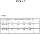
- FIG. 12 illustrates an example in which the memory controller 120 determines a standard deviation of a threshold voltage distribution among a plurality of standard deviations included in a target standard deviation list.
- FIG. 10 is a diagram illustrating an example in which the memory system 100 according to embodiments of the present disclosure determines a magnitude in which a read bias is updated according to a standard deviation.
- a threshold voltage distribution of a memory cell having a value of 1 is determined to be PV 1 ′ and a threshold voltage distribution of a memory cell having a value of 0 is determined to be PV 2 ′.
- FIG. 10 illustrates a case where a value of a standard deviation ⁇ of the threshold voltage distribution PV 1 ′ is equal to a first value ⁇ 1.
- FIG. 11 is a diagram illustrating another example in which the memory system 100 according to embodiments of the present disclosure determines a magnitude by which a read bias is updated according to a standard deviation.
- a threshold voltage distribution of a memory cell having a value of 1 is determined to be PV 1 ′′ and a threshold voltage distribution of a memory cell having a value of 0 is determined to be PV 2 ′′.
- FIG. 11 illustrates a case where a value of a standard deviation ⁇ of the threshold voltage distribution PV 1 ′′ is equal to a second value ⁇ 2 greater than the first value ⁇ 1.
- the memory controller 120 may determine the above-described first standard deviation and second standard deviation among a plurality of standard deviations included in the expected standard deviation group.
- the plurality of standard deviation values included in the expected standard deviation group may be predetermined values or values calculated by the memory controller 120 at a specific time point (e.g., when the memory device 110 is in an idle state).
- the memory controller 120 may determine the first standard deviation and the second standard deviation from the expected standard deviation group according to predetermined criteria.
- the memory controller 120 may determine the first standard deviation and the second standard deviation from the predicted standard deviation group based on a program-erase count for the target memory cell TGT_MC, a retention time for the target memory cell TGT_MC, or both.
- the program-erase count for the target memory cell TGT_MC is information indicating how many times a memory block including the target memory cell TGT_MC has been programmed and then erased from a predetermined reference time point. As the program-erase count for the target memory cell TGT_MC increases, the threshold voltage distribution of the target memory cell TGT_MC deteriorates so that the magnitude of the standard deviation increases.
- the retention time for the target memory cell TGT_MC is information indicating how much time has passed since the target memory cell TGT_MC was programmed. As the retention time for the target memory cell TGT_MC increases, the threshold voltage distribution of the target memory cell TGT_MC deteriorates so that the magnitude of the standard deviation increases.
- FIG. 12 is a diagram illustrating an example in which the memory system 100 according to embodiments of the present disclosure determines a standard deviation according to a program-erase count and a retention time.
- a standard deviation may be determined according to a range to which a value of the program-erase count belongs and a range to which a value of the retention time belongs.
- the unit of the retention time is seconds (s). Rows in FIG. 12 correspond to program-erase count ranges, and columns in FIG. 12 correspond to retention time ranges.
- the standard deviation may be determined as 0.28 corresponding to a range P 2 to which a value of 13 of the program-erase count belongs and a range R 3 to which a value of 25 seconds of the retention time belongs.
- the standard deviation may be determined as 0.25 corresponding to a range P 1 to which a value of 8 of the program-erase count belongs and a range R 4 to which a value of 37 seconds of the retention time belongs.
- the read bias of the target memory cell TGT_MC may not be able to be updated based only on the above-described ratio of the result data RESULT DATA to the number of corrected data bits.
- FIGS. 13 to 14 illustrate an example in which the read bias is updated when the target memory cell TGT_MC is the multi-level cell MLC.
- FIG. 13 is a diagram illustrating an example in which the memory system 100 according to embodiments of the present disclosure updates a plurality of read biases.
- the target memory cell TGT_MC may have four threshold voltage distributions PV 21 , PV 22 , PV 23 , and PV 24 .
- a memory cell included in the threshold voltage distribution PV 21 is a memory cell in which a most significant bit (MSB) is programmed as 1 and a least significant bit (LSB) is programmed as 1.
- a memory cell included in the threshold voltage distribution PV 22 is a memory cell in which the MSB is programmed as 1 and the LSB is programmed as 0.
- a memory cells included in the threshold voltage distribution PV 23 is a memory cell in which the MSB is programmed as 0 and the LSB is programmed as 0.
- a memory cell included in the threshold voltage distribution PV 24 is a memory cell in which the MSB is programmed as 0 and the LSB is programmed as 1.
- the memory controller 120 reads an LSB among data bits of 2 bits from the plurality of target memory cells TGT_MC.
- the threshold voltage of the memory cell when the threshold voltage of the memory cell is less than a read bias RB 31 or the threshold voltage of the memory cell is greater than a read bias RB 33 , the LSB of the memory cell is read as 1.
- the threshold voltage of the memory cell in which the LSB is programmed as 1 may be included in the threshold voltage distribution PV 21 or the threshold voltage distribution PV 24 .
- the memory controller 120 may not be able to determine how to update the read bias RB 31 and the read bias RB 33 based only on information on the number of data bits having an LSB of 1 and the number of corrected data bits among the result data RESULT_DATA. This is because the memory cell may be included in the threshold voltage distribution PV 21 but may have a threshold voltage greater than the read bias RB 31 , or the memory cell may be included in the threshold voltage distribution PV 24 but may have a threshold voltage smaller than the read bias RB 33 .
- the memory controller 120 may update the read biases RB 31 and RB 33 using information obtained by dividing the result data RESULT_DATA into i) a data bit group corresponding to the read bias RB 31 and ii) a data bit group corresponding to the read bias RB 33 .
- the above-described divided information may be generated by the memory device 110 as part of a process of reading data from the target memory cell TGT_MC.
- a group of data bits read based on the read bias RB 31 may be used to update the read bias RB 31 to RB 31 ′
- a group of data bits read based on the read bias RB 33 may be used to update the read bias RB 33 to RB 33 ′.
- the method of determining the magnitude and direction in which the read biases RB 31 and RB 33 are updated is otherwise the same as the method described above with reference to FIGS. 6 to 12 .
- the number of data bits having an LSB of 1 among the result data RESULT_DATA is 1000. If the memory controller 120 obtains, from the memory device 110 , first information indicating that the number of bits of a data bit group corresponding to the read bias RB 31 is 400 and the number of corrected data bits among those 400 bits is 5, and second information indicating that the number of bits of a data bit group corresponding to the read bias RB 33 is 600 and the number of corrected data bits among those 600 bits is 10, the read bias RB 31 may be updated based on the first information and the read bias RB 33 may be updated based on the second information.
- the memory controller 120 in order for the memory controller 120 to accurately update the read bias RB 31 , information about the number of memory cells included in the threshold voltage distribution PV 22 (that is, the number of cells programmed with an MSB of 1 and an LSB of 0) is additionally required. In addition, in order for the memory controller 120 to accurately update the read bias RB 33 , information about the number of memory cells included in the threshold voltage distribution PV 23 (that is, the number of cells programmed with an MSB of 0 and an LSB of 0) is additionally required.
- the threshold voltage of the memory cell having an LSB of 0 may be included in the threshold voltage distribution PV 22 or may be included in the threshold voltage distribution PV 23 . Therefore, the memory controller 120 may not be able to determine the number of memory cells included in the threshold voltage distribution PV 22 and the number of memory cells included in the threshold voltage distribution PV 23 from only the number of memory cells having an LSB of 0.
- the memory controller 120 may assume that the number of memory cells included in the threshold voltage distribution PV 22 and the number of memory cells included in the threshold voltage distribution PV 23 are the same.
- the memory controller 120 may obtain additional information for determining the number of memory cells included in the threshold voltage distribution PV 22 and the number of memory cells included in the threshold voltage distribution PV 23 .
- FIG. 14 is a diagram illustrating an example in which the memory system 100 of FIG. 13 updates a plurality of read biases using additional information.
- the memory controller 120 may read MSBs for the plurality of target memory cells TGT_MC to obtain additional information about the number of memory cells having an MSB of 1 and the number of memory cells having an MSB of 0. For example, the memory controller 120 may obtain this information from the memory device 110 .
- the number of memory cells included in the threshold voltage distribution PV 22 may be obtained by excluding the number of memory cells having an LSB of 1, that is, the number of data bits included in the data bit group corresponding to the read bias RB 31 , from the number of memory cells having an MSB of 1.
- the number of memory cells included in the threshold voltage distribution PV 23 may be obtained by excluding the number of memory cells having an LSB of 1, that is, the number of data bits included in the data bit group corresponding to the read bias RB 33 , from the number of memory cells having an MSB of 0.
- the memory controller 120 may determine the number of memory cells included in the threshold voltage distribution PV 22 and the number of memory cells included in the threshold voltage distribution PV 23 , and may therefore accurately update the above-described read bias RB 31 and read bias RB 33 .
- the memory controller 120 may use the number of memory cells included in the threshold voltage distribution PV 22 and the number of memory cells included in the threshold voltage distribution PV 23 and the number of data bits having a corrected MSB to update the read biases RB 32 to RB 32 ′.
- FIG. 15 illustrates time points at which the memory system 100 according to an embodiment of the present disclosure updates a read bias.
- the memory controller 120 may determine to update the read bias every time ECC decoding succeeds. When the ECC decoding fails, the memory controller 120 does not update the read bias. Instead, the memory controller 120 may always update the read bias every time the ECC decoding succeeds, thereby maintaining the read bias in an optimized state.
- the overhead required for the memory controller 120 to update the read bias may increase.
- the memory controller 120 may update the read bias only when it is determined that a currently configured read bias value is incorrect and there is a high possibility that the ECC decoding will fail later.
- FIG. 16 illustrates time points at which the memory system 100 according to another embodiment of the present disclosure updates a read bias.
- the memory controller 120 may determine to update the read bias if the number of data bits corrected during the ECC decoding is greater than or equal to a predetermined threshold number of data bits.
- the memory controller 120 may operate under the hypothesis that the number of data bits corrected during the ECC decoding became large because the currently configured read bias value is inaccurate.
- the threshold number of data bits is configured to be 10, but embodiments are not limited thereto.
- the memory controller 120 does not update the read bias because 8 ⁇ 10.
- the memory controller 120 does not update the read bias because 4 ⁇ 10.
- the memory controller 120 does not update the read bias because 7 ⁇ 10.
- FIG. 17 illustrates time points at which the memory system 100 according to still another embodiment of the present disclosure updates a read bias.
- the memory controller 120 may determine to update the read bias if the number of times (iteration) a decoding operation of the ECC decoding was repeated is greater than or equal to the predetermined threshold number of iterations.
- the memory controller 120 may correct some of the data bits from 1 to 0 or 0 to 1 while repeating the decoding operation until the ECC decoding succeeds during the ECC decoding or it is determined that decoding is impossible. If the number of times the decoding operation is repeated during the ECC decoding is large, the memory controller 120 may determine that the number of times the decoding operation is repeated during the ECC decoding is large because the currently configured read bias value is incorrect.
- the threshold number of iterations is configured to be 5, but embodiments are not limited thereto.
- the memory controller 120 does not update the read bias because 3 ⁇ 5.
- the memory controller 120 does not update the read bias because 4 ⁇ 5.
- the memory controller 120 does not update the read bias because 1 ⁇ 5.
- FIG. 18 is a flowchart illustrating a process 1800 of operating the memory system 100 according to embodiments of the present disclosure.
- operation S 1810 the process 1800 of operating the memory system 100 performs ECC decoding on read data read from a plurality of target memory cells included in the memory device 110 .
- the process 1800 determines whether to update one or more read biases used for reading data programmed in the plurality of target memory cells.
- the process 1800 updates the read bias based on information regarding: i) result data RESULT_DATA generated by the ECC decoding and ii) the number of data bits corrected during the ECC decoding.
- the memory system 100 may determine a direction in which the read bias is updated based on a first fail bit rate and a second fail bit rate.
- the first fail bit rate may be determined as a ratio of the number of data bits having a value of 1 among the result data RESULT_DATA to the number of data bits having a value corrected from 0 to 1 during the ECC decoding.
- the second fail bit rate may be determined as a ratio of the number of data bits having a value of 0 among the result data RESULT_DATA to the number of data bits having a value corrected from 1 to 0 during the ECC decoding.
- the memory system 100 may determine a magnitude in which the read bias is updated based on a first standard deviation and a second standard deviation.
- the first standard deviation may be an expected standard deviation for a threshold voltage distribution of a memory cell having a value of 1 among the plurality of target memory cells
- the second standard deviation may be an expected standard deviation for a threshold voltage distribution of a memory cell having a value of zero among the target memory cells.
- the memory system 100 may determine the first standard deviation and second standard deviation from a plurality of standard deviations included in a predicted standard deviation group based on a program-erase count for a target memory cell, a retention time for the target memory cell, or both.
- the operation of the memory controller 120 described above may be controlled by the control circuit 123 , and may be performed in a manner in which the processor 124 executes (drives) firmware in which various operations of the memory controller 120 are programmed.
- FIG. 19 is a diagram illustrating the configuration of a computing system 1900 according to an embodiment of the present disclosure.
- the computing system 1900 may include: a memory system 100 electrically connected to a system bus 1960 ; a CPU 1910 configured to control the overall operation of the computing system 1900 ; a RAM 1920 configured to store data and information related to operations of the computing system 1900 ; a user interface/user experience (UI/UX) module 1930 configured to provide the user with a user environment; a communication module 1940 configured to communicate with an external device in a wired and/or wireless type; and a power management module 1950 configured to manage power used by the computing system 1900 .
- a memory system 100 electrically connected to a system bus 1960 ; a CPU 1910 configured to control the overall operation of the computing system 1900 ; a RAM 1920 configured to store data and information related to operations of the computing system 1900 ; a user interface/user experience (UI/UX) module 1930 configured to provide the user with a user environment; a communication module 1940 configured to communicate with an external device in a wired and/or wireless type; and a power management module 1950 configured to manage power used by the computing system 1900 .
- the computing system 1900 may be a personal computer (PC) or may include a mobile terminal such as a smartphone, a tablet or various electronic devices.
- PC personal computer
- mobile terminal such as a smartphone, a tablet or various electronic devices.
- the computing system 1900 may further include a battery for supplying an operating voltage, and may further include an application chipset, a graphic-related module, a camera image processor, and a DRAM. Other elements would be obvious to a person skilled in the art.
- the memory system 100 may include not only a device configured to store data in a magnetic disk such as a hard disk drive (HDD), but also a device configured to store data in a nonvolatile memory such as a solid state drive (SSD), a universal flash storage device, or an embedded MMC (eMMC) device.
- the non-volatile memory may include a read only memory (ROM), a programmable ROM (PROM), an electrically programmable ROM (EPROM), an electrically erasable and programmable ROM (EEPROM), a flash memory, a phase-change RAM (PRAM), a magnetic RAM (MRAM), a resistive RAM (RRAM), a ferroelectric RAM (FRAM), and the like.
- the memory system 100 may be implemented as storage devices of various types and mounted inside various electronic devices.
- the operation delay time of the memory system may be minimized by reducing a number of bits that need to be corrected by an ECC decoder.
- an overhead occurring in the process of calling a specific function may be minimized.
Landscapes
- Engineering & Computer Science (AREA)
- Theoretical Computer Science (AREA)
- Physics & Mathematics (AREA)
- General Engineering & Computer Science (AREA)
- General Physics & Mathematics (AREA)
- Quality & Reliability (AREA)
- Human Computer Interaction (AREA)
- Read Only Memory (AREA)
Abstract
Description
Claims (16)
Applications Claiming Priority (2)
| Application Number | Priority Date | Filing Date | Title |
|---|---|---|---|
| KR10-2019-0171470 | 2019-12-20 | ||
| KR1020190171470A KR102816386B1 (en) | 2019-12-20 | 2019-12-20 | Memory system, memory controller, and operating method of memory system |
Publications (2)
| Publication Number | Publication Date |
|---|---|
| US20210193246A1 US20210193246A1 (en) | 2021-06-24 |
| US11238952B2 true US11238952B2 (en) | 2022-02-01 |
Family
ID=76383109
Family Applications (1)
| Application Number | Title | Priority Date | Filing Date |
|---|---|---|---|
| US16/875,358 Active US11238952B2 (en) | 2019-12-20 | 2020-05-15 | Memory system, memory controller, and method of operating memory system |
Country Status (3)
| Country | Link |
|---|---|
| US (1) | US11238952B2 (en) |
| KR (1) | KR102816386B1 (en) |
| CN (1) | CN113010459A (en) |
Families Citing this family (6)
| Publication number | Priority date | Publication date | Assignee | Title |
|---|---|---|---|---|
| KR20220103205A (en) * | 2017-12-29 | 2022-07-21 | 마이크론 테크놀로지, 인크. | Uncorrectable ecc |
| US11386972B2 (en) * | 2020-01-30 | 2022-07-12 | Macronix International Co., Ltd. | Determining read voltages for memory systems with machine learning |
| JP2022067002A (en) * | 2020-10-19 | 2022-05-02 | ソニーセミコンダクタソリューションズ株式会社 | Memory cell array unit |
| US11461025B2 (en) | 2020-11-05 | 2022-10-04 | Macronix International Co., Ltd. | Data retention in memory devices |
| KR20230034524A (en) * | 2021-09-03 | 2023-03-10 | 에스케이하이닉스 주식회사 | Memory system and operating method of memory system |
| KR102865399B1 (en) * | 2023-12-13 | 2025-09-26 | 에스케이하이닉스 주식회사 | Fail classification device for a plurality of memory cells and operation method thereof |
Citations (9)
| Publication number | Priority date | Publication date | Assignee | Title |
|---|---|---|---|---|
| US20080077841A1 (en) * | 2006-09-27 | 2008-03-27 | Gonzalez Carlos J | Methods of Cell Population Distribution Assisted Read Margining |
| US20080158958A1 (en) * | 2006-12-17 | 2008-07-03 | Anobit Technologies Ltd. | Memory device with reduced reading |
| US20090043951A1 (en) * | 2007-08-06 | 2009-02-12 | Anobit Technologies Ltd. | Programming schemes for multi-level analog memory cells |
| US20100091535A1 (en) * | 2007-03-12 | 2010-04-15 | Anobit Technologies Ltd | Adaptive estimation of memory cell read thresholds |
| US8694854B1 (en) * | 2010-08-17 | 2014-04-08 | Apple Inc. | Read threshold setting based on soft readout statistics |
| US20170163288A1 (en) * | 2015-12-08 | 2017-06-08 | Apple Inc. | On-the-fly evaluation of the number of errors corrected in iterative ecc decoding |
| KR20170097267A (en) | 2016-02-17 | 2017-08-28 | 삼성전자주식회사 | Data storage device including read voltage search unit |
| KR20190022987A (en) | 2017-08-25 | 2019-03-07 | 에스케이하이닉스 주식회사 | Data storage device and operating method thereof |
| US20200218661A1 (en) * | 2019-01-07 | 2020-07-09 | SK Hynix Inc. | Data storage device, operation method thereof, and controller therefor |
Family Cites Families (1)
| Publication number | Priority date | Publication date | Assignee | Title |
|---|---|---|---|---|
| US7817469B2 (en) | 2004-07-26 | 2010-10-19 | Sandisk Il Ltd. | Drift compensation in a flash memory |
-
2019
- 2019-12-20 KR KR1020190171470A patent/KR102816386B1/en active Active
-
2020
- 2020-05-15 US US16/875,358 patent/US11238952B2/en active Active
- 2020-07-01 CN CN202010626198.XA patent/CN113010459A/en not_active Withdrawn
Patent Citations (9)
| Publication number | Priority date | Publication date | Assignee | Title |
|---|---|---|---|---|
| US20080077841A1 (en) * | 2006-09-27 | 2008-03-27 | Gonzalez Carlos J | Methods of Cell Population Distribution Assisted Read Margining |
| US20080158958A1 (en) * | 2006-12-17 | 2008-07-03 | Anobit Technologies Ltd. | Memory device with reduced reading |
| US20100091535A1 (en) * | 2007-03-12 | 2010-04-15 | Anobit Technologies Ltd | Adaptive estimation of memory cell read thresholds |
| US20090043951A1 (en) * | 2007-08-06 | 2009-02-12 | Anobit Technologies Ltd. | Programming schemes for multi-level analog memory cells |
| US8694854B1 (en) * | 2010-08-17 | 2014-04-08 | Apple Inc. | Read threshold setting based on soft readout statistics |
| US20170163288A1 (en) * | 2015-12-08 | 2017-06-08 | Apple Inc. | On-the-fly evaluation of the number of errors corrected in iterative ecc decoding |
| KR20170097267A (en) | 2016-02-17 | 2017-08-28 | 삼성전자주식회사 | Data storage device including read voltage search unit |
| KR20190022987A (en) | 2017-08-25 | 2019-03-07 | 에스케이하이닉스 주식회사 | Data storage device and operating method thereof |
| US20200218661A1 (en) * | 2019-01-07 | 2020-07-09 | SK Hynix Inc. | Data storage device, operation method thereof, and controller therefor |
Also Published As
| Publication number | Publication date |
|---|---|
| KR20210079555A (en) | 2021-06-30 |
| CN113010459A (en) | 2021-06-22 |
| KR102816386B1 (en) | 2025-06-04 |
| US20210193246A1 (en) | 2021-06-24 |
Similar Documents
| Publication | Publication Date | Title |
|---|---|---|
| US11238952B2 (en) | Memory system, memory controller, and method of operating memory system | |
| US11321170B2 (en) | Memory system, memory controller, and method for operating memory system | |
| US11301174B2 (en) | Memory system, memory controller and method for operating memory system | |
| US11630764B2 (en) | Memory system, memory controller, and method for operating same | |
| US11500563B2 (en) | Memory system and operating method for testing target firmware by processing a plurality of test commands | |
| US20250117327A1 (en) | Memory system, memory controller and operating method of the memory system for controlling garbage collection | |
| US11656790B2 (en) | Memory system, memory controller, and operation method of memory system | |
| US11216208B1 (en) | Memory system, memory controller, and operation method of memory system | |
| US11307807B2 (en) | Memory system, memory controller, and method for operating memory system for determining read biases for read retry operation | |
| US11327902B2 (en) | Memory system, memory controller, and operation method of memory system for setting lock on map segments cached in map cache | |
| US11137942B2 (en) | Memory system, memory controller, and method of operating a memory system for determining a number of hit and miss requests about map segments in a map cache and determining whether or not to perform data read operation in parallel | |
| US11372766B2 (en) | Memory system, memory controller, and method of operating memory system | |
| US11315650B2 (en) | Memory system, memory controller, and method of operating memory system | |
| US11386000B2 (en) | Memory system, memory controller and method for operating memory system in which different processors search for mapping information using different map search engines | |
| US12422996B2 (en) | Controller for controlling one-time programmable memory, system, and operation method thereof | |
| US11848054B2 (en) | Memory device determining precharge time based on a number of times that a program voltage is applied to word line and operating method of memory device | |
| US11507509B2 (en) | Memory system, memory controller and method for operating memory system for determining whether to perform direct write based on reference write size | |
| US11495319B2 (en) | Memory system, memory controller, and method for operating memory system performing integrity check operation on target code when voltage drop is detected | |
| US11544003B2 (en) | Memory system, memory controller, and method of operating memory system | |
| US12197770B2 (en) | Memory system, memory controller, and operation method of memory system | |
| US12189474B2 (en) | Controller and operating method of the controller for determining reliability data based on syndrome weight | |
| US11775190B2 (en) | Memory system and operating method of memory system | |
| US12056047B2 (en) | Memory system, memory controller and operating method thereof for determining garbage collection victim block |
Legal Events
| Date | Code | Title | Description |
|---|---|---|---|
| FEPP | Fee payment procedure |
Free format text: ENTITY STATUS SET TO UNDISCOUNTED (ORIGINAL EVENT CODE: BIG.); ENTITY STATUS OF PATENT OWNER: LARGE ENTITY |
|
| AS | Assignment |
Owner name: SK HYNIX INC., KOREA, REPUBLIC OF Free format text: ASSIGNMENT OF ASSIGNORS INTEREST;ASSIGNORS:JO, MYUNG JIN;KIM, DAE SUNG;REEL/FRAME:052686/0848 Effective date: 20200508 |
|
| STPP | Information on status: patent application and granting procedure in general |
Free format text: NON FINAL ACTION MAILED |
|
| STPP | Information on status: patent application and granting procedure in general |
Free format text: RESPONSE TO NON-FINAL OFFICE ACTION ENTERED AND FORWARDED TO EXAMINER |
|
| STPP | Information on status: patent application and granting procedure in general |
Free format text: NOTICE OF ALLOWANCE MAILED -- APPLICATION RECEIVED IN OFFICE OF PUBLICATIONS |
|
| STPP | Information on status: patent application and granting procedure in general |
Free format text: PUBLICATIONS -- ISSUE FEE PAYMENT VERIFIED |
|
| STCF | Information on status: patent grant |
Free format text: PATENTED CASE |
|
| MAFP | Maintenance fee payment |
Free format text: PAYMENT OF MAINTENANCE FEE, 4TH YEAR, LARGE ENTITY (ORIGINAL EVENT CODE: M1551); ENTITY STATUS OF PATENT OWNER: LARGE ENTITY Year of fee payment: 4 |