US11230762B2 - Film structure reproduction method and reproduction film structure - Google Patents
Film structure reproduction method and reproduction film structure Download PDFInfo
- Publication number
- US11230762B2 US11230762B2 US16/615,703 US201916615703A US11230762B2 US 11230762 B2 US11230762 B2 US 11230762B2 US 201916615703 A US201916615703 A US 201916615703A US 11230762 B2 US11230762 B2 US 11230762B2
- Authority
- US
- United States
- Prior art keywords
- film structure
- new
- film
- active surface
- reproduction
- Prior art date
- Legal status (The legal status is an assumption and is not a legal conclusion. Google has not performed a legal analysis and makes no representation as to the accuracy of the status listed.)
- Active
Links
Images


Classifications
-
- H—ELECTRICITY
- H01—ELECTRIC ELEMENTS
- H01J—ELECTRIC DISCHARGE TUBES OR DISCHARGE LAMPS
- H01J37/00—Discharge tubes with provision for introducing objects or material to be exposed to the discharge, e.g. for the purpose of examination or processing thereof
- H01J37/32—Gas-filled discharge tubes
- H01J37/32431—Constructional details of the reactor
- H01J37/32623—Mechanical discharge control means
- H01J37/32642—Focus rings
-
- H—ELECTRICITY
- H10—SEMICONDUCTOR DEVICES; ELECTRIC SOLID-STATE DEVICES NOT OTHERWISE PROVIDED FOR
- H10P—GENERIC PROCESSES OR APPARATUS FOR THE MANUFACTURE OR TREATMENT OF DEVICES COVERED BY CLASS H10
- H10P14/00—Formation of materials, e.g. in the shape of layers or pillars
- H10P14/60—Formation of materials, e.g. in the shape of layers or pillars of insulating materials
- H10P14/63—Formation of materials, e.g. in the shape of layers or pillars of insulating materials characterised by the formation processes
- H10P14/6326—Deposition processes
- H10P14/6328—Deposition from the gas or vapour phase
- H10P14/6334—Deposition from the gas or vapour phase using decomposition or reaction of gaseous or vapour phase compounds, i.e. chemical vapour deposition
-
- C—CHEMISTRY; METALLURGY
- C23—COATING METALLIC MATERIAL; COATING MATERIAL WITH METALLIC MATERIAL; CHEMICAL SURFACE TREATMENT; DIFFUSION TREATMENT OF METALLIC MATERIAL; COATING BY VACUUM EVAPORATION, BY SPUTTERING, BY ION IMPLANTATION OR BY CHEMICAL VAPOUR DEPOSITION, IN GENERAL; INHIBITING CORROSION OF METALLIC MATERIAL OR INCRUSTATION IN GENERAL
- C23C—COATING METALLIC MATERIAL; COATING MATERIAL WITH METALLIC MATERIAL; SURFACE TREATMENT OF METALLIC MATERIAL BY DIFFUSION INTO THE SURFACE, BY CHEMICAL CONVERSION OR SUBSTITUTION; COATING BY VACUUM EVAPORATION, BY SPUTTERING, BY ION IMPLANTATION OR BY CHEMICAL VAPOUR DEPOSITION, IN GENERAL
- C23C16/00—Chemical coating by decomposition of gaseous compounds, without leaving reaction products of surface material in the coating, i.e. chemical vapour deposition [CVD] processes
- C23C16/22—Chemical coating by decomposition of gaseous compounds, without leaving reaction products of surface material in the coating, i.e. chemical vapour deposition [CVD] processes characterised by the deposition of inorganic material, other than metallic material
- C23C16/30—Deposition of compounds, mixtures or solid solutions, e.g. borides, carbides, nitrides
- C23C16/32—Carbides
- C23C16/325—Silicon carbide
-
- C—CHEMISTRY; METALLURGY
- C23—COATING METALLIC MATERIAL; COATING MATERIAL WITH METALLIC MATERIAL; CHEMICAL SURFACE TREATMENT; DIFFUSION TREATMENT OF METALLIC MATERIAL; COATING BY VACUUM EVAPORATION, BY SPUTTERING, BY ION IMPLANTATION OR BY CHEMICAL VAPOUR DEPOSITION, IN GENERAL; INHIBITING CORROSION OF METALLIC MATERIAL OR INCRUSTATION IN GENERAL
- C23C—COATING METALLIC MATERIAL; COATING MATERIAL WITH METALLIC MATERIAL; SURFACE TREATMENT OF METALLIC MATERIAL BY DIFFUSION INTO THE SURFACE, BY CHEMICAL CONVERSION OR SUBSTITUTION; COATING BY VACUUM EVAPORATION, BY SPUTTERING, BY ION IMPLANTATION OR BY CHEMICAL VAPOUR DEPOSITION, IN GENERAL
- C23C16/00—Chemical coating by decomposition of gaseous compounds, without leaving reaction products of surface material in the coating, i.e. chemical vapour deposition [CVD] processes
- C23C16/44—Chemical coating by decomposition of gaseous compounds, without leaving reaction products of surface material in the coating, i.e. chemical vapour deposition [CVD] processes characterised by the method of coating
- C23C16/4401—Means for minimising impurities, e.g. dust, moisture or residual gas, in the reaction chamber
- C23C16/4404—Coatings or surface treatment on the inside of the reaction chamber or on parts thereof
-
- C—CHEMISTRY; METALLURGY
- C23—COATING METALLIC MATERIAL; COATING MATERIAL WITH METALLIC MATERIAL; CHEMICAL SURFACE TREATMENT; DIFFUSION TREATMENT OF METALLIC MATERIAL; COATING BY VACUUM EVAPORATION, BY SPUTTERING, BY ION IMPLANTATION OR BY CHEMICAL VAPOUR DEPOSITION, IN GENERAL; INHIBITING CORROSION OF METALLIC MATERIAL OR INCRUSTATION IN GENERAL
- C23C—COATING METALLIC MATERIAL; COATING MATERIAL WITH METALLIC MATERIAL; SURFACE TREATMENT OF METALLIC MATERIAL BY DIFFUSION INTO THE SURFACE, BY CHEMICAL CONVERSION OR SUBSTITUTION; COATING BY VACUUM EVAPORATION, BY SPUTTERING, BY ION IMPLANTATION OR BY CHEMICAL VAPOUR DEPOSITION, IN GENERAL
- C23C16/00—Chemical coating by decomposition of gaseous compounds, without leaving reaction products of surface material in the coating, i.e. chemical vapour deposition [CVD] processes
- C23C16/44—Chemical coating by decomposition of gaseous compounds, without leaving reaction products of surface material in the coating, i.e. chemical vapour deposition [CVD] processes characterised by the method of coating
- C23C16/458—Chemical coating by decomposition of gaseous compounds, without leaving reaction products of surface material in the coating, i.e. chemical vapour deposition [CVD] processes characterised by the method of coating characterised by the method used for supporting substrates in the reaction chamber
-
- H—ELECTRICITY
- H01—ELECTRIC ELEMENTS
- H01J—ELECTRIC DISCHARGE TUBES OR DISCHARGE LAMPS
- H01J37/00—Discharge tubes with provision for introducing objects or material to be exposed to the discharge, e.g. for the purpose of examination or processing thereof
- H01J37/32—Gas-filled discharge tubes
- H01J37/32431—Constructional details of the reactor
- H01J37/32458—Vessel
- H01J37/32477—Vessel characterised by the means for protecting vessels or internal parts, e.g. coatings
- H01J37/32495—Means for protecting the vessel against plasma
-
- H—ELECTRICITY
- H10—SEMICONDUCTOR DEVICES; ELECTRIC SOLID-STATE DEVICES NOT OTHERWISE PROVIDED FOR
- H10P—GENERIC PROCESSES OR APPARATUS FOR THE MANUFACTURE OR TREATMENT OF DEVICES COVERED BY CLASS H10
- H10P14/00—Formation of materials, e.g. in the shape of layers or pillars
- H10P14/20—Formation of materials, e.g. in the shape of layers or pillars of semiconductor materials
- H10P14/34—Deposited materials, e.g. layers
- H10P14/3402—Deposited materials, e.g. layers characterised by the chemical composition
- H10P14/3404—Deposited materials, e.g. layers characterised by the chemical composition being Group IVA materials
- H10P14/3408—Silicon carbide
-
- H—ELECTRICITY
- H10—SEMICONDUCTOR DEVICES; ELECTRIC SOLID-STATE DEVICES NOT OTHERWISE PROVIDED FOR
- H10P—GENERIC PROCESSES OR APPARATUS FOR THE MANUFACTURE OR TREATMENT OF DEVICES COVERED BY CLASS H10
- H10P14/00—Formation of materials, e.g. in the shape of layers or pillars
- H10P14/60—Formation of materials, e.g. in the shape of layers or pillars of insulating materials
- H10P14/69—Inorganic materials
- H10P14/6903—Inorganic materials containing silicon
- H10P14/6905—Inorganic materials containing silicon being a silicon carbide or silicon carbonitride and not containing oxygen, e.g. SiC or SiC:H
-
- H—ELECTRICITY
- H10—SEMICONDUCTOR DEVICES; ELECTRIC SOLID-STATE DEVICES NOT OTHERWISE PROVIDED FOR
- H10P—GENERIC PROCESSES OR APPARATUS FOR THE MANUFACTURE OR TREATMENT OF DEVICES COVERED BY CLASS H10
- H10P50/00—Etching of wafers, substrates or parts of devices
- H10P50/20—Dry etching; Plasma etching; Reactive-ion etching
- H10P50/24—Dry etching; Plasma etching; Reactive-ion etching of semiconductor materials
- H10P50/242—Dry etching; Plasma etching; Reactive-ion etching of semiconductor materials of Group IV materials
-
- H—ELECTRICITY
- H10—SEMICONDUCTOR DEVICES; ELECTRIC SOLID-STATE DEVICES NOT OTHERWISE PROVIDED FOR
- H10P—GENERIC PROCESSES OR APPARATUS FOR THE MANUFACTURE OR TREATMENT OF DEVICES COVERED BY CLASS H10
- H10P50/00—Etching of wafers, substrates or parts of devices
- H10P50/20—Dry etching; Plasma etching; Reactive-ion etching
- H10P50/28—Dry etching; Plasma etching; Reactive-ion etching of insulating materials
- H10P50/282—Dry etching; Plasma etching; Reactive-ion etching of insulating materials of inorganic materials
- H10P50/283—Dry etching; Plasma etching; Reactive-ion etching of insulating materials of inorganic materials by chemical means
Definitions
- the present invention relates to reproduction of a structure configured by forming a film containing SiC, and more particularly, to a reproduction method and a reproduction structure suitable for reducing a reproduction cost of the film structure.
- Patent Document 1 Japanese Unexamined Patent Application Publication No. 2012-49220
- Patent Document 2 Japanese Unexamined Patent Application Publication No. 2017-212427
- Patent Documents 1 and 2 it is possible to reliably obtain a reproduction member having the same quality as that of a SiC member before use.
- the new SiC layer is deposited and fabricated after various pretreatment steps such as preprocessing or cleaning for the damaged portion, and masking for a portion where the new SiC layer is not deposited. For this reason, the reproduction cost increases, so that it is difficult to find out a merit, compared to a manufacturing cost of a new product.
- a film structure reproduction method including: a new film layer deposition step of depositing a new film layer having a thickness equal to or larger than a depth of a damage by setting a surface opposite to a damaged surface as a main body formation surface; and an active surface fabrication step of fabricating the damaged surface to have a desired shape, wherein, in the active surface fabrication step, fabrication is performed until a depth at which the damaged portion is completely removed.
- the new film layer deposition step may be performed while active surfaces of two film structures come into contact or are adjacent to each other. In this characteristic, it is possible to deposit a new film layer on the non-active surface sides of the two film structures at one time.
- the film structure may be a SiC member.
- a reproduction film structure including: an active surface obtained by performing fabrication to completely remove a damaged portion on an old film layer having a damage; and a non-active surface obtained by forming a new film layer having a thickness equal to or larger than a depth of the damage on the old film layer as integrated two sides.
- FIG. 1 is a cross-sectional view illustrating a shape of a focus ring damaged by use
- FIG. 2 is a cross-sectional view illustrating a state in which a new SiC layer is formed in an outer circumference of the focus ring;
- FIG. 3 is a cross-sectional view illustrating a state in which a reference surface is formed by cutting a new SiC layer formed on a non-active surface;
- FIG. 4 is a cross-sectional view illustrating a state in which the focus ring is reproduced using a shaping frame
- FIG. 5 is a diagram illustrating a schematic configuration of a CVD film formation apparatus used in film formation of the new SiC layer
- FIG. 6 is flowchart illustrating a configuration for performing a film structure reproduction method according to a first embodiment
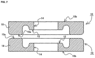
- FIG. 7 is a cross-sectional view illustrating a focus ring arrangement form for performing a film structure reproduction method according to a second embodiment
- FIG. 8 is a cross-sectional view illustrating a new SiC layer formed on each non-active surface of a pair of focus rings as a main body;
- FIG. 9 is a diagram illustrating a specific example for horizontally arranging the focus rings when the film structure reproduction method according to the second embodiment is carried out.
- FIG. 10 is a diagram illustrating a specific example for vertically arranging the focus rings when the film structure reproduction method according to the second embodiment is carried out.
- a film structure reproduction method and a reproduction film structure according to an embodiment of the present invention will now be described in details with reference to the accompanying drawings.
- the film structure reproduction method according to this embodiment is effectively applied by using a SiC member such as a jig provided in a semiconductor manufacturing chamber for plasma etching treatment or the like as a main body.
- a focus ring 10 as a SiC member used to support a wafer (not shown) for plasma etching treatment will be described as an example of the film structure according to an embodiment of the invention.
- the focus ring 10 is a support member interposed between a lower electrode and a wafer in a chamber when plasma etching is performed. For this reason, the focus ring 10 at least has a spot face (step) 12 for placing a wafer and a through-hole 14 for inserting an electrostatic chuck.
- the shape of the focus ring 10 is not limitative, but has a so-called doughnut shape in the examples of FIGS. 1 to 4 .
- a surface where the wafer is placed (active surface 10 a ) is eroded and damaged (corroded) by plasma due to influence of the plasma etching treatment.
- the damage state of the active surface 10 a is not uniform, the damage tends to increase in the outer edge portion of the step 12 adjacent to the vicinity of the outer circumference of the wafer as illustrated in FIG. 1 which shows a cross-sectional shape of the damaged focus ring. Note that the contour line indicated by the two-dotted chain line in FIG. 1 shows an external shape of the focus ring 10 before damage.
- a method of reproducing a film structure (focus ring 10 ) damaged on the active surface 10 a in this manner will be described with reference to FIGS. 1 to 4 and 5 .
- a SiC layer as a new film layer (hereinafter, referred to as a new SiC layer 16 ) is formed on a surface of the film structure having a damage on the active surface 10 a using a CVD method, particularly, a plasma CVD method in order to achieve reproduction.
- a CVD method particularly, a plasma CVD method in order to achieve reproduction.
- the film formation method may include other CVD methods such as a thermal CVD method or an optical CVD method
- the plasma CVD method is preferably employed because it facilitates high speed deposition.
- the CVD film formation apparatus 50 of FIG. 5 basically includes a chamber 52 , a source gas container 60 , and a high-frequency power source 62 .
- the chamber 52 has a shower head 54 that blasts a source gas in a plasma state and a mounting table 56 on which a film formation target (in this embodiment, the focus ring 10 ) is placed, and is installed with a vacuum pump 58 .
- valves 52 a and 52 b are provided in an inlet side (source gas supply side) and an outlet side (vacuum pump arrangement side), respectively, so that the chamber can be evacuated.
- the mounting table 56 has a heater 56 a for heating the film formation target.
- the high frequency power source 62 is an element that applies a voltage for converting the source gas supplied from the source gas container 60 into a plasma state, and a matching circuit 64 is inserted.
- the focus ring 10 as a film structure is placed on the mounting table 56 inside the chamber 52 of the CVD film formation apparatus 50 .
- the non-active surface 10 b of the focus ring 10 is set as a main body formation surface of the new SiC layer 16 .
- the active surface 10 a is arranged to face the mounting table 56 . As a result, it is difficult to perform deposition on the new SiC layer 16 in the active surface 10 a side adjacent to the mounting table 56 .
- a new SiC layer 16 is formed on the upper surface of the SiC layer included in the damaged focus ring 10 (hereinafter, referred to as an old SiC layer 18 ).
- the deposition thickness “d” of the new SiC layer 16 is not limited, but is set to at least a thickness equal to or larger than a damage depth “s” of the focus ring 10 (see FIG. 2 ).
- the new SiC layer 16 is formed to be thickest in the upper surface side of the apparatus, that is, the non-active surface 10 b side (S 10 : see FIG. 6 ).
- the focus ring 10 is extracted from the CVD film formation apparatus 50 .
- the outer circumference of the extracted focus ring 10 is cut or ground to trim the shape.
- the cutting or grinding method is not limited. However, in the case of mechanical machining, basically, a reference surface is formed, and a dimension is then set with respect to this reference surface. Then, a machining allowance is determined, and cutting or grinding for other surfaces is performed.
- the reference surface is formed by cutting or grinding the new SiC layer 16 deposited on the non-active surface 10 b side within a minimum range.
- the contour line indicated by the two-dotted chain line in FIG. 3 represents a desired outer shape of the focus ring 10 .
- the outer surface, the active surface 10 a , and the inner surface (through-hole 14 ) are fabricated to form the new focus ring 10 (reproduction film structure) of FIG. 4 .
- the fabrication of the active surface 10 a it is desirable to perform the fabrication to a depth (thickness) by which the damaged portion (corroded portion) can be completely removed. This is to prevent generation of particles caused by the brittle corroded portion when the reproduced focus ring 10 is used (S 20 : see FIG. 6 ).
- the film structure reproduction method having such characteristics, it is not necessary to fabricate or clean the damaged portion in the old film layer (the old SiC layer 18 of the embodiment) before the new film layer (the new SiC layer 16 of the embodiment) is formed. For this reason, the fabrication can be performed merely by shaping after forming the new film layer. Therefore, it is possible to easily obtain a reproduced film structure at low cost.
- the fabrication after forming the new SiC layer 16 as a new film layer on the non-active surface 10 b side it is possible to reproduce the film structure (the focus ring 10 of the embodiment) even when the damage is deep, and it is difficult to perform preliminary fabrication.
- cutting or grinding of the preliminary fabrication is performed until the damaged portion is planarized.
- the member may be damaged or bent, so that it is difficult to perform the preliminary fabrication.
- the step of forming the new film layer (new SiC layer 16 ) is performed before fabrication, it is possible to secure the thickness of the member even when the damage of the old film layer (old SiC layer 18 ) is deep. Therefore, it is possible to form the reproduction film structure (focus ring 10 ).
- a CVD method is employed as an example of the formation means of the new SiC layer 16 .
- a physical vapor deposition (PVD) method such as vacuum deposition or sputtering may be employed. This is because the film structure reproduction method according to the present invention can be performed if the new SiC layer 16 can be formed on the non-active surface 10 b side of the old SiC layer 18 .
- FIGS. 7 and 8 a film structure reproduction method according to a second embodiment of the present invention will be described with reference to FIGS. 7 and 8 .
- the film structure reproduction method according to this embodiment has a basic step similar to that of the film structure reproduction method of the first embodiment described above.
- the film structure reproduction method according to the second embodiment is different from that of the first embodiment in that a step of forming two film structures as a pair of new film layers is performed.
- two focus rings 10 as film structures are arranged such that their active surfaces 10 a face each other.
- the active surfaces 10 a of the two focus rings 10 have a contact state or an adjacent state.
- the new SiC layer 16 is formed by arranging a pair of focus rings 10 in this state in the chamber of the CVD film formation apparatus 50 .
- the new SiC layer 16 formed on the non-active surface 10 b can be made thicker than that formed on the active surface 10 a as illustrated in FIG. 8 .
- the fabrication step and the cleaning step after the deposition step of the new SiC layer 16 are similar to those of the film structure reproduction method of the first embodiment described above.
- the fabrication step and the cleaning step are performed for each focus ring 10 .
- the focus rings 10 may be placed, for example, in the following way.
- the focus rings 10 arranged in a stacked manner may be placed in a floating state floating from the mounting table using an outer surface support jig 70 capable of partially supporting the outer surface of the lower focus ring 10 .
- a spacing support jig 72 may be arranged between the active surfaces 10 a of the two focus rings 10 .
- the source gas that has been converted into a plasma state also flows to the non-active surface 10 b of the lower focus ring 10 to form a new SiC layer 16 .
- a suspending jig 74 having a suspending portion 74 a arranged between the two focus rings 10 , an inner surface support portion 74 b protruding to the focus ring 10 arrangement side from the suspending portion 74 a , an active surface support portion 74 c , and the like may be used to support the focus rings 10 as illustrated in FIG. 10 .
- a placement method it is possible to deposit the new SiC layer 16 in the non-active surface 10 b sides of the two focus rings 10 .
- the new SiC layer 16 can be formed by heating the focus rings 10 using any method, employing a hot wall type CVD film formation apparatus, or employing a PVD film formation method.
- reproduction of the focus ring 10 has been described by exemplifying the focus ring 10 which is a jig used in semiconductor manufacturing as an example of the film structure.
- the film structure reproduction method according to the present invention can be applied to various film structures that may be damaged on the surface.
- the SiC member has been described by way of example on the basis of utility in terms of cost in the aforementioned embodiments, the present invention is also applicable to a film structure such as silicon (Si).
Landscapes
- Chemical & Material Sciences (AREA)
- Engineering & Computer Science (AREA)
- Chemical Kinetics & Catalysis (AREA)
- Metallurgy (AREA)
- Materials Engineering (AREA)
- Mechanical Engineering (AREA)
- General Chemical & Material Sciences (AREA)
- Organic Chemistry (AREA)
- Physics & Mathematics (AREA)
- Plasma & Fusion (AREA)
- Analytical Chemistry (AREA)
- Inorganic Chemistry (AREA)
- Chemical Vapour Deposition (AREA)
Abstract
Description
-
- 10 focus ring,
- 10 a active surface,
- 10 b non-active surface,
- 12 step,
- 14 through-hole,
- 16 new SiC layer,
- 18 old SiC layer,
- 50 CVD film formation apparatus,
- 52 chamber,
- 52 a, 52 b valve,
- 54 shower head,
- 56 mounting table,
- 56 a heater,
- 58 vacuum pump,
- 60 source gas container,
- 62 high frequency power source,
- 64 matching circuit,
- 70 outer surface support jig,
- 72 spacing support jig,
- 74 suspending jig,
- 74 a suspending portion,
- 74 b inner surface support portion,
- 74 c active surface support portion.
Claims (2)
Applications Claiming Priority (4)
| Application Number | Priority Date | Filing Date | Title |
|---|---|---|---|
| JPJP2019-110254 | 2019-06-13 | ||
| JP2019-110254 | 2019-06-13 | ||
| JP2019110254A JP6598132B1 (en) | 2019-06-13 | 2019-06-13 | Method for regenerating film forming structure and regenerating film forming structure |
| PCT/JP2019/038355 WO2020250454A1 (en) | 2019-06-13 | 2019-09-27 | Method for regenerating film formation structure and regenerated film formation structure |
Publications (2)
| Publication Number | Publication Date |
|---|---|
| US20210025054A1 US20210025054A1 (en) | 2021-01-28 |
| US11230762B2 true US11230762B2 (en) | 2022-01-25 |
Family
ID=71142143
Family Applications (1)
| Application Number | Title | Priority Date | Filing Date |
|---|---|---|---|
| US16/615,703 Active US11230762B2 (en) | 2019-06-13 | 2019-09-27 | Film structure reproduction method and reproduction film structure |
Country Status (2)
| Country | Link |
|---|---|
| US (1) | US11230762B2 (en) |
| KR (1) | KR102124738B1 (en) |
Citations (7)
| Publication number | Priority date | Publication date | Assignee | Title |
|---|---|---|---|---|
| US5254370A (en) * | 1991-06-24 | 1993-10-19 | Hoya Corporation | Method for forming a silicon carbide film |
| JP2004079983A (en) | 2002-08-20 | 2004-03-11 | Creative Technology:Kk | How to Recycle Silicon Focus Ring |
| US20040126486A1 (en) * | 2001-06-13 | 2004-07-01 | Taiji Torigoe | Method of repairing a Ni-base alloy part |
| US20100314356A1 (en) | 2009-06-12 | 2010-12-16 | Tokyo Electron Limited | Method of reusing a consumable part for use in a plasma processing apparatus |
| JP2012049220A (en) | 2010-08-25 | 2012-03-08 | Mitsui Eng & Shipbuild Co Ltd | Plasma resistant member and method for recycling the same |
| TW201546946A (en) | 2014-06-12 | 2015-12-16 | Advanced Micro Fab Equip Inc | Substrate support tray inside a plasma treatment device and operating method thereof |
| JP2017212427A (en) | 2016-05-25 | 2017-11-30 | 韓國東海炭素株式會社 | Reproduction method of semiconductor manufacturing component, its reproduction apparatus and reproduction component |
-
2019
- 2019-09-27 KR KR1020197036067A patent/KR102124738B1/en active Active
- 2019-09-27 US US16/615,703 patent/US11230762B2/en active Active
Patent Citations (12)
| Publication number | Priority date | Publication date | Assignee | Title |
|---|---|---|---|---|
| US5254370A (en) * | 1991-06-24 | 1993-10-19 | Hoya Corporation | Method for forming a silicon carbide film |
| US20040126486A1 (en) * | 2001-06-13 | 2004-07-01 | Taiji Torigoe | Method of repairing a Ni-base alloy part |
| JP2004079983A (en) | 2002-08-20 | 2004-03-11 | Creative Technology:Kk | How to Recycle Silicon Focus Ring |
| US20100314356A1 (en) | 2009-06-12 | 2010-12-16 | Tokyo Electron Limited | Method of reusing a consumable part for use in a plasma processing apparatus |
| JP2011018894A (en) | 2009-06-12 | 2011-01-27 | Tokyo Electron Ltd | Method for reusing consumable part used for plasma processing apparatus |
| US20120258258A1 (en) * | 2009-06-12 | 2012-10-11 | Tokyo Electron Limited | Method of reusing a consumable part for use in a plasma processing apparatus |
| US20130284375A1 (en) | 2009-06-12 | 2013-10-31 | Tokyo Electron Limited | Consumable part for use in a plasma processing apparatus |
| JP2012049220A (en) | 2010-08-25 | 2012-03-08 | Mitsui Eng & Shipbuild Co Ltd | Plasma resistant member and method for recycling the same |
| US20130157067A1 (en) | 2010-08-25 | 2013-06-20 | Admap Inc. | Plasma-resistant member and method for regenerating same |
| TW201546946A (en) | 2014-06-12 | 2015-12-16 | Advanced Micro Fab Equip Inc | Substrate support tray inside a plasma treatment device and operating method thereof |
| JP2017212427A (en) | 2016-05-25 | 2017-11-30 | 韓國東海炭素株式會社 | Reproduction method of semiconductor manufacturing component, its reproduction apparatus and reproduction component |
| US20170345624A1 (en) | 2016-05-25 | 2017-11-30 | Tokai Carbon Korea Co., Ltd | Method and apparatus for reproducing component of semiconductor manufacturing apparatus, and reproduced component |
Non-Patent Citations (1)
| Title |
|---|
| Mar. 30, 2020 Office Action issued in Taiwanese Patent Application No. 108140805. |
Also Published As
| Publication number | Publication date |
|---|---|
| US20210025054A1 (en) | 2021-01-28 |
| KR102124738B1 (en) | 2020-06-18 |
Similar Documents
| Publication | Publication Date | Title |
|---|---|---|
| CN113557598B (en) | SiC edge ring | |
| KR101671671B1 (en) | Reproducing method of part for semiconductor manufactoring, reproducing apparatus and reproduced part thereof | |
| US10020218B2 (en) | Substrate support assembly with deposited surface features | |
| US12142478B2 (en) | Method and chamber for backside physical vapor deposition | |
| KR100625928B1 (en) | Method and apparatus for processing semiconductor substrates | |
| CN108346611B (en) | Electrostatic chuck, method for making the same, and plasma processing device | |
| TW200901285A (en) | RF shutter | |
| TWI660247B (en) | Substrate holding member | |
| KR102262330B1 (en) | Reproducing method for semiconductor manufactoring and a reproduced part for semiconductor manufactoring | |
| TW202117918A (en) | Wafer heater with backside and integrated bevel purge | |
| US11996315B2 (en) | Thin substrate handling via edge clamping | |
| US20080024742A1 (en) | Substrate stage and heat treatment apparatus | |
| JP2023507091A (en) | A semiconductor processing chuck with recesses near the perimeter of the wafer to reduce edge/center non-uniformity | |
| JP6598132B1 (en) | Method for regenerating film forming structure and regenerating film forming structure | |
| KR20180071952A (en) | A PART FOR SEMICONDUCTOR MANUFACTORING WITH SiC DEPOSITION LAYER AND MANUFACTORING METHOD THE SAME | |
| US11230762B2 (en) | Film structure reproduction method and reproduction film structure | |
| US20240052516A1 (en) | Metal part for process chamber and method of forming thin film layer of metal part for process chamber | |
| TW202507040A (en) | Conditioning treatment for ald productivity | |
| TW202027194A (en) | Gas distribution assemblies and operation thereof | |
| FR3090615A1 (en) | Method of manufacturing a device comprising a membrane overhanging a cavity | |
| US11049747B2 (en) | SiC freestanding film structure | |
| JP3305654B2 (en) | Plasma CVD apparatus and recording medium | |
| TWI810683B (en) | Cover wafer for semiconductor processing chamber | |
| KR101238842B1 (en) | Susceptor for manufacturing semiconductor and apparatus comprising the same | |
| CN115513041A (en) | SiC substrate processing method and structure, wafer processing method |
Legal Events
| Date | Code | Title | Description |
|---|---|---|---|
| AS | Assignment |
Owner name: ADMAP INC., JAPAN Free format text: ASSIGNMENT OF ASSIGNORS INTEREST;ASSIGNOR:NAKAMURA, MASAKI;REEL/FRAME:051082/0146 Effective date: 20191010 |
|
| FEPP | Fee payment procedure |
Free format text: ENTITY STATUS SET TO UNDISCOUNTED (ORIGINAL EVENT CODE: BIG.); ENTITY STATUS OF PATENT OWNER: LARGE ENTITY |
|
| STPP | Information on status: patent application and granting procedure in general |
Free format text: NON FINAL ACTION MAILED |
|
| STPP | Information on status: patent application and granting procedure in general |
Free format text: RESPONSE TO NON-FINAL OFFICE ACTION ENTERED AND FORWARDED TO EXAMINER |
|
| STPP | Information on status: patent application and granting procedure in general |
Free format text: FINAL REJECTION MAILED |
|
| STPP | Information on status: patent application and granting procedure in general |
Free format text: DOCKETED NEW CASE - READY FOR EXAMINATION |
|
| STPP | Information on status: patent application and granting procedure in general |
Free format text: NON FINAL ACTION MAILED |
|
| STPP | Information on status: patent application and granting procedure in general |
Free format text: RESPONSE TO NON-FINAL OFFICE ACTION ENTERED AND FORWARDED TO EXAMINER |
|
| STPP | Information on status: patent application and granting procedure in general |
Free format text: NOTICE OF ALLOWANCE MAILED -- APPLICATION RECEIVED IN OFFICE OF PUBLICATIONS |
|
| STPP | Information on status: patent application and granting procedure in general |
Free format text: PUBLICATIONS -- ISSUE FEE PAYMENT VERIFIED |
|
| STCF | Information on status: patent grant |
Free format text: PATENTED CASE |
|
| MAFP | Maintenance fee payment |
Free format text: PAYMENT OF MAINTENANCE FEE, 4TH YEAR, LARGE ENTITY (ORIGINAL EVENT CODE: M1551); ENTITY STATUS OF PATENT OWNER: LARGE ENTITY Year of fee payment: 4 |