US11228335B2 - Method and apparatus for adjusting signal level in wireless communication system - Google Patents
Method and apparatus for adjusting signal level in wireless communication system Download PDFInfo
- Publication number
- US11228335B2 US11228335B2 US16/727,438 US201916727438A US11228335B2 US 11228335 B2 US11228335 B2 US 11228335B2 US 201916727438 A US201916727438 A US 201916727438A US 11228335 B2 US11228335 B2 US 11228335B2
- Authority
- US
- United States
- Prior art keywords
- signal
- mixer
- pvt
- signal level
- level
- Prior art date
- Legal status (The legal status is an assumption and is not a legal conclusion. Google has not performed a legal analysis and makes no representation as to the accuracy of the status listed.)
- Active
Links
Images


Classifications
-
- H—ELECTRICITY
- H03—ELECTRONIC CIRCUITRY
- H03D—DEMODULATION OR TRANSFERENCE OF MODULATION FROM ONE CARRIER TO ANOTHER
- H03D7/00—Transference of modulation from one carrier to another, e.g. frequency-changing
- H03D7/14—Balanced arrangements
-
- H—ELECTRICITY
- H03—ELECTRONIC CIRCUITRY
- H03D—DEMODULATION OR TRANSFERENCE OF MODULATION FROM ONE CARRIER TO ANOTHER
- H03D7/00—Transference of modulation from one carrier to another, e.g. frequency-changing
- H03D7/14—Balanced arrangements
- H03D7/1425—Balanced arrangements with transistors
-
- H—ELECTRICITY
- H04—ELECTRIC COMMUNICATION TECHNIQUE
- H04B—TRANSMISSION
- H04B1/00—Details of transmission systems, not covered by a single one of groups H04B3/00 - H04B13/00; Details of transmission systems not characterised by the medium used for transmission
- H04B1/38—Transceivers, i.e. devices in which transmitter and receiver form a structural unit and in which at least one part is used for functions of transmitting and receiving
- H04B1/40—Circuits
- H04B1/403—Circuits using the same oscillator for generating both the transmitter frequency and the receiver local oscillator frequency
- H04B1/406—Circuits using the same oscillator for generating both the transmitter frequency and the receiver local oscillator frequency with more than one transmission mode, e.g. analog and digital modes
-
- H—ELECTRICITY
- H04—ELECTRIC COMMUNICATION TECHNIQUE
- H04B—TRANSMISSION
- H04B15/00—Suppression or limitation of noise or interference
- H04B15/02—Reducing interference from electric apparatus by means located at or near the interfering apparatus
- H04B15/04—Reducing interference from electric apparatus by means located at or near the interfering apparatus the interference being caused by substantially sinusoidal oscillations, e.g. in a receiver or in a tape-recorder
- H04B15/06—Reducing interference from electric apparatus by means located at or near the interfering apparatus the interference being caused by substantially sinusoidal oscillations, e.g. in a receiver or in a tape-recorder by local oscillators of receivers
-
- H—ELECTRICITY
- H03—ELECTRONIC CIRCUITRY
- H03B—GENERATION OF OSCILLATIONS, DIRECTLY OR BY FREQUENCY-CHANGING, BY CIRCUITS EMPLOYING ACTIVE ELEMENTS WHICH OPERATE IN A NON-SWITCHING MANNER; GENERATION OF NOISE BY SUCH CIRCUITS
- H03B5/00—Generation of oscillations using amplifier with regenerative feedback from output to input
- H03B5/02—Details
- H03B5/04—Modifications of generator to compensate for variations in physical values, e.g. power supply, load, temperature
-
- H—ELECTRICITY
- H03—ELECTRONIC CIRCUITRY
- H03F—AMPLIFIERS
- H03F3/00—Amplifiers with only discharge tubes or only semiconductor devices as amplifying elements
- H03F3/20—Power amplifiers, e.g. Class B amplifiers, Class C amplifiers
- H03F3/24—Power amplifiers, e.g. Class B amplifiers, Class C amplifiers of transmitter output stages
-
- H—ELECTRICITY
- H03—ELECTRONIC CIRCUITRY
- H03F—AMPLIFIERS
- H03F3/00—Amplifiers with only discharge tubes or only semiconductor devices as amplifying elements
- H03F3/45—Differential amplifiers
- H03F3/45071—Differential amplifiers with semiconductor devices only
- H03F3/45479—Differential amplifiers with semiconductor devices only characterised by the way of common mode signal rejection
- H03F3/45484—Differential amplifiers with semiconductor devices only characterised by the way of common mode signal rejection in differential amplifiers with bipolar transistors as the active amplifying circuit
- H03F3/45596—Differential amplifiers with semiconductor devices only characterised by the way of common mode signal rejection in differential amplifiers with bipolar transistors as the active amplifying circuit by offset reduction
- H03F3/456—Differential amplifiers with semiconductor devices only characterised by the way of common mode signal rejection in differential amplifiers with bipolar transistors as the active amplifying circuit by offset reduction by using a feedback circuit
-
- H—ELECTRICITY
- H04—ELECTRIC COMMUNICATION TECHNIQUE
- H04B—TRANSMISSION
- H04B1/00—Details of transmission systems, not covered by a single one of groups H04B3/00 - H04B13/00; Details of transmission systems not characterised by the medium used for transmission
- H04B1/005—Details of transmission systems, not covered by a single one of groups H04B3/00 - H04B13/00; Details of transmission systems not characterised by the medium used for transmission adapting radio receivers, transmitters andtransceivers for operation on two or more bands, i.e. frequency ranges
-
- H—ELECTRICITY
- H04—ELECTRIC COMMUNICATION TECHNIQUE
- H04B—TRANSMISSION
- H04B1/00—Details of transmission systems, not covered by a single one of groups H04B3/00 - H04B13/00; Details of transmission systems not characterised by the medium used for transmission
- H04B1/06—Receivers
- H04B1/16—Circuits
- H04B1/26—Circuits for superheterodyne receivers
- H04B1/28—Circuits for superheterodyne receivers the receiver comprising at least one semiconductor device having three or more electrodes
-
- H—ELECTRICITY
- H04—ELECTRIC COMMUNICATION TECHNIQUE
- H04B—TRANSMISSION
- H04B1/00—Details of transmission systems, not covered by a single one of groups H04B3/00 - H04B13/00; Details of transmission systems not characterised by the medium used for transmission
- H04B1/38—Transceivers, i.e. devices in which transmitter and receiver form a structural unit and in which at least one part is used for functions of transmitting and receiving
- H04B1/40—Circuits
- H04B1/403—Circuits using the same oscillator for generating both the transmitter frequency and the receiver local oscillator frequency
-
- H—ELECTRICITY
- H03—ELECTRONIC CIRCUITRY
- H03D—DEMODULATION OR TRANSFERENCE OF MODULATION FROM ONE CARRIER TO ANOTHER
- H03D2200/00—Indexing scheme relating to details of demodulation or transference of modulation from one carrier to another covered by H03D
- H03D2200/0041—Functional aspects of demodulators
- H03D2200/0066—Mixing
-
- H—ELECTRICITY
- H03—ELECTRONIC CIRCUITRY
- H03D—DEMODULATION OR TRANSFERENCE OF MODULATION FROM ONE CARRIER TO ANOTHER
- H03D2200/00—Indexing scheme relating to details of demodulation or transference of modulation from one carrier to another covered by H03D
- H03D2200/0041—Functional aspects of demodulators
- H03D2200/0094—Measures to address temperature induced variations of demodulation
- H03D2200/0098—Measures to address temperature induced variations of demodulation by compensating temperature induced variations
Definitions
- the disclosure relates to an apparatus and a method for sensing a change in a signal level and adjusting the same.
- the 5G communication system or the pre-5G communication system is called a beyond 4G network communication system or a post long term evolution (LTE) system.
- LTE post long term evolution
- the 5G communication system technologies such as beamforming, massive multiple-input and multiple-output (MIMO), Full Dimensional MIMO (FD-MIMO), array antenna, analog beam-forming, and large scale antenna are being discussed as means to mitigate a propagation path loss in the mm Wave band and increase a propagation transmission distance.
- the 5G communication system has developed technologies such as an evolved small cell, an advanced small cell, a cloud Radio Access Network (RAN), an ultra-dense network, Device to Device communication (D2D), a wireless backhaul, a moving network, cooperative communication, Coordinated Multi-Points (CoMP), and received interference cancellation to improve the system network.
- technologies such as beamforming, massive multiple-input and multiple-output (MIMO), Full Dimensional MIMO (FD-MIMO), array antenna, analog beam-forming, and large scale antenna are being discussed as means to mitigate a propagation path loss in the mm Wave band and increase a propagation transmission distance.
- the 5G communication system has developed technologies such as an evolved small cell, an advanced small cell,
- ACM Advanced Coding Modulation
- FSK Hybrid frequency shift keying
- QAM quadrature amplitude modulation
- SWSC Sliding Window Superposition Coding
- advanced access technologies such as Filter Bank Multi Carrier (FBMC), Non Orthogonal Multiple Access (NOMA), and Sparse Code Multiple Access (SCMA).
- FBMC Filter Bank Multi Carrier
- NOMA Non Orthogonal Multiple Access
- SCMA Sparse Code Multiple Access
- IoT Internet of Things
- IoE Internet of Everything
- M2M Machine-to-Machine
- MTC Machine-Type Communication
- an intelligent Internet Technology (IT) service that collects and analyzes data generated from connected objects and creates new value in peoples' lives may be provided.
- the IoT may be applied to fields such as those of a smart home, a smart building, a smart city, a smart car, a connected car, a smart grid, health care, a smart home appliance, or high-tech medical services through the convergence of the IT and various industries.
- An example thereof may be a technology for converting a wireless signal received through a high frequency band to a signal in a low frequency band, or converting a signal in a low frequency band to a signal in a high frequency band for transmission.
- a predetermined local oscillator (LO) signal may be applied to the signal such that the frequency band is converted.
- the LO signal may undergo an abrupt change in the signal level due to a process-related change that may occur, or as a result of an influence of the supplied voltage or temperature. This may cause a sizable error in the process of processing the signal, the frequency band of which is to be converted.
- an aspect of the disclosure is to provide a method and an apparatus for adjusting the level of a changed local oscillator (LO) signal more precisely.
- LO local oscillator
- an electronic device in a wireless communication system includes a mixer to which a first signal is inputted, an oscillation unit configured to output a second signal for converting a frequency band of the first signal to the mixer, and a signal level control unit configured to extract the second signal outputted from the oscillation unit, between the oscillation unit and the mixer, and to output a control signal for adjusting a changed signal level of the extracted second signal to the oscillation unit, wherein the mixer is configured to generate, if a third signal adjusted from the second signal is received from the oscillation unit, a fourth signal converted from the inputted first signal, based on the third signal.
- a method of an electronic device in a wireless communication system includes inputting a first signal, outputting a second signal for converting a frequency band of the first signal, extracting the outputted second signal from a transmission path of the second signal, outputting a control signal for adjusting a changed signal level of the extracted second signal, and generating, if a third signal adjusted from the second signal is outputted, a fourth signal converted from the inputted first signal, based on the third signal.
- An embodiment is advantageous in that, by adjusting a change in the LO signal level resulting from the process, voltage, and temperature (PVT) more precisely, errors that may occur in the signal conversion process can be reduced.
- PVT voltage, and temperature
- FIG. 1 is a diagram illustrating a schematic structure of a mixer according to an embodiment of the disclosure
- FIG. 2 is a diagram illustrating a process, voltage, and temperature (PVT) state that influences a local oscillator (LO) signal according to an embodiment of the disclosure
- FIGS. 3A, 3B, and 3C are diagrams illustrating a change in LO signal levels according to a PVT state, according to various embodiments of the disclosure.
- FIG. 4 is a diagram illustrating a configuration of an electronic device configured to adjust a signal level according to an embodiment of the disclosure
- FIGS. 5A, 5B, and 5C are flowcharts illustrating a method for adjusting a signal level according to various embodiments of the disclosure
- FIGS. 6A and 6B are diagrams illustrating a PVT state that influences a mixer according to various embodiments of the disclosure.
- FIGS. 7A, 7B, and 7C are diagrams illustrating a change in the mixer performance according to the PVT state, according to various embodiments of the disclosure.
- FIG. 8 is a diagram illustrating a configuration of an electronic device configured to adjust a signal level according to an embodiment of the disclosure
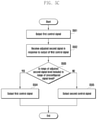
- FIG. 9 is a flowchart illustrating a method for determining a range of a signal level according to an embodiment of the disclosure.
- FIG. 10 is a diagram illustrating an example of a lookup table enumerating ranges of signal levels with regard to respective PVT states according to an embodiment of the disclosure.
- FIG. 11 is a block diagram illustrating a configuration of an electronic device configured to perform a signal level adjustment operation according to various embodiments of the disclosure.
- a main substance of the disclosure may be applied to even other communication systems that have a similar technical background with a little change in a range that is not largely out of the range of the disclosure, and this may be possible by a determination of a person having a skilled technical knowledge in a technical field of the disclosure.
- These computer program instructions may also be stored in a computer usable or computer-readable memory that can direct a computer or other programmable data processing apparatus to function in a particular manner, such that the instructions stored in the computer usable or computer-readable memory produce an article of manufacture including instruction means that implement the function specified in the flowchart block or blocks.
- the computer program instructions may also be loaded onto a computer or other programmable data processing apparatus to cause a series of operation to be performed on the computer or other programmable apparatus to produce a computer implemented process such that the instructions that execute on the computer or other programmable apparatus provide operations for implementing the functions specified in the flowchart block or blocks.
- each block of the flowchart illustrations may represent a module, segment, or portion of code, which includes one or more executable instructions for implementing the specified logical function(s). It should also be noted that in some alternative implementations, the functions noted in the blocks may occur out of the order. For example, two blocks shown in succession may in fact be executed substantially concurrently or the blocks may sometimes be executed in the reverse order, depending upon the functionality involved.
- the “unit” refers to a software element or a hardware element, such as a Field Programmable Gate Array (FPGA) or an Application Specific Integrated Circuit (ASIC), which performs a predetermined function.
- FPGA Field Programmable Gate Array
- ASIC Application Specific Integrated Circuit
- the “unit” does not always have a meaning limited to software or hardware.
- the “unit” may be constructed either to be stored in an addressable storage medium or to execute one or more processors.
- the “unit” includes, for example, software elements, object-oriented software elements, class elements or task elements, processes, functions, properties, procedures, sub-routines, segments of a program code, drivers, firmware, micro-codes, circuits, data, database, data structures, tables, arrays, and parameters.
- the elements and functions provided by the “unit” may be either combined into a smaller number of elements, “unit” or divided into a larger number of elements, “unit”.
- the elements and “units” may be implemented to reproduce one or more central processing units (CPUs) within a device or a security multimedia card.
- CPUs central processing units
- FIG. 1 is a diagram illustrating a schematic structure of a mixer according to an embodiment of the disclosure.
- a mixer is a circuit configured to acquire one output signal from at least two kinds of inputted signals.
- the mixer may perform an operation of applying an inputted second signal to an inputted first signal such that the first signal is converted to a signal in a higher frequency band and then outputted, or converted to a signal in a lower frequency band and then outputted.
- two kinds of signals may be inputted to the mixer 100 .
- a radio frequency (RF) signal and a local oscillator (LO) signal may be inputted to the mixer 100 .
- the LO signal may be applied to another signal inputted to the mixer and thus used to generate an output signal.
- the mixer 100 may apply the LO signal to the RF signal such that the RF signal in a high frequency band is converted to an intermediate frequency (IF) signal in a lower frequency band, and may output the IF signal.
- IF intermediate frequency
- FIG. 1 a mixer 100 is illustrated in FIG. 1 , based on a case in which a wireless signal has been received, such that an RF signal is inputted thereto, and an IF signal is outputted therefrom, the same is applicable to the opposite case in which an IF signal is inputted thereto, and an RF signal is outputted therefrom.
- the mixer applies an LO signal to an inputted signal so as to generate an output signal and, in order to acquire a desired output signal, an ideal LO signal needs to be applied to the input signal.
- the ideal LO signal has the shape of a square wave, but a sine wave having a high amplitude level may be used because, in the case of an actual circuit, the influence of an element such as a gate or capacitance is not negligible.
- an LO signal may undergo an abrupt change in the signal level in various environments. Particularly, when applied to a signal in a high frequency band, the same may change more sensitively to various environments.
- FIG. 2 is a diagram illustrating a process, voltage, and temperature (PVT) state that influences an LO signal according to an embodiment of the disclosure.
- PVT process, voltage, and temperature
- FIGS. 3A, 3B, and 3C are diagrams illustrating a change in LO signal levels according to a PVT state, according to various embodiments of the disclosure.
- the above-mentioned LO signal may be generated by an oscillation unit 210 according to an embodiment, and the oscillation unit 210 may include a local oscillator 211 and a buffer 212 . In addition, the oscillation unit 210 may output the generated LO signal to a mixer, as illustrated in FIG. 2 .
- the local oscillator 211 is configured to generate a local oscillation signal for signal frequency conversion, and the buffer 212 is configured to amplify the local oscillation signal so as to have a voltage value optimized for frequency conversion.
- the local oscillation signal amplified by the buffer 212 is inputted to the mixer as an LO signal, and is applied to convert the frequency of another signal inputted to the mixer.
- the LO signal generated in this manner may undergo an abrupt change in the signal level under various conditions.
- the LO signal may change sensitively to a fabrication process-related change that may occur, to the voltage, and to the temperature.
- PVT factors that may influence the change in the LO signal level
- such an abrupt change in the LO signal level may influence the performance of the mixer that has received the same as an input. It can be confirmed, with reference to FIGS. 3A, 3B, and 3C , to what extent the performance of the mixer will vary as the LO signal level changes according to an embodiment of the disclosure. As the degree of the LO signal level change increases, the amount of current consumed by the mixer will change as illustrated in FIG. 3A , the value of a third order intercept and intermodulation product (IM3) will vary as illustrated in FIG. 3B , or the gain of the mixer will vary as illustrated in FIG. 3C .
- IM3 third order intercept and intermodulation product
- the signal level is adjusted such that a desired signal can be outputted from the mixer.
- FIG. 4 is a diagram illustrating a configuration of an electronic device configured to adjust a signal level according to an embodiment of the disclosure.
- the electronic device may include a mixer 400 , an oscillation unit 410 , and a signal level control unit 420 .
- the mixer 400 may receive at least two kinds of signals as inputs, as described with reference to FIG. 1 , and may generate an output signal by using the same.
- the two kinds of input signals may be an LO signal inputted from the oscillation unit 410 and an RF signal received through wireless communication.
- another signal inputted to the mixer will hereinafter be referred to as a first signal, and the LO signal will be referred to as a second signal.
- the oscillation unit 410 may include a local oscillator 411 and a buffer 412 as described with reference to FIG. 2 , may generate a second signal according to an embodiment, and may output the same to the mixer 400 .
- the electronic device proposed in the disclosure may further include a signal level control unit 420 for adjusting the level of the second signal between the mixer 400 and the oscillation unit 410 , as illustrated in FIG. 4 .
- the signal level control unit 420 may connect the oscillation unit 410 and the mixer 400 on the path of transmission of the second signal from the oscillation unit 410 to the mixer 400 as illustrated in FIG. 4 .
- the signal level control unit 420 according to an embodiment may include a coupler 421 , an envelope detection unit 422 , a signal adjustment unit 423 , and the like.
- the coupler 421 may extract the second signal, which has been outputted toward the mixer 400 from the buffer 412 of the oscillation unit 410 , on the path of transmission of the second signal.
- the second signal extracted by the coupler 421 in this manner may be delivered to the envelope detection unit 422 in order to sense whether or not the level of the second signal changes.
- the envelope detection unit 422 may be connected to the output end of the oscillation unit 410 by the coupler 421 .
- the envelope detection unit 422 may detect an envelope for sensing the signal level range from the second signal delivered from the coupler 421 .
- the envelope detection unit 422 according to the disclosure may convert the detected envelope to an appropriate format more stably through an inverter 424 and an analog-to-digital converter (ADC) 425 , which are connected thereto, and may deliver the same to the signal adjustment unit 423 .
- ADC analog-to-digital converter
- the signal adjustment unit 423 may check the second signal's level range according to the detected envelope. In addition, the signal adjustment unit 423 may compare the checked second signal level range with a preconfigured signal level range and may generate an adjustment signal for adjusting the changed second signal level. The adjustment signal generated by the signal adjustment unit 423 may be inputted to the buffer 412 of the oscillation unit 410 . Generation and output of a control signal according to an embodiment will be described later in more detail with reference to FIG. 5B .
- a digital-to-analog converter (DAC) 426 may be further included between the signal adjustment unit 423 and the buffer 412 of the oscillation unit 410 , as illustrated in FIG. 4 , so as to convert the adjustment signal to bits of a control signal for adjusting the level of the second signal.
- DAC digital-to-analog converter
- the oscillation unit 410 may adjust the level of the second signal based on the control signal. If a third signal is determined by appropriately adjusting the level of the second signal in this manner, the oscillation unit 410 may output the third signal to the mixer 400 . If a signal completely adjusted from the second signal is received from the oscillation unit 410 , the mixer 400 may apply the completely adjusted signal to the already-inputted first signal, thereby generating and outputting the signal to be originally outputted. For convenience of description, the signal completely adjusted from the second signal will hereinafter be referred to as a third signal, and the signal to be originally outputted by the mixer will be referred to as a fourth signal.
- FIG. 4 a process of adjusting the level of a signal according to the first embodiment will be described in detail with reference to FIG. 4 , FIG. 5A , FIG. 5B , and FIG. 5C .
- FIGS. 5A, 5B, and 5C are flowcharts illustrating a method for adjusting a signal level according to various embodiments of the disclosure.
- a first signal may be inputted at operation S 510 .
- the first signal may be a signal inputted to the mixer 400 for frequency band conversion according to an embodiment.
- a second signal for converting the frequency band of the first signal may be outputted at operation S 520 .
- the second signal may be an LO signal generated by the oscillation unit 410 according to an embodiment and outputted to the mixer 400 in order to convert the frequency band of the first signal.
- the outputted second signal may be extracted from the second signal's transmission path at operation S 530 .
- the coupler 421 included in the signal level control unit 420 may extract the outputted second signal from the transmission path between the oscillation unit 410 and the mixer 400 .
- a control signal for adjusting the changed signal level of the second signal may be generated and outputted at operation S 540 .
- a detailed process regarding generation and output of the control signal will now be described with reference to FIG. 5B .
- an envelope may be detected from the extracted second signal at operation S 541 .
- the second signal extracted from the coupler 421 may be delivered to the envelope detection unit 422 such that an envelope for sensing the range of the second signal level may be detected. If the range of the second signal level is checked based on the detected envelope, an adjustment signal for adjusting the changed second signal level may be generated.
- the range of the second signal level based on the detected envelope may be compared with the range of a preconfigured signal level at operation S 542 .
- the signal adjustment unit 423 may check the maximum and minimum values of a second signal magnitude by using the detected envelope, may check the range of the second signal level therefrom, and may confirm whether or not the checked range of the second signal level is included in the range of the preconfigured signal level at operation S 543 .
- a control signal may be outputted such that a third signal for generating a fourth signal is outputted at operation S 544 .
- the signal adjustment unit 423 may confirm that the second signal level has not changed. In this case, the signal adjustment unit 423 may output a control signal for controlling the oscillation unit 410 so as to output a third signal, which has been completely adjusted from the second signal, to the mixer 400 .
- a control signal for adjusting the second signal may be outputted at operation S 545 .
- the signal adjustment unit 423 may generate a control signal such that the range of the changed second signal level is included in the range of the preconfigured signal level.
- the signal adjustment unit 423 may output the generated control signal to the oscillation unit 410 .
- the oscillation unit 410 may receive the control signal and may adjust the second signal by using the same.
- the oscillation unit 410 may determine a third signal completely adjusted from the second signal, based on the control signal received from the signal level control unit 420 , and may output the third signal toward the mixer.
- a fourth signal converted from the first signal may be generated based on the third signal at operation S 550 . That is, if the oscillation unit 410 according to an embodiment outputs a third signal completely adjusted from the second signal to the mixer, the mixer may apply the third signal to the already-inputted first signal, thereby generating a fourth signal that has undergone frequency band conversion from the first signal.
- an embodiment is advantageous in that, even if the LO signal's level is changed by a PVT change, an LO signal suitable for generating the desired output signal can be inputted to the mixer because an element capable of controlling the changed LO signal level is provided on the path of transmission of the LO signal.
- the signal level control unit 420 may confirm whether or not the second signal has been properly adjusted. This is because, if the signal level control unit 420 confirms that the second signal has been properly adjusted, a control signal needs to be generated such that a third signal is outputted from the oscillation unit to the mixer, but if it is determined that the second signal has not been properly adjusted, a control signal for readjusting the adjusted second signal needs to be generated.
- a first control signal for adjusting the second signal may be outputted first at operation S 501 .
- the signal level control unit 420 may output a first signal to the oscillation unit 410 according to an embodiment, and the oscillation unit 410 may adjust the second signal, based on the first control signal.
- the oscillation unit 410 may output the adjusted second signal.
- the adjusted second signal may be received in response to output of the first control signal at operation S 502 .
- the adjusted second signal may be extracted from the coupler 421 included in the signal level control unit 420 according to an embodiment, and may be delivered to the signal adjustment unit 423 . If the adjusted second signal is received, the signal level control unit 420 may determine whether or not the adjusted second signal need to be readjusted.
- the range of the adjusted second signal level is included in the range of a preconfigured signal level at operation S 503 .
- the signal level control unit 420 needs to control the oscillation unit 410 such that the adjusted second signal is outputted from the oscillation unit 410 to the mixer 400 as a third signal.
- the signal level control unit 420 may output a first control signal at operation S 504 , which is identical to the first control signal that has been previously outputted to adjust the second signal, to the oscillation unit 410 such that the adjusted second signal is outputted from the oscillation unit 410 as a third signal.
- the oscillation unit 410 of may determine whether or not the control signal is equal to the previously received control signal. If the same control signal as the previously received first control signal is received, the oscillation unit 410 according to an embodiment may determine the second signal as a third signal, and may output the third signal to the mixer 400 .
- the signal level control unit 420 needs to control the oscillation unit 410 such that the adjusted second signal is readjusted.
- the signal level control unit 420 may generate a second control signal for readjusting the adjusted second signal such that the range of the adjusted second signal level is included in the range of the preconfigured signal level.
- the signal level control unit 420 may output the generated second control signal to the oscillation unit 410 at operation S 505 .
- the oscillation unit 410 may determine whether or not the control signal is equal to the previously received control signal. If a second control signal different from the previously received first control signal is received, the oscillation unit 410 according to an embodiment may readjust the adjusted second signal based on the second control signal. The readjusted second control signal may be again outputted from the oscillation unit 410 .
- an embodiment is advantageous in that, even if an adjusted signal is outputted from the oscillation unit, it is reconfirmed if the adjusted signal has been properly adjusted, and the same is readjusted, thereby making it possible to adjust the abruptly changing LO signal level more precisely and accurately.
- the PVT state not only influences the LO signal level, but also may influence the performance of the mixer.
- a method for adjusting the LO signal level in view of a change in the mixer performance, which follows the PVT state, will be described.
- FIGS. 6A and 6B are diagrams illustrating a PVT state that influences a mixer according to various embodiments of the disclosure.
- FIGS. 7A through 7C are diagrams illustrating a change in the mixer performance according to on the PVT state, according to various embodiments of the disclosure.
- the performance of a mixer 600 according to an embodiment may change depending on a process-related change that may occur, the supplied voltage, and the temperature.
- the mixer 600 according to an embodiment may be configured as illustrated in FIG. 6B , for example.
- the mixer according to an embodiment may be a double balanced active mixer as illustrated in FIG. 6B , for example.
- This is advantageous in that, when processing a signal in a high-frequency band as in a 5G system, leak of the LO signal can be prevented, and loss thereof can be reduced.
- elements included in the mixer such as a switching transistor and the like, may undergo a change in the unique characteristics thereof due to the PVT state.
- the degree of increase in the amount of current consumed by the mixer may be differently derived depending on the process type or temperature.
- FIG. 7B and FIG. 7C different results regarding the IM3 or gain, which depends on a change in the LO signal level, may be derived as the process type and the temperature vary.
- the PVT state not only influences the change in the LO signal level itself, but also changes the characteristics of elements constituting the mixer, and thus may pose a problem of changing the mixer performance. Accordingly, a method capable of adjusting the LO signal level more appropriately by additionally considering a change in the mixer performance, which depends on the PVT state, according to another embodiment will be described.
- FIG. 8 is a diagram illustrating a configuration of an electronic device configured to adjust a signal level according to an embodiment of the disclosure.
- FIG. 9 is a flowchart illustrating a method for determining a range of a signal level according to an embodiment of the disclosure.
- FIG. 10 is a diagram illustrating an example of a lookup table enumerating ranges of signal levels with regard to respective PVT states according to an embodiment of the disclosure. Repeated descriptions of elements identical to those described above will be omitted herein.
- the electronic device may include, in order to adjust a signal level, a mixer 800 , an oscillation unit 810 , and a signal level control unit 820 .
- the signal level control unit 820 may further include a PVT sensing unit 827 capable of sensing a PVT state regarding the mixer 800 .
- the PVT sensing unit 827 may sense the PVT state regarding the mixer and may provide information to the signal adjustment unit 823 such that the changed mixer performance is accordingly reflected in adjustment of the LO signal level.
- the information may refer to information regarding the range of a signal level that serves as a reference used by the signal adjustment unit 823 to confirm whether or not the LO signal level changes. This will be described later in more detail with reference to FIG. 9 and FIG. 10 .
- the PVT sensing unit 827 may further include a PVT sensor 827 a and a state determination unit 827 b .
- the PVT sensor 827 a may include at least one sensor for sensing the PVT state regarding the mixer 800 .
- the PVT sensor 827 a may include a process sensor for sensing a process-related change that may occur, a temperature sensor capable of sensing the temperature of the mixer, a sensor capable of measuring the supplied voltage, and the like.
- the sensed PVT state may be delivered to the state determination unit 827 b .
- the state determination unit 827 b may provide information regarding the range of a reference signal level corresponding to the mixer's performance and state to the signal adjustment unit 823 such that the mixer performance changed according to the PVT state can be used to adjust the LO signal level.
- the PVT state regarding the mixer performance is sensed at operation S 910 , and if the sensed PVT state is delivered, the range of a signal level corresponding to the PVT state regarding the mixer may be determined at operation S 920 .
- the range of the signal level corresponding to the PVT state regarding the mixer may be determined based on a lookup table.
- sensed PVT states may be mapped onto information regarding ranges of signal levels reflecting the mixer performance depending on the same, respectively, thereby constituting a lookup table.
- the state determination unit 827 b may check signal level range information corresponding to a PVT state acquired from the PVT sensor 827 a , based on the lookup table.
- the signal adjustment unit 823 may use the signal level range information received from the state determination unit 827 b in order to confirm whether or not the second signal's level changes.
- a preconfigured signal level range may be determined based on the signal level range information at operation S 930 . If a second signal is extracted from the oscillation unit 810 , the range of the extracted second signal may be compared with the determined signal level range, thereby outputting a control signal for adjusting the second signal.
- the signal adjustment unit 823 may adjust the second signal with reference to the range of the preconfigured first signal level. If the mixer performance has changed due to the PVT state, the PVT sensing unit 827 according to an embodiment may provide information regarding the range of a second signal level reflecting the changed mixer performance to the signal adjustment unit 823 . Thereafter, the signal adjustment unit 823 may change the first signal level range to a second signal level range based on the information provided from the PVT sensing unit 827 , and may use the same to adjust the second signal.
- an embodiment is advantageous in that not only the case in which the LO signal itself is changed by the PVT state, but also a change in the mixer performance can be considered, thereby enabling more precise adjustment of the LO signal level.
- FIG. 11 is a block diagram illustrating a configuration of an electronic device configured to perform a signal level adjustment operation according to various embodiments of the disclosure.
- an electronic device may be any device capable of performing a signal level adjustment operation according to an embodiment.
- the electronic device may include user equipment (UE) capable of transmitting/receiving wireless signals with an external device in a wireless communication system, a mobile station (MS), an eNode B (or base station), a transmitting/receiving device, a radar, and the like.
- UE user equipment
- MS mobile station
- eNode B or base station
- a transmitting/receiving device e.g., a radar, and the like.
- the electronic device may include a transceiver 1110 , a controller 1120 , and a memory 1130 .
- the transceiver 1110 may transmit/receive wireless signals with an external device.
- the transceiver 1110 may include an RF transmitter for up-converting and amplifying the frequency of a signal to be transmitted, an RF receiver for low-noise-amplifying a received signal and down-converting the frequency thereof, and the like.
- the transceiver 1110 may also include a mixer, an oscillation unit, and a signal level control unit for signal level control according to an embodiment.
- the controller 1120 may control a series of processes for operation of the electronic device.
- the controller 1120 may control the transceiver 1110 such that wireless signals are transmitted/received through the transceiver 1110 .
- the memory 1130 may store a default program, an application program, configuration information, data, and the like for operation of the electronic device according to an embodiment.
- the memory 1130 may store a lookup table for determining the range of a signal level according to an embodiment.
Landscapes
- Engineering & Computer Science (AREA)
- Computer Networks & Wireless Communication (AREA)
- Signal Processing (AREA)
- Power Engineering (AREA)
- Superheterodyne Receivers (AREA)
- Transmitters (AREA)
Abstract
Description
Claims (14)
Applications Claiming Priority (2)
| Application Number | Priority Date | Filing Date | Title |
|---|---|---|---|
| KR10-2018-0169147 | 2018-12-26 | ||
| KR1020180169147A KR102733482B1 (en) | 2018-12-26 | 2018-12-26 | Method and apparatus for adjusting a signal level in a wirelss communication system |
Publications (2)
| Publication Number | Publication Date |
|---|---|
| US20200212952A1 US20200212952A1 (en) | 2020-07-02 |
| US11228335B2 true US11228335B2 (en) | 2022-01-18 |
Family
ID=69055675
Family Applications (1)
| Application Number | Title | Priority Date | Filing Date |
|---|---|---|---|
| US16/727,438 Active US11228335B2 (en) | 2018-12-26 | 2019-12-26 | Method and apparatus for adjusting signal level in wireless communication system |
Country Status (4)
| Country | Link |
|---|---|
| US (1) | US11228335B2 (en) |
| EP (1) | EP3675373B1 (en) |
| KR (1) | KR102733482B1 (en) |
| CN (1) | CN111384899B (en) |
Families Citing this family (1)
| Publication number | Priority date | Publication date | Assignee | Title |
|---|---|---|---|---|
| US11601147B2 (en) * | 2020-10-30 | 2023-03-07 | Mediatek Inc. | Semiconductor chip with local oscillator buffer reused for loop-back test and associated loop-back test method |
Citations (25)
| Publication number | Priority date | Publication date | Assignee | Title |
|---|---|---|---|---|
| US5724005A (en) | 1996-04-25 | 1998-03-03 | Lucent Technologies Inc. | Linear power amplifier with automatic gate/base bias control for optimum efficiency |
| EP1350332A2 (en) | 2001-01-12 | 2003-10-08 | QUALCOMM Incorporated | Direct conversion digital domain control |
| US20040048588A1 (en) * | 2002-09-05 | 2004-03-11 | Xytrans, Inc. | MMIC transceiver and low cost subharmonically driven microwave receiver |
| US20060009171A1 (en) * | 2004-07-09 | 2006-01-12 | G-Plus, Inc. | LO leakage and sideband image calibration system and method |
| US7092692B2 (en) * | 2003-03-31 | 2006-08-15 | Agency For Science, Technology And Research | Threshold voltage (Vth), power supply (VDD), and temperature compensation bias circuit for CMOS passive mixer |
| US20070149152A1 (en) * | 2005-12-28 | 2007-06-28 | Bao-Shan Hsiao | Wireless Transmitters with Temperature Gain Compensation |
| US20070243846A1 (en) * | 2006-04-13 | 2007-10-18 | Nec Corporation | Signal processing circuit and signal processing method |
| US20080287076A1 (en) * | 2007-05-17 | 2008-11-20 | Harris Stratex Networks Operating Corporation | Compact Wide Dynamic Range Transmitter For Point To Point Radio |
| US20090174456A1 (en) * | 2006-04-21 | 2009-07-09 | Nec Corporation | DC Offset Correcting Device And DC Offset Correcting Method |
| US20110053547A1 (en) * | 2009-09-01 | 2011-03-03 | Provigent Ltd | Efficient Reduction of Local Oscillator Leakage |
| US20110105060A1 (en) * | 2009-11-04 | 2011-05-05 | Kmw Inc. | Radio frequency transmitter and signal amplification method therefor |
| US20110275341A1 (en) * | 2010-05-10 | 2011-11-10 | Sirf Technology Inc. | Ip2 calibration measurement and signal generation |
| US20120140852A1 (en) * | 2009-08-06 | 2012-06-07 | Akira Kato | Wireless communication apparatus |
| US20130029626A1 (en) * | 2011-07-26 | 2013-01-31 | Mstar Semiconductor, Inc. | Direct Conversion Receiver and Calibration Method Thereof |
| DE102012201990A1 (en) | 2012-02-10 | 2013-08-14 | Robert Bosch Gmbh | Radar sensor with monitoring circuit |
| US20130223488A1 (en) * | 2012-02-27 | 2013-08-29 | Electronics And Telecommunications Research Institute | Apparatus for wideband transmission and reception for multiband |
| US20130259102A1 (en) * | 2012-03-30 | 2013-10-03 | Qualcomm Incorporated | Tunable notch filter using feedback through an existing feedback receiver |
| US8686736B2 (en) | 2010-11-23 | 2014-04-01 | Infineon Technologies Ag | System and method for testing a radio frequency integrated circuit |
| US20140103991A1 (en) | 2012-10-11 | 2014-04-17 | Lsi Corporation | Bounded bias circuit with efficient vt-tracking for high voltage supply/low voltage device |
| US8977211B1 (en) * | 2012-02-29 | 2015-03-10 | Marvell International Ltd. | Systems and methods for calibrating harmonic rejection in switching mixers |
| US9154079B2 (en) | 2012-10-24 | 2015-10-06 | Qualcomm Incorporated | Threshold tracking bias voltage for mixers |
| US20170230920A1 (en) * | 2016-02-04 | 2017-08-10 | Qualcomm Incorporated | Detection of interference in wireless communication devices |
| US20170359029A1 (en) | 2012-12-28 | 2017-12-14 | Peregrine Semiconductor Corporation | Amplifiers Operating in Envelope Tracking Mode or Non-Envelope Tracking Mode |
| US20180159474A1 (en) * | 2016-12-06 | 2018-06-07 | Qualcomm Incorporated | Enhanced broadband operation of an active mixer |
| US10135472B1 (en) * | 2017-08-29 | 2018-11-20 | Analog Devices Global | Apparatus and methods for compensating radio frequency transmitters for local oscillator leakage |
Family Cites Families (3)
| Publication number | Priority date | Publication date | Assignee | Title |
|---|---|---|---|---|
| US6108529A (en) * | 1998-02-01 | 2000-08-22 | Bae Systems Aerospace Electronics Inc. | Radio system including FET mixer device and square-wave drive switching circuit and method therefor |
| US7271668B2 (en) * | 2005-04-14 | 2007-09-18 | Wilinx, Inc. | Mixer circuits and methods with improved spectral purity |
| US9817502B2 (en) * | 2014-12-29 | 2017-11-14 | Synaptics Incorporated | Switched-capacitor harmonic-reject mixer |
-
2018
- 2018-12-26 KR KR1020180169147A patent/KR102733482B1/en active Active
-
2019
- 2019-12-24 EP EP19219682.2A patent/EP3675373B1/en active Active
- 2019-12-25 CN CN201911374224.8A patent/CN111384899B/en active Active
- 2019-12-26 US US16/727,438 patent/US11228335B2/en active Active
Patent Citations (25)
| Publication number | Priority date | Publication date | Assignee | Title |
|---|---|---|---|---|
| US5724005A (en) | 1996-04-25 | 1998-03-03 | Lucent Technologies Inc. | Linear power amplifier with automatic gate/base bias control for optimum efficiency |
| EP1350332A2 (en) | 2001-01-12 | 2003-10-08 | QUALCOMM Incorporated | Direct conversion digital domain control |
| US20040048588A1 (en) * | 2002-09-05 | 2004-03-11 | Xytrans, Inc. | MMIC transceiver and low cost subharmonically driven microwave receiver |
| US7092692B2 (en) * | 2003-03-31 | 2006-08-15 | Agency For Science, Technology And Research | Threshold voltage (Vth), power supply (VDD), and temperature compensation bias circuit for CMOS passive mixer |
| US20060009171A1 (en) * | 2004-07-09 | 2006-01-12 | G-Plus, Inc. | LO leakage and sideband image calibration system and method |
| US20070149152A1 (en) * | 2005-12-28 | 2007-06-28 | Bao-Shan Hsiao | Wireless Transmitters with Temperature Gain Compensation |
| US20070243846A1 (en) * | 2006-04-13 | 2007-10-18 | Nec Corporation | Signal processing circuit and signal processing method |
| US20090174456A1 (en) * | 2006-04-21 | 2009-07-09 | Nec Corporation | DC Offset Correcting Device And DC Offset Correcting Method |
| US20080287076A1 (en) * | 2007-05-17 | 2008-11-20 | Harris Stratex Networks Operating Corporation | Compact Wide Dynamic Range Transmitter For Point To Point Radio |
| US20120140852A1 (en) * | 2009-08-06 | 2012-06-07 | Akira Kato | Wireless communication apparatus |
| US20110053547A1 (en) * | 2009-09-01 | 2011-03-03 | Provigent Ltd | Efficient Reduction of Local Oscillator Leakage |
| US20110105060A1 (en) * | 2009-11-04 | 2011-05-05 | Kmw Inc. | Radio frequency transmitter and signal amplification method therefor |
| US20110275341A1 (en) * | 2010-05-10 | 2011-11-10 | Sirf Technology Inc. | Ip2 calibration measurement and signal generation |
| US8686736B2 (en) | 2010-11-23 | 2014-04-01 | Infineon Technologies Ag | System and method for testing a radio frequency integrated circuit |
| US20130029626A1 (en) * | 2011-07-26 | 2013-01-31 | Mstar Semiconductor, Inc. | Direct Conversion Receiver and Calibration Method Thereof |
| DE102012201990A1 (en) | 2012-02-10 | 2013-08-14 | Robert Bosch Gmbh | Radar sensor with monitoring circuit |
| US20130223488A1 (en) * | 2012-02-27 | 2013-08-29 | Electronics And Telecommunications Research Institute | Apparatus for wideband transmission and reception for multiband |
| US8977211B1 (en) * | 2012-02-29 | 2015-03-10 | Marvell International Ltd. | Systems and methods for calibrating harmonic rejection in switching mixers |
| US20130259102A1 (en) * | 2012-03-30 | 2013-10-03 | Qualcomm Incorporated | Tunable notch filter using feedback through an existing feedback receiver |
| US20140103991A1 (en) | 2012-10-11 | 2014-04-17 | Lsi Corporation | Bounded bias circuit with efficient vt-tracking for high voltage supply/low voltage device |
| US9154079B2 (en) | 2012-10-24 | 2015-10-06 | Qualcomm Incorporated | Threshold tracking bias voltage for mixers |
| US20170359029A1 (en) | 2012-12-28 | 2017-12-14 | Peregrine Semiconductor Corporation | Amplifiers Operating in Envelope Tracking Mode or Non-Envelope Tracking Mode |
| US20170230920A1 (en) * | 2016-02-04 | 2017-08-10 | Qualcomm Incorporated | Detection of interference in wireless communication devices |
| US20180159474A1 (en) * | 2016-12-06 | 2018-06-07 | Qualcomm Incorporated | Enhanced broadband operation of an active mixer |
| US10135472B1 (en) * | 2017-08-29 | 2018-11-20 | Analog Devices Global | Apparatus and methods for compensating radio frequency transmitters for local oscillator leakage |
Non-Patent Citations (3)
| Title |
|---|
| Extended European Search Report dated Apr. 28, 2020, issued in a counterpart European Application No. 19219682.2-1220. |
| Fager et al., "A Comprehensive Analysis of IMD Behavior in RF CMOS Power Amplifier", IEEE Journal of Solid State Circuits, vol. 39, No. 1, Jan. 1, 2004. |
| Kim et al, "Intermodulation analysis of Dual-Gate FET Mixers", IEEE Transactions on Microwave Theory and Techniques, vol. 50, No. 6, Jun. 1, 2002. |
Also Published As
| Publication number | Publication date |
|---|---|
| CN111384899B (en) | 2025-02-28 |
| KR102733482B1 (en) | 2024-11-25 |
| CN111384899A (en) | 2020-07-07 |
| EP3675373B1 (en) | 2022-03-02 |
| EP3675373A1 (en) | 2020-07-01 |
| KR20200079717A (en) | 2020-07-06 |
| US20200212952A1 (en) | 2020-07-02 |
Similar Documents
| Publication | Publication Date | Title |
|---|---|---|
| CN111869277B (en) | Device and method for increasing reference signal power in wireless communication system | |
| KR102807427B1 (en) | Reference signal power boosting in communication systems | |
| US11627535B2 (en) | Emission restricted transmission of reference signals | |
| US11202304B2 (en) | Apparatus and method for transmitting uplink signals in wireless communication system | |
| US12526241B2 (en) | Method and apparatus for quantum computing based resource allocation in wireless communication system | |
| CN112312460B (en) | Method and device for reporting measurement | |
| CN108365877A (en) | A kind of code book feedback method and device | |
| US12009601B2 (en) | Terminal method and device for switching antenna in real-time | |
| CN109983711B (en) | Signal transmission method and device using beamforming in wireless communication system | |
| US12537611B2 (en) | Methods and equipments for locking transmission state | |
| US11283532B2 (en) | Method for testing wireless communication module and electronic device including the wireless communication module | |
| US11228335B2 (en) | Method and apparatus for adjusting signal level in wireless communication system | |
| US11211979B2 (en) | Method and apparatus for controlling transmission power in wireless communication system | |
| CN116195201B (en) | Downlink symbol-level precoding as part of multi-user MISO communication | |
| KR20200011711A (en) | Method and apparatus for i/q calibration | |
| US11528081B2 (en) | Base station and control method therefor in wireless communication system | |
| EP3675381A2 (en) | Electronic device including plurality of antenna arrays | |
| US20240305402A1 (en) | Method and apparatus for performing signal compensation based on frequency resource allocation | |
| US20180351712A1 (en) | Assigning method of pilot signals and base station using the same | |
| US11165403B2 (en) | Antenna module using transmission line length and electronic device including the same | |
| US20260075606A1 (en) | Method and apparatus for selecting modulation scheme in wireless communication system | |
| WO2024168569A1 (en) | Beam pair information reporting | |
| KR20200011803A (en) | Apparatus and method for calibrating phased array antenna |
Legal Events
| Date | Code | Title | Description |
|---|---|---|---|
| AS | Assignment |
Owner name: SAMSUNG ELECTRONICS CO., LTD., KOREA, REPUBLIC OF Free format text: ASSIGNMENT OF ASSIGNORS INTEREST;ASSIGNORS:JANG, JAESIK;AN, KYUHWAN;YOON, YOUNGCHANG;AND OTHERS;SIGNING DATES FROM 20191118 TO 20191119;REEL/FRAME:051370/0214 |
|
| FEPP | Fee payment procedure |
Free format text: ENTITY STATUS SET TO UNDISCOUNTED (ORIGINAL EVENT CODE: BIG.); ENTITY STATUS OF PATENT OWNER: LARGE ENTITY |
|
| STPP | Information on status: patent application and granting procedure in general |
Free format text: DOCKETED NEW CASE - READY FOR EXAMINATION |
|
| STPP | Information on status: patent application and granting procedure in general |
Free format text: FINAL REJECTION MAILED |
|
| STPP | Information on status: patent application and granting procedure in general |
Free format text: RESPONSE AFTER FINAL ACTION FORWARDED TO EXAMINER |
|
| STPP | Information on status: patent application and granting procedure in general |
Free format text: ADVISORY ACTION MAILED |
|
| STPP | Information on status: patent application and granting procedure in general |
Free format text: DOCKETED NEW CASE - READY FOR EXAMINATION |
|
| STPP | Information on status: patent application and granting procedure in general |
Free format text: NON FINAL ACTION MAILED |
|
| STPP | Information on status: patent application and granting procedure in general |
Free format text: RESPONSE TO NON-FINAL OFFICE ACTION ENTERED AND FORWARDED TO EXAMINER |
|
| STPP | Information on status: patent application and granting procedure in general |
Free format text: NOTICE OF ALLOWANCE MAILED -- APPLICATION RECEIVED IN OFFICE OF PUBLICATIONS |
|
| STPP | Information on status: patent application and granting procedure in general |
Free format text: PUBLICATIONS -- ISSUE FEE PAYMENT VERIFIED |
|
| STCF | Information on status: patent grant |
Free format text: PATENTED CASE |
|
| MAFP | Maintenance fee payment |
Free format text: PAYMENT OF MAINTENANCE FEE, 4TH YEAR, LARGE ENTITY (ORIGINAL EVENT CODE: M1551); ENTITY STATUS OF PATENT OWNER: LARGE ENTITY Year of fee payment: 4 |