US11227801B2 - Formation of contacts for semiconductor devices - Google Patents
Formation of contacts for semiconductor devices Download PDFInfo
- Publication number
- US11227801B2 US11227801B2 US16/823,876 US202016823876A US11227801B2 US 11227801 B2 US11227801 B2 US 11227801B2 US 202016823876 A US202016823876 A US 202016823876A US 11227801 B2 US11227801 B2 US 11227801B2
- Authority
- US
- United States
- Prior art keywords
- drain
- source
- top source
- disposed
- fins
- Prior art date
- Legal status (The legal status is an assumption and is not a legal conclusion. Google has not performed a legal analysis and makes no representation as to the accuracy of the status listed.)
- Active
Links
Images


Classifications
-
- H01L21/823418—
-
- H—ELECTRICITY
- H10—SEMICONDUCTOR DEVICES; ELECTRIC SOLID-STATE DEVICES NOT OTHERWISE PROVIDED FOR
- H10D—INORGANIC ELECTRIC SEMICONDUCTOR DEVICES
- H10D84/00—Integrated devices formed in or on semiconductor substrates that comprise only semiconducting layers, e.g. on Si wafers or on GaAs-on-Si wafers
- H10D84/01—Manufacture or treatment
- H10D84/0123—Integrating together multiple components covered by H10D12/00 or H10D30/00, e.g. integrating multiple IGBTs
- H10D84/0126—Integrating together multiple components covered by H10D12/00 or H10D30/00, e.g. integrating multiple IGBTs the components including insulated gates, e.g. IGFETs
- H10D84/013—Manufacturing their source or drain regions, e.g. silicided source or drain regions
-
- H01L21/76229—
-
- H01L21/823468—
-
- H01L21/823475—
-
- H01L29/0653—
-
- H01L29/0847—
-
- H01L29/6656—
-
- H01L29/66666—
-
- H01L29/7827—
-
- H—ELECTRICITY
- H10—SEMICONDUCTOR DEVICES; ELECTRIC SOLID-STATE DEVICES NOT OTHERWISE PROVIDED FOR
- H10D—INORGANIC ELECTRIC SEMICONDUCTOR DEVICES
- H10D30/00—Field-effect transistors [FET]
- H10D30/01—Manufacture or treatment
- H10D30/021—Manufacture or treatment of FETs having insulated gates [IGFET]
- H10D30/025—Manufacture or treatment of FETs having insulated gates [IGFET] of vertical IGFETs
-
- H—ELECTRICITY
- H10—SEMICONDUCTOR DEVICES; ELECTRIC SOLID-STATE DEVICES NOT OTHERWISE PROVIDED FOR
- H10D—INORGANIC ELECTRIC SEMICONDUCTOR DEVICES
- H10D30/00—Field-effect transistors [FET]
- H10D30/60—Insulated-gate field-effect transistors [IGFET]
- H10D30/63—Vertical IGFETs
-
- H—ELECTRICITY
- H10—SEMICONDUCTOR DEVICES; ELECTRIC SOLID-STATE DEVICES NOT OTHERWISE PROVIDED FOR
- H10D—INORGANIC ELECTRIC SEMICONDUCTOR DEVICES
- H10D62/00—Semiconductor bodies, or regions thereof, of devices having potential barriers
- H10D62/10—Shapes, relative sizes or dispositions of the regions of the semiconductor bodies; Shapes of the semiconductor bodies
- H10D62/113—Isolations within a component, i.e. internal isolations
- H10D62/115—Dielectric isolations, e.g. air gaps
- H10D62/116—Dielectric isolations, e.g. air gaps adjoining the input or output regions of field-effect devices, e.g. adjoining source or drain regions
-
- H—ELECTRICITY
- H10—SEMICONDUCTOR DEVICES; ELECTRIC SOLID-STATE DEVICES NOT OTHERWISE PROVIDED FOR
- H10D—INORGANIC ELECTRIC SEMICONDUCTOR DEVICES
- H10D62/00—Semiconductor bodies, or regions thereof, of devices having potential barriers
- H10D62/10—Shapes, relative sizes or dispositions of the regions of the semiconductor bodies; Shapes of the semiconductor bodies
- H10D62/13—Semiconductor regions connected to electrodes carrying current to be rectified, amplified or switched, e.g. source or drain regions
- H10D62/149—Source or drain regions of field-effect devices
- H10D62/151—Source or drain regions of field-effect devices of IGFETs
-
- H—ELECTRICITY
- H10—SEMICONDUCTOR DEVICES; ELECTRIC SOLID-STATE DEVICES NOT OTHERWISE PROVIDED FOR
- H10D—INORGANIC ELECTRIC SEMICONDUCTOR DEVICES
- H10D64/00—Electrodes of devices having potential barriers
- H10D64/01—Manufacture or treatment
- H10D64/021—Manufacture or treatment using multiple gate spacer layers, e.g. bilayered sidewall spacers
-
- H—ELECTRICITY
- H10—SEMICONDUCTOR DEVICES; ELECTRIC SOLID-STATE DEVICES NOT OTHERWISE PROVIDED FOR
- H10D—INORGANIC ELECTRIC SEMICONDUCTOR DEVICES
- H10D64/00—Electrodes of devices having potential barriers
- H10D64/20—Electrodes characterised by their shapes, relative sizes or dispositions
- H10D64/23—Electrodes carrying the current to be rectified, amplified, oscillated or switched, e.g. sources, drains, anodes or cathodes
- H10D64/251—Source or drain electrodes for field-effect devices
- H10D64/252—Source or drain electrodes for field-effect devices for vertical or pseudo-vertical devices
-
- H—ELECTRICITY
- H10—SEMICONDUCTOR DEVICES; ELECTRIC SOLID-STATE DEVICES NOT OTHERWISE PROVIDED FOR
- H10D—INORGANIC ELECTRIC SEMICONDUCTOR DEVICES
- H10D84/00—Integrated devices formed in or on semiconductor substrates that comprise only semiconducting layers, e.g. on Si wafers or on GaAs-on-Si wafers
- H10D84/01—Manufacture or treatment
- H10D84/0123—Integrating together multiple components covered by H10D12/00 or H10D30/00, e.g. integrating multiple IGBTs
- H10D84/0126—Integrating together multiple components covered by H10D12/00 or H10D30/00, e.g. integrating multiple IGBTs the components including insulated gates, e.g. IGFETs
- H10D84/0147—Manufacturing their gate sidewall spacers
-
- H—ELECTRICITY
- H10—SEMICONDUCTOR DEVICES; ELECTRIC SOLID-STATE DEVICES NOT OTHERWISE PROVIDED FOR
- H10D—INORGANIC ELECTRIC SEMICONDUCTOR DEVICES
- H10D84/00—Integrated devices formed in or on semiconductor substrates that comprise only semiconducting layers, e.g. on Si wafers or on GaAs-on-Si wafers
- H10D84/01—Manufacture or treatment
- H10D84/0123—Integrating together multiple components covered by H10D12/00 or H10D30/00, e.g. integrating multiple IGBTs
- H10D84/0126—Integrating together multiple components covered by H10D12/00 or H10D30/00, e.g. integrating multiple IGBTs the components including insulated gates, e.g. IGFETs
- H10D84/0149—Manufacturing their interconnections or electrodes, e.g. source or drain electrodes
-
- H—ELECTRICITY
- H10—SEMICONDUCTOR DEVICES; ELECTRIC SOLID-STATE DEVICES NOT OTHERWISE PROVIDED FOR
- H10D—INORGANIC ELECTRIC SEMICONDUCTOR DEVICES
- H10D84/00—Integrated devices formed in or on semiconductor substrates that comprise only semiconducting layers, e.g. on Si wafers or on GaAs-on-Si wafers
- H10D84/01—Manufacture or treatment
- H10D84/0123—Integrating together multiple components covered by H10D12/00 or H10D30/00, e.g. integrating multiple IGBTs
- H10D84/0126—Integrating together multiple components covered by H10D12/00 or H10D30/00, e.g. integrating multiple IGBTs the components including insulated gates, e.g. IGFETs
- H10D84/016—Integrating together multiple components covered by H10D12/00 or H10D30/00, e.g. integrating multiple IGBTs the components including insulated gates, e.g. IGFETs the components including vertical IGFETs
-
- H—ELECTRICITY
- H10—SEMICONDUCTOR DEVICES; ELECTRIC SOLID-STATE DEVICES NOT OTHERWISE PROVIDED FOR
- H10D—INORGANIC ELECTRIC SEMICONDUCTOR DEVICES
- H10D84/00—Integrated devices formed in or on semiconductor substrates that comprise only semiconducting layers, e.g. on Si wafers or on GaAs-on-Si wafers
- H10D84/01—Manufacture or treatment
- H10D84/02—Manufacture or treatment characterised by using material-based technologies
- H10D84/03—Manufacture or treatment characterised by using material-based technologies using Group IV technology, e.g. silicon technology or silicon-carbide [SiC] technology
- H10D84/038—Manufacture or treatment characterised by using material-based technologies using Group IV technology, e.g. silicon technology or silicon-carbide [SiC] technology using silicon technology, e.g. SiGe
-
- H—ELECTRICITY
- H10—SEMICONDUCTOR DEVICES; ELECTRIC SOLID-STATE DEVICES NOT OTHERWISE PROVIDED FOR
- H10W—GENERIC PACKAGES, INTERCONNECTIONS, CONNECTORS OR OTHER CONSTRUCTIONAL DETAILS OF DEVICES COVERED BY CLASS H10
- H10W10/00—Isolation regions in semiconductor bodies between components of integrated devices
- H10W10/01—Manufacture or treatment
- H10W10/011—Manufacture or treatment of isolation regions comprising dielectric materials
- H10W10/014—Manufacture or treatment of isolation regions comprising dielectric materials using trench refilling with dielectric materials, e.g. shallow trench isolations
- H10W10/0143—Manufacture or treatment of isolation regions comprising dielectric materials using trench refilling with dielectric materials, e.g. shallow trench isolations comprising concurrently refilling multiple trenches having different shapes or dimensions
-
- H—ELECTRICITY
- H10—SEMICONDUCTOR DEVICES; ELECTRIC SOLID-STATE DEVICES NOT OTHERWISE PROVIDED FOR
- H10W—GENERIC PACKAGES, INTERCONNECTIONS, CONNECTORS OR OTHER CONSTRUCTIONAL DETAILS OF DEVICES COVERED BY CLASS H10
- H10W10/00—Isolation regions in semiconductor bodies between components of integrated devices
- H10W10/10—Isolation regions comprising dielectric materials
- H10W10/17—Isolation regions comprising dielectric materials formed using trench refilling with dielectric materials, e.g. shallow trench isolations
-
- H—ELECTRICITY
- H10—SEMICONDUCTOR DEVICES; ELECTRIC SOLID-STATE DEVICES NOT OTHERWISE PROVIDED FOR
- H10D—INORGANIC ELECTRIC SEMICONDUCTOR DEVICES
- H10D30/00—Field-effect transistors [FET]
- H10D30/60—Insulated-gate field-effect transistors [IGFET]
- H10D30/67—Thin-film transistors [TFT]
- H10D30/6728—Vertical TFTs
-
- H—ELECTRICITY
- H10—SEMICONDUCTOR DEVICES; ELECTRIC SOLID-STATE DEVICES NOT OTHERWISE PROVIDED FOR
- H10D—INORGANIC ELECTRIC SEMICONDUCTOR DEVICES
- H10D84/00—Integrated devices formed in or on semiconductor substrates that comprise only semiconducting layers, e.g. on Si wafers or on GaAs-on-Si wafers
- H10D84/80—Integrated devices formed in or on semiconductor substrates that comprise only semiconducting layers, e.g. on Si wafers or on GaAs-on-Si wafers characterised by the integration of at least one component covered by groups H10D12/00 or H10D30/00, e.g. integration of IGFETs
- H10D84/82—Integrated devices formed in or on semiconductor substrates that comprise only semiconducting layers, e.g. on Si wafers or on GaAs-on-Si wafers characterised by the integration of at least one component covered by groups H10D12/00 or H10D30/00, e.g. integration of IGFETs of only field-effect components
- H10D84/83—Integrated devices formed in or on semiconductor substrates that comprise only semiconducting layers, e.g. on Si wafers or on GaAs-on-Si wafers characterised by the integration of at least one component covered by groups H10D12/00 or H10D30/00, e.g. integration of IGFETs of only field-effect components of only insulated-gate FETs [IGFET]
Definitions
- the present invention generally relates to semiconductor devices, and more particularly to the formation of contacts for semiconductor devices.
- CMOS complementary metal-oxide semiconductor
- a method for fabricating a semiconductor device includes forming top source/drain contact material on top source/drain material disposed on one or more fins of a base structure, and subtractively patterning the top source/drain contact material to form at least one top source/drain contact.
- the at least one top source/drain contact has a positive tapered geometry.
- the method further includes cutting exposed end portions of the top source/drain material to form at least one top source/drain region underneath the at least one top source/drain contact.
- a method for fabricating a semiconductor device includes forming top source/drain material merged across at least a first fin and a second fin disposed on a bottom source/drain region of a base structure, forming top source/drain contact material on the top source/drain material, and subtractively patterning the top source/drain contact material to form at least a first top source/drain contact.
- the at least one top source/drain contact having a positive tapered geometry.
- the method further includes cutting exposed end portions of the top source/drain material to form a plurality of top source/drain regions including at least merged first and second top source/drain regions underneath the at least one top source/drain contact.
- the first top source/drain contact is formed on the merged first and second top source/drain regions.
- a semiconductor device in accordance with yet another embodiment of the present invention, includes a substrate a bottom source/drain region disposed on the substrate, one or more fins disposed on the bottom source/drain region, one or more top source drain/regions disposed on respective ones of the one or more fins, one or more gate structures adjacent to the one or more fins, at least one bottom source/drain contact and at least one gate contact each having a negative tapered geometry, and at least one top source/drain contact having a positive tapered geometry.
- FIG. 1 is a cross-sectional view of a base structure formed on a substrate during the fabrication of a semiconductor device, in accordance with an embodiment of the present invention
- FIG. 2 is another cross-sectional view of the semiconductor device of FIG. 1 , in accordance with an embodiment of the present invention
- FIG. 3 is a cross-sectional view of the formation of top source/drain regions, contact material and patterning masks during the fabrication of the semiconductor device, in accordance with an embodiment of the present invention
- FIG. 4 is another cross-sectional view of the semiconductor device of FIG. 3 , in accordance with an embodiment of the present invention.
- FIG. 5 is a cross-sectional view of patterning of the contact material using a subtractive patterning process and a cut of exposed end portions of the top source/drain regions after the patterning during the fabrication of the semiconductor device, in accordance with an embodiment of the present invention
- FIG. 6 is a cross-sectional view of the removal of the patterning masks and the formation of an ILD layer during the fabrication of the semiconductor device, in accordance with an embodiment of the present invention
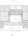
- FIG. 7 is another cross-sectional view of the semiconductor device of FIG. 6 , in accordance with an embodiment of the present invention.
- FIG. 8 is a cross-sectional view of the formation a bottom source/drain contact and a gate contact during the fabrication of the semiconductor device, in accordance with an embodiment of the present invention.
- FIG. 9 is a cross-sectional view of the formation a bottom source/drain contact and a gate contact during the fabrication of the semiconductor device, in accordance with another embodiment of the present invention.
- FIG. 10 is a block/flow diagram illustrating a system/method for fabricating a semiconductor device, in accordance with an embodiment of the present invention.
- the embodiments described herein provide for the formation of a semiconductor device having contacts that reduce risk of device shorts. More specifically, the embodiments described herein can provide for the formation of semiconductor device including a vertical transistor device (e.g., a VTFET) having a top source/drain contact with a positive tapered geometry (e.g., positive tapered profile), and a bottom source/drain contact and gate contact with negative tapered geometries (e.g., negative tapered profiles).
- a vertical transistor device e.g., a VTFET
- top source/drain regions disposed on respective fins underneath the same top source/drain contact can be merged.
- top source/drain contact material can be formed on a top source/drain region, which can be a merged top source/drain region shared by at least two semiconductor fins.
- At least one top source/drain contact can be formed by patterning the top source/drain contact material using a subtractive patterning process, and end portions of the top source/drain contact material exposed by the subtractive patterning can be cut to isolate the vertical transistor device.
- At least one bottom source/drain contact and at least one gate contact can be formed using a damascene trench process, where conductive material is formed within a trench.
- the top source/drain contact can have a positive tapered geometry due to the subtractive patterning process, whereas the bottom source/drain contact and the gate contact can have negative tapered geometry due to the damascene trench process.
- the vertical transistor device can further include a barrier liner disposed along a bottom surface of the at least one top source/drain contact (and not on the sidewalls of the top source/drain contact).
- the barrier line can be further formed along bottom surfaces and sidewalls of the at least one bottom source/drain contact and the at least one gate contact.
- the at least one top source/drain region can be self-aligned to the at least one top source/drain contact, and can have an abrupt shape, as a result of cutting the top source/drain epitaxial material using the top source/drain contact as a mask.
- the present embodiments can include a design for an integrated circuit chip, which can be created in a graphical computer programming language, and stored in a computer storage medium (such as a disk, tape, physical hard drive, or virtual hard drive such as in a storage access network). If the designer does not fabricate chips or the photolithographic masks used to fabricate chips, the designer can transmit the resulting design by physical means (e.g., by providing a copy of the storage medium storing the design) or electronically (e.g., through the Internet) to such entities, directly or indirectly.
- the stored design is then converted into the appropriate format (e.g., GDSII) for the fabrication of photolithographic masks, which typically include multiple copies of the chip design in question that are to be formed on a wafer.
- the photolithographic masks are utilized to define areas of the wafer (and/or the layers thereon) to be etched or otherwise processed.
- the resulting integrated circuit chips can be distributed by the fabricator in raw wafer form (that is, as a single wafer that has multiple unpackaged chips), as a bare die, or in a packaged form.
- the chip is mounted in a single chip package (such as a plastic carrier, with leads that are affixed to a motherboard or other higher-level carrier) or in a multichip package (such as a ceramic carrier that has either or both surface interconnections or buried interconnections).
- the chip is then integrated with other chips, discrete circuit elements, and/or other signal processing devices as part of either (a) an intermediate product, such as a motherboard, or (b) an end product.
- the end product can be any product that includes integrated circuit chips, ranging from toys and other low-end applications to advanced computer products having a display, a keyboard or other input device, and a central processor.
- material compounds will be described in terms of listed elements, e.g., SiGe. These compounds include different proportions of the elements within the compound, e.g., SiGe includes Si x Ge 1-x where x is less than or equal to 1, etc.
- SiGe includes Si x Ge 1-x where x is less than or equal to 1, etc.
- other elements can be included in the compound and still function in accordance with the present principles.
- the compounds with additional elements will be referred to herein as alloys.
- any of the following “/”, “and/or”, and “at least one of”, for example, in the cases of “A/B”, “A and/or B” and “at least one of A and B”, is intended to encompass the selection of the first listed option (A) only, or the selection of the second listed option (B) only, or the selection of both options (A and B).
- such phrasing is intended to encompass the selection of the first listed option (A) only, or the selection of the second listed option (B) only, or the selection of the third listed option (C) only, or the selection of the first and the second listed options (A and B) only, or the selection of the first and third listed options (A and C) only, or the selection of the second and third listed options (B and C) only, or the selection of all three options (A and B and C).
- This can be extended, as readily apparent by one of ordinary skill in this and related arts, for as many items listed.
- spatially relative terms such as “beneath,” “below,” “lower,” “above,” “upper,” and the like, can be used herein for ease of description to describe one element's or feature's relationship to another element(s) or feature(s) as illustrated in the FIGS. It will be understood that the spatially relative terms are intended to encompass different orientations of the device in use or operation in addition to the orientation depicted in the FIGS. For example, if the device in the FIGS. is turned over, elements described as “below” or “beneath” other elements or features would then be oriented “above” the other elements or features. Thus, the term “below” can encompass both an orientation of above and below.
- the device can be otherwise oriented (rotated 90 degrees or at other orientations), and the spatially relative descriptors used herein can be interpreted accordingly.
- a layer is referred to as being “between” two layers, it can be the only layer between the two layers, or one or more intervening layers can also be present.
- FIG. 1 shows a cross-sectional view of the device 100 across a fin cut
- FIG. 2 shows a cross-sectional view of the device 100 along the fin cut.
- the substrate 102 can include any suitable substrate structure, e.g., a bulk semiconductor, a semiconductor-on-insulator (SOI) substrate, etc.
- the substrate 102 can include a silicon-containing material.
- Si-containing materials suitable for the substrate 102 can include, but are not limited to, Si, SiGe, SiGeC, SiC and multi-layers thereof.
- silicon is the predominantly used semiconductor material in wafer fabrication, alternative semiconductor materials can be employed as additional layers, such as, but not limited to, germanium, gallium arsenide.
- a bottom source/drain region 104 is formed on the substrate 102 , and shallow trench isolation (STI) regions 106 are formed on the substrate to a height of the bottom source/drain region 104 .
- the bottom source/drain region 104 and the STI regions 106 can include any suitable materials in accordance with the embodiments described herein.
- the bottom source/drain region 104 can include epitaxially material that is epitaxially grown or deposited on the substrate 102 .
- the STI regions 106 can include, e.g., silicon dioxide (SiO 2 ) or other suitable dielectric material.
- epitaxial growth and/or deposition means the growth of a semiconductor material on a deposition surface of a semiconductor material, in which the semiconductor material being grown has substantially the same crystalline characteristics as the semiconductor material of the deposition surface.
- epitaxial material denotes a material that is formed using epitaxial growth.
- the depositing atoms arrive at the deposition surface with sufficient energy to move around on the surface and orient themselves to the crystal arrangement of the atoms of the deposition surface.
- an epitaxial film deposited on a ⁇ 100 ⁇ crystal surface will take on a ⁇ 100 ⁇ orientation.
- a plurality of semiconductor fins including fins 108 - 1 through 108 - 3 are formed on the bottom source/drain region 104 . That is, in this embodiment, the fins 108 - 1 through 108 - 3 share a common bottom source/drain region.
- the plurality of fins can include any suitable material in accordance with the embodiments described herein.
- the plurality of fins can include, e.g., Si, Ge, SiGe, or other suitable semiconductor material.
- a bottom spacer 110 is formed on the bottom source/drain region 104 and STI regions 106 adjacent to the fins 108 - 1 through 108 - 3 .
- the bottom spacer 110 can include any suitable dielectric material in accordance with the embodiments described herein. Examples of materials that can be used to form the bottom spacer 110 include, but are not limited to, SiO 2 , silicon nitride (SiN), etc.
- gate structures 112 are formed on the bottom spacer 110 and along the sidewalls of the fins 108 - 1 through 108 - 3 .
- the gate structures 112 can include any suitable materials in accordance with the embodiments described herein. More specifically, the gate structures 112 can include a gate dielectric and a gate conductor.
- the gate structures 112 can include high-k metal gate (HKMG) materials.
- HKMG material includes a high-k dielectric material as the gate dielectric and a metal gate as the gate conductor (as opposed to a polysilicon gate).
- a high-k dielectric material is one that has a dielectric constant k greater than the dielectric constant of SiO 2 at room temperature (e.g., about 20° C.-25° C.) and atmospheric pressure (e.g., about 1 atm).
- a high-k dielectric material can have a dielectric constant of greater than about 3.9.
- high-k dielectric materials examples include, but are not limited to, hafnium silicate (HfO 4 Si), zirconium silicate (ZrSiO 4 ), hafnium dioxide (HfO 2 ) and zirconium dioxide (ZrO 2 ).
- interlevel dielectric (ILD) layers 114 are formed on the bottom spacer 110 providing insulation between the gate structures 112 .
- the ILD layers 114 can include any suitable dielectric material in accordance with the embodiments described herein.
- the ILD layers 114 can include, e.g., SiO 2 or other suitable dielectric material.
- pairs of top spacers 116 are each formed on a gate structure 112 adjacent to one of the fins 108 - 1 through 108 - 3 .
- the top spacers 116 can include any suitable dielectric material in accordance with the embodiments described herein. Examples of materials that can be used to form the bottom spacer 110 include, but are not limited to, SiO 2 , silicon nitride (SiN), etc.
- top source/drain region material 118 is formed on the fins 108 - 1 through 108 - 3 extending above the ILD layers 114 and the top spacers 116 .
- the top source/drain region material 118 can purposely be formed to be merged.
- the top source/drain region material 118 can include any suitable material in accordance with the embodiments described herein.
- the top source/drain region material 118 can include an epitaxially grown material.
- top source/drain contact material 120 is formed on the top source/drain region material 118 .
- the top source/drain contact material 120 can be formed as wrap around contact material.
- the top source/drain contact material 120 can include any suitable material in accordance with the embodiments described herein. Examples of materials that can be used to form the top source/drain contact material 120 include, but are not limited to, copper (Cu), cobalt (Co), tantalum (Ta), ruthenium (Ru), titanium (Ti), and/or other suitable conductive materials or metals.
- the top source/drain contact material 120 includes a metal silicide.
- the top source/drain contact material 120 can include, e.g., a Ti-based silicide.
- patterning material 122 separated by gaps 124 - 1 through 124 - 3 are formed on the top source/drain contact material 120 .
- a subtractive patterning process will be used to pattern top source/drain contacts from the top source/drain contact material 120 , and the top source/drain region material 118 will be cut to form top source/drain regions.
- the patterning material 122 can include any suitable material in accordance with the embodiments described herein. Examples of materials that can be used to form the patterning material 122 include, but are not limited to, hardmask material and/or organic planarization layers (OPLs).
- the cross-sectional view of the device 100 across the fin cut is provided showing the patterning of the top source/drain contact material 120 using a subtractive patterning process to form a first set of cavities 126 - 1 and 126 - 2 and top source/drain contacts 128 - 1 and 128 - 2 .
- Any suitable subtractive patterning process can be used to pattern the top source/drain contact material 120 in accordance with the embodiments described herein.
- a subtractive reactive-ion etch (RIE) process can be used to pattern the top source/drain contact material 120 to form the top source/drain contacts 128 - 1 and 128 - 2 .
- RIE reactive-ion etch
- top source/drain contact material 120 is patterned, exposed end portions of the top source/drain region material 118 are cut to form a second set of cavities 130 - 1 through 130 - 3 and top source/drain regions 132 - 1 through 130 - 3 . Any suitable process can be used to cut the exposed end portions of the top source/drain region material 118 in accordance with the embodiments described herein.
- the top source/drain contact 128 - 1 in this embodiment is shared between the top source/drain regions 132 - 1 and 132 - 2 , which are merged, while the top source/drain contact 128 - 2 is disposed on the single top source/drain region 132 - 3 .
- the top source/drain contacts 128 - 1 and 128 - 2 each have a positive tapered geometry (e.g., positive tapered profile) as a result of the subtractive patterning process.
- the patterning material 122 is removed, and ILD layers 134 are formed within the first and second sets of cavities 126 - 1 , 126 - 2 and 130 - 1 through 130 - 3 .
- the patterning material 112 can be removed and the ILD layers 134 can be formed using any suitable processes in accordance with the embodiments described herein.
- the ILD layers 134 can be formed by depositing dielectric material and planarizing the dielectric material to form the ILD layers 134 (e.g., using chemical-mechanical planarization (CMP)).
- CMP chemical-mechanical planarization
- the ILD layers 134 can include any suitable material in accordance with the embodiments described herein (e.g., SiO 2 ).
- the cross-sectional view of the device 100 along the fin cut is provided showing the formation of at least one bottom source/drain contact 136 on the bottom source/drain region 104 , and at least one gate contact 138 on the gate structure 112 . More specifically, openings corresponding to the contacts 136 and 138 can be patterned using an etch process, and conductive material can be formed within the openings to form the contacts 136 and 138 .
- the bottom source/drain contact 136 and the gate contact 138 each have a positive tapered geometry (e.g., positive tapered profile) as a result of the damascene trench process used to form the bottom source/drain contact 136 and the gate contact 138 .
- the contacts 136 and 138 can include any suitable material in accordance with the embodiments described herein. Examples of materials that can be used to form the contacts 136 and 138 include, but are not limited to, copper (Cu), cobalt (Co), tantalum (Ta), ruthenium (Ru), titanium (Ti), and/or other suitable conductive materials or metals.
- the contacts 136 and 138 can include, e.g., a metal silicide (e.g., a Ti-based silicide).
- the contacts 128 - 1 , 128 - 2 , 136 and 138 include the same or similar material. In other embodiments, one or more of the contacts 128 - 1 , 128 - 2 , 136 and 138 can include a different material.
- FIG. 9 a cross-sectional view of a device 200 along a fin cut is provided.
- the device 200 is similar to the device 100 shown in FIG. 8 , except that a barrier liner 202 is along the bottom surface of the top source/drain contact 128 - 1 , and barrier liners 204 and 206 are along sidewalls and the bottom surfaces of the contacts 136 and 138 , respectively. There is a lack of the barrier liner 202 along the sidewalls of the top source/drain contact 128 - 1 due to the subtractive patterning process used to form the top source/drain contact 128 - 1 .
- the barrier liners 202 through 206 can include any suitable materials in accordance with the embodiments described herein. Examples of materials that can be used to form the barrier liners 202 - 1 through 202 - 3 include, but are not limited to, tantalum (Ta), titanium (Ti), tungsten W, tantalum nitride (TaN), titanium nitride (TiN), tungsten nitride (WN), doped or undoped silicon carbide (e.g., SiC), doped or undoped silicon nitride (e.g., SiN), etc. In one embodiment, the barrier liners 202 through 206 include a same material. In another embodiment, at least one of the barrier liners 202 through 206 include a different material.
- a block/flow diagram is provided illustrating a system/method 300 for fabricating a semiconductor device.
- a base structure of a vertical transistor device is formed on a substrate, with the base structure including a bottom source/drain region, one or more fins, one or more gate structures and one or more first interlevel dielectric (ILD) layers.
- the one or more fins are disposed on the bottom source/drain region, and the one or more gate structures are formed adjacent to each of the one or more fins.
- the one or more fins can include at least first and second fins.
- the base structure can further include at least one shallow trench isolation (STI) region disposed on the substrate to a height of the bottom source/drain region, a bottom spacer disposed on the bottom source/drain region and the at least one STI region adjacent to the one or more fins, one or more pairs of top spacers disposed on respective ones of the one or more gate structures adjacent to the one or more fins.
- the one or more first ILD layers are disposed on the bottom spacer between the one or more gate structures and the one or more pairs of top spacers to a height of the one or more pairs of top spacers.
- the substrate and base structure components can include any suitable materials in accordance with the embodiments described herein.
- the substrate can include any suitable substrate structure, e.g., a bulk semiconductor, a semiconductor-on-insulator (SOI) substrate, etc.
- the substrate can include a silicon-containing material.
- Si-containing materials suitable for the substrate can include, but are not limited to, Si, SiGe, SiGeC, SiC and multi-layers thereof.
- silicon is the predominantly used semiconductor material in wafer fabrication, alternative semiconductor materials can be employed as additional layers, such as, but not limited to, germanium, gallium arsenide.
- the bottom source/drain region can including epitaxial material epitaxially grown or deposited on the substrate.
- the one or more fins can include, e.g., Si, Ge, SiGe, or other suitable semiconductor material.
- the one or more gate structures can include a gate dielectric and a gate conductor.
- the one or more gate structures can include high-k metal gate (HKMG) materials.
- the STI regions can include, e.g., silicon dioxide (SiO 2 ) or other suitable dielectric material.
- Examples of materials that can be used to form the bottom spacer include, but are not limited to, SiO 2 , silicon nitride (SiN), etc.
- the one or more first ILD layers can include, e.g., SiO 2 or other suitable dielectric material.
- block 302 Further details regarding block 302 are described above with reference to FIGS. 1-2 .
- top source/drain material is formed on the one or more fins.
- the top source/drain material can be formed to be merged across the first and second fins.
- the one or more fins can further include a third fin, and the top source/drain material can be formed to be merged across the first, second and third fins.
- the top source/drain region material can include any suitable material in accordance with the embodiments described herein.
- the top source/drain region material can include an epitaxially grown material.
- top source/drain contact material is formed on the top source/drain material.
- the top source/drain contact material can be formed as wrap around contact material.
- the top source/drain contact material can include any suitable material in accordance with the embodiments described herein. Examples of materials that can be used to form the top source/drain contact material include, but are not limited to, copper (Cu), cobalt (Co), tantalum (Ta), ruthenium (Ru), titanium (Ti), and/or other suitable conductive materials or metals.
- the top source/drain contact material includes a metal silicide.
- the top source/drain contact material can include, e.g., a Ti-based silicide.
- the top source/drain contact material is subtractively patterned to form at least one top source/drain contact. More specifically, subtractively patterning the top source/drain contact material to form the at least one top source/drain contact can include forming patterning material, and etching through gaps between the pattern material up to the top source/drain material. The subtractive patterning further results in the formation of a first set of cavities. Any suitable process can be used to subtractively pattern the top source/drain contact material in accordance with the embodiments described herein. For example, a reactive-ion etch (RIE) process can be used. The subtractive patterning results in the at least one top source/drain contact having a positive tapered geometry.
- RIE reactive-ion etch
- exposed end portions of the top source/drain material are cut to form at least one top source/drain region underneath the at least one top source/drain contact.
- the cutting further results in the formation of a second set of cavities underneath the first set of cavities. Any suitable process can be used to cut the exposed end portions of the top source/drain region material to form the top source/drain regions in accordance with the embodiments described herein.
- the at least one top source/drain region includes merged first and second top source/drain regions disposed on the first and second fins
- the at least one top source/drain contact includes at least a first top source/drain contact disposed on the merged first and second top source/drain regions.
- the one or more fins further include a third fin
- a third top source/drain region disconnected from the merged first and second source/drain regions can be disposed on the third fin
- the at least one top source/drain contact further includes a second top source/drain contact disposed on the third source/drain region.
- a first barrier liner can be formed on the top source/drain material prior to formation of the at least one top source/drain contact. There is a lack of the first barrier liner along the sidewalls of the at least one top source/drain contact due to the subtractive patterning process used to form the at least one top source/drain contact.
- first barrier liner examples include, but are not limited to, tantalum (Ta), titanium (Ti), tungsten W, tantalum nitride (TaN), titanium nitride (TiN), tungsten nitride (WN), doped or undoped silicon carbide (e.g., SiC), doped or undoped silicon nitride (e.g., SiN), etc.
- blocks 304 - 310 are described above with reference to FIGS. 3-5 and 9 .
- one or more second ILD layers are formed on the one or more first ILD layers. More specifically, the one or more second ILD layers are formed within the first and second sets of cavities.
- the one or more second ILD layers can be formed by depositing dielectric material and planarizing the dielectric material to form the ILD layers (e.g., using chemical-mechanical planarization (CMP)).
- CMP chemical-mechanical planarization
- the one or more second ILD layers can include any suitable material in accordance with the embodiments described herein (e.g., SiO 2 ).
- a plurality of contacts including at least one bottom source/drain contact on the bottom source/drain region and at least one gate contact on the one or more gate structures are formed. More specifically, forming the plurality of contacts can include forming a plurality of openings corresponding to the plurality of contacts using an etch process, and forming conductive material within the plurality of openings.
- the plurality of contacts can include any suitable material in accordance with the embodiments described herein.
- materials that can be used to form the plurality of contacts include, but are not limited to, copper (Cu), cobalt (Co), tantalum (Ta), ruthenium (Ru), titanium (Ti), and/or other suitable conductive materials or metals.
- the plurality of contacts can include, e.g., a metal silicide (e.g., a Ti-based silicide).
- the formation of the plurality of contacts result in the plurality of contacts having a negative tapered geometry.
- the at least one top source/drain contact, the at least one bottom source/drain contact and the at least one gate contact include the same or similar material. In other embodiments, these contacts can include a different material.
- forming the at least one bottom source/drain contact and the at least one gate contact can further include forming a second barrier liner and a third barrier liner along sidewalls and the bottom surfaces of the at least one bottom source/drain contact and the at least one gate contact, respectively.
- materials that can be used to form the second and third barrier liners include, but are not limited to, tantalum (Ta), titanium (Ti), tungsten W, tantalum nitride (TaN), titanium nitride (TiN), tungsten nitride (WN), doped or undoped silicon carbide (e.g., SiC), doped or undoped silicon nitride (e.g., SiN), etc.
- first, second and third barrier liners include the same material. In other embodiments, at least one of the first, second and third barrier liners can include a different material.
Landscapes
- Insulated Gate Type Field-Effect Transistor (AREA)
- Thin Film Transistor (AREA)
- Electrodes Of Semiconductors (AREA)
Abstract
Description
Claims (20)
Priority Applications (1)
| Application Number | Priority Date | Filing Date | Title |
|---|---|---|---|
| US16/823,876 US11227801B2 (en) | 2020-03-19 | 2020-03-19 | Formation of contacts for semiconductor devices |
Applications Claiming Priority (1)
| Application Number | Priority Date | Filing Date | Title |
|---|---|---|---|
| US16/823,876 US11227801B2 (en) | 2020-03-19 | 2020-03-19 | Formation of contacts for semiconductor devices |
Publications (2)
| Publication Number | Publication Date |
|---|---|
| US20210296178A1 US20210296178A1 (en) | 2021-09-23 |
| US11227801B2 true US11227801B2 (en) | 2022-01-18 |
Family
ID=77748643
Family Applications (1)
| Application Number | Title | Priority Date | Filing Date |
|---|---|---|---|
| US16/823,876 Active US11227801B2 (en) | 2020-03-19 | 2020-03-19 | Formation of contacts for semiconductor devices |
Country Status (1)
| Country | Link |
|---|---|
| US (1) | US11227801B2 (en) |
Families Citing this family (2)
| Publication number | Priority date | Publication date | Assignee | Title |
|---|---|---|---|---|
| US11605717B2 (en) | 2020-12-17 | 2023-03-14 | International Business Machines Corporation | Wrapped-around contact for vertical field effect transistor top source-drain |
| US20240079461A1 (en) * | 2022-09-01 | 2024-03-07 | International Business Machines Corporation | Vertical transistor with self- align backside contact |
Citations (15)
| Publication number | Priority date | Publication date | Assignee | Title |
|---|---|---|---|---|
| CN100456496C (en) | 2005-05-23 | 2009-01-28 | 国际商业机器公司 | Semiconductor structure and method of forming same |
| CN1802755B (en) | 2003-05-09 | 2012-05-16 | 克里公司 | LED Manufacturing Method for Isolation by Ion Implantation |
| US8829646B2 (en) | 2009-04-27 | 2014-09-09 | Macronix International Co., Ltd. | Integrated circuit 3D memory array and manufacturing method |
| US9312383B1 (en) | 2015-08-12 | 2016-04-12 | International Business Machines Corporation | Self-aligned contacts for vertical field effect transistors |
| US20170012126A1 (en) | 2014-03-28 | 2017-01-12 | Intel Corporation | Selectively regrown top contact for vertical semiconductor devices |
| US20170098609A1 (en) * | 2015-10-01 | 2017-04-06 | D3 Semiconductor LLC | Source-Gate Region Architecture in a Vertical Power Semiconductor Device |
| US9653575B1 (en) * | 2016-05-09 | 2017-05-16 | International Business Machines Corporation | Vertical transistor with a body contact for back-biasing |
| US9735253B1 (en) | 2016-08-26 | 2017-08-15 | International Business Machines Corporation | Closely packed vertical transistors with reduced contact resistance |
| US20180122706A1 (en) | 2016-10-31 | 2018-05-03 | International Business Machines Corporation | Fabrication of a pair of vertical fin field effect transistors having a merged top source/drain |
| US20180138093A1 (en) | 2016-09-08 | 2018-05-17 | International Business Machines Corporation | Low resistance source-drain contacts using high temperature silicides |
| US20180197787A1 (en) | 2017-01-11 | 2018-07-12 | International Business Machines Corporation | 3d vertical fet with top and bottom gate contacts |
| WO2018189205A1 (en) | 2017-04-10 | 2018-10-18 | Norwegian University Of Science And Technology (Ntnu) | Nanostructure |
| US10229986B1 (en) | 2017-12-04 | 2019-03-12 | International Business Machines Corporation | Vertical transport field-effect transistor including dual layer top spacer |
| US10297688B2 (en) | 2017-03-24 | 2019-05-21 | International Business Machines Corporation | Vertical field effect transistor with improved reliability |
| US10361315B1 (en) | 2018-03-22 | 2019-07-23 | International Business Machines Corporation | Method and apparatus of fabricating source and drain epitaxy for vertical field effect transistor |
-
2020
- 2020-03-19 US US16/823,876 patent/US11227801B2/en active Active
Patent Citations (15)
| Publication number | Priority date | Publication date | Assignee | Title |
|---|---|---|---|---|
| CN1802755B (en) | 2003-05-09 | 2012-05-16 | 克里公司 | LED Manufacturing Method for Isolation by Ion Implantation |
| CN100456496C (en) | 2005-05-23 | 2009-01-28 | 国际商业机器公司 | Semiconductor structure and method of forming same |
| US8829646B2 (en) | 2009-04-27 | 2014-09-09 | Macronix International Co., Ltd. | Integrated circuit 3D memory array and manufacturing method |
| US20170012126A1 (en) | 2014-03-28 | 2017-01-12 | Intel Corporation | Selectively regrown top contact for vertical semiconductor devices |
| US9312383B1 (en) | 2015-08-12 | 2016-04-12 | International Business Machines Corporation | Self-aligned contacts for vertical field effect transistors |
| US20170098609A1 (en) * | 2015-10-01 | 2017-04-06 | D3 Semiconductor LLC | Source-Gate Region Architecture in a Vertical Power Semiconductor Device |
| US9653575B1 (en) * | 2016-05-09 | 2017-05-16 | International Business Machines Corporation | Vertical transistor with a body contact for back-biasing |
| US9735253B1 (en) | 2016-08-26 | 2017-08-15 | International Business Machines Corporation | Closely packed vertical transistors with reduced contact resistance |
| US20180138093A1 (en) | 2016-09-08 | 2018-05-17 | International Business Machines Corporation | Low resistance source-drain contacts using high temperature silicides |
| US20180122706A1 (en) | 2016-10-31 | 2018-05-03 | International Business Machines Corporation | Fabrication of a pair of vertical fin field effect transistors having a merged top source/drain |
| US20180197787A1 (en) | 2017-01-11 | 2018-07-12 | International Business Machines Corporation | 3d vertical fet with top and bottom gate contacts |
| US10297688B2 (en) | 2017-03-24 | 2019-05-21 | International Business Machines Corporation | Vertical field effect transistor with improved reliability |
| WO2018189205A1 (en) | 2017-04-10 | 2018-10-18 | Norwegian University Of Science And Technology (Ntnu) | Nanostructure |
| US10229986B1 (en) | 2017-12-04 | 2019-03-12 | International Business Machines Corporation | Vertical transport field-effect transistor including dual layer top spacer |
| US10361315B1 (en) | 2018-03-22 | 2019-07-23 | International Business Machines Corporation | Method and apparatus of fabricating source and drain epitaxy for vertical field effect transistor |
Also Published As
| Publication number | Publication date |
|---|---|
| US20210296178A1 (en) | 2021-09-23 |
Similar Documents
| Publication | Publication Date | Title |
|---|---|---|
| US20230282522A1 (en) | Fabrication of a vertical fin field effect transistor with reduced dimensional variations | |
| US10804278B2 (en) | High density programmable e-fuse co-integrated with vertical FETs | |
| US10553493B2 (en) | Fabrication of a vertical transistor with self-aligned bottom source/drain | |
| US10541331B2 (en) | Fabrication of a vertical fin field effect transistor with an asymmetric gate structure | |
| US10535652B2 (en) | Fabrication of vertical fin field effect transistors having top air spacers and a self-aligned top junction | |
| US11107814B2 (en) | Vertical fin field effect transistor devices with a replacement metal gate | |
| US12396227B2 (en) | Full wrap around backside contact | |
| US11069680B2 (en) | FinFET-based integrated circuits with reduced parasitic capacitance | |
| US11244864B2 (en) | Reducing parasitic capacitance within semiconductor devices | |
| US11227801B2 (en) | Formation of contacts for semiconductor devices | |
| US10720364B2 (en) | Forming vertical transistor devices with greater layout flexibility and packing density | |
| US20240096699A1 (en) | Self-aligned backside contact in nanosheet without bdi | |
| US20240071836A1 (en) | Backside contacts for cell height scaling | |
| US11211291B2 (en) | Via formation with robust hardmask removal | |
| US20230197530A1 (en) | Semiconductor device having reduced contact resistance | |
| US20240387668A1 (en) | Nanosheet structures with tunable channels and inner sidewall spacers | |
| US20250031401A1 (en) | Nanosheet structures with corner spacer | |
| US20250311367A1 (en) | Source/drain region with protective liner layer | |
| US20250294844A1 (en) | Wrap around metal contact | |
| US20240072035A1 (en) | Flexible cell boundary with curved gate cut region | |
| US20240282860A1 (en) | Nonlinear channel | |
| US20240250136A1 (en) | Backside contact with contact jumper for stacked fet |
Legal Events
| Date | Code | Title | Description |
|---|---|---|---|
| AS | Assignment |
Owner name: INTERNATIONAL BUSINESS MACHINES CORPORATION, NEW YORK Free format text: ASSIGNMENT OF ASSIGNORS INTEREST;ASSIGNORS:XIE, RUILONG;FAN, SU CHEN;WU, HENG;AND OTHERS;SIGNING DATES FROM 20200316 TO 20200317;REEL/FRAME:052168/0366 |
|
| FEPP | Fee payment procedure |
Free format text: ENTITY STATUS SET TO UNDISCOUNTED (ORIGINAL EVENT CODE: BIG.); ENTITY STATUS OF PATENT OWNER: LARGE ENTITY |
|
| STPP | Information on status: patent application and granting procedure in general |
Free format text: NON FINAL ACTION MAILED |
|
| STPP | Information on status: patent application and granting procedure in general |
Free format text: RESPONSE TO NON-FINAL OFFICE ACTION ENTERED AND FORWARDED TO EXAMINER |
|
| STPP | Information on status: patent application and granting procedure in general |
Free format text: NOTICE OF ALLOWANCE MAILED -- APPLICATION RECEIVED IN OFFICE OF PUBLICATIONS |
|
| STPP | Information on status: patent application and granting procedure in general |
Free format text: PUBLICATIONS -- ISSUE FEE PAYMENT RECEIVED |
|
| STPP | Information on status: patent application and granting procedure in general |
Free format text: PUBLICATIONS -- ISSUE FEE PAYMENT VERIFIED |
|
| STCF | Information on status: patent grant |
Free format text: PATENTED CASE |
|
| MAFP | Maintenance fee payment |
Free format text: PAYMENT OF MAINTENANCE FEE, 4TH YEAR, LARGE ENTITY (ORIGINAL EVENT CODE: M1551); ENTITY STATUS OF PATENT OWNER: LARGE ENTITY Year of fee payment: 4 |