US11227646B2 - Magnetic memory - Google Patents
Magnetic memory Download PDFInfo
- Publication number
- US11227646B2 US11227646B2 US17/018,332 US202017018332A US11227646B2 US 11227646 B2 US11227646 B2 US 11227646B2 US 202017018332 A US202017018332 A US 202017018332A US 11227646 B2 US11227646 B2 US 11227646B2
- Authority
- US
- United States
- Prior art keywords
- domain wall
- pulse
- magnetic
- magnetic member
- layer
- Prior art date
- Legal status (The legal status is an assumption and is not a legal conclusion. Google has not performed a legal analysis and makes no representation as to the accuracy of the status listed.)
- Active
Links
Images


Classifications
-
- G—PHYSICS
- G11—INFORMATION STORAGE
- G11C—STATIC STORES
- G11C11/00—Digital stores characterised by the use of particular electric or magnetic storage elements; Storage elements therefor
- G11C11/02—Digital stores characterised by the use of particular electric or magnetic storage elements; Storage elements therefor using magnetic elements
- G11C11/16—Digital stores characterised by the use of particular electric or magnetic storage elements; Storage elements therefor using magnetic elements using elements in which the storage effect is based on magnetic spin effect
- G11C11/165—Auxiliary circuits
- G11C11/1673—Reading or sensing circuits or methods
-
- G—PHYSICS
- G11—INFORMATION STORAGE
- G11C—STATIC STORES
- G11C11/00—Digital stores characterised by the use of particular electric or magnetic storage elements; Storage elements therefor
- G11C11/02—Digital stores characterised by the use of particular electric or magnetic storage elements; Storage elements therefor using magnetic elements
- G11C11/16—Digital stores characterised by the use of particular electric or magnetic storage elements; Storage elements therefor using magnetic elements using elements in which the storage effect is based on magnetic spin effect
- G11C11/161—Digital stores characterised by the use of particular electric or magnetic storage elements; Storage elements therefor using magnetic elements using elements in which the storage effect is based on magnetic spin effect details concerning the memory cell structure, e.g. the layers of the ferromagnetic memory cell
-
- G—PHYSICS
- G11—INFORMATION STORAGE
- G11C—STATIC STORES
- G11C11/00—Digital stores characterised by the use of particular electric or magnetic storage elements; Storage elements therefor
- G11C11/02—Digital stores characterised by the use of particular electric or magnetic storage elements; Storage elements therefor using magnetic elements
- G11C11/16—Digital stores characterised by the use of particular electric or magnetic storage elements; Storage elements therefor using magnetic elements using elements in which the storage effect is based on magnetic spin effect
- G11C11/165—Auxiliary circuits
- G11C11/1659—Cell access
-
- G—PHYSICS
- G11—INFORMATION STORAGE
- G11C—STATIC STORES
- G11C11/00—Digital stores characterised by the use of particular electric or magnetic storage elements; Storage elements therefor
- G11C11/02—Digital stores characterised by the use of particular electric or magnetic storage elements; Storage elements therefor using magnetic elements
- G11C11/16—Digital stores characterised by the use of particular electric or magnetic storage elements; Storage elements therefor using magnetic elements using elements in which the storage effect is based on magnetic spin effect
- G11C11/165—Auxiliary circuits
- G11C11/1675—Writing or programming circuits or methods
-
- G—PHYSICS
- G11—INFORMATION STORAGE
- G11C—STATIC STORES
- G11C11/00—Digital stores characterised by the use of particular electric or magnetic storage elements; Storage elements therefor
- G11C11/02—Digital stores characterised by the use of particular electric or magnetic storage elements; Storage elements therefor using magnetic elements
- G11C11/16—Digital stores characterised by the use of particular electric or magnetic storage elements; Storage elements therefor using magnetic elements using elements in which the storage effect is based on magnetic spin effect
- G11C11/165—Auxiliary circuits
- G11C11/1693—Timing circuits or methods
-
- G—PHYSICS
- G11—INFORMATION STORAGE
- G11C—STATIC STORES
- G11C19/00—Digital stores in which the information is moved stepwise, e.g. shift registers
- G11C19/02—Digital stores in which the information is moved stepwise, e.g. shift registers using magnetic elements
- G11C19/08—Digital stores in which the information is moved stepwise, e.g. shift registers using magnetic elements using thin films in plane structure
- G11C19/0808—Digital stores in which the information is moved stepwise, e.g. shift registers using magnetic elements using thin films in plane structure using magnetic domain propagation
- G11C19/0841—Digital stores in which the information is moved stepwise, e.g. shift registers using magnetic elements using thin films in plane structure using magnetic domain propagation using electric current
-
- G—PHYSICS
- G11—INFORMATION STORAGE
- G11C—STATIC STORES
- G11C5/00—Details of stores covered by group G11C11/00
- G11C5/06—Arrangements for interconnecting storage elements electrically, e.g. by wiring
-
- H01L27/222—
-
- H—ELECTRICITY
- H10—SEMICONDUCTOR DEVICES; ELECTRIC SOLID-STATE DEVICES NOT OTHERWISE PROVIDED FOR
- H10B—ELECTRONIC MEMORY DEVICES
- H10B61/00—Magnetic memory devices, e.g. magnetoresistive RAM [MRAM] devices
Definitions
- Embodiments described herein relate generally to a magnetic memory.
- FIG. 1 is a view illustrating a configuration example of a magnetic memory of a first embodiment.
- FIG. 2 is an equivalent circuit diagram of a memory cell array of the magnetic memory of the first embodiment.
- FIG. 3 is a bird's-eye view illustrating a configuration example of a memory cell unit of the magnetic memory of the first embodiment.
- FIG. 4 is a cross-sectional view illustrating a configuration example of the memory cell unit of the magnetic memory of the first embodiment.
- FIG. 5 is a cross-sectional process view illustrating a fabrication step of a manufacturing method of the magnetic memory of the first embodiment.
- FIG. 6 is a view for explaining the manufacturing method of the magnetic memory of the first embodiment.
- FIG. 7 , FIG. 8 and FIG. 9 are cross-sectional process views illustrating fabrication steps of the manufacturing method of the magnetic memory of the first embodiment.
- FIG. 10 is a view for explaining an operation example of the magnetic memory of the first embodiment.
- FIG. 11 and FIG. 12 are views illustrating pulse waveforms used in the operation of the magnetic memory of the first embodiment.
- FIG. 13 , FIG. 14 , FIG. 15 , FIG. 16 , FIG. 17 , FIG. 18 and FIG. 19 are views for explaining an operation example of the magnetic memory of the first embodiment.
- FIG. 20 is a view illustrating an example of a magnetic memory of a second embodiment.
- FIG. 21 is cross-sectional view illustrating a configuration example of a magnetic memory of a third embodiment.
- FIG. 22 , FIG. 23 and FIG. 24 are cross-sectional process views illustrating fabrication steps of a manufacturing method of the magnetic memory of the third embodiment.
- FIG. 25 is a cross-sectional view illustrating a configuration example of a magnetic memory of a fourth embodiment.
- FIG. 26 is a schematic view illustrating a configuration example of a magnetic memory of a fifth embodiment.
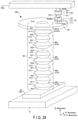
- FIG. 27 , FIG. 28 and FIG. 29 are views illustrating modifications of the magnetic memories of the embodiments.
- a magnetic device in general, includes a magnetic member including a first portion with a first dimension in a first direction, a second portion spaced from with the first portion in a second direction crossing the first direction and having a second dimension in the first direction, a third portion provided between the first portion and the second portion and having a third dimension in the first direction, and a fourth portion provided between the first portion and the third portion and having a fourth dimension in the first direction; and a circuit configured to supply a shift pulse including a first pulse and a second pulse to the magnetic member, and to move a domain wall in the magnetic member in the second direction, wherein the third dimension is less than the first dimension, and the second dimension and the fourth dimension is less than the third dimension, and the first pulse has a first current value, and the second pulse has a second current value which is less than the first current value.
- FIG. 1 to FIG. 19 a magnetic memory of a first embodiment and a control method thereof will be described.
- FIG. 1 to FIG. 4 a configuration example of the magnetic memory of the present embodiment will be described.
- FIG. 1 is a block diagram illustrating a configuration example of the magnetic memory of the present embodiment.
- a magnetic memory 1 of the present embodiment is a domain wall memory.
- the domain wall memory (also referred to as “domain wall shift memory”) 1 of the embodiment includes a memory cell array (also referred to as “memory area”) 100 , a row control circuit 110 , a column control circuit 120 , a write circuit 140 , a read circuit 150 , a shift circuit 160 , an I/O circuit 170 , a voltage generator 180 , and a control circuit 190 .
- the memory cell array 100 includes a plurality of magnetic members 50 and a plurality of interconnects. Each magnetic member 50 is connected to a corresponding one or more interconnects (e.g. a word line and a bit line). Data is stored in a memory cell MC in the magnetic member 50 .
- the row control circuit 110 controls rows of the memory cell array 100 .
- a decoded result (row address) of an address is supplied to the row control circuit 110 .
- the row control circuit 110 sets a row (e.g. a word line), which is based on the decoded result of the address, in a selected state.
- a row e.g. a word line
- the row (or word line) set in the selected state is referred to as “selected row” (or “selected word line”).
- a row other than the selected row is referred to as “non-selected row” (or “non-selected word line”).
- the row control circuit 110 includes a multiplexer (a word line selection circuit) and a word line driver.
- the column control circuit 120 controls columns of the memory cell array 100 .
- a decoded result (column address) of an address from the control circuit 190 is supplied to the column control circuit 120 .
- the column control circuit 120 sets a column (e.g. at least one bit line), which is based on the decoded result of the address, in a selected state.
- the column (or bit line) set in the selected state is referred to as “selected column” (or “selected bit line”).
- a column other than the selected column is referred to as “non-selected column” (or “non-selected bit line”).
- the column control circuit 120 includes a multiplexer (a bit line selection circuit) and a bit line driver.
- the write circuit 140 executes various controls for a write operation (write of data). At a time of a write operation, the write circuit 140 supplies a write pulse, which is formed by current and/or voltage, to the memory cell array 100 . Thereby, data is written in the memory cell array 100 (in memory cells).
- the write circuit 140 is connected to the memory cell array 100 via the row control circuit 110 .
- the write circuit 140 includes a voltage source and/or current source, a pulse generator, a latch circuit, and the like.
- the read circuit 150 executes various controls for a read operation (read of data). At a time of a read operation, the read circuit 150 supplies a read pulse (e.g. read current) to the memory cell array 100 . The read circuit 150 senses a potential or a current value of a bit line BL. Based on the sensed result, data in the magnetic member 50 is read.
- a read pulse e.g. read current
- the read circuit 150 is connected to the memory cell array 100 via the column control circuit 120 .
- the read circuit 150 includes a voltage source and/or current source, a pulse generator, a latch circuit, a sense amplifier circuit, and the like.
- the shift circuit 160 executes various controls for a shift operation (shift of data).
- the shift circuit 160 supplies to the memory cell array 100 a pulse (hereinafter referred to as “shift pulse”) for moving a domain wall (magnetic domain) in the magnetic member 50 .
- the shift circuit 160 is connected to the memory cell array 100 via the row control circuit 110 and the column control circuit 120 .
- the shift circuit 160 includes a voltage source and/or current source, a pulse generator, and the like.
- write circuit 140 read circuit 150 and shift circuit 160 are not limited to mutually independent circuits.
- the write circuit, read circuit and shift circuit may include common structural elements which are mutually usable, and may be disposed in the domain wall memory 1 as a single integral circuit.
- the I/O circuit (input/output circuit) 170 is an interface circuit for transferring various signals.
- the I/O circuit 170 transfers, as write data, data DT from an external device (a controller or a host device) 2 to the write circuit 140 .
- the I/O circuit 170 transfers data, which is output from the memory cell array 100 to the read circuit 150 , to the external device 2 as read data.
- the I/O circuit 170 transfers an address ADR and a command CMD from the external device 2 to the control circuit 190 .
- the I/O circuit 170 transfers various control signals CNT between the control circuit 190 and the external device 2 .
- the voltage generator 180 generates voltages for various operations of the memory cell array 100 , by using a power supply voltage which is provided from the external device 2 (or power supply). For example, at a time of a write operation, the voltage generator 180 outputs various voltages, which are generated for the write operation, to the write circuit 140 . At a time of a read operation, the voltage generator 180 outputs various voltages, which are generated for the read operation, to the read circuit 150 . At a time of a shift operation, the voltage generator 180 outputs various voltages, which are generated for the shift operation, to the shift circuit 160 .
- the control circuit (also referred to as “state machine”, “sequencer” or “internal controller”) 190 controls operations of respective circuits in the memory device 1 , based on the control signal CNT, address ADR and command CMD.
- the control circuit 190 includes, for example, a command decoder, an address decoder, and a latch circuit.
- the command CMD is a signal indicative of an operation which the domain wall memory 1 is to execute.
- the address ADR is a signal indicative of coordinates of at least one memory cell (hereinafter referred to as “selected cell”) which is an operation target in the memory cell array 100 .
- the address ADR includes a row address and a column address of a selected cell.
- the control signal CNT is a signal for controlling an operation timing between the magnetic memory 1 and the external device 2 , and an operation timing in the inside of the magnetic memory 1 .
- FIG. 2 is a schematic view illustrating a configuration example of the memory cell array in the domain wall memory of the present embodiment.
- magnetic members 50 are provided in the memory cell array 100 .
- the magnetic members 50 are arranged two-dimensionally in the memory cell array 100 on a substrate (not shown). Each magnetic member 50 extends in a direction (Z direction) perpendicular to an upper surface (X-Y plane) of the substrate.
- Word lines WL and bit lines BL are provided in the memory cell array 100 .
- the word lines WL are arranged in a Y direction.
- the word lines WL extend in an X direction.
- the bit lines BL are arranged in the X direction.
- the bit lines BL extend in the Y direction.
- the bit lines BL are provided above the word lines WL in the Z direction.
- the magnetic members 50 are provided between the word lines WL and bit lines BL. One end of each magnetic member 50 is connected to the corresponding word line WL. The other end of the magnetic member 50 is connected to the corresponding bit line BL.
- the magnetic members 50 arranged in the X direction are connected to the same word line WL.
- the magnetic members 50 arrange in the Y direction are connected to the same bit line BL.
- a reproducing element 10 and a switching element 20 are connected between the bit line BL and the magnetic member 50 .
- the reproducing element 10 is provided between the magnetic member 50 and the switching element 20 .
- the reproducing element 10 is electrically connected to the magnetic member 50 and the switching element 20 .
- the reproducing element 10 is connected to the magnetic member 50 via a magnetic layer 59 .
- the reproducing element 10 functions as an element (hereinafter, also referred to as “read element”) for reading data in the magnetic member 50 .
- the switching element 20 is provided between the reproducing element 10 and the bit line BL.
- the switching element 20 is electrically connected to the reproducing element 10 and the bit line BL.
- the switching element 20 is used to control a connection between the magnetic member 50 and the bit line BL.
- the switching element 20 is set in the ON state, the magnetic member 50 is electrically connected to the bit line BL.
- the switching element 20 is set in the OFF state, the magnetic member 50 is electrically disconnected from the bit line BL.
- the ON/OFF of the switching element 20 is controlled by the control of a potential difference between the bit line BL and the word line WL.
- one or more magnetic members which are operation targets among the magnetic members 50 of the memory cell array 100 , are selected (activated).
- a conductive layer (interconnect) FL is provided above the magnetic layer 59 in the Z direction.
- the conductive layer FL extends in the X direction, for example, in a region between the bit line BL and the magnetic layer 59 .
- the conductive layer FL extends over a plurality of magnetic layers 59 .
- the conductive layer FL is an interconnect for data write (hereinafter, also referred to as “write line” or “field line”) by a magnetic field write method at a time of a write operation of the domain wall memory 1 .
- a write pulse hereinafter, also referred to as “write current”
- write current By the write current, a magnetic field is generated around the write line FL.
- the generated magnetic field is applied to the magnetic layer 59 .
- the direction of magnetization MM of the magnetic layer 59 and the magnetic member 50 which is connected to the magnetic layer 59 , is set. Thereby, data is written in the magnetic member 50 .
- the direction of the magnetic field changes in accordance with the direction of a write current in the write line FL. Therefore, the direction, in which the write current flows in the write line FL, is set in accordance with the data to be written.
- a plurality of memory cells MC are provided in each magnetic member 50 .
- the memory cells MC are arranged in the Z direction in the magnetic member 50 . Thereby, the memory cells MC are arranged three-dimensionally in the memory cell array 100 .
- Each of the memory cells MC includes a cell region (also referred to as “cell portion” or “data retention portion”) 510 .
- the cell region 510 is a region (portion) provided in the magnetic member 50 in a manner to correspond to the memory cell MC.
- the cell region 510 is a magnetic region (magnetic portion) capable of having magnetization MM.
- the cell region 510 has magnetization MM.
- the data stored in the memory cell MC is associated with the direction of magnetization MM of the cell region 510 .
- the magnetic member 50 has perpendicular magnetic anisotropy or in-plane magnetic anisotropy.
- the magnetization easy axis direction of the cell region 510 corresponds to the magnetic anisotropy of the magnetic member 50 .
- memory cell unit (or “memory cell string”) MU.
- FIG. 3 is a schematic bird's-eye view illustrating a configuration example of the memory cell unit in the domain wall memory of the present embodiment.
- FIG. 4 is a schematic cross-sectional view illustrating a configuration example of the memory cell unit in the domain wall memory of the embodiment.
- the magnetic member 50 is provided above a substrate 9 in the Z direction.
- the magnetic member 50 includes a magnetic layer (hereinafter, also referred to as “domain wall motion layer) 500 .
- the magnetic member 50 extends in the Z direction.
- the magnetic member 50 has a cylindrical structure.
- a center axis of the cylindrical magnetic member 50 extends in the Z direction.
- the center axis of the magnetic member 50 may incline with respect to the Z direction.
- the magnetic member 50 is interposed between two insulators 93 and 95 in a direction parallel to the upper surface of the substrate 9 .
- the insulator 93 may not be provided. In this case, a cavity is provided in the magnetic member 50 .
- the material of the magnetic member 50 is a material including at least one element selected from the group consisting of cobalt (Co), iron (Fe), nickel (Ni), manganese (Mn) and chromium (Cr), and at least one element selected from the group consisting of platinum (Pt), palladium (Pd), iridium (Ir), ruthenium (Ru) and rhodium (Rh).
- a more concrete example of the material of the magnetic member 50 is CoPt, CoCrPt, FePt, CoPd, or FePd. Note that the material of the magnetic member 50 is not limited to the above-described materials, and may be other magnetic materials.
- the magnetic layer constituting the magnetic member 50 may be a stacked film.
- the magnetic member 50 includes a magnetic film and a nonmagnetic film.
- the magnetic film is provided between the nonmagnetic film (e.g. a hafnium oxide film) and the insulator 95 .
- the magnetic film may be provided between the nonmagnetic film and the insulator 93 .
- the magnetic member 50 may be a magnetic film of a single layer.
- the magnetization of the magnetic member 50 is directed in a direction from the center of the magnetic member 50 toward an outer periphery of the magnetic member 50 , or in a direction from the outer periphery of the magnetic member 50 toward the center of the magnetic member 50 .
- the cell region 510 corresponding to each memory cell MC is provided in the magnetic member 50 .
- the magnetic member 50 includes memory cells MC.
- One memory cell MC is provided in one cell region 510 .
- the magnetic layer 59 is provided on the magnetic member 50 in the Z direction.
- the magnetic layer 59 has a circular plan-view shape, as viewed in the Z direction.
- the magnetic layer 59 may have a rectangular plan-view shape.
- a dimension of the magnetic layer 59 in a direction parallel to the surface of the substrate 9 is greater than a dimension D 1 of the magnetic member 50 in the direction parallel to the surface of the substrate 9 .
- the magnetic layer 59 is connected to the magnetic member 50 .
- the magnetic layer 59 is a layer which is continuous with the magnetic member 50 .
- the magnetization of the magnetic layer 59 changes in accordance with the magnetization of the magnetic member 50 .
- the direction of magnetization of the magnetic layer 59 is identical to the direction of magnetization of a cell region 510 A which is directly connected to the magnetic layer 59 .
- the cell region 510 A directly connected to the magnetic layer 59 corresponds to a memory cell MCA which is located closest to the bit line side among the memory cells in the memory cell unit MU.
- the memory cell MCA functions as a read cell at a time of a read operation, and functions as a write cell at a time of a write operation.
- the read cell is a memory cell for temporarily storing data from a memory cell of a read target at a time of a read operation.
- the write cell is a memory cell in which write data is temporarily written at a time of a write operation.
- a stacked body including the reproducing element 10 and switching element 20 is provided on the magnetic layer 59 .
- the reproducing element 10 is a magnetoresistive effect element.
- the magnetoresistive effect element 10 is provided on the magnetic layer 59 in the Z direction.
- the magnetoresistive effect element 10 is disposed in such a position as not to overlap the magnetic member 50 in the Z direction.
- the magnetoresistive effect element 10 may be disposed in such a position as to overlap the magnetic member 50 in the Z direction.
- the magnetoresistive effect element 10 is disposed on one end side in the Y direction of the magnetic layer 59 .
- the magnetoresistive effect element 10 is electrically connected to the magnetic layer 59 .
- the magnetoresistive effect element 10 includes two magnetic layers 11 and 12 and a nonmagnetic layer 13 .
- the nonmagnetic layer 13 is provided between the two magnetic layers 11 and 12 in the Z direction.
- the two magnetic layers 11 and 12 and nonmagnetic layer 13 form a magnetic tunnel junction (MTJ).
- MTJ element the magnetoresistive effect element 10 including the magnetic tunnel junction
- tunnel barrier layer The nonmagnetic layer 13 of the MTJ element 10 is referred to as “tunnel barrier layer”.
- the magnetic layers 11 and 12 are, for example, ferromagnetic layers including cobalt, iron and boron.
- the magnetic layer 11 , 12 may be a single-layer film, or a multilayer film (e.g. artificial lattice film).
- the tunnel barrier layer 13 is, for example, an insulating film including magnesium oxide.
- the tunnel barrier layer 13 may be a single-layer film or a multilayer film.
- Each magnetic layer 11 , 12 has in-plane magnetic anisotropy or perpendicular magnetic anisotropy.
- the magnetization easy axis direction of the magnetic layer 11 , 12 having in-plane magnetic anisotropy is substantially parallel to a layer surface (film surface) of the magnetic layer.
- each magnetic layer 11 , 12 has magnetization which is substantially parallel to the layer surface of the magnetic layer 11 , 12 .
- the direction of magnetization of the magnetic layer 11 , 12 having in-plane magnetic anisotropy is perpendicular to the direction (Z direction) of arrangement of the magnetic layers 11 and 12 .
- the magnetization easy axis direction of the magnetic layer 11 , 12 having perpendicular magnetic anisotropy is substantially perpendicular to the layer surface (film surface) of the magnetic layer.
- each magnetic layer 11 , 12 has magnetization which is substantially perpendicular to the layer surface of the magnetic layer 11 , 12 .
- the direction of magnetization of the magnetic layer 11 , 12 having perpendicular magnetic anisotropy is parallel to the direction (Z direction) of arrangement of the magnetic layers 11 and 12 .
- the direction of magnetization of the magnetic layer 11 is changeable.
- the direction of magnetization of the magnetic layer 12 is unchangeable (in a fixed state).
- the magnetic layer 11 with the changeable magnetization direction is referred to as “storage layer”.
- the magnetic layer 12 with the unchangeable magnetization direction (in the fixed state) is referred to “reference layer”.
- the storage layer 11 is referred to as “free layer”, “magnetization free layer” or “magnetization changeable layer”.
- the reference layer 12 is referred to as “pin layer”, “pinned layer”, “magnetization unchangeable layer” or “magnetization fixed layer”.
- the magnetization direction of the storage layer 11 and the magnetization direction of the magnetic layer 59 change in interlock with each other.
- the magnetization direction of the storage layer 11 is identical to the magnetization direction of the magnetic layer 59 .
- the magnetic layer 59 may be used as a storage layer of the MTJ element 10 .
- the nonmagnetic layer 13 is provided on the magnetic layer 59 such that the nonmagnetic layer 13 is in direct contact with the magnetic layer 59 , without the magnetic layer 11 being disposed.
- the wording “the magnetization direction of the reference layer (magnetic layer) is unchangeable” or “the magnetization direction of the reference layer (magnetic layer) is in the fixed state” means that, when current, voltage or magnetic energy (e.g. magnetic field), with which the magnetization direction of the storage layer changes, is supplied to the magnetoresistive effect element 10 , the magnetization direction of the reference layer does not change before and after the supply of the current, voltage or magnetic energy.
- current, voltage or magnetic energy e.g. magnetic field
- the switching element 20 is provided above the MTJ element 10 in the Z direction.
- the switching element 20 is electrically connected to the MTJ element 10 via, for example, a contact plug CP 1 (or a conductive layer).
- the switching element 20 may be directly connected to the MTJ element 10 , without another member being interposed.
- the switching element 20 includes, for example, two electrodes 21 and 22 and a switching layer 23 .
- the switching layer 23 is provided between the two electrodes 21 and 22 .
- the electrode 21 is provided on the contact plug CP 1 in the Z direction.
- the switching layer 23 is provided on the electrode 21 in the Z direction.
- the electrode 22 is provided on the switching layer 23 in the Z direction.
- the material of the switching layer 23 is, for example, a transition metal oxide, or a chalcogenide compound.
- the switching element 20 switches an electrical connection between the memory cell unit MU and the bit line BL. As a result, activation/deactivation (selection/non-selection) of the memory cell unit MU can be controlled.
- the resistance state of the switching layer 23 changes to a high resistance state or a low resistance state in accordance with a current (or a voltage) supplied to the layer 23 .
- the switching element 20 is set in an ON state (a low resistance state, a conductive state) when a current which is equal to or higher than a threshold current (ON current) of the switching element 20 (or a voltage which is equal to or higher than a threshold voltage) is supplied to the memory cell unit MU.
- the switching element 20 is set in an OFF state (a high resistance state, a non-conductive state) when a current which is lower than the threshold current of the switching element 20 is supplied to the memory cell unit MU.
- the switching element 20 in the OFF state electrically disconnects the memory cell unit MU from the bit line BL.
- the switching element 20 in the ON state can pass current through the memory cell MC.
- the switching element 20 in the ON state supplies the memory cell unit MU with a current flowing from the bit line BL side toward the word line WL side, or a current flowing from the word line WL side toward the bit line BL side, in accordance with a potential difference between the bit line BL and the word line WL.
- the switching element 20 is an element which can pass current through the memory cell unit MU in both directions.
- a conductive layer 70 is provided between the magnetic member 50 and the substrate 9 .
- the conductive layer 70 is provided on an insulating layer 90 which covers the upper surface of the substrate 9 .
- the conductive layer 70 is buried in a trench in the insulating layer 90 .
- the conductive layer 70 extends in the X direction. Note that a magnetic layer or a conductive layer may be provided between the conductive layer 70 and the magnetic member 50 .
- the conductive layer 70 is used as the word line WL.
- the conductive layer 70 functioning as the word line WL is electrically connected to the row control circuit 110 .
- the activation/deactivation (selection/non-selection) of the word line WL is controlled by the row control circuit 110 .
- a conductive layer 71 is provided above the switching element 20 in the Z direction.
- the conductive layer 71 is electrically connected to the switching element 20 via a contact plug CP 2 .
- the conductive layer 71 extends in the Y direction.
- the conductive layer 71 is used as the bit line BL.
- the conductive layer 71 functioning as the bit line BL is electrically connected to the column control circuit 120 .
- the activation/deactivation (selection/non-selection) of the bit line BL is controlled by the column control circuit 120 .
- a conductive layer 75 is provided in an insulating layer 98 between the magnetic layer 59 and the bit line BL.
- the conductive layer 75 neighbors, in the Y direction, the stacked body including the reproducing element 10 and switching element 20 .
- the conductive layer 75 extends in the X direction.
- the conductive layer 75 is used as the write line FL.
- the conductive layer 75 functioning as the write line FL is electrically connected to, for example, the row control circuit 110 and write circuit 140 .
- the activation/deactivation of the write line 75 is controlled by the row control circuit 110 .
- the supply of a write current PWR to the write line FL is controlled by the write circuit 140 .
- the domain wall memory including the memory cell unit illustrated in FIG. 3 and FIG. 4 functions as a domain wall shift memory (e.g. a shift register) of an LIFO (Last-in First-out) method.
- a domain wall shift memory e.g. a shift register
- LIFO Last-in First-out
- the dimension of the magnetic member 50 e.g. the diameter of the cylindrical magnetic layer
- the magnetic member 50 is constricted at predetermined intervals (cycles) in the Z direction.
- Each memory cell MC includes a plurality of projection (convex) portions 511 and 512 and a plurality of concave portions 521 and 522 .
- the projection portions 511 and 512 and concave portions 521 and 522 are one continuous layer in the magnetic member 50 .
- the projection portions 511 and 512 are arranged in the Z direction.
- One memory cell MC includes a first projection portion 511 and a second projection portion 512 .
- the second projection portion 512 is provided on the upper side (on the bit line BL side) of the first projection portion 511 in the Z direction.
- the first projection portion 511 has a first dimension D 1 in the direction parallel to the upper surface of the substrate 9 (e.g. in at least one of the X direction and Y direction).
- the dimension D 1 is a maximum dimension of the projection portion 511 in the X direction (or in the Y direction).
- the dimension D 1 corresponds to the diameter of the magnetic member 50 at a position of the projection portion 511 .
- the projection portion 511 has a dimension L 1 in the Z direction.
- the cross-sectional area of the projection portion 511 is maximum at the position of the dimension D 1 .
- the second projection portion 512 has a second dimension D 2 in the direction parallel to the upper surface of the substrate 9 (e.g. in at least one of the X direction and Y direction).
- the dimension D 2 is a maximum dimension of the projection portion 512 in the X direction (or in the Y direction).
- the dimension D 2 corresponds to the diameter of the magnetic member 50 at a position of the projection portion 512 .
- the dimension D 2 is less than the dimension D 1 .
- the projection portion 512 has a dimension L 2 in the Z direction.
- the dimension L 2 is substantially equal to the dimension L 1 .
- the cross-sectional area of the projection portion 512 is maximum at the position of the dimension D 2 .
- the volume of a magnetic portion (magnetic member), which constitutes the first projection portion 511 , is greater than the volume of a magnetic portion which constitutes the second projection portion 512 .
- each projection portion 511 , 512 has a hexagonal cross-sectional shape as viewed in the X direction (or Y direction).
- the projection portion 511 is also referred as “large projection portion 511 ”, and the projection portion 512 is also referred to as “small projection portion 512 ”.
- the concave portion 521 is provided between the first projection portion (large projection portion) 511 and the second projection portion (small projection portion) 512 .
- the concave portion 521 has a third dimension D 3 in the direction parallel to the upper surface of the substrate 9 .
- the dimension D 3 is less than the dimension D 1 and dimension D 2 .
- the dimension D 3 corresponds to the diameter (e.g. a minimum diameter of the magnetic member) of the magnetic member 50 at a position of the concave portion 521 .
- the concave portion 521 has a dimension L 3 in the Z direction. For example, the dimension L 3 is less than the dimension L 1 and dimension L 2 .
- a dimension (distance) DB between an apex portion of the projection portion 511 and a bottom portion of the concave portion 521 in the X direction (or Y direction) is defined as a depth of a constriction between the projection portion 511 and the concave portion 521 .
- the apex portion of the projection portion 511 is a portion of the projection portion 511 , which has the maximum dimension D 1 .
- the bottom portion of the concave portion 521 is a portion having the dimension D 3 of the concave portion 521 .
- a dimension (distance) DA between the projection portion 512 and the concave portion 521 in the X direction (or Y direction) is defined as a depth of a constriction between an apex portion of the projection portion 512 and a bottom portion of the concave portion 521 .
- the apex portion of the projection portion 512 is a portion of the projection portion 512 , which has the maximum dimension D 2 .
- the projection portions 511 and 512 and the concave portion 521 are provided between two concaves portions 522 ( 522 a , 522 b ) in the Z direction.
- One concave portion 522 a is provided on one end side in the Z direction of the cell region 510 .
- the other concave portion 522 b is provided on the other end side in the Z direction of the cell region 510 .
- Each concave portion 522 is provided between two mutually neighboring memory cells MC in the Z direction.
- the concave portion 522 has a dimension D 4 in the direction (e.g. at least one of the X direction and Y direction) parallel to the upper surface of the substrate 9 .
- the dimension D 4 corresponds to the diameter (e.g. minimum diameter) of the magnetic member 50 at a position of the concave portion 522 .
- the dimension D 4 is less than the dimension D 1 and dimension D 2 .
- the dimension D 4 is substantially equal to the dimension D 3 .
- the concave portion 521 has a dimension L 4 in the Z direction.
- the dimension L 4 is substantially equal to the dimension L 3 .
- a domain wall is retained in the concave portion 522 in accordance with the state of magnetization (magnetic domain) of mutually neighboring memory cells MC (projection portions 511 and 512 ).
- the concave portion 522 is also referred to as “domain wall retention portion 522 ” (or “domain wall existence region 522 ”).
- the concave portion 522 between one memory cell MC and the other memory cell MC functions as a domain wall retention portion of the one memory cell MC.
- One end of the other memory cell MC functions as a domain wall retention portion of the one memory cell MC, and the other end of the other memory cell MC functions as a domain wall retention portion of the other memory cell MC.
- each concave portion 522 is shared by two memory cells MC which neighbor in the Z direction.
- Each concave portion 522 is used as the domain wall retention portion of one of the two memory cells MC which share the concave portion 522 .
- the concave portion 522 is disposed at a boundary of the mutually neighboring memory cells MC.
- One projection portion 511 , one projection portion 512 and one concave portion 521 are, at least, provided in one cell region 510 .
- a structure including at least the projection portions 511 and 512 and concave portion 521 forms a region of one cycle in the magnetic member 50 having a cyclic constriction structure.
- the structure of one cycle is used as one memory cell MC.
- each of the projection portions 511 and 512 includes a portion having a certain dimension in the magnetic member 50 , and a region of a certain size centering on the portion having this dimension.
- each of the concave portions (hereinafter, also referred to as “constriction portions” or “constriction regions”) 521 and 522 includes a portion having a certain dimension in the magnetic member 50 , and a region of a certain size centering on the portion having this dimension.
- the dimensions of the respective portions in the cylindrical magnetic member 50 are set with reference to a plane on the outer peripheral side (outer wall side) of the magnetic member 50 .
- the dimensions of the respective portions may be defined with reference to a plane on the inner peripheral side (inner wall side) of the magnetic member 50 .
- the magnetic member 50 may include a portion of a fixed dimension (a region with an invariable dimension) in a direction crossing the direction of motion of the domain wall in the projection portion 511 , 512 and the concave portion 521 , 522 .
- the shift of data in the memory cell unit MU is executed by a shift operation on the domain wall in the magnetic member 50 .
- a domain wall retained in a certain memory cell MC is moved (shifted) to another memory cell MC by a shift pulse (e.g. a current pulse) supplied to the magnetic member 50 .
- a shift pulse e.g. a current pulse
- the domain wall is shifted by one cycle (one memory cell) by one-time supply of a shift pulse.
- magnetic domains in the memory cells MC move.
- the concave portion (constriction portion) 521 is provided in each memory cell MC.
- the large projection portion 511 and small projection portion 512 are arranged in the extending direction of the magnetic member 50 , with the concave portion 521 being interposed.
- the dimension D 1 of the large projection portion 511 in the parallel direction to the upper surface of the substrate 9 is greater than the dimension D 2 of the small projection portion 512 in the parallel direction to the upper surface of the substrate 9 .
- the large projection portion 511 is located on the source-of-motion side of the domain wall
- the small projection portion 512 is located on the destination-of-motion side of the domain wall.
- a domain wall exists in a concave portion 522 a on one side of a certain cell region 510 (a domain wall retention portion 522 a of a certain memory cell).
- this domain wall is shifted into a concave portion 522 b on the other side of the cell region 510 (a domain wall retention portion 522 b of the neighboring cell) via the concave portion 521 (and projection portions 511 and 512 ), by using a shift pulse which includes two pulses.
- the volume of the first projection portion (large projection portion) 511 having the first dimension D 1 is greater than the volume of the second projection portion (small projection portion) 512 having the second dimension D 2 .
- the energy for the domain wall to move in the first projection portion 511 is greater than the energy for the domain wall to move in the second projection portion 512 .
- the first projection portion 511 functions as a stopper (barrier) of motion of the domain wall, with respect to the shift current of a certain current value at the time of the shift operation.
- the domain wall memory of the present embodiment can suppress excessive motion of the domain wall between the memory cells. Therefore, the domain wall memory of the present embodiment can decrease an error of the position of the domain wall which is moved by the shift operation to a target position.
- the domain wall memory of the present embodiment can suppress a shift error of the domain wall.
- each of the projection portion 511 and projection portion 512 in the magnetic member 50 has a substantially symmetric shape with respect to the direction of motion of the domain wall (here, in the Z direction), with the position having the maximum dimension of each portion 511 , 512 being set as the center.
- the projection portions 511 and projection portions 512 are alternately arranged in the magnetic member 50 in the direction of motion of the domain wall.
- the domain wall memory of the present embodiment when the domain wall is shifted from one end side (e.g. word line side) of the magnetic member 50 to the other end side (e.g. bit line side) of the magnetic member 50 , or when the domain wall is shifted from the other end side of the magnetic member 50 to the one end side of the magnetic member 50 , in response to a predetermined shift pulse which is supplied, it is possible to suppress a variance in shift amount (motion distance) of the domain wall due to asymmetry in shape of each projection portion.
- one end side e.g. word line side
- the other end side e.g. bit line side
- the pulse shape of the shift pulse in the case where the domain wall is moved from the one end side of the magnetic member 50 to the other end side (e.g. bit line side) of the magnetic member 50 can be made substantially identical to the pulse shape of the shift pulse in the case where the domain wall is moved from the other end side of the magnetic member 50 to the one end side of the magnetic member 50 .
- FIG. 5 to FIG. 9 are cross-sectional process views illustrating fabrication steps of the manufacturing method of the magnetic memory (e.g. domain wall memory) of the present embodiment.
- the magnetic memory e.g. domain wall memory
- a plurality of layers 911 , 912 , 913 and 915 are formed on the upper surface of the substrate 9 at predetermined cycles (arrangement).
- interconnects (not shown) having a predetermined pattern are formed in an insulating layer (not shown) on the substrate 9 or on an insulating layer on the substrate 9 .
- a hafnium oxide layer (also referred to as “hafnia layer”) (HfO 2 layer) 911 is formed on the substrate 9 .
- a silicon oxide layer (SiO 2 layer) 912 is formed above the HfO 2 layer 911 in the Z direction.
- a hafnium oxide layer 911 is formed above silicon oxide layer 912 .
- a hafnium silicon oxide layer (also referred to as “hafnium silicate layer”) (HfSiO 4 layer) 913 is formed above the hafnium oxide layer 911 in the Z direction.
- a HfO 2 layer 911 is formed on the HfSiO 4 layer 913 .
- a SiO 2 layer 912 is formed above the HfSiO 4 layer 913 via the HfO 2 layer 911 . In this manner, the SiO 2 layer 912 and the HfSiO 4 layer 913 are alternately formed in the Z direction, with the HfO 2 layer 911 being interposed.
- the layers 911 , 912 and 913 are formed such that the concentrations of constituent elements in the layers 911 , 912 and 913 vary in the Z direction.
- intermediate layers (hereinafter, also referred to as “concentration modulation layers”) 915 are provided between the layers 911 , 912 and 913 .
- the intermediate layer 915 is a region where the concentrations of constituent elements in layers gradually vary from a central portion of one layer toward a central portion of the other layer. Between two layers, the concentration of a certain constituent element of one layer has a maximum value at a central portion of the one layer, and gradually decreases in the intermediate layer 915 toward a central portion of the other layer.
- FIG. 6 is a schematic view for explaining variations of the concentrations of constituent elements in a stacked body.
- FIG. 6 illustrates a variation (line CON-Hf) of the concentration of Hf and a variation (line CON-Si) of the concentration of Si in a stacked body 900 .
- the concentration of Hf is highest in a central portion of the HfO 2 layer 911 and gradually lowers toward the SiO 2 layer 912 .
- the concentration of Si is highest in a central portion of the SiO 2 layer 912 and gradually lowers toward the HfO 2 layer 911 .
- the Hf element is replaced with the Si element.
- the Si element is replaced with the Hf element.
- the region 915 between the central portion of the HfO 2 layer 911 and the central portion of the SiO 2 layer 912 becomes an oxide region including Hf and Si.
- the intermediate layer 915 is formed between the HfO 2 layer 911 and the SiO 2 layer 912 .
- the intermediate layer 915 is a (HfO 2 ) x (SiO 2 ) 1-x layer (0 ⁇ x ⁇ 1).
- the Hf concentration in the intermediate layer 915 is lower than the Hf concentration in the central portion of the HfO 2 layer 911 , and is higher than the Hf concentration in the central portion of the SiO 2 layer 912 .
- the Si concentration in the intermediate layer 915 is lower than the Si concentration in the central portion of the SiO 2 layer 912 , and is higher than the Si concentration in the HfO 2 layer 911 .
- the properties of the layers 911 , 912 and 915 vary in the Z direction.
- the Hf element is replaced with the Si element from the HfO 2 layer 911 toward the intermediate layer 915 .
- the Si element is replaced with the Hf element from the HfSiO 4 layer 913 toward the intermediate layer 915 .
- the Hf concentration of the intermediate layer 915 is lower than the Hf concentration in the central portion of the HfO 2 layer 911 and is higher than the concentration in the central portion of the HfSiO 4 layer 913 .
- the Si concentration of the intermediate layer 915 is lower than the concentration in the central portion of the HfSiO 4 layer 913 .
- the properties of the layers 911 , 913 and 915 vary in the Z direction.
- the HfO 2 layers (HfO 2 regions) 911 , SiO 2 layers (SiO 2 regions) 912 , HfSiO 4 layers (HfSiO 4 regions) 913 and intermediate layers ((HfO 2 ) x (SiO 2 ) 1-x regions) 915 are formed in the stacked body 900 such that the concentration distribution of Hf and the concentration distribution of Si in the stacked body 900 vary with gradients in the Z direction.
- the example is illustrated in which the stacked body 900 is formed by using the layers including Hf and the layers including Si.
- materials of the layers that form the stacked body 900 use may be made of other insulators, for example, oxynitrides, silicates and aluminates, such as a nitride of silicon (also referred to as “silicon nitride” (SiN), silicon oxynitride (SiON), zirconium-silicon oxide (zirconium silicate) (ZrSiO), hafnium-aluminum oxide (hafnium aluminate) (HfAlO), and hafnium-silicon oxynitride (HfSiON).
- SiN silicon nitride
- SiON silicon oxynitride
- zirconium-silicon oxide zirconium silicate
- hafnium-aluminum oxide hafnium aluminate
- HfAlO hafnium
- a hole 990 is formed in the stacked body 900 by lithography and anisotropic etching (e.g. reactive etching).
- the hole 990 extends in the Z direction in the stacked body 900 .
- a bottom portion of the hole 990 reaches the upper surface of the substrate 9 .
- each layer has a substantially uniform thickness in the layer, and layer surface of each layer is parallel to the upper surface of the substrate.
- the plan-view shape of the hole 990 as viewed in the Z direction is circular (or elliptic).
- the hole 990 has a cylindrical structure.
- the plan-view shape of the hole 990 as viewed in the Z direction may be rectangular.
- isotropic etching e.g. wet etching
- the side surfaces of the layers 911 , 912 , 913 and 915 in the hole 990 retreat in a parallel direction to the upper surface of the substrate 9 by the isotropic etching.
- the condition for the isotropic etching is set such that a large etching selectivity can be secured between the layer 911 including hafnium and the layer 912 including silicon.
- wet etching is performed by using hydrofluoric acid as an etching solution.
- the etching amount (etching rate) of each layer 911 , 912 , 913 and 915 varies depending on the Si concentration in the layer.
- the etching amount of the SiO 2 layer 912 is greater than the etching amount of the HfO 2 layer 911 .
- the etching amount of each of the HfSiO 4 layer 913 and the intermediate layer 915 is less than the etching amount of the SiO 2 layer and is greater than the etching amount of the HfO 2 layer.
- the side surface of the SiO 2 layer 912 , the side surface of the HfSiO 4 layer 913 and the side surface of the intermediate layer 915 retreat in the parallel direction to the upper surface of the substrate 9 , compared to the side surface of the HfO 2 layer 911 .
- a recess 941 is formed at the position of the SiO 2 layer 912 (and intermediate layer 915 ), and a recess 942 is formed at the position of the HfSiO 4 layer 913 (and intermediate layer 915 ).
- a depth G 1 of the recess 941 in the parallel direction to the upper surfaced of the substrate 9 is greater than a depth G 2 of the recess 942 in the parallel direction to the upper surface of the substrate 9 .
- the recesses 941 and 942 with different depths are formed in the stacked body 900 .
- a hole having a cyclically constricted structure in the Z direction (a hole having an opening dimension varying in the Z direction) is formed in the stacked body 900 .
- the cross-sectional shape of the recess 941 , 942 becomes triangular.
- a magnetic layer 500 is formed on a side surface of the stacked body 900 .
- the magnetic layer 500 covers the side surfaces of the layers 911 , 912 , 913 and 915 of the stacked body 900 in the hole 990 , along the shapes of the recesses 941 and 942 .
- the magnetic member 50 extending in the Z direction is formed in the stacked body 900 .
- the magnetic member 50 includes the projection portions 511 and 512 and the concave portions 521 and 522 .
- the magnetic member 50 has a cylindrical shape.
- the projection portion 511 of the magnetic member 50 is formed in the recess 941 .
- the projection portion 512 is formed in the recess 942 .
- the concave portion 521 , 522 is formed in a region between the recess 941 and recess 942 in the Z direction.
- the magnetic member 50 is constricted in accordance with the shapes of the recesses 941 and 942 .
- the dimension in the Y direction of the magnetic member 50 at the position of the recess 941 is greater than the dimension in the Y direction of the magnetic member 50 at the position of the recess 942 .
- the magnetic member 50 having the constriction structure is formed above the substrate 9 .
- the reproducing element, switching element and various interconnects are formed above the magnetic member 50 .
- the memory cell unit in the domain wall memory of the present embodiment is formed.
- the domain wall memory of the present embodiment is formed.
- the hole with the constriction structure, which forms the magnetic member 50 may be formed by using anodic oxidation of a metal (e.g. aluminum).
- a metal e.g. aluminum
- FIG. 10 is a schematic diagram for explaining a shift operation of the domain wall memory of the present embodiment.
- the memory cells MC (MC ⁇ 1> to MC ⁇ 5>) have magnetizations (magnetic domains) MM 1 , MM 2 , MM 3 , MM 4 and MM 5 corresponding to stored data.
- the magnetic member 50 has perpendicular magnetic anisotropy.
- a magnetization which is directed to the outside (outer peripheral side) of the cylindrical magnetic member 50 , is associated with first data (one of “0” data and “1” data)
- a magnetization which is directed to the inside (center axis side) of the cylindrical magnetic member 50 , is associated with second data (the other of “0” data and “1” data).
- a domain wall DW is disposed in the concave portion 522 between the mutually neighboring memory cells.
- the cell regions (magnetic portions) 510 corresponding to two mutually neighboring memory cells MC with different magnetization directions have magnetic domains MD (MD 1 , MD 2 , MD 3 , and MD 4 ) separated by the domain wall DW.
- the mutually neighboring cell regions 510 with the identical magnetization direction have one magnetic domain MD which is continuous between the two cell regions 510 .
- one magnetic domain MD is formed to include three or more consecutive cell regions 510 , depending on the arrangement of “1” and “0” of data stored in the memory cell unit.
- one magnetic domain MD 2 is formed to include two consecutive cell regions 510 in which the memory cells MC ⁇ 2> and MC ⁇ 3> are provided.
- domain walls DW are formed between the cell region 510 , in which the memory cell MC ⁇ 4> is provided, and the cell region 510 , in which the memory cell MC ⁇ 3> is provided, and between the cell region 510 , in which the memory cell MC ⁇ 4> is provided, and the cell region 510 , in which the memory cell MC ⁇ 5> is provided.
- magnetic domains MD 2 , MD 3 and MD 4 which are separated by the domain walls DW, are formed in the cell region 510 of the memory cell MC ⁇ 3>, the cell region 510 of the memory cell MC ⁇ 4> and the cell region 510 of the memory cell MC ⁇ 5>, respectively.
- the magnetic domain MD 1 of the memory cell MC ⁇ 1> is separated by the domain wall DW from the magnetic domain MD 2 in the cell regions 510 of the memory cells MC ⁇ 2> and MC ⁇ 3>.
- a shift pulse SP is supplied to the magnetic member 50 .
- the direction of motion of electrons (e ⁇ ) is opposite to the direction of motion of the shift pulse SP that is an electric current.
- the shift pulse SP flows in the magnetic member 50 .
- electrons (e ⁇ ) move in a direction from the memory cell MC ⁇ 1> toward the memory cell MC ⁇ 5>.
- the motion of the domain wall DW in the shift operation is due to STT (Spin transfer torque) and/or SOT (Spin orbit torque) occurring in the magnetic member.
- the magnetization (magnetic domain) MD in the cell region 510 moves.
- the magnetic domain MD 1 of the cell region 510 in the memory cell MC ⁇ 1> prior to the shift operation moves to the cell region 510 in the memory cell MC ⁇ 2> by the shift operation.
- a magnetic domain MD 0 (magnetization MM 0 ) of a neighboring memory cell moves to the cell region 510 in the memory cell MC ⁇ 1>.
- the magnetic domain MD is shifted by one memory cell (by one bit) by the motion of the domain wall DW.
- the shift operation motion of the domain wall/magnetic domain
- a pulse e.g. a current pulse
- the domain wall DW moves in two steps to the concave portion 522 via the concave portion 521 .
- the domain wall DW can exist more stably in the magnetic region with a small volume (e.g. the concave portion in this embodiment), than in the magnetic region with a large volume (e.g. the projection portion in this embodiment).
- the domain wall DW which is moved by the shift operation, is located in the concave portion 521 , 522 (and in a region near the concave portion 521 , 522 ), compared to the projection portion 511 , 512 .
- the shift pulse SP includes a plurality of pulses.
- the domain wall DW is moved in the memory cell unit MU such that the domain wall DW is located in the concave portion (domain wall retention portion) 522 of the memory cell MC via the concave portion 521 .
- the direction of motion of the domain wall at the time of the pulse operation can be controlled by the material of the magnetic member, the material of a conductive member stacked on the magnetic member, the position of the conductive member relative to the magnetic member, and manufacturing conditions.
- a conductive member is stacked on the magnetic member, for example, platinum (Pt), tungsten (W), tantalum (Ta), etc. can be used as the material of the conductive member.
- the materials of the conductive member are not limited to these.
- the magnetic member 50 may have in-plane magnetic anisotropy.
- the magnetization easy axis direction of the magnetic member 50 is parallel to the Z direction.
- magnetic layers with in-plane magnetic anisotropy may be used for the magnetic layers 11 and 12 of the MTJ element 10 .
- FIG. 11 is a waveform diagram illustrating a shift pulse used in the shift operation of the domain wall memory of the present embodiment.
- the abscissa axis of FIG. 11 corresponds to time, and the ordinate axis of FIG. 11 corresponds to an absolute value of a current value.
- the shift pulse SP is supplied during a period (hereinafter referred to as “shift operation period”) TS of the shift operation.
- shift pulse SP is, for example, a current pulse.
- the shift current SP includes a first pulse P 1 and a second pulse P 2 .
- the pulses P 1 and P 2 which are supplied, the energy for moving the domain wall is applied to the domain wall in the magnetic member.
- the first pulse P 1 has a current value ia.
- the first pulse P 1 has a pulse width t p1 .
- the second pulse P 2 has a current value ib.
- the second pulse P 2 has a pulse width t p2 .
- the current value ia is equal to or greater than a current value iax.
- the current value iax is a current value of a critical current for moving the domain wall DW from the concave portion 522 to the concave portion 521 via the projection portion 511 .
- the current value ib is equal to or greater than a current value ibx.
- the current value ibx is a current value of a critical current for moving the domain wall DW from the concave portion 521 to the concave portion 522 via the projection portion 512 .
- the current values iax and ibx are higher than a threshold (hereinafter, also referred to as “domain wall shift threshold”) ith of motion (shift) of the domain wall in the magnetic member 50 of the constriction structure.
- domain wall shift threshold a threshold ith of motion (shift) of the domain wall in the magnetic member 50 of the constriction structure.
- the domain wall shift threshold in the magnetic member 50 of the constriction structure is indicative of a current value at which the domain wall begins to move (shift) by the function of energy due to SOT and/or STT by current (electrons).
- the domain wall shift threshold ith in the magnetic member 50 of the constriction structure can be calculated by a product of a minimum value of a cross-sectional area (e.g. a cross-sectional area of the concave portion 522 as viewed in the Z direction) of the cell region 510 in the Z direction and a critical current density for the shift of the domain wall.
- the critical current density for the shift of the domain wall in the magnetic member varies depending on the material of the magnetic member and the structure of the magnetic member.
- the cross-sectional area at the position of the concave portion 522 (or concave portion 521 ) in the magnetic member 50 is a minimum value of the cross-sectional area of the cell region 510 (magnetic member 50 ).
- the domain wall in the concave portion 522 shifts toward the projection portion 511 (or projection portion 512 ).
- the domain wall cannot move beyond the apex portion of the projection portion 511 even if the domain wall shifts to a region between the apex portion of the projection portion 511 (a portion with a maximum cross-sectional area of the projection portion 511 ) and the concave portion 522 . Therefore, before and after the supply of the current of the current value ith to the magnetic member, the position of the domain wall DW in the concave portion 522 does not substantially change.
- the magnitude of the pulse width t p2 is substantially equal to the magnitude of the pulse width t p1 .
- the magnitude of the pulse width t p2 may be different from the magnitude of the pulse width t p1 .
- each pulse width (t p1 and t p2 ) is a value based on a full width at half maximum of each pulse (P 1 and P 2 ).
- the pulse width t p1 and t p2 may be defined based on a standard other than the full width at half maximum.
- the pulse width t p1 of the pulse P 1 has a magnitude based on a period during which the domain wall in the domain wall retention portion 522 of a certain memory cell moves into the projection portion 512 (or concave portion 521 , 522 ) of a memory cell MC neighboring by one cycle, when the shift current of a certain current value ia is supplied.
- the pulse width t p2 of the pulse P 2 has a value based on a period during which the domain wall in the domain wall retention portion 521 moves to the concave portion (domain wall retention portion) 522 of the memory cell MC (or a region between the apex portion of the projection portion 512 of a certain memory cell MC ⁇ k> and the apex portion of the projection portion 511 of another memory cell MC ⁇ k+1>).
- the apex portion of the projection portion 511 corresponds to a portion with the maximum dimension D 1 in the projection portion 511 .
- the apex portion of the projection portion 512 corresponds to a portion with the maximum dimension D 2 in the projection portion 512 .
- the pulse width (the time of motion of the domain wall DW) t p1 of the pulse P 1 is set in accordance with a time for the motion over a dimension which is equal to or greater than the dimension L 1 in the Z direction from the concave portion (the domain wall retention portion of the memory cell MC) 522 to the concave portion 521 in the direction of motion of the domain wall (the dimension of the projection portion 511 in the direction of motion of the domain wall DW), and which is less than a dimension “L 1 +L 2 ” from the concave portion 522 to the concave portion 522 in the direction of motion of the domain wall, when the shift current of a certain current value is ia supplied.
- the dimension L 3 (L 4 ) in the Z direction of the concave portion 521 ( 522 ) is set to be sufficiently smaller than the dimension L 1 (L 2 ).
- the dimensions L 3 and L 4 are approximated to zero.
- the distance of motion of the domain wall at a time when the pulse P 1 of the pulse width t p1 is supplied is a value approximated to a distance to a substantially middle position between two projection portions 511 which neighbor in the direction of motion of the domain wall.
- the distance of motion of the domain wall at the time of supply of the pulse P 1 is approximated to a distance “L 1 +L 2 /2” [to a middle position between the position of L 1 /2 of the projection portion 511 and the position (L 1 /2+L 1 +L 2 ) of a projection portion 511 which neighbors in the direction of motion of the domain wall, with the projection portion 512 being interposed].
- the velocity of motion of the domain wall DW between the concave portions 522 and 521 can be calculated by using the time of motion of the domain wall DW (the pulse width of the pulse) and the distance L 1 between the two concave portions 522 and 521 .
- the actual length of the magnetic portion which functions as the projection portion 511 (or projection portion 512 ) is approximated to the dimension L 1 in the Z direction of the projection portion 511 (or the dimension L 2 in the Z direction of the projection portion 512 ).
- the current values ia and ib have a relationship of a mathematical expression (eq1) below.
- the maximum value of the cross-sectional area of the projection portion (large projection portion) 511 is indicated by “A L ”
- the maximum value of the cross-sectional area of the projection portion (small projection portion) 512 is indicated by “A S ”.
- the critical current density for moving the domain wall is indicated by “Jc”.
- a motion velocity v DW of the domain wall can be expressed by the following equation (eq2).
- v DW C ⁇ (( J/Jc ) 2 ⁇ 1) 1/2 (eq2)
- C is a proportionality factor
- J is a current density of current used in the shift.
- the current density in the pulse P 1 of the current value ia is indicated by “Ja”.
- the current density in the pulse P 2 of the current value ib is indicated by “Jb”.
- A(z) is indicative of a cross-sectional area at a position (z) in the Z direction in the magnetic member 50 .
- the current value of the pulse current Iz is constant without depending on the position in the magnetic member 50 .
- the motion distance L of the domain wall is controlled in accordance with the current value of the pulses P 1 and P 2 , which serves as the current Iz, and the pulse width tp of the pulses P 1 and P 2 .
- the magnitude of the current ib (and the magnitude of the pulse width t p2 ) is set such that the domain wall DW in the concave portion 521 , 522 of a certain memory cell MC ⁇ k> does not shift into a neighboring memory cell MC ⁇ k+1>.
- the two pulses P 1 and P 2 of the shift current SP have mutually different current values ia and ib.
- a period (hereinafter, also referred to as “relaxation period”) t rx1 is provided between the first pulse P 1 and the second pulse P 2 .
- the relaxation period t rx1 corresponds to a time until magnetization enters an equilibrium state.
- the magnetic state of the shifted domain wall DW stabilizes.
- a certain period (relaxation period) t rx2 is provided from the stop of the supply of the second pulse P 2 to the terminal end of the shift operation (the start of the next supply of the shift current SP).
- the relaxation period t rx2 after the supply of the second pulse P 2 the magnetic state of the domain wall moved by the pulse P 2 is stabilized.
- FIG. 12 is a waveform diagram illustrating a modification of the shift current of the domain wall memory of the present embodiment.
- the current value of the shift current SP may have a value ic which is greater than 0, in the period (relaxation period) between the two pulses P 1 and P 2 .
- the current value ic is greater than 0 and less than the domain wall shift threshold ith.
- the two pulses P 1 and P 2 of the shift current have a continuous pulse shape with a current value of 0 or more.
- the domain wall memory of the present embodiment can shift the domain wall, in two motion steps, to a predetermined position (target position) in the magnetic member 50 having the constriction structure, by the shift current SP including the two pulses P 1 and P 2 with different current values, as illustrated in FIG. 11 and FIG. 12 .
- FIG. 13 to FIG. 17 are schematic views illustrating states of motion of the domain wall at the time of the shift operation in the domain wall memory of the present embodiment.
- FIG. 13 to FIG. 17 illustrate distributions of existence probability of the domain wall (DW) in the magnetic member.
- FIG. 13 also illustrates, for the purpose of clearer description, the transition of the variation of the cross-sectional area of the magnetic member in relation to the position in the magnetic member of the constriction structure.
- the cross-sectional area at a certain position in the magnetic member has a correlation with the volume of the domain wall at that position in the magnetic member. Therefore, based on the width of the domain wall and the cross-sectional area of the magnetic member in relation to the position in the magnetic member, the magnitude of the volume of the magnetic member in relation to the position in the magnetic member can equivalently be calculated.
- the domain wall DW prior to the supply of the shift current, the domain wall DW is retained in a memory cell MC ⁇ k ⁇ 1>.
- the domain wall DW is disposed in a concave portion 522 ⁇ k ⁇ 1> of the memory cell MC ⁇ k ⁇ 1> or a region near the concave portion 522 ⁇ k ⁇ 1> with a certain existence probability Q 0 .
- the shift current SP including two pulses P 1 and P 2 is supplied to the magnetic member 50 .
- the first pulse P 1 having a current value ia (ia>iax) is supplied to the magnetic member 50 .
- the pulse P 1 has a pulse width t p1 .
- a current corresponding to the current value ia flows in the magnetic member 50 during a period corresponding to the pulse width t p1 .
- the domain wall DW in the concave portion 522 moves from the memory cell MC ⁇ k ⁇ 1> into the neighboring memory cell MC ⁇ k>.
- the domain wall DW moves along the direction of motion of electrons.
- the domain wall DW moves into a projection portion 512 ⁇ k> via a projection portion 511 ⁇ k> by the pulse P 1 .
- the current value ia and pulse width t p1 of the pulse P 1 are set such that the domain wall DW moves to an intermediate position (e.g. a position C 1 ) between the projection portion 511 ⁇ k> and a projection portion 511 ⁇ k+1>.
- a distribution Q 1 of the existence probability of the domain wall DW in the region from the projection portion 511 ⁇ k> to the projection portion 511 ⁇ k+1> is wider than a distribution Q 0 .
- a standard deviation ⁇ of the existence probability distribution of the domain wall and a motion distance L of the domain wall vary while keeping the relation of ⁇ 2 /L substantially constant, when a motion velocity v of the domain wall is assumed to be constant.
- the shift operation After the supply of the pulse P 1 , the shift operation temporarily enters a standby state during a period (relaxation period) t rx1 from the stop of supply of the pulse P 1 to the start of supply of the pulse P 2 .
- the magnetic state of the projection portion 511 , 512 and concave portion 521 , 522 transitions into a relaxation state (equilibrium state) by the stop of supply of the pulse P 1 .
- the moved domain wall moves to a portion with a smaller volume (a portion with a smaller dimension) in the magnetic member 50 from the portion where the domain wall currently exists, such that the domain wall enters a stabler energy state.
- domain walls DWa and DWb in the memory cell MC ⁇ k> shift from the projection portion 512 ⁇ k> to concave portion 521 ⁇ k> or from the projection portion 512 ⁇ k> to concave portion 522 ⁇ k>.
- the existence probability (distributions Q 2 a and Q 2 b ) of the domain walls DWa and DWb in the memory cell MC ⁇ k> increases in a region near the boundary between the projection portion 512 ⁇ k> and concave portion 521 ⁇ k> or in a region near the boundary between the projection portion 512 ⁇ k> and concave portion 522 ⁇ k>.
- the pulse P 2 having a current value ib (iax>ib>ibx) is supplied to the magnetic member 50 .
- the current value ib of the pulse P 2 is set to a current value which is equal to or greater than such a current value that the domain wall DWa can move beyond a portion (a position with the dimension D 2 ) having a maximum value VL 2 of the volume (a maximum cross-section AL 2 ) in the projection portion 512 .
- the pulse P 2 has a pulse width t p2 . Thereby, a current corresponding to the current value ib flows in the magnetic member 50 during a period corresponding to the pulse width t p2 .
- the domain wall DW exists in the region near the concave portion 521 ⁇ k> or the region near the concave portion 522 ⁇ k>.
- the domain wall DWa in the concave portion 521 ⁇ k> moves beyond the projection portion 512 ⁇ k> into the concave portion 522 ⁇ k> by the energy due to the pulse P 2 with the current value ib.
- the current value ib of the pulse P 2 is set to such a current value (e.g. a value less than the current value ia) that the domain wall DWb does not move beyond a portion (a position with the dimension D 1 ) having a maximum value VL 1 of the volume (a maximum cross-section AL 1 ) in the projection portion 511 .
- the energy (e.g. spin torque), which the domain wall in the concave portion 521 ⁇ k> receives from the pulse P 2 is the energy by which the domain wall DWb can move into the projection portion 512 ⁇ k>, but is less than the energy by which the domain wall DWb can move into the concave portion 521 ⁇ k+1> via the projection portion 511 ⁇ k+1>.
- the domain wall DWb can move beyond the projection portion 512 ⁇ k> but cannot move beyond the projection portion 511 ⁇ k+1>.
- the domain wall DWb in the concave portion 522 ⁇ k> receives the pulse P 2 of the current value ib.
- the current value ib of the pulse P 2 is set to such a current value (e.g. a value less than the current value ia) that the domain wall DWb does not move beyond a portion (a position with the dimension D 1 ) C 3 having the maximum value VL 1 of the volume in the projection portion 511 .
- the energy e.g.
- the domain wall DWb does not move beyond the projection portion 511 ⁇ k+1>.
- a domain wall DWz at the time when the pulse P 2 is supplied is located in the region between the position (the portion with the dimension D 2 ) C 2 having the maximum value of the volume (the maximum cross-section) of the projection portion 512 ⁇ k> and the position (the portion with the dimension D 1 ) C 3 having the maximum value of the volume (the maximum cross-section) of the projection portion 511 ⁇ k+1>.
- the domain wall DW moves, for example, by an internal magnetic field occurring in the magnetic member of the constriction structure, to a portion (a portion with a smaller dimension) having a smaller volume than the volume of the portion where the domain wall is currently disposed in the magnetic member 50 , in such a manner that the domain wall DW enters a stabler energy state.
- the domain wall which may exist between the concave portion 522 ⁇ k> and the projection portion 512 ⁇ k>, stabilizes in the concave portion 522 ⁇ k>.
- the domain wall which may exist between the concave portion 522 ⁇ k> and the projection portion 511 ⁇ k+1>, moves to the concave portion 522 ⁇ k>.
- the domain wall which may exist between the concave portion 522 ⁇ k> and the projection portion 511 ⁇ k+1>, shifts to the concave portion 522 ⁇ k> side.
- the domain wall which is shifted by the shift current SP (pulse P 2 ) from the concave portion 522 ⁇ k> of a certain memory cell MC ⁇ k> to the projection portion 511 ⁇ k+1> side of a neighboring memory cell MC ⁇ k+1>, moves back into the concave portion 522 ⁇ k>.
- the domain wall in the projection portion 512 ⁇ k> shifts to the concave portion 522 ⁇ k> side having a smaller volume (a smaller cross-section area).
- an existence probability distribution Q 4 of the domain wall DW exhibits a high existence probability in the concave portion (the domain wall retention portion) 522 ⁇ k> between the memory cell MC ⁇ k> and the memory cell MC ⁇ k+1>.
- the domain wall memory 1 of the present embodiment executes the shift operation by supplying the shift current SP including pulses P 1 and P 2 with different current values to the magnetic member including projection portions with different dimensions.
- a shift pulse including one pulse is supplied to a memory cell in which one projection portion is provided, and the domain wall is moved to a target position by one-time shift.
- the domain wall memory 1 of the present embodiment can increase the existence probability of the domain wall in the concave portion 522 functioning as the domain wall retention portion of the memory cell MC.
- the standard deviation ⁇ of the existence probability distribution of the domain wall and the motion distance L vary such that the relation of ⁇ 2 /L is kept substantially constant.
- the position of the domain wall is stabilized in a first concave portion by first-time domain wall shift (the variance of the domain wall position is decreased), and then the domain wall is shifted to the target position by second-time domain wall shift.
- the variance of the existence probability distribution of the domain wall decreases. Therefore, in the domain wall memory of the present embodiment, the variance of the position of the domain wall in the magnetic member (and in the memory cell) can be decreased.
- the domain wall memory of the present embodiment can suppress the occurrence of a shift error of the domain wall.
- the shift operation using the shift pulse of the domain wall memory of the present embodiment is applicable to an operation sequence including a read operation, and to an operation sequence including a write operation.
- FIG. 18 is a timing chart illustrating an example of an operation sequence including a shift operation and a read operation in the domain wall memory of the present embodiment.
- the abscissa axis of FIG. 18 corresponds to time (time instant), and the ordinate axis of FIG. 18 corresponds to the current value of current (I BL-WL ) flowing between the bit line and word line.
- the current value is indicated by an absolute value. It should be noted that the polarity of the current I BL-WL in a case where the current I BL-WL flows from the bit line to the word line is different from the polarity of the current I BL-WL in a case where the current I BL-WL flows from the word line to the bit line.
- the external device e.g. a host device or a controller 2 sends a command and an address (hereinafter referred to as “selection address”) of a target of an operation to the domain wall memory 1 of the present embodiment.
- selection address an address of a target of an operation to the domain wall memory 1 of the present embodiment.
- the external device sends a read command to the domain wall memory 1 .
- the domain wall memory 1 receives the read command and the selection address.
- the domain wall memory 1 starts a read operation of data in a memory cell unit (hereinafter referred to as “selected memory cell unit”) corresponding to the selection address. For example, by the read command, the data in memory cells MC in the selected memory cell unit are successively read.
- switching current also referred to as “switching pulse” or “spike current”
- switching element 20 is turned on.
- the selected memory cell unit is electrically connected to the bit line BL via the switching element 20 which is in the ON state.
- the selected memory cell unit MU is set in an active state (selected state).
- the switching current Pa has a current value ia.
- the current value of the switching current Pa may be a value different from the current value ia.
- the circuit configuration of the domain wall memory can be simplified.
- a pulse width t sp of the switching pulse Pa is less than the pulse width t p1 , t p2 of the pulse P 1 , P 2 of the shift current SP. Therefore, even if the switching current Pa flows into the magnetic member 50 , there occurs no substantial motion of the domain wall due to the switching current Pa.
- a hold current IHD is supplied to the selected memory cell unit as the current
- the hold current IHD has a current value i 1 which can keep the ON state of the switching element 20 .
- the current value i 1 is lower than the current value ia of the switching current Pa and the domain wall shift threshold ith.
- the selected memory cell unit is set in a conductive state to the selected bit line BL via the switching element 20 which is in the ON state.
- the supply of the shift current SP (the shift operation) in a first cycle is started.
- the shift circuit 160 supplies the shift current SP to the selected memory cell unit.
- the magnetic domain is shifted by one bit from a memory cell on the lower end side (word line side) of the selected memory cell unit MU to a memory cell MC on the upper end side (bit line side) of the selected memory cell unit.
- the first pulse (main pulse) P 1 of the shift current SP is supplied to the magnetic member 50 by the shift circuit 160 .
- the pulse P 1 has a current value ia.
- the first pulse P 1 has a pulse width t p1 . Note that the pulse width t p1 is a full width at half maximum of the pulse P 1 .
- the current pulse P 1 with the current value ia flows in the magnetic member 50 during a period corresponding to the pulse width t p1 .
- all domain walls in the magnetic member 50 move.
- the domain wall DW shifts from the concave portion 522 ⁇ k ⁇ 1> of a certain memory cell MC ⁇ k ⁇ 1> in the magnetic member 50 into an immediately adjacent memory cell MC ⁇ k> (see, e.g. FIG. 13 and FIG. 14 ).
- the pulse P 1 is supplied to the magnetic member 50 of the memory cell unit MU such that the pulse P 1 flows from the bit line BL side toward the word line WL side.
- the domain wall moves in a direction of the motion of electrons due to the supply of the pulse P 1 .
- the domain wall moves from the word line WL side toward the bit line BL side in the direction of motion of electrons.
- one or more domain walls in the magnetic member 50 shift substantially simultaneously from the word line WL side toward the bit line BL side.
- the domain wall DW is disposed in the concave portion 521 ⁇ k> and concave portion 522 ⁇ k> in the memory cell MC ⁇ k> at the destination of motion.
- the domain wall DW may exist in the magnetic member 50 with the distribution Q 1 of the existence probability illustrated in FIG. 14 .
- the shift circuit 160 After the passage of the period corresponding to the pulse width t p1 from the start of supply of the pulse P 1 (for example, at time instant T 4 a ), the shift circuit 160 lowers the current value of the supplied current
- the supply of the pulse P 1 is stopped.
- the switching element 20 keeps the ON state.
- the domain wall of a certain memory cell MC ⁇ k> may exist in the magnetic member 50 with the existence probability Q 2 a , Q 2 b illustrated in FIG. 15 , by the relaxation of the domain wall by the constriction structure (projection portion 511 , 512 and concave portion 521 , 522 ) of the magnetic member 50 .
- the hold current IHD flows in the magnetic member 50 during the relaxation period t rx1 , t rx2 .
- a stray magnetic field due to the hold current IHD or a weak domain wall driving force due to the hold current IHD, occurs in the magnetic member 50 .
- the stray magnetic field due to the hold current IHD is added to an effective magnetic field due to the constriction region (concave portion).
- the relaxation period t rx1 , t rx2 is shortened.
- the speed of the memory operation in the domain wall memory can be increased.
- the second pulse P 2 of the shift current SP is supplied from the selected bit line BL to the magnetic member 50 by the shift circuit 160 .
- the pulse P 2 has a current value ib which is less than the current value ia.
- the pulse P 2 has a pulse width t p2 . Note that the pulse width t p2 is a full width at half maximum of the pulse P 2 .
- the domain wall DW shifts into a region near the concave portion 522 ⁇ k> of a certain memory cell MC ⁇ k> (see, e.g. FIG. 16 ).
- the domain wall DW may exist in a region between the apex portion of the projection portion 512 of a certain memory cell MC ⁇ k> and the apex portion of the projection portion 511 ⁇ k+1> of the memory cell MC ⁇ k+1> in a manner to have the existence probability distribution Q 3 a , Q 3 b illustrated in FIG. 16 .
- the shift circuit 160 After the passage of the period corresponding to the pulse width t p2 from the start of supply of the pulse P 2 (for example, at time instant T 6 a ), the shift circuit 160 lowers the current value of the supplied current
- the supply of the pulse P 2 is stopped.
- the hold current IHD the switching element 20 keeps the ON state.
- the direction of magnetization of the storage layer 11 is set to agree with the direction of magnetization in the read cell MCA.
- a certain period (relaxation period) t rx 2 passes from the stop of supply of the pulse P 2 .
- the relaxation period t rx2 the existence probability of the position of the domain wall DW stabilizes in the concave portion 522 of the memory cell which retains the domain wall DW, as indicated by the distribution Q 4 in FIG. 17 .
- the read circuit 150 executes a read operation.
- the read circuit 150 supplies a read current (read pulse) PRD to the selected memory cell unit MU.
- a current value i 2 of the read current PRD is less than a magnetization reversal threshold of the storage layer 11 and the domain wall shift threshold ith of the magnetic member 50 .
- the current value i 2 is greater than the current value i 1 .
- the read current PRD flows in a direction from the word line WL toward the bit line BL.
- the current value of the current flowing in the bit line BL and the potential of the bit line BL vary in accordance with the magnetization alignment state of the reference layer 12 and storage layer 11 in the MTJ element 10 .
- the read circuit 150 senses the current value of the current flowing in the bit line BL, or the potential of the bit line BL.
- the read circuit 150 determines the data in the read cell MCA.
- the read circuit 150 lowers the current value of the supplied current
- a shift operation in the second read cycle is executed.
- the data is shifted into the read cell MCA.
- the variance of the position of the domain wall DW in the concave portion 522 is small. Therefore, in the shift operation of the second read cycle, the variance of the position of the shifted domain wall DW becomes small. As a result, in the domain wall memory of the present embodiment, the shift error in the read sequence is reduced.
- a read operation in the second read cycle is executed on the read cell MCA which stores the shifted data.
- the read circuit 150 stops, at time instant T 9 a , the supply of the current
- is set to zero. Thereby, the switching element 20 is set in the OFF state.
- the selected memory cell unit is set in an inactive state (non-selected state, OFF state).
- the read data is sent from the read circuit 150 to the I/O circuit 170 at a predetermined timing. Thereby, the data is transferred from the domain wall memory 1 to the external device 2 .
- the read sequence is completed.
- FIG. 19 is a timing chart illustrating an example of an operation sequence (write sequence) including a shift operation and a write operation in the domain wall memory of the present embodiment.
- the abscissa axis of FIG. 19 corresponds to time (time instant), and the ordinate axis of FIG. 19 corresponds to the current value (absolute value) of current (
- a current (write current PWR) flowing in the write line is illustrated.
- the write current PWR has a positive polarity (positive current value) or a negative polarity (negative current value) in accordance with the direction of flow in the write line FL.
- the external device 2 sends a write command, an address of a target of data write, and data (write data) to be written in the memory cell array 100 , to the domain wall memory 1 of the present embodiment.
- the domain wall memory 1 receives the write command, the selection address and the write data, for example, at time instant T 0 b.
- the domain wall memory 1 Based on the write command, the domain wall memory 1 starts a data write sequence in a memory cell unit (selected memory cell unit) corresponding to the selection address.
- the write data is transferred from the I/O circuit 170 to the write circuit 140 .
- data is successively written in memory cells in the selected memory cell unit.
- a switching current Pa is supplied to the selected bit line BL.
- the selected memory cell unit MU is electrically connected to the bit line BL via the switching element 20 which is in the ON state.
- the current value of the current supplied to the selected memory cell unit MU is set to the current value i 1 of the hold current IHD of the switching element 20 .
- the shift circuit 160 supplies the shift current SP to the selected memory cell unit MU.
- the shift current SP of the shift operation in the write sequence is substantially the same as the shift current SP of the shift operation in the read sequence.
- the shift current SP is supplied to the selected memory cell unit MU, for example, such that the shift current SP flows from the word line WL to the bit line BL.
- electrons due to the shift current SP move from the bit line BL toward the word line WL.
- the domain wall moves from the bit line BL side toward the word line WL side in the direction of motion of electrons.
- the pulse P 1 of the shift current SP is supplied to the selected memory cell unit.
- the pulse P 1 has a current value ia.
- the pulse P 1 has a pulse width t p1 .
- the pulse P 1 is supplied to the magnetic member 50 during a period corresponding to the pulse width t p1 . Thereby, all domain walls in the magnetic member 50 move.
- the magnetic domain is shifted by one bit from a memory cell (e.g. a write cell MCA) on the upper end side (bit line side) of the selected memory cell unit MU to a memory cell MC on the lower end side (word line side) of the selected memory cell unit MU.
- a memory cell e.g. a write cell MCA
- the domain wall moves into the projection portion 512 (a region between the concave portion 521 and the concave portion 522 ).
- the existence probability of the position of the domain wall in this region is as indicated by the state Q 1 illustrated in FIG. 14 .
- the shift circuit 160 stops the supply of the pulse P 1 .
- the shift circuit 160 lowers the current value of the current
- the domain wall may exist in the concave portion 521 or concave portion 522 , for example, with distribution Q 2 a , Q 2 b illustrated in FIG. 15 .
- the pulse P 2 of the shift current SP is supplied to the selected memory cell unit MU.
- the pulse P 2 has a current value ib which is less than the current value ia.
- the pulse P 2 has a pulse width t p2 .
- the domain wall DW may exist in a region between the apex portion of the projection portion 512 of a certain memory cell MC ⁇ k> and the apex portion of the projection portion 511 ⁇ k+1> of the memory cell MC ⁇ k+1> in a manner to have the existence probability distribution Q 3 a , Q 3 b illustrated in FIG. 16 .
- the shift circuit 160 stops the supply of the pulse P 2 .
- the shift circuit 160 lowers the current value of the current
- the position of the domain wall DW stabilizes in the concave portion 522 of a certain memory cell MC ⁇ k> (or near the concave portion 522 ).
- the write circuit 140 supplies a write current PWR to the write line FL.
- the write current PWR flows in the write line FL.
- a magnetic field is generated around the write line FL.
- the direction of the magnetic field varies depending on the direction of flow of the write current PWR.
- the direction of flow of the write current PWR is set in accordance with write data (“1” data or “0” data). For example, when the write current PWR with a first polarity (e.g. write current with a positive current value) is supplied to the write line FL, “1” data is written in the write cell MCA. For example, when the write current PWR with a second polarity that is different from the first polarity (e.g. write current with a negative current value) is supplied to the write line FL, “0” data is written in the write cell MCA.
- a first polarity e.g. write current with a positive current value
- a second polarity that is different from the first polarity
- the magnetic field from the write line FL is applied to the magnetic layer 59 .
- the direction of magnetization of the magnetic layer 59 is set to a direction corresponding to the direction of the magnetic field.
- the magnetization of the magnetic layer 59 affects the magnetization (magnetic domain) of the write cell MCA (cell region 510 A).
- the direction of magnetization of the write cell MCA is set to agree with the direction of magnetization in the magnetic layer 59 . Thereby, the write data is written in the write cell MCA in the selected memory cell unit MU.
- a second write cycle is executed. Like the first write cycle, a shift operation in the second write cycle is executed. By the shift operation, the data in the write cell MCA is shifted to an immediately neighboring memory cell.
- the variance of the position of the domain wall DW in the concave portion 522 of the memory cell that retains the domain wall is small. Therefore, in the shift operation in the second write cycle, the variance of the position of the shifted domain wall DW becomes small.
- the selected memory cell unit is set in an inactive state (non-selected state, OFF state).
- the write data from the external device 2 is written in the selected memory cell unit in the memory cell array 100 .
- the write sequence is completed.
- the domain wall in the magnetic member moves in the magnetic member by the shift pulse.
- the volume change rate of the domain wall becomes small in a portion with a maximum value of the volume in the magnetic member of the constriction structure and/or in a portion with a minimum value of the volume (and in regions near these portions).
- the magnetic member of the constriction structure includes the first projection portion and second projection portion which neighbor each other in the direction of motion of the domain wall.
- the first projection portion has a first dimension in the first direction crossing the direction of motion of the domain wall.
- the second projection portion has a second dimension in the first direction. The first dimension is greater than the second dimension.
- the volume of the first projection portion is greater than the volume of the second projection portion.
- the first concave portion is provided between the first projection portion and the second projection portion.
- the second projection portion is provided between the first concave portion and the domain wall retention portion (second concave portion) of the memory cell.
- the shift pulse including the first pulse and the second pulse is supplied to the magnetic member.
- the current value of the second pulse is less than the current value of the first pulse.
- the second pulse is supplied to the magnetic member after the first pulse is supplied to the magnetic member.
- the domain wall is shifted into the region (concave portion) between the first projection portion and second projection portion, or into the domain wall retention portion of the memory cell.
- the domain wall in the first concave portion shifts from the concave portion to the domain wall retention portion via the second projection portion.
- the domain wall in the domain wall retention portion can exist in a region near the domain wall retention portion.
- the domain wall memory of the present embodiment by the two-time pulse supplies, the domain wall is moved in two steps, and the domain wall is shifted to the target position. Therefore, in the domain wall memory of the present embodiment, the motion distance of the domain wall by one-time pulse supply becomes short. Thereby, in the domain wall memory of the present embodiment, the motion of the domain wall over a long distance can be suppressed.
- the position of the domain wall stabilizes in the domain wall retention portion (or in the region near the domain wall retention portion) by the internal magnetic field of the magnetic member due to the constriction structure which the magnetic member has.
- the domain wall memory of the present embodiment can suppress the variance of the position of the domain wall at the time of the shift operation.
- the domain wall memory of the present embodiment can suppress the shift error of the domain wall.
- the domain wall memory of this embodiment can enhance the reliability of the operation.
- FIG. 20 a magnetic memory of a second embodiment and a control method thereof will be described.
- FIG. 20 is a waveform diagram illustrating a shift pulse used in the shift operation of the magnetic memory (e.g. domain wall memory) of the present embodiment.
- the abscissa axis of FIG. 20 corresponds to time, and the ordinate axis of FIG. 20 corresponds to a current value.
- a shift current SPa may have a pulse waveform with two consecutive pulses P 1 and P 2 .
- the shift current SPa has a stepwise pulse shape.
- the shift current SPa has a current value ia in a period TA, and has a current value ib in a period TB which is continuous with the period TA.
- the pulse P 1 has the current value ia in the period TA from time instant ta to time instant tb.
- the pulse P 2 has the current value ib in the period TB from time instant tb to time instant tc.
- the magnetic memory of the present embodiment can obtain the same advantageous effects as in the first embodiment, by the shift operation using the shift current SPa of FIG. 20 .
- the relaxation period between two pulses P 1 and P 2 during the shift operation period can be eliminated.
- the domain wall memory of the present embodiment can shorten the shift operation period.
- the pulse waveform of the shift current SP may be a triangular wave.
- the current value of the shift current SP gradually decreases from the start of supply of the current to the stop of supply of the current.
- the shift current SP of the triangular wave has the current value is or more in a certain period from the start of supply of the shift current, and has a value which is less than the current value is and is not less than the current value ib in a period which is continuous with this period.
- the pulse shape of each pulse included in the shift current may be a triangular wave.
- FIG. 21 to FIG. 24 a magnetic memory of a third embodiment and a manufacturing method of the magnetic memory will be described.
- FIG. 21 is a cross-sectional view illustrating a structure example of the magnetic memory of the present embodiment.
- projection portions 511 A and 512 A and concave portions 521 A and 522 A may have rectangular cross-sectional shapes.
- the magnetic member 50 A has a constriction structure.
- the dimension (diameter) of the magnetic member 50 A in the parallel direction to the upper surface of the substrate 9 cyclically varies in the Z direction.
- the magnetic member 50 A is composed of a cylindrical magnetic layer.
- the magnetic member 50 A includes a plurality of projection portions 511 A and 512 A and a plurality of concave portions 521 A and 522 A.
- Each memory cell MC includes two projection portions 511 A and 512 A in the cell region 510 thereof.
- the concave portion 521 A is provided between the two projection portions 511 A and 512 A in the cell region 510 .
- the concave portion 522 A is provided at one end and the other end of the memory cell MC (cell region 510 ).
- each of the projection portions 511 A and 512 A and concave portions 521 A and 522 A has a rectangular cross-sectional shape.
- each of the projection portions 511 A and 512 A and concave portions 521 A and 522 A has a circular (or elliptic) planar shape as viewed in the Z direction.
- a dimension (maximum dimension) D 1 A of the projection portion 511 A in the parallel direction to the upper surface of the substrate 9 is greater than a dimension (maximum dimension) D 2 A of the projection portion 512 A in the parallel direction to the upper surface of the substrate 9 .
- the volume (volume of the magnetic portion) of the projection portion 511 A is greater than the volume (volume of the magnetic portion) of the projection portion 512 A.
- the cross-sectional area of a portion with the dimension D 1 A in the projection portion 511 A is greater than the cross-sectional area of a portion with the dimension D 2 A in the projection portion 512 A.
- a dimension D 3 A, D 4 A of the concave portion 521 A, 522 A in the parallel direction to the upper surface of the substrate 9 is less than the dimension D 1 A and dimension D 2 A.
- the dimension D 4 A of the concave portion 522 A in the parallel direction to the upper surface of the substrate 9 is substantially equal to the dimension D 3 A of the concave portion 521 A in the parallel direction to the upper surface of the substrate 9 .
- the volume of the concave portion 521 A, 522 A is less than the volume of the projection portion 512 A.
- the shift current SP of FIG. 11 (or the shift current of FIG. 12 , or the shift current SPa of FIG. 20 ) is supplied to the memory cell unit (magnetic member) with the structure of FIG. 20 .
- the domain wall memory of the present embodiment which includes the magnetic member 50 A of the constriction structure of FIG. 21 , can reduce the shift error.
- FIG. 22 to FIG. 24 are cross-sectional process views for describing the manufacturing method of the domain wall memory of the present embodiment.
- a plurality of layers 950 , 951 and 952 are formed on the upper surface of the substrate 9 , such that the layers are arranged at predetermined cycles in the Z direction. Thereby, a sacked body 900 A is formed on the substrate 9 .
- a layer 950 is formed above the upper surface of the substrate 9 .
- a layer 951 is formed on the layer 950 .
- a layer 950 is formed on the layer 951 .
- a layer 952 is formed above the layer 951 via the layer 950 .
- the layers 951 and layers 952 are alternately stacked above the substrate 9 in the Z direction via the layers 950 .
- the materials of the layers 950 , 951 and 952 are different from each other.
- the combination of materials of the layers 950 , 951 and 952 is selected such that an etching selectivity between the layers 950 , 951 and 952 can be secured by etching (wet etching) which will be described later.
- the materials of the layers 950 and 951 are selected such that the etching amount of the layer 951 under a certain etching condition is greater than the etching amount of the layer 950 .
- the materials of the layers 950 , 951 and 952 are selected such that the etching amount of the layer 952 under a certain etching condition is greater than the etching amount of the layer 950 and is less than the etching amount of the layer 951 .
- the layer 950 is a silicon nitride layer (SiN layer).
- the layer 951 is a silicon oxide layer (SiO 2 layer).
- the layer 952 is a silicon oxynitride layer (SiON layer).
- a hole 990 A is formed in the stacked body 900 A by lithography and etching.
- etching e.g. wet etching
- SiO 2 layers 951 and SiON layers 952 via the hole 990 A are etched using etching.
- recesses 981 and 982 are formed in the stacked body 900 A.
- the recesses 981 are formed at positions of the layers 951 in the stacked body 900 A.
- the recesses 982 are formed at positions of the layers 952 in the stacked body 900 A.
- the etching amounts of the layers 951 and 952 for a supplied etchant are different.
- a depth G 1 A of the recess 981 in the SiO 2 layer 951 is greater than a depth G 2 A of the recess 982 in the SiON layer 952 .
- the SiN layers 950 are hardly etched at the time of etching the SiO 2 layers 951 and SiON layers 952 .
- the dimensions of retreat (the depth of recesses) of the layers in the parallel direction to the upper surface of the substrate 9 vary depending on positions of the layers 950 , 951 and 952 .
- a magnetic layer 500 A is formed on the layers 950 , 951 and 952 in the hole 990 A.
- the projection portions 511 A and 512 A having rectangular cross-sectional shapes are formed at the positions of the layers 951 and 952 .
- the concave portions 521 A and 522 A having rectangular cross-sectional shapes are formed at the positions of the layers 950 .
- the magnetic member 50 A including the projection portions 511 A and 512 A is formed in the hole 990 A.
- the dimension in the Y direction (and X direction) in the formed magnetic member 50 A cyclically varies in the Z direction. In this manner, the magnetic member 50 having the constriction structure is formed.
- the reproducing element, switching element and various interconnects of the memory cell unit are formed above the magnetic member 50 .
- the magnetic memory of the present embodiment can obtain the same advantageous effects as in the above-described other embodiments.
- FIG. 25 a magnetic memory of a fourth embodiment will be described.
- FIG. 25 is a cross-sectional view illustrating a configuration example of the magnetic memory of the present embodiment.
- projection portions 511 B, 512 B and concave portions 521 B, 522 B may have curved surfaces.
- the magnetic member SOB has the constriction structure.
- the dimension (diameter) of the magnetic member 50 B in the parallel direction to the upper surface of the substrate 9 cyclically varies in the Z direction.
- the magnetic member 50 B is composed of a cylindrical magnetic layer.
- the magnetic member 50 B includes projection portions 511 B and 512 B and concave portions 521 B and 522 B.
- Each memory cell MC includes two projection portions 511 B and 512 B in a cell region 510 thereof.
- the concave portion 521 B is provided between the two projection portions 511 B and 512 B in the cell region 510 .
- the concave portion 522 B is provided at an end portion of the memory cell MC (cell region 510 ).
- each of the projection portions 511 B and 512 B and concave portions 521 B and 522 B has an elliptic (or circular) cross-sectional shape as viewed in the X direction (or Y direction).
- each of the projection portions 511 B and 512 B and concave portions 521 B and 522 B has an elliptic (or circular) plan-view shape as viewed in the Z direction.
- a dimension (maximum dimension) D 1 B of the projection portion 511 E in the parallel direction to the upper surface of the substrate 9 is greater than a dimension (maximum dimension) D 2 B of the projection portion 512 B in the parallel direction to the upper surface of the substrate 9 .
- the volume (volume of the magnetic portion) of the projection portion 511 B is greater than the volume (volume of the magnetic portion) of the projection portion 512 B.
- a dimension D 3 B and D 4 B of the concave portion 521 B and 522 B in the parallel direction to the upper surface of the substrate 9 is less than the dimension DIB and dimension D 2 B.
- the volume of the concave portion 521 B and 522 B is less than the volume of the projection portion 512 B.
- the shift current SP of FIG. 11 (or the shift current of FIG. 12 , or the shift current SPa of FIG. 20 ) is supplied to the memory cell unit (magnetic member) with the structure of FIG. 20 .
- the domain wall memory of the present embodiment can reduce the shift error.
- the magnetic memory of the present embodiment can obtain the same advantageous effects as in the above-described other embodiments.
- FIG. 26 a magnetic memory of a fifth embodiment and a control method thereof will be described.
- FIG. 26 is a schematic view illustrating a configuration example of the magnetic memory (e.g. a domain wall memory) of the present embodiment.
- the magnetic memory e.g. a domain wall memory
- a magnetic member 50 C having a constriction structure may be a plate-shaped layer extending in the parallel direction to the upper surface of the substrate 9 .
- the magnetic member 50 C extends, for example, in the X direction.
- the magnetic member 50 C includes projection portions 511 C and 512 C and concave portions 521 C and 522 C ( 522 Ca and 522 Cb).
- the projection portions 511 C and projection portions 512 C are alternately arranged in the X direction.
- Each of the projections 511 C and 512 C includes a portion projecting in the Y direction.
- each of the projections 511 C and 512 C has a hexagonal plan-view shape as viewed in the Z direction.
- the projection 511 C and 512 C may have an octagonal plan-view shape as viewed in the Z direction.
- the projection portion 511 C is provided between the concave portion 521 C and concave portion 522 Ca.
- the projection portion 512 C is provided between the concave portion 521 C and concave portion 522 Cb.
- the concave portion 521 C is provided between the projection portion 511 C and projection portion 512 C.
- the projection portions 511 C and 512 C have certain dimensions L 1 C and L 2 C, respectively, in the X direction.
- the concave portions 521 C and 522 C have dimensions L 3 C and L 4 C, respectively, in the X direction.
- Each memory cell MC includes the projection portion 511 C and 512 C and the concave portion 521 C and 522 C in the cell region 510 thereof.
- Each concave portion 522 C is shared by two memory cells MC neighboring in the X direction.
- a domain wall is retained in the concave portion 522 of the memory cell MC (cell region 510 ).
- a dimension (e.g. a maximum dimension) D 1 C of the projection portion 511 C in the Y direction is greater than a dimension (e.g. a maximum dimension) D 2 C of the projection portion 512 C in the Y direction.
- the volume of the projection portion 511 C is greater than the volume of the projection portion 512 C.
- a dimension D 3 C of the concave portion 521 C in the Y direction is less than the dimension D 1 C and D 2 C.
- a dimension D 4 C of the concave portion 522 C in the Y direction may be substantially equal to, or may be different from, the dimension D 3 C.
- the dimension of the plate-shaped magnetic member 50 C cyclically varies in the extending direction of the magnetic member.
- the shift current SP of FIG. 11 (or the shift current SP of FIG. 12 , or the shift current SPa of FIG. 20 ) is supplied to the memory cell unit (magnetic member) with the structure of FIG. 26 .
- the domain wall memory of the present embodiment can reduce the shift error.
- the magnetic memory of the present embodiment can obtain the same advantageous effects as in the above-described embodiments.
- FIG. 27 is a schematic view illustrating a modification of the magnetic memories of the embodiments.
- the write line FL for data write may be provided on the word line side.
- the write line FL is provided on the lower end side of the magnetic member 50 .
- a memory cell MCB which is closest to the word line side of the magnetic member 50 , is used as a write cell.
- the memory cell MCA which is closest to the bit line side of the magnetic member, is used only as a read cell, without being used as a write cell.
- the write line FL neighbors the write cell on the lower end side of the magnetic member 50 in the Y direction.
- a magnetic field due to the write current PWR supplied to the write line FL is applied to the write cell MCB.
- the direction of magnetization in the write cell MCB is set in accordance with the direction of the magnetic field. Thereby, data is written in the write cell MCB.
- the data in the memory cell MC, MCA, and MCB is shifted from the word line side toward the bit line side.
- the domain wall memory including the memory cell unit of FIG. 27 functions as a domain wall shift memory (e.g. shift register) of a FIFO (First-in First-out) method.
- a domain wall shift memory e.g. shift register
- FIFO First-in First-out
- FIG. 28 is a schematic diagram illustrating a modification of the domain wall memories of the embodiments.
- data is written in the magnetic member 50 by an STT method.
- the MTJ element 10 on the magnetic layer 59 is used as a reproducing element and is used as a recording element (write element).
- a write line for a magnetic field write method is not provided in the memory cell array 100 .
- a write current (write pulse) PWRx is supplied to the MTJ element 10 .
- the write current PWRx flows in a direction from the bit line BL to the word line WL, or flows in a direction from the word line WL to the bit line EL.
- the direction of magnetization in the storage layer 11 and magnetic layer 59 is controlled by spin torque due to the write current PWRx flowing in the MTJ element 10 .
- the magnetization direction of the write cell MCA is set in accordance with the magnetization direction of the magnetic layer 59 .
- the magnetization direction of the write cell MCA is controlled in accordance with the write data.
- write data is written in the memory cell unit MC.
- the current value of the write current PWRx is greater than the current value of the read current PRD.
- the pulse shape (at least one of the current value and the pulse width) of the write current PWRx is set as appropriate.
- the domain wall memory of FIG. 28 functions as a domain wall shift memory (shift register) of the LIFO method.
- FIG. 29 is a schematic view illustrating a modification of the memory cell array of the domain wall memories of the embodiments.
- an MTJ element 10 W for the write by the STT method may be provided on the lower end side (word line side) of the magnetic member 50 .
- the MTJ element 10 W is provided between the magnetic member 50 and the word line WL.
- the MTJ element 10 W includes a storage layer 11 W, a reference layer 12 W and a nonmagnetic layer (tunnel barrier layer) 13 W.
- the storage layer 11 W is provided between the word line WL and a lower end (bottom portion) of the magnetic member 50 .
- the reference layer 12 W is provided between the storage layer 11 W and the word line WL.
- the tunnel barrier layer 13 W is provided between the storage layer 11 W and the reference layer 12 W.
- the storage layer 11 W is in direct contact with the magnetic member 50 .
- a magnetic layer may be provided between the storage layer 11 W and the magnetic member 50 .
- the magnetic layer is put in direct contact with the storage layer 11 W and the magnetic member 50 .
- a memory cell MCB which is closest to the word line side of the magnetic member 50 , is used as a write cell.
- the memory cell MCA which is closest to the bit line side of the magnetic member, is used only as a read cell.
- a write current PWRx flows between the MTJ element 10 W and the magnetic member 50 .
- the direction of flow of the write current PWRx is set in accordance with the data to be written in the write cell MCB.
- the direction of magnetization in the storage layer 11 W is controlled by spin torque due to the write current PWRx.
- the magnetization direction of the write cell MCB is set in accordance with the magnetization direction of the storage layer 11 W.
- the characteristics (e.g. a magnetization switching threshold value of the storage layer) of the MTJ element 10 W functioning as the recording element may be different from the characteristics of the MTJ element 10 functioning as the reproducing element.
- the domain wall memory of FIG. 29 functions as a domain wall shift memory (shift register) of the FIFO method.
- the magnetic member 50 may be a plate-shaped magnetic layer.
- the magnetic memory e.g. domain wall memory, and domain wall shift memory
- the device of each embodiment is not limited to the magnetic memory, if the device can use, in the shift operation of the domain wall in the magnetic member, the shift pulse (shift current) including the pulses described in each embodiment.
- control method of the device of each embodiment is not limited to the shift operation of the domain wall in the magnetic memory.
- the control method of the device of each embodiment is also applicable to control methods (operations) of devices other than the magnetic memory, if such devices utilize the shift operation of the domain wall in the magnetic member.
Landscapes
- Engineering & Computer Science (AREA)
- Computer Hardware Design (AREA)
- Mram Or Spin Memory Techniques (AREA)
- Hall/Mr Elements (AREA)
Abstract
Description
ia>A L Jc>ib>A S Jc (eq1)
v DW =C×((J/Jc)2−1)1/2 (eq2)
J=Iz/A(z) (eq3)
L=v DW ×t p =C×((Iz/(A(z)×Jc))2−1)1/2 ×tp
Claims (19)
ia>A L Jc>ib>A S Jc
ia>A L Jc>ib>A S Jc
Applications Claiming Priority (3)
| Application Number | Priority Date | Filing Date | Title |
|---|---|---|---|
| JPJP2020-050852 | 2020-03-23 | ||
| JP2020050852A JP2021149993A (en) | 2020-03-23 | 2020-03-23 | Magnetic memory |
| JP2020-050852 | 2020-03-23 |
Publications (2)
| Publication Number | Publication Date |
|---|---|
| US20210295889A1 US20210295889A1 (en) | 2021-09-23 |
| US11227646B2 true US11227646B2 (en) | 2022-01-18 |
Family
ID=77748228
Family Applications (1)
| Application Number | Title | Priority Date | Filing Date |
|---|---|---|---|
| US17/018,332 Active US11227646B2 (en) | 2020-03-23 | 2020-09-11 | Magnetic memory |
Country Status (2)
| Country | Link |
|---|---|
| US (1) | US11227646B2 (en) |
| JP (1) | JP2021149993A (en) |
Families Citing this family (3)
| Publication number | Priority date | Publication date | Assignee | Title |
|---|---|---|---|---|
| KR20250173504A (en) | 2023-04-13 | 2025-12-10 | 고쿠리츠다이가쿠호진 도쿄가가쿠 다이가쿠 | Magnetic memory and its manufacturing method |
| EP4503033B1 (en) * | 2023-08-02 | 2026-01-28 | Imec VZW | High density 3d magnetic memory device, method of operating and method of fabricating the same |
| WO2026061604A1 (en) * | 2024-09-17 | 2026-03-26 | Imec Vzw | A 3d vertical magnetic memory device |
Citations (4)
| Publication number | Priority date | Publication date | Assignee | Title |
|---|---|---|---|---|
| US20090310241A1 (en) * | 2008-06-16 | 2009-12-17 | Samsung Electronics Co., Ltd. | Method of operating information storage device using magnetic domain wall movement |
| US9153340B2 (en) * | 2012-11-20 | 2015-10-06 | Kabushiki Kaisha Toshiba | Magnetic storage element, magnetic storage device, magnetic memory, and driving method |
| US9184212B2 (en) | 2013-07-30 | 2015-11-10 | Kabushiki Kaisha Toshiba | Shift-register like magnetic storage memory and method for driving the same |
| US20210249061A1 (en) | 2020-02-07 | 2021-08-12 | Kioxia Corporation | Magnetic memory |
-
2020
- 2020-03-23 JP JP2020050852A patent/JP2021149993A/en active Pending
- 2020-09-11 US US17/018,332 patent/US11227646B2/en active Active
Patent Citations (7)
| Publication number | Priority date | Publication date | Assignee | Title |
|---|---|---|---|---|
| US20090310241A1 (en) * | 2008-06-16 | 2009-12-17 | Samsung Electronics Co., Ltd. | Method of operating information storage device using magnetic domain wall movement |
| US9153340B2 (en) * | 2012-11-20 | 2015-10-06 | Kabushiki Kaisha Toshiba | Magnetic storage element, magnetic storage device, magnetic memory, and driving method |
| JP6184680B2 (en) | 2012-11-20 | 2017-08-23 | 東芝メモリ株式会社 | Magnetic storage element, magnetic storage device, magnetic memory, and driving method |
| US9184212B2 (en) | 2013-07-30 | 2015-11-10 | Kabushiki Kaisha Toshiba | Shift-register like magnetic storage memory and method for driving the same |
| JP6172850B2 (en) | 2013-07-30 | 2017-08-02 | 東芝メモリ株式会社 | Magnetic storage element, magnetic storage device, magnetic memory, and method of driving magnetic storage element |
| US20210249061A1 (en) | 2020-02-07 | 2021-08-12 | Kioxia Corporation | Magnetic memory |
| JP2021125642A (en) | 2020-02-07 | 2021-08-30 | キオクシア株式会社 | Magnetic memory |
Also Published As
| Publication number | Publication date |
|---|---|
| US20210295889A1 (en) | 2021-09-23 |
| JP2021149993A (en) | 2021-09-27 |
Similar Documents
| Publication | Publication Date | Title |
|---|---|---|
| CN110753964B (en) | Magnetoelectric random access memory array and method for operating the same | |
| US6269018B1 (en) | Magnetic random access memory using current through MTJ write mechanism | |
| TWI389126B (en) | System and method for transmitting data in and out in a magnetic shift register with a displaceable data row | |
| KR101000287B1 (en) | Multi-state MRM with improved storage density | |
| JP4658102B2 (en) | Readout method for a magnetoresistive element having a magnetically soft reference layer | |
| US7164598B2 (en) | Methods of operating magnetic random access memory device using spin injection and related devices | |
| US7315470B2 (en) | Data storage device and associated method for writing data to, and reading data from an unpatterned magnetic layer | |
| EP3166138B1 (en) | Magnetic element, skyrmion memory, solid-state electronic device, data recording device, data processor and communication device | |
| US11227646B2 (en) | Magnetic memory | |
| JP4226295B2 (en) | Magnetoresistive element having a magnetically soft reference layer | |
| US11232822B2 (en) | Magnetic memory with circuit to supply shift pulse to move a domain wall in a magnetic body | |
| JP4970076B2 (en) | Magnetic memory element | |
| US20050259463A1 (en) | Multi-bit magnetic random access memory device | |
| KR20040058244A (en) | Writing to a scalable MRAM element | |
| CN110945588B (en) | Three terminal spin Hall MRAM | |
| CN103650051B (en) | There is the memory array of local source polar curve | |
| WO2004047113A2 (en) | Magnetic memory element and memory device including same | |
| EP2308050A1 (en) | Write operation for spin transfer torque magnetoresistive random access memory with reduced bit cell size | |
| JP2002334972A (en) | Magnetic memory device | |
| CN104067344A (en) | Multi-bit magnetic tunnel junction memory and method of forming same | |
| US11171175B2 (en) | Magnetic device and memory device | |
| KR20130137531A (en) | Magnetic tunneling junction seed, capping, and spacer layer materials | |
| KR100943112B1 (en) | Circuit and Method for Writing a Toggle Memory | |
| KR100839266B1 (en) | How to read the status of memory and selected memory cells | |
| JP4580211B2 (en) | Magnetic memory cell having a soft reference layer, non-volatile memory array, and method of forming a magnetic memory cell |
Legal Events
| Date | Code | Title | Description |
|---|---|---|---|
| FEPP | Fee payment procedure |
Free format text: ENTITY STATUS SET TO UNDISCOUNTED (ORIGINAL EVENT CODE: BIG.); ENTITY STATUS OF PATENT OWNER: LARGE ENTITY |
|
| AS | Assignment |
Owner name: KIOXIA CORPORATION, JAPAN Free format text: ASSIGNMENT OF ASSIGNORS INTEREST;ASSIGNORS:KOIKE, MASAHIRO;QUINSAT, MICHAEL ARNAUD;UMETSU, NOBUYUKI;AND OTHERS;SIGNING DATES FROM 20210122 TO 20210310;REEL/FRAME:055626/0036 |
|
| STPP | Information on status: patent application and granting procedure in general |
Free format text: NOTICE OF ALLOWANCE MAILED -- APPLICATION RECEIVED IN OFFICE OF PUBLICATIONS |
|
| STPP | Information on status: patent application and granting procedure in general |
Free format text: AWAITING TC RESP., ISSUE FEE NOT PAID |
|
| STPP | Information on status: patent application and granting procedure in general |
Free format text: NOTICE OF ALLOWANCE MAILED -- APPLICATION RECEIVED IN OFFICE OF PUBLICATIONS |
|
| STPP | Information on status: patent application and granting procedure in general |
Free format text: PUBLICATIONS -- ISSUE FEE PAYMENT VERIFIED |
|
| STCF | Information on status: patent grant |
Free format text: PATENTED CASE |
|
| CC | Certificate of correction | ||
| MAFP | Maintenance fee payment |
Free format text: PAYMENT OF MAINTENANCE FEE, 4TH YEAR, LARGE ENTITY (ORIGINAL EVENT CODE: M1551); ENTITY STATUS OF PATENT OWNER: LARGE ENTITY Year of fee payment: 4 |