US11225070B2 - Fluidic dies with beveled edges underneath electrical leads - Google Patents
Fluidic dies with beveled edges underneath electrical leads Download PDFInfo
- Publication number
- US11225070B2 US11225070B2 US16/760,923 US201816760923A US11225070B2 US 11225070 B2 US11225070 B2 US 11225070B2 US 201816760923 A US201816760923 A US 201816760923A US 11225070 B2 US11225070 B2 US 11225070B2
- Authority
- US
- United States
- Prior art keywords
- fluidic die
- electrical
- fluidic
- die
- beveled edge
- Prior art date
- Legal status (The legal status is an assumption and is not a legal conclusion. Google has not performed a legal analysis and makes no representation as to the accuracy of the status listed.)
- Expired - Fee Related
Links
Images


Classifications
-
- B—PERFORMING OPERATIONS; TRANSPORTING
- B41—PRINTING; LINING MACHINES; TYPEWRITERS; STAMPS
- B41J—TYPEWRITERS; SELECTIVE PRINTING MECHANISMS, i.e. MECHANISMS PRINTING OTHERWISE THAN FROM A FORME; CORRECTION OF TYPOGRAPHICAL ERRORS
- B41J2/00—Typewriters or selective printing mechanisms characterised by the printing or marking process for which they are designed
- B41J2/005—Typewriters or selective printing mechanisms characterised by the printing or marking process for which they are designed characterised by bringing liquid or particles selectively into contact with a printing material
- B41J2/01—Ink jet
- B41J2/135—Nozzles
- B41J2/14—Structure thereof only for on-demand ink jet heads
- B41J2/14016—Structure of bubble jet print heads
- B41J2/14072—Electrical connections, e.g. details on electrodes, connecting the chip to the outside...
-
- B—PERFORMING OPERATIONS; TRANSPORTING
- B41—PRINTING; LINING MACHINES; TYPEWRITERS; STAMPS
- B41J—TYPEWRITERS; SELECTIVE PRINTING MECHANISMS, i.e. MECHANISMS PRINTING OTHERWISE THAN FROM A FORME; CORRECTION OF TYPOGRAPHICAL ERRORS
- B41J2/00—Typewriters or selective printing mechanisms characterised by the printing or marking process for which they are designed
- B41J2/005—Typewriters or selective printing mechanisms characterised by the printing or marking process for which they are designed characterised by bringing liquid or particles selectively into contact with a printing material
- B41J2/01—Ink jet
- B41J2/015—Ink jet characterised by the jet generation process
-
- B—PERFORMING OPERATIONS; TRANSPORTING
- B41—PRINTING; LINING MACHINES; TYPEWRITERS; STAMPS
- B41J—TYPEWRITERS; SELECTIVE PRINTING MECHANISMS, i.e. MECHANISMS PRINTING OTHERWISE THAN FROM A FORME; CORRECTION OF TYPOGRAPHICAL ERRORS
- B41J2/00—Typewriters or selective printing mechanisms characterised by the printing or marking process for which they are designed
- B41J2/005—Typewriters or selective printing mechanisms characterised by the printing or marking process for which they are designed characterised by bringing liquid or particles selectively into contact with a printing material
- B41J2/01—Ink jet
- B41J2/135—Nozzles
-
- B—PERFORMING OPERATIONS; TRANSPORTING
- B41—PRINTING; LINING MACHINES; TYPEWRITERS; STAMPS
- B41J—TYPEWRITERS; SELECTIVE PRINTING MECHANISMS, i.e. MECHANISMS PRINTING OTHERWISE THAN FROM A FORME; CORRECTION OF TYPOGRAPHICAL ERRORS
- B41J2/00—Typewriters or selective printing mechanisms characterised by the printing or marking process for which they are designed
- B41J2/005—Typewriters or selective printing mechanisms characterised by the printing or marking process for which they are designed characterised by bringing liquid or particles selectively into contact with a printing material
- B41J2/01—Ink jet
- B41J2/17—Ink jet characterised by ink handling
- B41J2/175—Ink supply systems ; Circuit parts therefor
- B41J2/17503—Ink cartridges
- B41J2/1752—Mounting within the printer
- B41J2/17523—Ink connection
-
- B—PERFORMING OPERATIONS; TRANSPORTING
- B41—PRINTING; LINING MACHINES; TYPEWRITERS; STAMPS
- B41J—TYPEWRITERS; SELECTIVE PRINTING MECHANISMS, i.e. MECHANISMS PRINTING OTHERWISE THAN FROM A FORME; CORRECTION OF TYPOGRAPHICAL ERRORS
- B41J2/00—Typewriters or selective printing mechanisms characterised by the printing or marking process for which they are designed
- B41J2/005—Typewriters or selective printing mechanisms characterised by the printing or marking process for which they are designed characterised by bringing liquid or particles selectively into contact with a printing material
- B41J2/01—Ink jet
- B41J2/17—Ink jet characterised by ink handling
- B41J2/175—Ink supply systems ; Circuit parts therefor
- B41J2/17503—Ink cartridges
- B41J2/17526—Electrical contacts to the cartridge
Definitions
- a fluidic die is a component of a fluidic system.
- the fluidic die includes components that manipulate fluid flowing through the system.
- a fluidic ejection die which is an example of a fluidic die, includes a number of nozzles that eject fluid onto a surface.
- the fluidic die can also refer non-ejecting die that include non-ejecting actuators such as micro-recirculation pumps that move fluid through the fluidic die. Through these nozzles and pumps, fluid, such as ink and fusing agent among others, is ejected or moved.
- a fluidic ejection die includes a number of components. Specifically, the fluid to be ejected is held in an ejection chamber.
- a fluid actuator operates to dispel the fluid in the ejection chamber through an opening. As the fluid is expelled, a negative pressure within the ejection chamber draws additional fluid into the ejection chamber, and the process repeats.
- FIG. 1 is a cross-sectional view of a fluidic die with a beveled edge underneath an electrical lead, according to an example of the principles described herein.
- FIG. 2 is a top view of a fluidic die with a beveled edge underneath an electrical lead, according to an example of the principles described herein.
- FIG. 3 is a block diagram of a fluidic die with a beveled edge underneath an electrical lead, according to an example of the principles described herein.
- FIG. 4 is a top view of a fluidic die with a beveled edge underneath an electrical lead, according to an example of the principles described herein.
- FIG. 5 is a cross-sectional view of a fluidic die with a beveled edge underneath an electrical lead, according to an example of the principles described herein.
- FIG. 6 is a flow chart of a method for forming a fluidic die with a beveled edge underneath an electrical lead, according to an example of the principles described herein.
- FIGS. 7A-7C illustrate the formation of a fluidic die with a beveled edge underneath an electrical lead, according to an example of the principles described herein.
- Fluidic dies may describe a variety of types of integrated devices with which small volumes of fluid may be pumped, mixed, analyzed, ejected, etc.
- Such fluidic dies may include ejection dies, such as those found in printers, additive manufacturing distributor components, digital titration components, and/or other such devices with which volumes of fluid may be selectively and controllably ejected.
- these fluidic systems are found in any number of printing devices such as inkjet printers, multi-function printers (MFPs), and additive manufacturing apparatuses.
- the fluidic systems in these devices are used for precisely, and rapidly, dispensing small quantities of fluid.
- fluidic ejection systems dispense ink on a two-dimensional print medium such as paper.
- a two-dimensional print medium such as paper.
- fluid is directed to a fluid ejection die.
- the device in which the fluid ejection system is disposed determines the time and position at which the ink drops are to be released/ejected onto the print medium. In this way, the fluid ejection die releases multiple ink drops over a predefined area to produce a representation of the image content to be printed.
- other forms of print media may also be used.
- fluid actuators are disposed in nozzles, where the nozzle includes an ejection chamber and an opening in addition to the fluid actuator.
- the fluid actuator in this case may be referred to as an ejector that, upon actuation, causes ejection of a fluid drop via the nozzle opening.
- Fluid actuators may also be pumps.
- some fluidic dies include microfluidic channels.
- a microfluidic channel is a channel of sufficiently small size (e.g., of nanometer sized scale, micrometer sized scale, millimeter sized scale, etc.) to facilitate conveyance of small volumes of fluid (e.g., picoliter scale, nanoliter scale, microliter scale, milliliter scale, etc.).
- Fluidic actuators may be disposed within these channels which, upon activation, may generate fluid displacement in the microfluidic channel.
- fluid actuators include a piezoelectric membrane based actuator, a thermal resistor based actuator, an electrostatic membrane actuator, a mechanical/impact driven membrane actuator, a magneto-stictive drive actuator, or other such elements that may cause displacement of fluid responsive to electrical actuation.
- a fluidic die may include a plurality of fluid actuators, which may be referred to as an array of fluid actuators.
- an electrical connection is established between a controller and the fluidic die. Via this connection, control signals such as firing signals are passed to the fluidic die and feedback data is provided from the fluidic die to the controller.
- electrical leads which are electrically coupled to the controller, are adhered to bond pads on the fluidic die.
- the present specification describes a fluidic die that alleviates this and other conditions.
- die edges may be formed more precisely and a beveled die edge can be created. This beveled edge increases the space between the electrical leads and die edges to improve product reliability by increasing the minimum space between the powered electrical leads and the grounded die edge.
- the present specification describes a fluidic die.
- the fluidic die includes a surface on which a number of nozzles are formed.
- the fluidic die also includes an electrical interface to establish an electrical connection between the fluidic die and a fluidic die controller.
- the electrical interface includes 1) a bond pad disposed within a bond pad region of the surface and 2) an electrical lead coupled to the bond pad to establish an electrical connection between a fluidic die and a fluidic die controller.
- the fluidic die also includes a beveled edge along the surface underneath the electrical lead.
- the present specification also describes a method for forming such a fluidic die.
- a number of layers of material are formed to form a gap and expose a silicon base layer.
- a number of nozzles are formed in the base layer.
- a liquid etchant is then applied in the gap to wet etch the silicon base layer to form an angled trough.
- the bottom of the angled trough is cut to form at least one fluidic die with a beveled edge.
- the fluidic die includes a surface in which a number of nozzles are formed. Each nozzle includes an ejection chamber, an opening, and a fluid actuator disposed within the ejection chamber.
- the fluidic die also includes an electrical interface to establish an electrical connection between the fluidic die and a fluidic die controller.
- the electrical interface includes 1) a number of bond pads disposed within a bond pad region of the surface and 2) a number of electrical leads. An end of each electrical lead is to be coupled to a corresponding bond pad.
- the fluidic die also includes a protrusion which is parallel to an edge of the fluidic die. The protrusion extends from the surface under the number of electrical leads.
- the fluidic die also includes an encapsulant disposed over the electrical interface.
- the fluidic die also includes a beveled edge an along an edge of the surface underneath the number of electrical leads.
- using such a fluidic die 1) prevents electrical shorts resulting from contact between a die edge and the electrical leads during manufacturing; 2) improves manufacturing yields; 3) reduces product reliability failures resulting from electrical conductors too close to the grounded die edge; 4) reduces the use of electrical tests to detect shorting, which testing may be destructive, slow, and time-intensive; and 5) reduces beam crash yield loss.
- the devices disclosed herein may address other matters and deficiencies in a number of technical areas.
- an ejector which is an actuator, operates to eject fluid from the fluid ejection die.
- a recirculation pump which is an example of a non-ejecting actuator, moves fluid through the fluid slots, channels, and pathways within the fluid die.
- nozzle refers to an individual component of a fluid ejection die that dispenses fluid onto a surface.
- the nozzle includes at least an ejection chamber, an ejector actuator, and an opening.
- fluid die refers to a component of a fluid system that includes a number of fluid actuators.
- a fluidic die includes fluidic ejection dies and non-ejecting fluidic dies.
- the term “surface” refers to multiple layers of a fluidic die including a silicon substrate, metallic films, and fluidic films.
- FIG. 1 is a cross-sectional view of a fluidic die ( 100 ) with a beveled edge ( 108 ) underneath an electrical lead ( 106 ), according to an example of the principles described herein.
- the fluidic die ( 100 ) is part of a fluidic system that houses components for ejecting fluid and/or transporting fluid along various pathways.
- the fluid that is ejected and moved throughout the fluidic die ( 100 ) can be of various types including ink, biochemical agents, and/or fusing agents.
- the fluid is moved and/or ejected via an array of fluid actuators. Any number of fluid actuators may be formed on the fluidic die ( 100 ).
- the fluidic die ( 100 ) includes a surface ( 102 ).
- the surface ( 102 ) refers to a surface in which various components of the fluidic die ( 100 ) are formed.
- the surface ( 102 ) may include multiple layers including a silicon substrate, oxide layers, and metallic layers, among others.
- An array of fluid chambers such as ejecting nozzles and microfluidic channels may be formed on the surface ( 102 ).
- a fluidic die controller passes control signals and routes them to fluidic dies ( 100 ) of the fluid system.
- the fluidic die ( 100 ) includes an electrical interface to establish an electrical connection between the fluidic die ( 100 ) and the fluidic die controller such that these control signals may pass.
- the electrical interface includes a bond pad ( 104 ) disposed within a bond pad region of the surface ( 102 ).
- the bond pad region may be near a perimeter of the fluidic die.
- the bond pad may be a surface adhered to, or formed within, the surface ( 102 ).
- the bond pad may be formed of gold, or other conductive material.
- the electrical interface also includes an electrical lead ( 106 ) coupled to the bond pad ( 104 ).
- the electrical lead ( 106 ) may be a flexible copper wire that is adhered, for example via welding, to the bond pad ( 104 ). The juncture of these two conductive materials forms a bridge from where control signals from the fluidic controller, via the electrical lead(s) ( 106 ), can be passed to the fluidic die ( 100 ) via the bond pad ( 104 ).
- the electrical lead ( 106 ) may be an angled lead indicating it changes direction. That is, one portion of the electrical lead ( 106 ) is parallel to the surface ( 102 ) and another portion is not. In another example, the electrical lead ( 106 ) may be straight. That is, the entirety of the electrical lead ( 106 ) may be parallel to the surface ( 102 ).
- the surface ( 102 ) includes a beveled edge ( 108 ) underneath the electrical lead ( 106 ). Because the surface ( 102 ) is grounded and the electrical lead ( 106 ) is charged, if these two components contact, or are within a predetermined distance of one another, a short may result. Such a short can lead to failure of the electrical interface and in some cases to failure of the fluidic die ( 100 ) entirely. Accordingly, a beveled edge ( 108 ) underneath the electrical lead ( 106 ) increases the distance between these two components. As is clearly depicted in FIG. 1 , without such a bevel (as indicated in ghost in FIG. 1 ), the surface ( 102 ) would be disposed closer to the electrical lead ( 106 ).
- Such a close distance can lead to fluidic die ( 100 ) failure.
- various operations can cause the electrical lead ( 106 ) to deflect towards the corner of the surface ( 102 ).
- mechanical force is used to press the electrical lead ( 106 ) onto the bond pad ( 104 ).
- Such force may cause a portion of the electrical lead ( 106 ) near the corner of the surface ( 102 ) to deflect towards the corner of the surface ( 102 ).
- This deflection may be permanent such that the electrical lead ( 106 ) is bent to be closer to the surface ( 102 ) than indicated in FIG. 1 .
- an encapsulant is dispensed over the electrical interface to protect and insulate this junction.
- Needles may be used to dispense this encapsulant.
- a user operating the needle may inadvertently contact the electrical lead ( 106 ) bending it to contact with the surface ( 102 ) or to deflect close enough to the surface ( 102 ) that an electrical short could arise when control signals are subsequently passed therethrough.
- the weight of the encapsulant may be enough to deflect the thin and fragile electrical lead ( 106 ).
- the beveled edge ( 108 ) increases the distance between the electrical lead ( 106 ) and the surface ( 102 ) such that even in the presence of deflection and/or deformation of the electrical lead ( 106 ), the electrical lead ( 106 ) does not contact the surface ( 102 ). Nor does the electrical lead ( 106 ) come near enough to the surface ( 102 ) to cause an electrical short.
- the beveled edge ( 108 ) may be formed using a wet-etch operation. That is, a photomask may be deposited on top of the surface ( 102 ) prior to the attachment of a bond pad ( 104 ). A liquid etchant is then applied which etches away at the portion of the surface ( 102 ) not covered by the photomask. Such an operation may form the beveled edge ( 108 ), which may be for example, beveled at a 54.7 degree angle with a top of the surface ( 102 ). The depth of the bevel of the beveled edge ( 108 ) may be controlled by an amount of time that an etchant is allowed to operate. Accordingly, the etchant may be allowed to operate such that the bevel is at least 25 microns deep.
- the beveled edge ( 108 ) as described herein increases a distance between an electrical lead ( 106 ), which is charged, and a surface ( 102 ) of a fluidic die ( 100 ), which is grounded. This increased distance reduces the likelihood that the electrical lead ( 106 ) contacts, or comes within a threshold distance of, the surface ( 102 ). As such, the beveled edge ( 108 ) reduces the likelihood of electrical shorts. As electrical shorts can have an impact on control signal transmission as well as encapsulant reliability, such a beveled edge ( 108 ) increases the useful life of an associated fluidic die ( 100 ).
- FIG. 2 is a top view of a fluidic die ( 100 ) with a beveled edge ( FIG. 1, 108 ) underneath an electrical lead ( FIG. 1, 106 ), according to an example of the principles described herein.
- FIG. 2 clearly depicts the disposition of the electrical interface at a perimeter of the fluidic die ( 100 ).
- the bond pads ( 104 ) are disposed at the perimeter of the surface ( 102 ).
- FIG. 1 depicted a single bond pad ( 104 ) and a single electrical lead ( 106 )
- a fluidic die ( 100 ) may include multiple bond pads ( 104 ) and multiple electrical leads ( 106 ).
- just one instance of a bond pad ( 104 ) and one instance of an electrical lead ( 106 ) is depicted with a reference number.
- FIG. 2 also clearly indicates the bond pad region ( 210 ).
- the bond pad region ( 210 ) is indicated with a dashed-dot line.
- the bond pad region ( 210 ) is defined as a region of the surface ( 102 ) that includes the bond pads ( 104 ).
- the bond pad region ( 210 ) may be defined by the outside edges of the boundary bond pads ( 210 ) and by a distance from an inside edge of the bond pads ( 104 ) to the perimeter of the surface ( 102 ).
- the beveled edge ( FIG. 1, 108 ) may be disposed just in the bond pad region ( 210 ). That is, the photomask used to define the beveled edge ( FIG. 1, 108 ) may be patterned such that an etching process forms a beveled edge ( FIG. 1, 108 ) just in the bond pad region ( 210 ). In this example, other regions, i.e., non-bond pad regions may have a saw cut edge. That is, these edges may have a 90-degree corner. Put another way, in one example just a portion of the surface ( 102 ) edge underneath the number of electrical leads ( 106 ) is beveled.
- the beveled edge ( FIG. 1, 108 ) may be perpendicular to the electrical leads ( 106 ). That is, the electrical leads have a longitudinal axis in the direction indicated by the arrow ( 213 ) and the beveled edge ( FIG. 1, 108 ) may run in a direction indicated by the arrow ( 215 ).
- FIG. 3 is a block diagram of a fluidic die ( 100 ) with a beveled edge ( FIG. 1, 108 ) underneath an electrical lead ( 106 ), according to an example of the principles described herein.
- the fluidic die ( 100 ) includes a surface ( 102 ) that has a beveled bond pad region ( 210 ). That is, the surface ( 102 ) has a bond pad region ( 210 ) wherein the electrical interface is formed, which bond pad region ( 210 ) includes a portion of an edge of the surface ( 102 ) that is beveled.
- the fluidic die ( 100 ) also includes at least one bond pad ( 104 ) with an electrical lead ( 106 ) coupled thereto to form an electrical interface through which control signals and other information is passed from the fluidic die controller ( 315 ) to the fluidic die ( 100 ) and also from the fluidic die ( 100 ) to the fluidic die controller ( 315 ).
- the fluidic die ( 100 ) includes a protrusion ( 312 ) that is disposed between the bond pad ( 104 ) and the beveled edge ( FIG. 1, 108 ).
- the protrusion ( 312 ) extends upward from the surface ( 102 ).
- the protrusion ( 312 ) provides a surface that will contact the electrical lead ( 106 ) instead of the surface ( 102 ).
- the electrical lead ( 106 ) will contact the protrusion ( 106 ) instead of the surface ( 102 ), and in some cases, contact the protrusion ( 106 ) prior to coming within a distance of the surface ( 102 ) that could result in electrical short.
- the fluidic die ( 100 ) also includes an encapsulant ( 314 ) that protects the electrical interface. That is, the encapsulant ( 314 ) may be a liquid material dispensed over the junction between the electrical leads ( 106 ) and bond pads ( 104 ). This material hardens when cured and electrically insulates the electrical interface. The encapsulant ( 314 ) may also be liquid impenetrable so that any fluid moved/ejected within the fluidic die ( 100 ) does not contact, and affect, the electrical interface.
- the encapsulant ( 314 ) may be a liquid material dispensed over the junction between the electrical leads ( 106 ) and bond pads ( 104 ). This material hardens when cured and electrically insulates the electrical interface.
- the encapsulant ( 314 ) may also be liquid impenetrable so that any fluid moved/ejected within the fluidic die ( 100 ) does not contact, and affect, the electrical interface.
- FIG. 4 is a top view of a fluidic die ( 100 ) with a beveled edge ( FIG. 1, 108 ) underneath an electrical lead ( 106 ), according to an example of the principles described herein.
- the fluidic die ( 100 ) is a component of a fluidic system that moves/ejects fluid.
- the fluidic die ( 100 ) is an ejection die that ejects fluid onto a surface.
- the ejection die includes a number of nozzles ( 416 ). For simplicity, in FIG. 4 , one instance of a nozzle ( 416 ) is indicated with a reference number.
- a nozzle ( 416 ) includes an ejection chamber ( 418 ) to hold an amount of fluid to be ejected. Within each ejection chamber ( 418 ) is disposed a fluid actuator ( 420 ) which works to eject fluid from, or move fluid throughout, the fluidic die ( 100 ).
- the fluid actuator ( 420 ) may be of varying types.
- the fluid actuator ( 420 ) may include a firing resistor or other thermal device, a piezoelectric element, or other mechanism for ejecting or moving fluid from the fluidic die ( 100 ).
- an ejector may be a firing resistor. The firing resistor heats up in response to an applied voltage. As the firing resistor heats up, a portion of the fluid in an ejection chamber vaporizes to generate a bubble. This bubble pushes fluid out an opening of the fluid chamber and onto a print medium.
- the fluidic die ( 100 ) may be a thermal inkjet (TIJ) fluidic die ( 100 ).
- the fluid actuator ( 420 ) may be a piezoelectric device. As a voltage is applied, the piezoelectric device changes shape which generates a pressure pulse in the fluid chamber ( 418 ) that pushes the fluid through the chamber.
- the fluidic die ( 100 ) may be a piezoelectric inkjet (PIJ) fluidic die ( 100 ).
- the fluidic die ( 100 ) may include other types of fluid chambers.
- the fluid chamber may be a channel through which fluid flows. That is, the fluidic die ( 100 ) may include an array of microfluidic channels.
- Each microfluidic channel includes a fluid actuator ( 420 ) that is a fluid pump.
- the fluid pump when activated, displaces fluid within the microfluidic channel.
- FIG. 4 also depicts the electrical interface, i.e., the bond pads ( 104 ) and the electrical leads ( 106 ).
- the fluidic die ( 100 ) includes a protrusion ( 312 ) that is disposed underneath the electrical leads ( 106 ) to further prevent the electrical leads ( 106 ) from deflecting into the surface ( 102 ) or from coming within a predetermined distance of the surface ( 102 ).
- the protrusion ( 312 ) is just in the bond pad region ( 210 ) of the surface ( 102 ).
- FIG. 4 also clearly depicts the encapsulant ( 314 ) dispensed over the electrical interface.
- those components disposed underneath the encapsulant ( 314 ) are indicated in dashed lines. That is the bond pads ( 104 ), the protrusion ( 312 ), and part of the electrical leads ( 106 ) are disposed under, and protected by, the encapsulant ( 314 ).
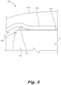
- FIG. 5 is a cross-sectional view of a fluidic die ( 100 ) with a beveled edge ( 108 ) underneath an electrical lead ( 106 ), according to an example of the principles described herein.
- FIG. 5 is a portion of the cross-sectional view taken along the line A-A in FIG. 4
- FIG. 5 also depicts the protrusion ( 312 ) that extends away from a surface of the fluidic die ( 100 ).
- the protrusion ( 312 ) may be formed of an electrically non-conductive polymeric material.
- the protrusion ( 312 ) provides a surface that comes into contact with the electrical lead ( 106 ) before the electrical lead ( 106 ) contacts the surface ( 102 ). Because the protrusion ( 312 ) is formed out of an electrically non-conductive material such as SU-8, contact between the protrusion ( 312 ) and the electrical lead ( 106 ) does not pose a risk of electrical short. Moreover, the polymeric material of the protrusion ( 312 ) is flexible such that it may deform to cushion the electrical lead ( 106 ) in the event of any deflection of the electrical lead ( 106 ). Such cushioning may prevent permanent deformation of the electrical lead ( 106 ). FIG. 5 also depicts that a portion of the electrical lead ( 106 ) that is over the protrusion ( 312 ) curves away from the protrusion.
- FIG. 6 is a flow chart of a method ( 600 ) for forming a fluidic die ( FIG. 1, 100 ) with a beveled edge ( FIG. 1, 108 ) underneath an electrical lead ( FIG. 1, 106 ), according to an example of the principles described herein.
- a fluidic die ( FIG. 1, 100 ) may include a surface ( FIG. 1, 102 ) that is formed of a number of different layers, which include dielectric layers, metallic layers, and oxide layers, among others, each of which serve different purposes in carrying out the operations of a fluidic die ( FIG. 1, 100 ).
- portions of these layers are etched (block 601 ) to form a gap.
- Such an etching also exposes a silicon base layer that is at the bottom of the number of layers.
- This silicon base layer may be a layer in which the nozzles ( FIG. 4, 416 ) of a fluidic die ( FIG. 1, 100 ) are formed.
- a liquid etchant is applied (block 602 ) into the gap to wet etch the silicon base layer.
- liquid etchants examples include tetramethylammonium hydroxide (TMAH) and potassium hydroxide (KOH). These compounds are anisotropic etchants that eat away at the silicon that is not covered by the layers on top of the silicon base layer. This etching process results in a trough in the silicon base layer that has a V-shape. Each wall may have an angle of 54.7 degrees relative to the surface.
- the wet etching used to form the angled trough occurs at the same time as the formation of the fluid channels in the silicon base layer which are fluidly coupled to the nozzles ( FIG.
- fluid is delivered to nozzles ( FIG. 4, 416 ) of a fluidic die ( FIG. 1, 100 ) via fluid channels.
- These fluid channels are formed using a liquid etchant and accordingly can be formed at the same time as the angled trough that will ultimately become a beveled edge ( FIG. 1, 108 ) of the fluidic die ( FIG. 1, 100 ).
- the etching (block 601 ) through the number of layers and applying (block 602 ) of the etchant may be just in that region of the surface ( FIG. 1, 102 ) wherein the bond pads ( FIG. 1, 104 ) are formed.
- the bottom of the angled trough is then cut (block 603 ) to form a fluidic die ( FIG. 1, 100 ) with a beveled edge ( FIG. 1, 108 ). That is, the layer of materials may be used for multiple fluidic dies ( FIG. 1, 100 ), and etching (block 601 ) through a number of layers and applying (block 602 ) a liquid etchant may be done for a number of fluidic dies ( FIG. 1, 100 ) in a single substrate. With such operations completed, each fluidic die ( FIG. 1, 100 ) may be singulated by a saw, which saw when cutting through the angled trough, forms a beveled edge ( FIG. 1, 108 ) on adjacent fluidic dies ( FIG. 1, 100 ).
- FIGS. 7A-7C illustrate the formation of a fluidic die ( FIG. 1, 100 ) with a beveled edge ( FIG. 1, 108 ) underneath an electrical lead ( FIG. 1, 106 ), according to an example of the principles described herein.
- FIG. 7A depicts the etching through of a number of layers of material to form a gap ( 718 ).
- the fluidic die ( FIG. 1, 100 ) may be made up of a number of layers, one of which is a silicon base layer ( 716 ) in which nozzles ( FIG. 4, 416 ) of the fluidic die ( FIG. 1, 100 ) are formed.
- These other layers include any number of film, metallic, oxide, or other layers that carry out different purposes related to the operation of a fluidic die ( FIG. 1, 100 ). Such an etching process exposes a portion of the silicon base layer ( 716 ). Note also, that in this example, the additional layers form a mask for a subsequent liquid etching operation.
- the silicon base layer ( 716 ) is etched away.
- the liquid etchant anisotropically etches the silicon base layer ( 716 ) to form a V-shaped trough with angled walls ( 720 ).
- the angle of these walls ( 720 ) is approximately 54.7 degrees.
- a cut ( 722 ) can then be made to singulate each fluidic die ( FIG. 1, 100 ) as depicted in FIG. 7C . Following the cuts, the angled walls ( 720 ) then form the beveled edges ( 108 ) of the fluidic die.
- using such a fluidic die 1) prevents electrical shorts resulting from contact between a die edge and the electrical leads during manufacturing; 2) improves manufacturing yields; 3) reduces product reliability failures resulting from electrical conductors too close to the grounded die edge; 4) reduces the use for electrical tests to detect shorting, which testing may be destructive, slow, and time-intensive; and 5) reduces beam crash yield loss.
- the devices disclosed herein may address other matters and deficiencies in a number of technical areas.
Landscapes
- Micromachines (AREA)
- Particle Formation And Scattering Control In Inkjet Printers (AREA)
Abstract
Description
Claims (20)
Applications Claiming Priority (1)
| Application Number | Priority Date | Filing Date | Title |
|---|---|---|---|
| PCT/US2018/014788 WO2019147217A1 (en) | 2018-01-23 | 2018-01-23 | Fluidic dies with beveled edges underneath electrical leads |
Publications (2)
| Publication Number | Publication Date |
|---|---|
| US20210170746A1 US20210170746A1 (en) | 2021-06-10 |
| US11225070B2 true US11225070B2 (en) | 2022-01-18 |
Family
ID=67396130
Family Applications (1)
| Application Number | Title | Priority Date | Filing Date |
|---|---|---|---|
| US16/760,923 Expired - Fee Related US11225070B2 (en) | 2018-01-23 | 2018-01-23 | Fluidic dies with beveled edges underneath electrical leads |
Country Status (2)
| Country | Link |
|---|---|
| US (1) | US11225070B2 (en) |
| WO (1) | WO2019147217A1 (en) |
Families Citing this family (2)
| Publication number | Priority date | Publication date | Assignee | Title |
|---|---|---|---|---|
| WO2021096522A1 (en) * | 2019-11-15 | 2021-05-20 | Hewlett-Packard Development Company, L.P. | Fluidic die change of direction detection |
| CN121464047A (en) * | 2023-07-03 | 2026-02-03 | 惠普发展公司,有限责任合伙企业 | Bonding wire for fluid ejection device assembly |
Citations (16)
| Publication number | Priority date | Publication date | Assignee | Title |
|---|---|---|---|---|
| US5519421A (en) * | 1994-07-18 | 1996-05-21 | Hewlett-Packard Company | Disruption of polymer surface of a nozzle member to inhibit adhesive flow |
| US5736998A (en) | 1995-03-06 | 1998-04-07 | Hewlett-Packard Company | Inkjet cartridge design for facilitating the adhesive sealing of a printhead to an ink reservoir |
| US5953034A (en) | 1996-12-18 | 1999-09-14 | Pitney Bowes Inc. | Ink jet transfer printer |
| US6188414B1 (en) | 1998-04-30 | 2001-02-13 | Hewlett-Packard Company | Inkjet printhead with preformed substrate |
| US6331049B1 (en) | 1999-03-12 | 2001-12-18 | Hewlett-Packard Company | Printhead having varied thickness passivation layer and method of making same |
| EP1182037A1 (en) | 2000-08-25 | 2002-02-27 | Hewlett-Packard Company | Printhead die alignment for wide-array inkjet printhead assembly |
| US6402299B1 (en) * | 1999-10-22 | 2002-06-11 | Lexmark International, Inc. | Tape automated bonding circuit for use with an ink jet cartridge assembly in an ink jet printer |
| US6439698B1 (en) * | 2000-01-14 | 2002-08-27 | Lexmark International, Inc | Dual curable encapsulating material |
| US20020122097A1 (en) | 1999-10-29 | 2002-09-05 | Beerling Timothy E. | Electrical interconnect for an inkjet die |
| US6962406B2 (en) | 1999-10-29 | 2005-11-08 | Hewlett-Packard Development Company, L.P. | Fluid ejection device and method of manufacture |
| US20050248629A1 (en) | 2004-05-05 | 2005-11-10 | Bowling Bruce A | Beveled charge structure |
| US20060176338A1 (en) * | 2003-06-27 | 2006-08-10 | Sharp Kabushiki Kaisha | Nozzle plate and method of manufacturing the same |
| EP1415812B1 (en) | 2002-10-30 | 2007-04-25 | Hewlett-Packard Development Company, L.P. | Fluid delivery for printhead assembly |
| US20070279453A1 (en) | 2004-11-19 | 2007-12-06 | Martin De Kegelaer | Method Of Bonding A Nozzle Plate To An Inkjet Printhead |
| US7926916B2 (en) * | 2002-01-31 | 2011-04-19 | Hewlett-Packard Development Company, L.P. | Adhesive joint with an ink trap and method |
| US20140340452A1 (en) * | 2013-05-14 | 2014-11-20 | Stmicroelectronics Asia Pacific Pte. Ltd. | Ink jet printhead with polarity-changing driver for thermal resistors |
-
2018
- 2018-01-23 WO PCT/US2018/014788 patent/WO2019147217A1/en not_active Ceased
- 2018-01-23 US US16/760,923 patent/US11225070B2/en not_active Expired - Fee Related
Patent Citations (16)
| Publication number | Priority date | Publication date | Assignee | Title |
|---|---|---|---|---|
| US5519421A (en) * | 1994-07-18 | 1996-05-21 | Hewlett-Packard Company | Disruption of polymer surface of a nozzle member to inhibit adhesive flow |
| US5736998A (en) | 1995-03-06 | 1998-04-07 | Hewlett-Packard Company | Inkjet cartridge design for facilitating the adhesive sealing of a printhead to an ink reservoir |
| US5953034A (en) | 1996-12-18 | 1999-09-14 | Pitney Bowes Inc. | Ink jet transfer printer |
| US6188414B1 (en) | 1998-04-30 | 2001-02-13 | Hewlett-Packard Company | Inkjet printhead with preformed substrate |
| US6331049B1 (en) | 1999-03-12 | 2001-12-18 | Hewlett-Packard Company | Printhead having varied thickness passivation layer and method of making same |
| US6402299B1 (en) * | 1999-10-22 | 2002-06-11 | Lexmark International, Inc. | Tape automated bonding circuit for use with an ink jet cartridge assembly in an ink jet printer |
| US20020122097A1 (en) | 1999-10-29 | 2002-09-05 | Beerling Timothy E. | Electrical interconnect for an inkjet die |
| US6962406B2 (en) | 1999-10-29 | 2005-11-08 | Hewlett-Packard Development Company, L.P. | Fluid ejection device and method of manufacture |
| US6439698B1 (en) * | 2000-01-14 | 2002-08-27 | Lexmark International, Inc | Dual curable encapsulating material |
| EP1182037A1 (en) | 2000-08-25 | 2002-02-27 | Hewlett-Packard Company | Printhead die alignment for wide-array inkjet printhead assembly |
| US7926916B2 (en) * | 2002-01-31 | 2011-04-19 | Hewlett-Packard Development Company, L.P. | Adhesive joint with an ink trap and method |
| EP1415812B1 (en) | 2002-10-30 | 2007-04-25 | Hewlett-Packard Development Company, L.P. | Fluid delivery for printhead assembly |
| US20060176338A1 (en) * | 2003-06-27 | 2006-08-10 | Sharp Kabushiki Kaisha | Nozzle plate and method of manufacturing the same |
| US20050248629A1 (en) | 2004-05-05 | 2005-11-10 | Bowling Bruce A | Beveled charge structure |
| US20070279453A1 (en) | 2004-11-19 | 2007-12-06 | Martin De Kegelaer | Method Of Bonding A Nozzle Plate To An Inkjet Printhead |
| US20140340452A1 (en) * | 2013-05-14 | 2014-11-20 | Stmicroelectronics Asia Pacific Pte. Ltd. | Ink jet printhead with polarity-changing driver for thermal resistors |
Also Published As
| Publication number | Publication date |
|---|---|
| US20210170746A1 (en) | 2021-06-10 |
| WO2019147217A1 (en) | 2019-08-01 |
Similar Documents
| Publication | Publication Date | Title |
|---|---|---|
| KR100563360B1 (en) | Apparatus and method for using bubble as virtual valve in microinjector to eject fluid | |
| KR100438836B1 (en) | Piezo-electric type inkjet printhead and manufacturing method threrof | |
| US6685302B2 (en) | Flextensional transducer and method of forming a flextensional transducer | |
| US6883903B2 (en) | Flextensional transducer and method of forming flextensional transducer | |
| US6767474B2 (en) | Fluid ejector head having a planar passivation layer | |
| CN105102230B (en) | Fluid ejection apparatus | |
| JP2002254662A (en) | Two processes of trench etching for forming completely integrated thermal ink jet print head | |
| US11225070B2 (en) | Fluidic dies with beveled edges underneath electrical leads | |
| JP2013169749A (en) | Liquid ejecting head, liquid ejecting apparatus and method of manufacturing the liquid ejecting head | |
| KR20030065391A (en) | Substrate and method of forming substrate for fluid ejection device | |
| US11498066B2 (en) | Non-contact liquid printing | |
| US6981759B2 (en) | Substrate and method forming substrate for fluid ejection device | |
| US8348396B2 (en) | Fluid ejection device | |
| EP2332169B1 (en) | Bonding on silicon substrate having a groove | |
| JP2000094700A (en) | Method of manufacturing ink jet recording head and ink jet recording head | |
| US6910758B2 (en) | Substrate and method of forming substrate for fluid ejection device | |
| US11945220B2 (en) | Method and apparatus for dispensing liquid droplets | |
| JP4480956B2 (en) | Discharge device for droplet discharge | |
| JP2000108344A (en) | Ink jet recording device | |
| US12459259B2 (en) | Liquid ejecting head | |
| US8939556B2 (en) | Fluid ejection device | |
| US7686433B2 (en) | Membrane stiffener for electrostatic inkjet actuator | |
| WO2012054021A1 (en) | Method of forming substrate for fluid ejection device | |
| US20120314005A1 (en) | Fluid ejection device | |
| CN104070799A (en) | Insulating substrate electrostatic ink jet print head |
Legal Events
| Date | Code | Title | Description |
|---|---|---|---|
| AS | Assignment |
Owner name: HEWLETT-PACKARD DEVELOPMENT COMPANY, L.P., TEXAS Free format text: ASSIGNMENT OF ASSIGNORS INTEREST;ASSIGNORS:LEIGH, STAN E.;JENSEN, KELLIE SUSANNE;MCMAHON, TERRY;AND OTHERS;SIGNING DATES FROM 20180122 TO 20180123;REEL/FRAME:052544/0834 |
|
| FEPP | Fee payment procedure |
Free format text: ENTITY STATUS SET TO UNDISCOUNTED (ORIGINAL EVENT CODE: BIG.); ENTITY STATUS OF PATENT OWNER: LARGE ENTITY |
|
| STPP | Information on status: patent application and granting procedure in general |
Free format text: NON FINAL ACTION MAILED |
|
| STPP | Information on status: patent application and granting procedure in general |
Free format text: RESPONSE TO NON-FINAL OFFICE ACTION ENTERED AND FORWARDED TO EXAMINER |
|
| STPP | Information on status: patent application and granting procedure in general |
Free format text: NOTICE OF ALLOWANCE MAILED -- APPLICATION RECEIVED IN OFFICE OF PUBLICATIONS |
|
| STPP | Information on status: patent application and granting procedure in general |
Free format text: PUBLICATIONS -- ISSUE FEE PAYMENT VERIFIED |
|
| STCF | Information on status: patent grant |
Free format text: PATENTED CASE |
|
| FEPP | Fee payment procedure |
Free format text: MAINTENANCE FEE REMINDER MAILED (ORIGINAL EVENT CODE: REM.); ENTITY STATUS OF PATENT OWNER: LARGE ENTITY |
|
| LAPS | Lapse for failure to pay maintenance fees |
Free format text: PATENT EXPIRED FOR FAILURE TO PAY MAINTENANCE FEES (ORIGINAL EVENT CODE: EXP.); ENTITY STATUS OF PATENT OWNER: LARGE ENTITY |
|
| STCH | Information on status: patent discontinuation |
Free format text: PATENT EXPIRED DUE TO NONPAYMENT OF MAINTENANCE FEES UNDER 37 CFR 1.362 |
|
| FP | Lapsed due to failure to pay maintenance fee |
Effective date: 20260118 |