US11223425B2 - Optical circuit device, and optical receiver - Google Patents
Optical circuit device, and optical receiver Download PDFInfo
- Publication number
- US11223425B2 US11223425B2 US17/143,720 US202117143720A US11223425B2 US 11223425 B2 US11223425 B2 US 11223425B2 US 202117143720 A US202117143720 A US 202117143720A US 11223425 B2 US11223425 B2 US 11223425B2
- Authority
- US
- United States
- Prior art keywords
- optical
- waveguide
- coupler
- output
- signal
- Prior art date
- Legal status (The legal status is an assumption and is not a legal conclusion. Google has not performed a legal analysis and makes no representation as to the accuracy of the status listed.)
- Active
Links
Images


Classifications
-
- H—ELECTRICITY
- H04—ELECTRIC COMMUNICATION TECHNIQUE
- H04B—TRANSMISSION
- H04B10/00—Transmission systems employing electromagnetic waves other than radio-waves, e.g. infrared, visible or ultraviolet light, or employing corpuscular radiation, e.g. quantum communication
- H04B10/60—Receivers
- H04B10/61—Coherent receivers
- H04B10/613—Coherent receivers including phase diversity, e.g., having in-phase and quadrature branches, as in QPSK coherent receivers
-
- H—ELECTRICITY
- H04—ELECTRIC COMMUNICATION TECHNIQUE
- H04B—TRANSMISSION
- H04B10/00—Transmission systems employing electromagnetic waves other than radio-waves, e.g. infrared, visible or ultraviolet light, or employing corpuscular radiation, e.g. quantum communication
- H04B10/60—Receivers
-
- H—ELECTRICITY
- H04—ELECTRIC COMMUNICATION TECHNIQUE
- H04B—TRANSMISSION
- H04B10/00—Transmission systems employing electromagnetic waves other than radio-waves, e.g. infrared, visible or ultraviolet light, or employing corpuscular radiation, e.g. quantum communication
- H04B10/60—Receivers
- H04B10/61—Coherent receivers
- H04B10/614—Coherent receivers comprising one or more polarization beam splitters, e.g. polarization multiplexed [PolMux] X-PSK coherent receivers, polarization diversity heterodyne coherent receivers
Definitions
- the present disclosure relates to an optical circuit device and an optical receiver.
- coherent optical communication In recent years, high-speed, high-capacity coherent optical communication has been introduced to backbone networks.
- coherent optical communication the amount of data transferred per unit time is increased using two orthogonal phase information, in-phase (hereinafter referred to as “I”) signal and quadrature (hereinafter referred to as “Q”) signal, of the optical electric field.
- I in-phase
- Q quadrature
- a reference light for providing a phase reference at the time of signal reception is mixed with the received signal light to detect and separate the I signal and the Q signal.
- a photonic waveguide device having this coherent detecting function is called a “90-degree optical hybrid”.
- FIG. 1 is a functional diagram of a 90-degree optical hybrid.
- the signal light and the reference light input to the 90-degree optical hybrid are each split into two, and a 90-degree phase difference is given between the two split optical components.
- the components having the same phase as the input lights are I components, and the components having an optical phase shifted by 90 degrees from the input light are Q components.
- the signal light and the reference light, each split into two and provided with a ⁇ /2 phase shift, are mixed, and four optical signals Ip, In, Qp, and Qn whose phases are shifted by 90 degrees respectively are output from the 90-degree optical hybrid.
- the notations “p” and “n” represent complementary outputs.
- the optical signals Ip and In have a 180-degree phase difference, and the optical signals Qp and Qn have a 180-degree phase difference.
- the output ports for Ip, In, Qp, and Qn are connected to the inputs of a photodetector array, and the four optical components are converted into electrical signals. After the photoelectric conversion, a difference between Ip and In and a difference between Qp and Qn are acquired to determine the I signal and the Q signal.
- One conventional technique for implementing a 90-degree optical hybrid by an on-chip photonic waveguide device is to combine a 1 ⁇ 2 coupler with 2 ⁇ 2 couplers. See, for example, U.S. Pat. No. 10,126,498.
- the number of modes used in the combination of the 1 ⁇ 2 coupler and the 2 ⁇ 2 couplers is less than that in a 4 ⁇ 4 multi-mode interferometer (MMI), and influence of the wavelength dependency of inter-mode interference is reduced.
- MMI multi-mode interferometer
- OFI Optical Internetworking Forum
- the four output ports of the 90-degree optical hybrid do not match the layout design of the input ports of the electrical block.
- redundant optical wiring is required, and crosstalk and optical loss will occur.
- the configuration of the digital signal processor (DSP) provided subsequent to the O/E conversion block could be changed.
- DSP digital signal processor
- an optical circuit device has
- a first optical coupler configured to split a first input light into a first output beam and a second output beam with a 90-degree phase difference therebetween
- a second optical coupler configured to split a second input light into a third output beam and a fourth output beam with a 180-degree phase difference therebetween
- a third optical coupler configured to combine one of the first and second output beams of the first optical coupler and one of the third and fourth output beams of the second optical coupler, and output a first optical signal and a second optical signal having a 180-degree phase shift from each other, and
- a fourth optical coupler configured to combine the other of the first and second output beams of the first optical coupler and the other of the third and fourth output beams of the second optical coupler, and output a third optical signal and a fourth optical signal having a 180-degree phase shift from each other.
- FIG. 1 is a functional diagram of a 90-degree optical hybrid
- FIG. 2 is a diagram reconfiguring a known structure of an optical circuit of 90-degree optical hybrid
- FIG. 3 illustrates electric field transfer functions of 2 ⁇ 2 MMIs and a phase-symmetric optical coupler used in FIG. 2 ;
- FIG. 4 is a diagram explaining for a technical issue arising in the configuration of FIG. 2 ;
- FIG. 5 is a schematic diagram of an optical circuit device according to an embodiment
- FIG. 6 is a functional block diagram of an phase inverting coupler used in the optical circuit device of FIG. 5 ;
- FIG. 7 illustrates optical wirings when the optical circuit device of the embodiment is used
- FIG. 8 illustrates a phase difference between an I signal and a Q signal
- FIG. 9A illustrates a configuration example of a phase inverting coupler
- FIG. 9B is a cross-sectional view taken along the I-I′ line of FIG. 9A ;
- FIG. 10A is an electric field simulation diagram presenting propagation states of the phase inverting coupler at position P 0 ;
- FIG. 10B is an electric field simulation diagram presenting propagation states of the phase inverting coupler at position P 6 ;
- FIG. 10C is an electric field simulation diagram presenting propagation states of the phase inverting coupler at position P 8 ;
- FIG. 11 illustrates another configuration example of the phase inverting coupler
- FIG. 12 illustrates a configuration example of a TE 1 generator used in the phase inverting couple of FIG. 11 ;
- FIG. 13 illustrates another example of the TE 1 generator
- FIG. 14 is a diagram explaining for mode conversion in the TE 1 generator of FIG. 13 ;
- FIG. 15 illustrates a modification of the optical circuit device
- FIG. 16 is a schematic diagram of an optical receiver using an optical circuit device, according to an embodiment.
- FIG. 2 to FIG. 4 are diagrams for explaining a technical issue arising in the known structure of 90-degree optical hybrid.
- FIG. 2 reconfigures the optical circuit proposed in the above-described US patent into a simplified form.
- this optical circuit one 1 ⁇ 2 coupler labeled as “C 1 ” and three 2 ⁇ 2 couplers C 2 to C 4 are connected by optical waveguides.
- the 1 ⁇ 2 coupler is a phase-symmetric coupler C 1 formed by a Y-branch optical coupler/splitter.
- phase-symmetric coupler or splitter is defined as “an optical coupler that is configured to split input light into two light signals of substantially same optical phase.”
- a reference light is input to the input port of the phase-symmetric coupler C 1 and split into two light components.
- One light component is connected to one input port of the 2 ⁇ 2 coupler C 2 and the other is connected to one input port of the 2 ⁇ 2 coupler C 3 .
- a signal light is input to one input port of the 2 ⁇ 2 coupler C 4 and split into two signal light beams.
- One of the signal light beams is connected to the other input port of the 2 ⁇ 2 coupler C 2 , and the other is connected to the other input port of the 2 ⁇ 2 coupler C 3 .
- the 2 ⁇ 2 coupler C 2 causes the incident reference light and the incident signal light to interfere with each other, and outputs In and Ip signals from the output ports P 2 and P 3 , respectively.
- the 2 ⁇ 2 coupler C 3 causes the incident reference light and the incident signal light to interfere with each other, and outputs Qn and Qp signals from the output ports P 1 and P 4 , respectively.
- the reference light is expressed as ( ⁇ I LO ) ⁇ e ⁇ circumflex over ( ) ⁇ j( ⁇ LO t ⁇ LO ).
- the signal light is expressed as ( ⁇ I sig ) ⁇ e ⁇ circumflex over ( ) ⁇ j( ⁇ sig t ⁇ sig ).
- I LO and I sig denote the intensities of the reference light and the signal light
- ⁇ LO and ⁇ sig denote the angular frequencies of the reference light and the signal light
- ⁇ LO and ⁇ sig denote the optical phases of the reference light and the signal light.
- FIG. 3 illustrates transfer functions of the electric field of the 2 ⁇ 2 MMI and the phase-symmetric coupler C 1 .
- the phase-symmetric coupler C 1 when a signal normalized to “1” is input, two signals with the same optical phase, each having amplitude 1/ ⁇ 2, are output from the two output ports.
- the outputs from P 1 and P 4 are complementary to each other, for example, Qn is output from P 1 , and Qp is output from P 4 .
- the outputs from P 2 and P 3 are complementary to each other, for example, signal In is output from P 2 , and Ip is output from P 3 .
- the ultimate I signal is represented by (P 3 ⁇ P 2 ), and the ultimate Q signal is represented by (P 4 ⁇ P 1 ).
- a coherent receiver After the optical outputs of Ip, In, Qp, and Qn are converted into electrical signals, the difference between Ip and In and the difference between Qp and Qn are determined.
- the inputs to the electrical block that is, the outputs from photodetectors (PDs) arranged in the order of Ip, In, Qp, and Qn as standardized by the OIF, inconvenience arises in optical wirings.
- PDs photodetectors
- FIG. 4 illustrates a technical issue arising in the configuration of FIG. 2 .
- the optical signal “In” output from the port P 2 of the 2 ⁇ 2 coupler C 2 is connected to PD-In configured to generate an electrical signal for In, and optical signal Ip output from the port P 3 of the 2 ⁇ 2 coupler C 2 is connected to PD-Ip configured to generate an electrical signal for Ip.
- the optical wiring In order to supply the optical signal Ip to PD-Ip, the optical wiring has to bypass the PD array, and the length of the optical wiring is increased. This layout would increase the optical loss.
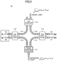
- FIG. 5 is a schematic diagram of an optical circuit device 11 according to an embodiment.
- the optical circuit device 11 has a phase inverting coupler 111 , and 2 ⁇ 2 couplers 112 , 113 and 114 , and serves as a 90-degree optical hybrid overall.
- the optical circuit device 11 uses the phase inverting coupler 111 as an optical splitter that splits the input light into two.
- the “phase inverting coupler” is an optical coupler that splits an input light into two components at a 50/50 split ratio providing a 180-degree phase difference between them.
- FIG. 6 illustrates a function of the phase inverting coupler 111 .
- a light normalized to “1” is input to the phase inverting coupler 111 , the input light is split into two with amplitudes of 1/ ⁇ 2 and ⁇ 1/ ⁇ 2.
- the 1/ ⁇ 2 light is output from one of the two output ports, and ⁇ 1/ ⁇ 2 light is output from the other output port.
- the phase difference between the two output light beams of the phase inverting coupler 111 may not be exactly 180 degrees (i.e., ⁇ radians) and it may include an error of an acceptable range. Because the OIF standardization specification allows an error of 90 degrees ⁇ 7.5 degrees for the phase difference between I and Q signals, the phase difference between the two outputs of the phase inverting coupler 111 may also include an error of 180 ⁇ 7.5 degrees.
- the functions of the 2 ⁇ 2 couplers 112 to 114 are the same as those illustrated in FIG. 3 .
- the phase difference between the output light beams appearing at the bar port and the cross por of the 2 ⁇ 2 couplers 112 to 114 may also include a certain degree of error.
- phase inverting coupler 111 a reference light is input to the phase inverting coupler 111 , and two light beams with a 180-degree phase shift are output.
- One feature of the phase inverting coupler 111 is to provide a 180-degree phase difference between the two split light beams.
- One of the two outputs of the phase inverting coupler 111 is connected to one of the inputs to the 2 ⁇ 2 coupler 112 by an optical waveguide 115 .
- the other output of the phase inverting coupler 111 is connected to one of the inputs to the 2 ⁇ 2 coupler 113 by an optical waveguide 117 .
- a signal light is input to one of the input ports of the 2 ⁇ 2 coupler 114 , and is split into two.
- the 2 ⁇ 2 coupler 114 is an optical splitter with two outputs, between which a 90-degree phase difference is provided as illustrated by the transfer function of FIG. 3 .
- One of the two outputs of the 2 ⁇ 2 coupler 114 is connected to the other input to the 2 ⁇ 2 coupler 112 by an optical waveguide 116 .
- the other output of the 2 ⁇ 2 coupler 114 is connected to the other input to the 2 ⁇ 2 coupler 113 by an optical waveguide 118 .
- the 2 ⁇ 2 coupler 112 is an optical combiner having two input ports and two output ports, and is configured to combine one of the outputs from the 2 ⁇ 2 coupler 114 and one of the outputs from the phase inverting coupler 111 .
- the 2 ⁇ 2 coupler 113 is an optical combiner having two input ports and two output ports, and is configured to combine the other output from the 2 ⁇ 2 coupler 114 and the other output from the phase inverting coupler 111 .
- optical waveguides 115 to 117 connect the phase inverting coupler 111 with the adjacent 2 ⁇ 2 couplers 112 , 113 and 114 do not intersect with each other, excessive loss due to crossing waveguide can be prevented.
- the optical waveguide 115 and the optical waveguide 116 may be of the same length.
- the optical waveguide 117 and the optical waveguide 118 may be of the same length.
- the reference light input to the phase inverting coupler 111 is expressed as ⁇ I LO ⁇ circumflex over ( ) ⁇ j( ⁇ LO t ⁇ LO ), and the signal light input to the 2 ⁇ 2 coupler 114 is expressed as ⁇ I sig ⁇ e ⁇ circumflex over ( ) ⁇ j( ⁇ sig t ⁇ sig ).
- the optical powers at the output ports 81 to 84 are determined based upon the electric field transfer function of FIG. 6 and upon the electric field transfer functions of the 2 ⁇ 2 MMI coupler of FIG. 2 .
- the output powers are expressed by Equation (2).
- the output relationship between P 1 and P 4 is the same as that depicted in FIG. 2 , where Qn is output from P 1 and Qp is output from P 4 .
- the final Q signal is determined by (P 4 ⁇ P 1 ).
- FIG. 7 illustrates optical wirings of the optical circuit device 11 .
- the photodetectors that produce inputs to the electrical block are arranged in the order of PD-Ip, PD-In, PD-Qp, and PD-Qn.
- the port P 2 configured to output the Ip signal is connected by optical wiring 32 to the PD-Ip that produces an electrical signal for Ip.
- the port P 3 configured to output “In” signal is connected by optical wiring 33 to the PD-In that produces an electrical signal for In.
- the port P 4 configured to output a Qp signal is connected by optical wiring 34 to the PD-Qp that produces an electrical signal for Qp.
- the port P 1 configured to output a Qn signal is connected by optical wiring 31 to the PD-Qn that produces an electrical signal for Qn.
- the optical wirings 31 to 34 can connect the output ports P 1 through P 4 of the optical circuit device 11 to the corresponding photodetectors PD at the shortest distance, without bypassing or intersecting.
- the layout design of the optical wirings is simplified, and crosstalk and optical loss are suppressed.
- the size of an optical receiver frontend circuit including the O/E conversion block can be reduced.
- FIG. 8 is a diagram illustrating a phase difference between I and Q signals.
- ⁇ 0 ( ⁇ sig ⁇ LO )t ⁇ ( ⁇ sig ⁇ LO ).
- ⁇ sig and ⁇ LO are the angular frequencies of the signal light and the reference light
- ⁇ sig and ⁇ LO are the optical phases of the signal light and the reference light, respectively.
- the phase inverting coupler 111 used in the optical circuit device 11 may have any configuration as long as the incident light is split into two at a 50/50 split ratio and as long as two light components with a phase difference of about 180 degrees are output. In the following, some examples of the phase inverting coupler 111 will be presented.
- FIG. 9A and FIG. 9B illustrate a phase inverting coupler 111 A, which is an example of the phase inversion coupler 111 .
- FIG. 9A is a plan view
- FIG. 9B is a cross-sectional view taken along the I-I′ line of FIG. 9A .
- the phase inverting coupler 111 A is formed as a directional coupler.
- the phase inverting coupler 111 A has a first waveguide segment WG 1 and a second waveguide segment WG 2 provided parallel with the first waveguide segment WG 1 .
- the first waveguide segment WG 1 and the second waveguide segment WG 2 are positioned close to each other with a gap G 1 between them.
- the waveguide width of the first waveguide segment WG 1 is constant, while the second waveguide segment WG 2 is tapered such that the width continuously varies along the optical axis.
- the position of the cross-section A of the directional coupler is labeled as P 0
- the position of the cross-section B is labeled as P 8
- the distance from the cross-section A to the cross-section B is a taper length.
- the width of the second waveguide segment WG 2 is w 1
- the width of the first waveguide segment WG 1 is w 3 (w 1 >w 3 ).
- the second waveguide segment WG 2 gradually narrows such that the width becomes w 3 at the cross-section B.
- the first waveguide segment WG 1 has a constant width w 3 from the cross-section A to the cross-section B.
- the widths of the first waveguide segment WG 1 and the second waveguide segment WG 2 become the same.
- the first waveguide segment WG 1 and the second waveguide segment WG 2 are formed as waveguide cores made of a high refractive index material on a substrate 201 .
- the waveguide cores are surrounded by a cladding 204 of a low refractive index material.
- the cladding 204 may include an upper+ 203 and a lower cladding 202 made of the same material, or alternatively, the upper cladding 203 may be an air layer.
- the cross-sectional areas of the first waveguide segment WG 1 and the second waveguide segment WG 2 are equal at the cross-section B.
- the first waveguide segment WG 1 is connected to the third waveguide segment WG 3
- the second waveguide segment WG 2 is connected to the fourth waveguide segment WG 4 .
- the waveguide segments WG 3 and WG 4 separate from each other in different directions.
- the cross-sectional areas of the first waveguide segment WG 1 and the second waveguide segment WG 2 become equal to each other, and the light is split into two at a 50/50 split ratio.
- odd-mode light has an antisymmetric field distribution in the width direction (or lateral direction) of the waveguide.
- the phase of the electric field distribution is shifted by ⁇ radians between the first waveguide segment WG 1 and the second waveguide segment WG 2 .
- FIG. 10A to FIG. 10C are simulation results of the electric field distribution of the phase inverting coupler 111 A. Simulation parameters are set as follows.
- the first waveguide segment WG 1 and the second waveguide segment WG 1 are formed of a silicon (Si) core with a height of 220 nm, and the Si core is surrounded by SiO2 clad.
- the width w 1 of the second waveguide segment WG 2 at the cross-section A is 480 nm
- the width w 3 of the second waveguide segment WG 2 at the cross-section B is 400 nm.
- the widths w 3 of the first waveguide segment WG 1 , the third waveguide segment WG 3 , and the fourth waveguide segment WG 4 are all 400 nm.
- the gap G 1 between the first waveguide segment WG 1 and the second waveguide segment WG 2 is 200 nm, and the taper length along the optical axis is 100 ⁇ m.
- the TE odd mode is a propagating mode with the second highest equivalent refractive index among the transverse electric modes in which the main component of the electric field oscillates horizontally with respect to the substrate 201 and in the width direction of the waveguide.
- the mode with the highest equivalent refractive index is the TE even mode.
- the electric field distribution is localized in the first waveguide segment WG 1 having a smaller waveguide size at the cross-section A (namely, at position P 0 ).
- This localized light is equivalent to TE 0 in the case where the waveguide is isolated.
- the width of the waveguide of the second waveguide segment WG 2 gradually approaches the width w 3 of the first waveguide segment WG 1 , and the TE odd mode leaks from the first waveguide segment WG 1 .
- This evanescent light couples to the second waveguide segment WG 2 . Since the width of the second waveguide segment WG 2 varies continuously and slowly, the electric field distribution changes adiabatically while maintaining the continuity.
- An “adiabatic” change in the electric field distribution is a state transition of the propagating mode of incident light to another state, while keeping the same propagating mode, without increasing or decreasing the energy, which occurs when the waveguide configuration changes very slowly.
- the cross-sectional sizes of the first waveguide segment WG 1 and the second waveguide segment WG 2 become the same.
- the electric field of the TE odd mode exists evenly in the first waveguide segment WG 1 and the second waveguide segment WG 2 , and due to the antisymmetric electric field distribution in the TE odd mode, the optical phases between the two waveguides are shifted from each other by 180 degrees.
- the electric field distribution of the second waveguide segment WG 2 is observed as a dark spot because the intensity is represented by a negative sign due to the phase inversion.
- the third waveguide segment WG 3 which extends continuously from the first waveguide segment WG 1
- the fourth waveguide segment WG 4 which extends continuously from the second waveguide segment WG 2 , are gradually separated from each other.
- a phase inverting coupler having two optical outputs whose phases are shifted by n radian from each other is implemented.
- TE mode light is input to the phase inverting coupler 111 A
- TM mode light in which the major component of the electric field oscillates normal to substrate 201 may also be input to the phase inverting coupler 111 A.
- FIG. 11 illustrates a phase inverting coupler 111 B which is another example of the phase inverting coupler 111 .
- the phase inverting coupler 111 B is a combination of a 1 ⁇ 2 coupler 122 and a TE 1 generator 121 .
- the 1 ⁇ 2 coupler 122 may be a 1 ⁇ 2 MMI, a Y-branch coupler, or the like.
- TE 1 when TE 1 is incident on a 1 ⁇ 2 MMI or a Y-branch coupler, two TE 0 modes whose phases are shifted by n radians from each other are output. Making use of this phenomenon, the TE 1 generator 121 is provided on the input side of the 1 ⁇ 2 coupler 122 to supply TE 1 light to the 1 ⁇ 2 coupler. With this structure, incident light of TE 0 or TM 0 can be converted into two phase-inverted TE 0 outputs.
- FIG. 12 illustrates a TE 1 generator 121 A, which is a configuration example of the TE 1 generator 121 used in FIG. 11 .
- the TE 1 generator 121 A converts TE 0 mode light into TE 1 mode light.
- the TE 1 generator 121 A has a first mode converter 80 and a second mode converter 90 .
- the first mode converter 80 has a constant-width waveguide 81 and a tapered waveguide 82 .
- the constant-width waveguide 81 and the tapered waveguide 82 are provided adjacent to each other at a predetermined gap between them.
- the second mode converter 90 has a constant-width waveguide 91 extending continuously from the constant-width waveguide 81 , a constant-width waveguide 92 extending continuously from the tapered waveguide 82 , and a coupling waveguide 93 connecting the constant-width waveguides 91 and 92 .
- the width of the coupling waveguide 93 is preferably set wider than the total of the width of the constant-width waveguide 91 , the width of the constant-width waveguide 92 , and the gap between the two constant-width waveguides 91 and 92 .
- the first mode converter 80 TE 0 light is incident on the constant-width waveguide 81 .
- the width of the tapered waveguide 82 is greater than the width of the constant-width waveguide 81 , and mode coupling rarely occurs between the two waveguides.
- the TE odd mode which has an equivalent refractive index smaller than that of the TE even mode, is localized in the constant-width waveguide 81 with a smaller cross-section.
- the width of the tapered waveguide 82 gradually decreases and approaches the width of the constant-width waveguide 81
- the TE odd mode is gradually coupled to the tapered waveguide 82 .
- the electric field distribution of the TE odd mode existing in the constant-width waveguides 91 and 92 changes to the electric field distribution of the TE 1 mode through the coupling waveguide 93 .
- the electric field distribution in the width direction of the waveguide is represented by an antisymmetric function and has two peaks.
- the TE 1 mode having the second highest equivalent refractive index also has an antisymmetric electric field distribution with two peaks in the width direction. Because of the similarity of the electric field distribution between the TE odd mode and the TE 1 mode, the light entering from the constant-width waveguides 91 and 92 and travelling through the coupling waveguide 93 is converted to the TE 1 mode light. This TE 1 mode light is output from the coupling waveguide 93 .
- FIG. 13 illustrates a TE 1 generator 121 B which is another configuration example of the TE 1 generator.
- the TE 1 generator 121 B converts incident TM 0 light into TE 1 light, and output the TE 1 light.
- TE 1 generator 121 B is formed by a waveguide 130 having a top core 131 and a bottom core 132 .
- the widths of the top core 131 and the bottom core 132 are equal, represented as w 11 .
- the width of the bottom core 132 gradually decreases from w 14 to w 12 .
- the top core 131 and the bottom core 132 have the same width w 12 .
- the width of the top core 131 is different from the width of the bottom core 132 , and the waveguide 130 has an asymmetric shape with respect to the middle plane in the height direction.
- FIG. 14 is a diagram explaining mode conversion in the TE 1 generator 121 B of FIG. 13 .
- the equivalent refractive indexes of TM 0 mode and TE 1 mode are illustrated as a function of position Z along the optical axis of the TE 1 generator 121 B.
- the solid line indicates the second highest equivalent refractive index in the propagating modes of the system of FIG. 13 , and the dashed line indicates the third highest equivalent refractive index.
- the TE 0 mode which has the highest equivalent refractive index, is not illustrated in the figure.
- the equivalent refractive index for TM 0 mode is higher than the equivalent refractive index for TE 1 mode.
- the equivalent refractive index for TE 1 mode is higher than the equivalent refractive index for TM 0 mode.
- the major component of the magnetic field oscillates horizontal to the substrate within the plane perpendicular to the light propagation direction, and change in the equivalent refractive index is small regardless of the Z position.
- the major component of the electric field oscillates horizontal to the substrate within the plane perpendicular to the light propagation direction.
- the propagating mode becomes TM 0 -TE 1 hybrid mode in which almost no individual TM 0 mode or TE 1 mode exists, and higher-order Polarization transformation is performed adiabatically making use of the coupling of TM 0 mode and TE 1 mode.
- This TE 1 generator 121 B is also appropriately used as the TE 1 generator 121 of the phase inverting coupler 111 B.
- FIG. 15 illustrates an optical circuit device 11 A as a modification of the optical circuit device 11 .
- the basic configuration of the optical circuit device 11 A is the same as that of the optical circuit device 11 of FIG. 5 , but a phase shifter 119 is provided in at least one optical waveguide connecting two adjacent optical couplers.
- the phase shifter 119 is, for example, a voltage-driven phase shifter. By controlling the applied voltage, the refractive index of the waveguide is changed to control the propagation speed of light, namely, the optical phase.
- phase shifter 119 is provided on the optical waveguide 118 connecting the 2 ⁇ 2 coupler 113 and the 2 ⁇ 2 coupler 114
- one or more phase shifter(s) may be provided on at least one of the optical waveguides 115 to 118 .
- phase shifter 119 By providing the phase shifter 119 , even when the optical path length of the optical waveguide deviates from the designed value due to manufacturing error or the like, the change in the optical path length is compensated for and the phase difference between the I signal and the Q signal is maintained at or near 90 degrees.
- FIG. 16 illustrates an optical receiver 1 using an optical circuit device 11 of the embodiment.
- the optical receiver 1 has an optical receiver front-end circuit 10 and a signal processing circuit 20 .
- the optical circuit device 11 of the embodiment is applied to 90-degree optical hybrids 11 X and 11 Y (which may be collectively referred to as “90-degree optical hybrid 11 ”) in the optical receiver front-end circuit 10 .
- the optical receiver 1 employs a modulation scheme of, for example, dual-polarization quadrature Phase shift keying (DP-QPSK).
- DP-QPSK dual-polarization quadrature Phase shift keying
- SIGNAL polarization beam splitter
- PBS polarization beam splitter
- the reference light emitted from a local oscillator (labelled as “Lo” in the figure) is split into two by a beam splitter (BS), each guided to a corresponding one of the 90-degree optical hybrid 11 X for X polarization and the 90-degree optical hybrid 11 Y for Y polarization.
- BS beam splitter
- phase inverting coupler 111 is used in each of the 90-degree optical hybrids 11 X and 11 Y.
- the split reference light incident on the corresponding 90-degreen optical hybrid is further split by the phase inverting coupler 111 into two light waves with a 180-degree phase difference between them.
- each of the polarized waves of the signal light is also split by the 2 ⁇ 2 coupler 114 into two light waves with a 90-degree phase difference between them.
- the four split light waves are mixed by the 2 ⁇ 2 couplers 112 and 113 , and four optical signals Ip, In, Qp, and Qn whose phases are shifted by 90 degrees from one another are output.
- the Ip signal and In signal with a 180-degree phase difference are detected by a photodetector set 12 a .
- the photocurrents output from the photodetector set 12 a are converted into voltage signals by the amplifier circuit 13 a which may include a transimpedance amplifier, and the voltage signal is supplied to the signal processing circuit 20 .
- the Qp signal and Qn signal with a 180-degree phase difference are detected by a photodetector set 12 b .
- the photo currents output from the photodetector set 12 b are converted into voltage signals by the amplifier circuit 13 b which may include a transimpedance amplifier, and the voltage signal is supplied to the signal processing circuit 20 .
- the photodetector sets 12 a to 12 d and the amplifier circuits 13 a to 13 d serve as an O/E converter.
- the layout of the four output ports of the 90-degree optical hybrid 11 and the layout of the input ports of O/E converter match each other.
- the length of the optical wirings is minimized.
- the layout of the four output ports of the 90-degree optical hybrid 11 Y matches the layout of the input ports of the O/E converter (including photodetector sets 12 c and 12 d , and amplifier circuits 13 c and 13 d ), and the length of the optical wirings is minimized.
- the analog electrical signals output from the amplifier circuits 13 a to 13 d are digitally sampled by analog-to-digital converters (ADCs) 21 a to 21 d of the signal processing circuit 20 , and are restored, after waveform distortion is compensated for, by the DSP 25 .
- ADCs analog-to-digital converters
- the waveguides and couplers of the optical circuit device 11 may be fabricated using a silicon-on-insulator (SOI) substrate, by forming a Si core using the Si layer and forming a clad using SiO2 of the buried oxide (BOX) layer of the SOI substrate. Because this combination of materials has a great difference in refractive index between the core and the clad, light confinement in the core is strong, and optical loss can be suppressed even with a small radius of curvature of the waveguides.
- SOI silicon-on-insulator
- the configuration of the present disclosure is applicable to a planar lightwave circuit (PLC) formed by etching silica glass provided on a silicon substrate, and to an optical circuit using a compound semiconductor material such as InP or GaAs.
- PLC planar lightwave circuit
Landscapes
- Physics & Mathematics (AREA)
- Electromagnetism (AREA)
- Engineering & Computer Science (AREA)
- Computer Networks & Wireless Communication (AREA)
- Signal Processing (AREA)
- Optical Integrated Circuits (AREA)
- Optical Modulation, Optical Deflection, Nonlinear Optics, Optical Demodulation, Optical Logic Elements (AREA)
Abstract
Description
I=P2−P3=(I sig *I LO)1/2×cos(φ0)
from Equation (2).
Q=P4−P1=(I sig *I LO)1/2×cos(φ0−π/2)
from Equation (2).
Claims (10)
Applications Claiming Priority (3)
| Application Number | Priority Date | Filing Date | Title |
|---|---|---|---|
| JP2020033970A JP7380329B2 (en) | 2020-02-28 | 2020-02-28 | Optical circuit devices and optical receivers |
| JP2020-033970 | 2020-02-28 | ||
| JPJP2020-033970 | 2020-02-28 |
Publications (2)
| Publication Number | Publication Date |
|---|---|
| US20210273730A1 US20210273730A1 (en) | 2021-09-02 |
| US11223425B2 true US11223425B2 (en) | 2022-01-11 |
Family
ID=77463980
Family Applications (1)
| Application Number | Title | Priority Date | Filing Date |
|---|---|---|---|
| US17/143,720 Active US11223425B2 (en) | 2020-02-28 | 2021-01-07 | Optical circuit device, and optical receiver |
Country Status (2)
| Country | Link |
|---|---|
| US (1) | US11223425B2 (en) |
| JP (1) | JP7380329B2 (en) |
Cited By (3)
| Publication number | Priority date | Publication date | Assignee | Title |
|---|---|---|---|---|
| US20220171127A1 (en) * | 2019-04-17 | 2022-06-02 | Nippon Telegraph And Telephone Corporation | Optical 90 Degree Hybrid Circuit |
| US20220244463A1 (en) * | 2020-09-21 | 2022-08-04 | Ii-Vi Delaware, Inc. | Optical couplers and hybrids |
| US20250015897A1 (en) * | 2023-03-09 | 2025-01-09 | Lumentum Technology Uk Limited | Optical coherent receiver having an optical hybrid configuration with reduced phase error |
Families Citing this family (3)
| Publication number | Priority date | Publication date | Assignee | Title |
|---|---|---|---|---|
| JP7380329B2 (en) * | 2020-02-28 | 2023-11-15 | 富士通オプティカルコンポーネンツ株式会社 | Optical circuit devices and optical receivers |
| JP7741384B2 (en) * | 2021-12-28 | 2025-09-18 | 古河ファイテルオプティカルコンポーネンツ株式会社 | Optical 90-degree hybrid |
| CA3263120A1 (en) * | 2022-07-25 | 2024-08-29 | Psiquantum, Corp. | Entanglement generators with incorporated multiplexing |
Citations (15)
| Publication number | Priority date | Publication date | Assignee | Title |
|---|---|---|---|---|
| US3665333A (en) * | 1970-05-05 | 1972-05-23 | Jerrold Electronics Corp | Push-pull amplifier |
| US4887314A (en) * | 1986-10-23 | 1989-12-12 | Plessey Overseas Limited | Optical FSK demodulator |
| JPH0647527A (en) | 1992-07-30 | 1994-02-22 | Nkk Corp | Method and apparatus for mounting upper nozzle for molten metal container |
| US20110229069A1 (en) * | 2010-03-16 | 2011-09-22 | Francesca Bontempi | Planar Waveguide Circuit and Optical Receiver |
| US20130128907A1 (en) * | 2011-11-08 | 2013-05-23 | Optoplex Corporation | Coherent Micro-mixer |
| US20130236172A1 (en) * | 2010-11-18 | 2013-09-12 | Nec Corporation | Coherent optical receiver device and coherent optical receiving method |
| US20140086595A1 (en) * | 2011-05-11 | 2014-03-27 | Nec Corporation | Optical mixer, optical receiver, optical mixing method and production method for optical mixer |
| JP5690902B1 (en) | 2013-10-15 | 2015-03-25 | 株式会社フジクラ | Substrate type optical waveguide device |
| JP5728140B1 (en) | 2013-06-27 | 2015-06-03 | 株式会社フジクラ | High-order polarization conversion element, optical waveguide element, and DP-QPSK modulator |
| US20160274438A1 (en) * | 2013-03-29 | 2016-09-22 | Nec Corporation | Integrated light source and light output control method |
| JP6047527B2 (en) | 2014-08-14 | 2016-12-21 | 株式会社フジクラ | Substrate type optical waveguide device |
| US10126498B1 (en) * | 2017-07-25 | 2018-11-13 | Elenion Technologies, Llc | Optical hybrid |
| US10731383B2 (en) * | 2018-08-01 | 2020-08-04 | Macom Technology Solutions Holdings, Inc. | Symmetric coherent optical mixer |
| US20210273730A1 (en) * | 2020-02-28 | 2021-09-02 | Fujitsu Optical Components Limited | Optical circuit device, and optical receiver |
| US20210294038A1 (en) * | 2020-03-19 | 2021-09-23 | Fujitsu Optical Components Limited | 90-degree optical hybrid |
Family Cites Families (3)
| Publication number | Priority date | Publication date | Assignee | Title |
|---|---|---|---|---|
| US4829598A (en) * | 1987-01-22 | 1989-05-09 | Siemens Aktiengesellschaft | Optical receiver with an optical coupler and an electronic amplifier |
| WO2012086846A1 (en) | 2010-12-21 | 2012-06-28 | 日本電気株式会社 | Optical waveguide device, and manufacturing method for optical waveguide device |
| JP2017142301A (en) | 2016-02-08 | 2017-08-17 | 国立大学法人横浜国立大学 | Strict natural mode multi/demultiplexer and strict natural mode multiplex transmission system |
-
2020
- 2020-02-28 JP JP2020033970A patent/JP7380329B2/en active Active
-
2021
- 2021-01-07 US US17/143,720 patent/US11223425B2/en active Active
Patent Citations (19)
| Publication number | Priority date | Publication date | Assignee | Title |
|---|---|---|---|---|
| US3665333A (en) * | 1970-05-05 | 1972-05-23 | Jerrold Electronics Corp | Push-pull amplifier |
| US4887314A (en) * | 1986-10-23 | 1989-12-12 | Plessey Overseas Limited | Optical FSK demodulator |
| JPH0647527A (en) | 1992-07-30 | 1994-02-22 | Nkk Corp | Method and apparatus for mounting upper nozzle for molten metal container |
| US20110229069A1 (en) * | 2010-03-16 | 2011-09-22 | Francesca Bontempi | Planar Waveguide Circuit and Optical Receiver |
| US20130236172A1 (en) * | 2010-11-18 | 2013-09-12 | Nec Corporation | Coherent optical receiver device and coherent optical receiving method |
| US20140086595A1 (en) * | 2011-05-11 | 2014-03-27 | Nec Corporation | Optical mixer, optical receiver, optical mixing method and production method for optical mixer |
| US20130128907A1 (en) * | 2011-11-08 | 2013-05-23 | Optoplex Corporation | Coherent Micro-mixer |
| US20160274438A1 (en) * | 2013-03-29 | 2016-09-22 | Nec Corporation | Integrated light source and light output control method |
| US20160178841A1 (en) | 2013-06-27 | 2016-06-23 | Fujikura Ltd. | High-order polarization conversion device, optical waveguide device, and dp-qpsk modulator |
| JP5728140B1 (en) | 2013-06-27 | 2015-06-03 | 株式会社フジクラ | High-order polarization conversion element, optical waveguide element, and DP-QPSK modulator |
| US20150104128A1 (en) | 2013-10-15 | 2015-04-16 | Fujikura Ltd. | Planar optical waveguide device and dp-qpsk modulator |
| JP5690902B1 (en) | 2013-10-15 | 2015-03-25 | 株式会社フジクラ | Substrate type optical waveguide device |
| JP6047527B2 (en) | 2014-08-14 | 2016-12-21 | 株式会社フジクラ | Substrate type optical waveguide device |
| US20170139136A1 (en) | 2014-08-14 | 2017-05-18 | Fujikura Ltd. | Planar optical waveguide device, polarization multiplexing 4-value phase modulator, coherent receiver, and polarization diversity |
| US10126498B1 (en) * | 2017-07-25 | 2018-11-13 | Elenion Technologies, Llc | Optical hybrid |
| US20190049665A1 (en) | 2017-07-25 | 2019-02-14 | Elenion Technologies, Llc | Optical Hybrid |
| US10731383B2 (en) * | 2018-08-01 | 2020-08-04 | Macom Technology Solutions Holdings, Inc. | Symmetric coherent optical mixer |
| US20210273730A1 (en) * | 2020-02-28 | 2021-09-02 | Fujitsu Optical Components Limited | Optical circuit device, and optical receiver |
| US20210294038A1 (en) * | 2020-03-19 | 2021-09-23 | Fujitsu Optical Components Limited | 90-degree optical hybrid |
Non-Patent Citations (3)
| Title |
|---|
| "Implementation Agreement for Micro Intradyne Coherent Receivers", OIF, IA #OIF-DPC-MRX-02.0, Retrieved from <URL: https://www.oiforum.com/wp-content/uploads/2019/01/OIF-DPC-MRX-02.0.pdf>, pp. 1-41 (2017) (41 pages). |
| Luhua Xu, et al., "Compact high-performance adiabatic 3-dB coupler enabled by subwavelength grating slot in the silicon-on-insulator platform", Optics Express, vol. 26, No. 23, pp. 29873-29885, (2018) (13 pages). |
| U.S. Appl. No. 10/126,498, filed Nov. 13, 2018, Ma et al. |
Cited By (5)
| Publication number | Priority date | Publication date | Assignee | Title |
|---|---|---|---|---|
| US20220171127A1 (en) * | 2019-04-17 | 2022-06-02 | Nippon Telegraph And Telephone Corporation | Optical 90 Degree Hybrid Circuit |
| US11982839B2 (en) * | 2019-04-17 | 2024-05-14 | Nippon Telegraph And Telephone Corporation | Optical 90 degree hybrid circuit |
| US20220244463A1 (en) * | 2020-09-21 | 2022-08-04 | Ii-Vi Delaware, Inc. | Optical couplers and hybrids |
| US11740411B2 (en) * | 2020-09-21 | 2023-08-29 | Ii-Vi Delaware, Inc. | Optical couplers and hybrids |
| US20250015897A1 (en) * | 2023-03-09 | 2025-01-09 | Lumentum Technology Uk Limited | Optical coherent receiver having an optical hybrid configuration with reduced phase error |
Also Published As
| Publication number | Publication date |
|---|---|
| JP7380329B2 (en) | 2023-11-15 |
| JP2021135460A (en) | 2021-09-13 |
| US20210273730A1 (en) | 2021-09-02 |
Similar Documents
| Publication | Publication Date | Title |
|---|---|---|
| US11223425B2 (en) | Optical circuit device, and optical receiver | |
| US8649643B2 (en) | Optical hybrid circuit and optical receiver | |
| US11402581B2 (en) | Mode converter | |
| JP5966021B2 (en) | Polarization conversion element | |
| US8280256B2 (en) | Optical hybrid circuit, optical receiver and light receiving method | |
| CN103270440B (en) | Optical waveguide device and method for manufacturing optical waveguide device | |
| US12292626B2 (en) | Devices and methods for low voltage optical modulation | |
| US9459406B2 (en) | Polarization beam splitter and optical device | |
| US11333831B2 (en) | Optical couplers and hybrids | |
| US20170099110A1 (en) | Optical receiver circuit and adjustment method for same | |
| Soares et al. | High-performance InP PIC technology development based on a generic photonic integration foundry | |
| JP5598043B2 (en) | 90-degree optical hybrid interferometer and manufacturing method of 90-degree optical hybrid interferometer | |
| JP5640829B2 (en) | Optical hybrid circuit, optical receiver and optical receiving method | |
| US20130243374A1 (en) | Optical branching element, optical waveguide device using optical branching element, and method of manufacturing optical branching element, method of manufacturing optical waveguide device | |
| Li et al. | 800 Gbit/s QSFP-DD transceiver based on thin-film lithium niobate photonic integrated circuit | |
| US20250015897A1 (en) | Optical coherent receiver having an optical hybrid configuration with reduced phase error | |
| US11327234B2 (en) | Optical semiconductor device and reception apparatus | |
| US12487400B2 (en) | Optical device, substrate type optical waveguide element, optical communication apparatus, and inter-waveguide transition method | |
| Villegas et al. | A compact mode controller (switch) using an inverse-designed 2-mode y-junction | |
| US20230208529A1 (en) | Optical 90-degree hybrid | |
| JP2018017808A (en) | Optical waveguide device and optical circuit | |
| Yao | OP I ICA | |
| JPH05158004A (en) | Light modulator | |
| JP2024098873A (en) | Optical device, optical transmitter and optical receiver | |
| Jeong et al. | Compact and wideband optical 90° hybrid based on a one-way tapered MMI coupler |
Legal Events
| Date | Code | Title | Description |
|---|---|---|---|
| AS | Assignment |
Owner name: FUJITSU OPTICAL COMPONENTS LIMITED, JAPAN Free format text: ASSIGNMENT OF ASSIGNORS INTEREST;ASSIGNOR:OKA, AKIRA;REEL/FRAME:054923/0023 Effective date: 20201221 |
|
| FEPP | Fee payment procedure |
Free format text: ENTITY STATUS SET TO UNDISCOUNTED (ORIGINAL EVENT CODE: BIG.); ENTITY STATUS OF PATENT OWNER: LARGE ENTITY |
|
| STPP | Information on status: patent application and granting procedure in general |
Free format text: DOCKETED NEW CASE - READY FOR EXAMINATION |
|
| STPP | Information on status: patent application and granting procedure in general |
Free format text: NOTICE OF ALLOWANCE MAILED -- APPLICATION RECEIVED IN OFFICE OF PUBLICATIONS |
|
| STPP | Information on status: patent application and granting procedure in general |
Free format text: PUBLICATIONS -- ISSUE FEE PAYMENT RECEIVED |
|
| STPP | Information on status: patent application and granting procedure in general |
Free format text: PUBLICATIONS -- ISSUE FEE PAYMENT VERIFIED |
|
| STCF | Information on status: patent grant |
Free format text: PATENTED CASE |
|
| MAFP | Maintenance fee payment |
Free format text: PAYMENT OF MAINTENANCE FEE, 4TH YEAR, LARGE ENTITY (ORIGINAL EVENT CODE: M1551); ENTITY STATUS OF PATENT OWNER: LARGE ENTITY Year of fee payment: 4 |