US11223382B2 - Uplink carrier aggregation device and mobile terminal - Google Patents
Uplink carrier aggregation device and mobile terminal Download PDFInfo
- Publication number
- US11223382B2 US11223382B2 US16/969,239 US201916969239A US11223382B2 US 11223382 B2 US11223382 B2 US 11223382B2 US 201916969239 A US201916969239 A US 201916969239A US 11223382 B2 US11223382 B2 US 11223382B2
- Authority
- US
- United States
- Prior art keywords
- power
- amplifier
- carrier aggregation
- threshold
- uplink carrier
- Prior art date
- Legal status (The legal status is an assumption and is not a legal conclusion. Google has not performed a legal analysis and makes no representation as to the accuracy of the status listed.)
- Active
Links
Images


Classifications
-
- H—ELECTRICITY
- H04—ELECTRIC COMMUNICATION TECHNIQUE
- H04B—TRANSMISSION
- H04B1/00—Details of transmission systems, not covered by a single one of groups H04B3/00 - H04B13/00; Details of transmission systems not characterised by the medium used for transmission
- H04B1/38—Transceivers, i.e. devices in which transmitter and receiver form a structural unit and in which at least one part is used for functions of transmitting and receiving
- H04B1/40—Circuits
-
- H—ELECTRICITY
- H04—ELECTRIC COMMUNICATION TECHNIQUE
- H04L—TRANSMISSION OF DIGITAL INFORMATION, e.g. TELEGRAPHIC COMMUNICATION
- H04L5/00—Arrangements affording multiple use of the transmission path
- H04L5/0001—Arrangements for dividing the transmission path
- H04L5/0003—Two-dimensional division
- H04L5/0005—Time-frequency
- H04L5/0007—Time-frequency the frequencies being orthogonal, e.g. OFDM(A) or DMT
- H04L5/001—Time-frequency the frequencies being orthogonal, e.g. OFDM(A) or DMT the frequencies being arranged in component carriers
-
- H—ELECTRICITY
- H04—ELECTRIC COMMUNICATION TECHNIQUE
- H04B—TRANSMISSION
- H04B1/00—Details of transmission systems, not covered by a single one of groups H04B3/00 - H04B13/00; Details of transmission systems not characterised by the medium used for transmission
- H04B1/005—Details of transmission systems, not covered by a single one of groups H04B3/00 - H04B13/00; Details of transmission systems not characterised by the medium used for transmission adapting radio receivers, transmitters andtransceivers for operation on two or more bands, i.e. frequency ranges
- H04B1/0053—Details of transmission systems, not covered by a single one of groups H04B3/00 - H04B13/00; Details of transmission systems not characterised by the medium used for transmission adapting radio receivers, transmitters andtransceivers for operation on two or more bands, i.e. frequency ranges with common antenna for more than one band
- H04B1/006—Details of transmission systems, not covered by a single one of groups H04B3/00 - H04B13/00; Details of transmission systems not characterised by the medium used for transmission adapting radio receivers, transmitters andtransceivers for operation on two or more bands, i.e. frequency ranges with common antenna for more than one band using switches for selecting the desired band
-
- H—ELECTRICITY
- H04—ELECTRIC COMMUNICATION TECHNIQUE
- H04B—TRANSMISSION
- H04B1/00—Details of transmission systems, not covered by a single one of groups H04B3/00 - H04B13/00; Details of transmission systems not characterised by the medium used for transmission
- H04B1/02—Transmitters
- H04B1/04—Circuits
-
- H—ELECTRICITY
- H04—ELECTRIC COMMUNICATION TECHNIQUE
- H04B—TRANSMISSION
- H04B1/00—Details of transmission systems, not covered by a single one of groups H04B3/00 - H04B13/00; Details of transmission systems not characterised by the medium used for transmission
- H04B1/06—Receivers
- H04B1/16—Circuits
- H04B1/1607—Supply circuits
- H04B1/1615—Switching on; Switching off, e.g. remotely
-
- H—ELECTRICITY
- H04—ELECTRIC COMMUNICATION TECHNIQUE
- H04B—TRANSMISSION
- H04B1/00—Details of transmission systems, not covered by a single one of groups H04B3/00 - H04B13/00; Details of transmission systems not characterised by the medium used for transmission
- H04B1/02—Transmitters
- H04B1/04—Circuits
- H04B2001/0408—Circuits with power amplifiers
Definitions
- the present disclosure relates to the field of communication technology, in particular to an uplink (UL) carrier aggregation (CA) device and a mobile terminal.
- UL uplink
- CA carrier aggregation
- Mobile communication applications such as online video chat, online film and video viewing, and online webcasting, have been ubiquitous in daily life, and accordingly, the requirement on data transfer rate in mobile communication has been increasingly higher.
- the 4 th generation (4G) Long Term Evolution (LTE) carrier aggregation (CA) technology has emerged to satisfy the increasingly higher requirement on data transfer rate.
- the conventional LTE carrier aggregation technologies are categorized into uplink carrier aggregation (ULCA) and downlink carrier aggregation (DLCA), which correspond to transmission and reception by the mobile terminal respectively.
- ULCA uplink carrier aggregation
- DLCA downlink carrier aggregation
- CCs component carriers
- Inter-band uplink CA Inter-band uplink CA (Inter-band ULCA) refers to that a plurality of different channel carriers of different frequency bands are aggregated simultaneously to perform simultaneous transmission.
- PAs power amplifiers
- RF radio frequency
- the present disclosure provides an uplink carrier aggregation device and a mobile terminal, to solve the problem in the related art that the power modules for power amplifiers have a large layout space on the radio frequency printed circuit board.
- the present disclosure solves the technical problem described above by providing the technical solution as follows.
- an uplink carrier aggregation device including: a radio frequency transceiver, at least two power amplifiers, one power-amplifier power module, a control chip, a multiplexer, and an antenna switch.
- the radio frequency transceiver is connected to the at least two power amplifiers and is configured to transmit modulated and transformed first radio frequency signals of different frequency bands to the corresponding power amplifiers.
- the at least two power amplifiers are connected separately to the multiplexer and are configured to amplify the received first radio frequency signals of different frequency bands separately to obtain corresponding second radio frequency signals and transmit the second radio frequency signals to the multiplexer.
- the multiplexer is connected to the antenna switch, and is configured to aggregate the second radio frequency signals transmitted by the at least two power amplifiers and transmit the aggregated second radio frequency signals to the antenna switch.
- the control chip is connected to the radio frequency transceiver and the power-amplifier power module and is configured to determine supply voltage needed by each power amplifier, determine, based on the maximum value of the supply voltages, a target voltage to be output by the power-amplifier power module, and send a power supply instruction to the power-amplifier power module.
- the power-amplifier power module is connected to the at least two power amplifiers, and is configured to regulate the target voltage according to the power supply instruction and output the target voltage to the at least two power amplifiers.
- the present disclosure provides, in some embodiments, a mobile terminal including the uplink carrier aggregation device described above.
- one power-amplifier power module supplies power to at least two power amplifiers, so that the power demand of the at least two power amplifiers can be satisfied, while the layout space of the uplink carrier aggregation device on the radio frequency printed circuit board can be reduced, thereby achieving a better layout of the radio frequency printed circuit board and reduced cost.
- FIG. 1 illustrates a first schematic structural view of an uplink carrier aggregation device according to an embodiment of the present disclosure
- FIG. 2 illustrates a second schematic structural view of an uplink carrier aggregation device according to an embodiment of the present disclosure
- FIG. 3 illustrates a third schematic structural view of an uplink carrier aggregation device according to an embodiment of the present disclosure.
- FIG. 4 illustrates a fourth schematic structural view of an uplink carrier aggregation device according to an embodiment of the present disclosure.
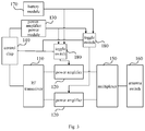
- FIG. 1 a schematic structural view of an uplink carrier aggregation device according to an embodiment of the present disclosure is illustrated.
- the embodiment of the present disclosure provides an uplink carrier aggregation device, including a radio frequency transceiver 110 , at least two power amplifiers 120 , one power-amplifier power module 130 , a control chip 140 , a multiplexer 150 and an antenna switch 160 .
- the radio frequency transceiver 110 is connected to the at least two power amplifiers 120 and is configured to transmit modulated and transformed first radio frequency signals of different frequency bands to corresponding power amplifiers 120 .
- the at least two power amplifiers 120 are connected to the multiplexer 150 , and are configured to amplify the received first radio frequency signals of different frequency bands separately to obtain corresponding second radio frequency signals and transmit the second radio frequency signals to the multiplexer 150 .
- the multiplexer 150 is connected to the antenna switch 160 , and is configured to aggregate the second radio frequency signals transmitted by the at least two power amplifiers 120 and transmit the aggregated second radio frequency signals to the antenna switch 160 .
- the control chip 140 is connected to the radio frequency transceiver 110 and the power-amplifier power module 130 , and is configured to determine supply voltage needed by each power amplifier 120 , determine, based on the maximum value of the supply voltages, a target voltage to be output by the power-amplifier power module 130 , and send a power supply instruction to the power-amplifier power module 130 .
- the power-amplifier power module 130 is connected to the at least two power amplifiers 120 , and is configured to regulate the target voltage according to the power supply instruction and output the target voltage to the at least two power amplifiers 120 .
- the radio frequency transceiver 110 receives and performs modulation and transformation on a low-frequency signal transmitted on frequency-multiplied baseband, to obtain at least two first radio frequency (RF) signals of different frequency bands, and sends the first radio frequency signals to corresponding power amplifiers 120 .
- the first radio frequency signals of different frequency bands are transmitted by the radio frequency transceiver 110 to different power amplifiers respectively.
- the first radio frequency signals of different frequency bands are amplified by the corresponding power amplifiers 120 to obtain corresponding second radio frequency signals that are transmitted to the multiplexer 150 , aggregated by the multiplexer 150 , and then transmitted to the antenna switch 160 , thereby achieving radio frequency signal transmission.
- one power-amplifier power module 130 powers the at least two power amplifiers 120 simultaneously.
- the control chip 140 determines supply voltage needed by each power amplifier 120 based on the transmit power for the frequency band corresponding to each power amplifier 120 , i.e., based on the magnitude of transmit power needed by each power amplifier 120 .
- the supply voltages needed by the different power amplifiers 120 may be the same or different.
- the target voltage to be output by the power-amplifier power module 130 is determined based on the maximum value of the determined supply voltages, and a corresponding power supply instruction is sent to the power-amplifier power module 130 .
- This power supply instruction includes instruction information on the target voltage output from the power-amplifier power module 130 , so that the power-amplifier power module 130 regulates the target voltage according to the power supply instruction and outputs voltages of the same magnitude, i.e. target voltage, to the at least two power amplifiers 120 simultaneously, so as to power the at least two power amplifiers 120 simultaneously.
- the control chip 140 can be configured to determine the maximum value of the determined supply voltages as the target voltage.
- one power-amplifier power module 130 powers the at least two power amplifiers 120 , so that the power demand of the at least two power amplifiers 120 can be satisfied, while the layout space of the uplink carrier aggregation device on the radio frequency printed circuit board can be reduced, thereby achieving a better layout of the radio frequency printed circuit board and reduced cost.
- the uplink carrier aggregation device is mainly applicable to the situation where the at least two power amplifiers 120 have good consistency or transmit at low power, that is, a situation where the power amplifiers 120 operate in a linear zone and have good radio frequency performance and consistency, thereby the supply voltages needed by the at least two power amplifiers 120 are similar.
- the uplink carrier aggregation device includes a radio frequency transceiver 110 , at least two power amplifiers 120 , one power-amplifier power module 130 , a control chip 140 , a multiplexer 150 and an antenna switch 160 .
- the control chip 140 determines, based on the maximum value of the supply voltages, a first target voltage to be output by the power-amplifier power module 130 and sends a power supply instruction to the power-amplifier power module 130 , so that the power-amplifier power module 130 outputs the first target voltage to power the at least two power amplifiers 120 .
- one power-amplifier power module can power the at least two power amplifiers simultaneously, so that the power demand of the at least two power amplifiers can be satisfied, while an excessive layout space of the power-amplifier power module on the radio frequency printed circuit board can be avoided, and consequently the layout space of the uplink carrier aggregation device on the radio frequency printed circuit board can be reduced, thereby achieving a better layout of the radio frequency printed circuit board and reduced cost.
- the at least two power amplifiers 120 may include a first power amplifier 121 and a second power amplifier 122 .
- the control chip 140 is configured to, when two supply voltages are both lower than a first threshold or when the difference between the two supply voltages is lower than a second threshold, determine the maximum value of the two supply voltages as a first target voltage to be output by the power-amplifier power module 130 and sends a power supply instruction to the power-amplifier power module 130 .
- the power-amplifier power module 130 regulates the target voltage according to the power supply instruction, and outputs the first target voltage to the first power amplifier 121 and the second power amplifier 122 .
- the multiplexer 150 may be a quadruplexer 151 .
- the uplink carrier aggregation device may further include a battery module 170 and at least two toggle switches 180 .
- Each of the toggle switches 180 is communicatively connected to the control chip 140 , and each of the toggle switches 180 has a first input end connected to the power-amplifier power module 130 , a second input end connected to the battery module 170 and an output end connected correspondingly to one of the power amplifiers 120 .
- the quantity of provided toggle switches 180 is the same as the quantity of provided power amplifiers 120 . That is, each toggle switch 180 is connected correspondingly to one of the power amplifiers 120 .
- the toggle switches 180 may be single-pole double-throw switches.
- the control chip 140 determines, based on a supply voltage, a second target voltage to be output by the power-amplifier power module 130 , sends a power supply instruction to the power-amplifier power module 130 , and controls the at least two toggle switches 180 to turn on corresponding input ends, so that the battery module 170 powers the power amplifier 120 whose supply voltage is greater than the first threshold, and the power-amplifier power module 130 outputs a second target voltage to power the power amplifier 120 whose supply voltage is lower than or equal to the first threshold.
- the supply voltage used for determining the second target voltage is the maximum value of the supply voltages lower than or equal to the first threshold.
- the control chip 140 determines, based on the maximum value of the supply voltages lower than or equal to the first threshold, a second target voltage to be output by the power-amplifier power module 130 , sends a power supply instruction to the power-amplifier power module 130 , and controls the toggle switch 180 connected correspondingly to the power amplifier 120 whose supply voltage is greater than the first threshold to turn on the second input end, so that the battery module 170 powers the power amplifier 120 whose supply voltage is greater than the first threshold, and controls the toggle switch 180 connected correspondingly to the power amplifier 120 whose supply voltage is lower than or equal to the first threshold to turn on the first input end, so that the
- the battery module 170 of the mobile terminal is directly utilized to power the power amplifier 120 whose supply voltage is greater than the first threshold, and the power-amplifier power module 130 is utilized to power the power amplifier 120 whose supply voltage is lower than or equal to the first threshold, so that the power demand of all the power amplifiers 120 can be satisfied, while an excessive layout space of the power-amplifier power module 130 on the radio frequency printed circuit board can be avoided, and consequently the layout space of the uplink carrier aggregation device on the radio frequency printed circuit board can be reduced, thereby achieving a better layout of the radio frequency printed circuit board and reduced cost.
- the control chip 140 determines, based on the maximum value of the supply voltages, a first target voltage to be output by the power-amplifier power module 130 , sends a power supply instruction to the power-amplifier power module 130 , and controls the at least two toggle switches 180 to turn on the first input ends, so that the power-amplifier power module 130 outputs a first target voltage to power the at least two power amplifiers 120 .
- the control chip 140 determines, based on the maximum value of the supply voltages, the first target voltage to be output, sends a power supply instruction to the power-amplifier power module 130 , and controls the at least two toggle switches 180 to turn on the first input ends, so that the power-amplifier power module 130 outputs the first target voltage to power the power amplifiers 120 whose supply voltages are lower than or equal to the first threshold.
- the battery module 170 does not power the power amplifiers 120 .
- the uplink carrier aggregation device includes a radio frequency transceiver 110 , at least two power amplifiers 120 , one power-amplifier power module 130 , a control chip 140 , a multiplexer 150 and an antenna switch 160 , and further includes a battery module 170 and at least two toggle switches 180 .
- the at least two power amplifiers 120 may include a first power amplifier 121 and a second power amplifier 122 .
- the control chip 140 is configured to, when two supply voltages are both lower than a first threshold or the difference between the two supply voltages is lower than a second threshold, determine the maximum value of the two supply voltages as a first target voltage to be output by the power-amplifier power module 130 , and send a power supply instruction to the power-amplifier power module 130 .
- the power-amplifier power module 130 regulates the target voltage according to the power supply instruction and outputs the first target voltage to the first power amplifier 121 and the second power amplifier 122 .
- the at least two toggle switches 180 may include a first toggle switch 181 and a second toggle switch 182 .
- An output end of the first toggle switch 181 is connected to the first power amplifier 121
- an output end of the second toggle switch 182 is connected to the second power amplifier 122 .
- the control chip 140 determines the supply voltage needed by the second power amplifier as a second target voltage to be output by the power-amplifier power module and controls the second input end of the first toggle switch to be conductive and controls the first input end of the second toggle switch to be conductive.
- the control chip 140 determines the supply voltage needed by the first power amplifier 121 as a second target voltage to be output by the power-amplifier power module 130 , and controls the first input end of the first toggle switch 181 to be conductive and controls the second input end of the second toggle switch 182 to be conductive.
- the battery module 170 of the mobile terminal is directly utilized to power the power amplifier that needs a greater supply voltage, and the power-amplifier power module 130 is utilized to power the power amplifier that needs a lower supply voltage, so that the power demand of the two power amplifiers can be satisfied, while an excessive layout space of the power-amplifier power module 130 on the radio frequency printed circuit board can be avoided, and consequently the layout space of the uplink carrier aggregation device on the radio frequency printed circuit board can be reduced, thereby achieving a better layout of the radio frequency printed circuit board and reduced cost.
- the multiplexer 150 may be a quadruplexer 151 .
- the power-amplifier power module 130 may be an average power tracking module.
- one power-amplifier power module powers at least two power amplifiers, so that the power demand of the at least two power amplifiers can be satisfied, while the layout space of the uplink carrier aggregation device on the radio frequency printed circuit board can be reduced, thereby achieving a better layout of the radio frequency printed circuit board and reduced cost.
- the present disclosure further provides, in an embodiment, a mobile terminal including the uplink carrier aggregation device described above.
- the mobile terminal may be a cellphone, a tablet computer, a laptop computer, a personal digital assistant, or the like.
- the radio frequency printed circuit board can have a better layout and cost is reduced, thereby improving space utilization of the mobile terminal and reducing the design cost of the mobile terminal.
- the terms “installed”, “interconnected”, “connected”, “fixed” “arranged” etc. should be understood in a broad sense, for example, they can mean fixed connection, detachable connection or integration; they can be mechanical connection or electrical connection; they can be direct connection or indirect connection via an intermediate medium, or internal communication between two elements or the interaction between two elements.
- installed can mean fixed connection, detachable connection or integration; they can be mechanical connection or electrical connection; they can be direct connection or indirect connection via an intermediate medium, or internal communication between two elements or the interaction between two elements.
- relational terms such as “first” and “second” are intended merely to distinguish one entity or operation from another entity or operation, and do not necessarily require or imply any such actual relationship or order between these entities or operations.
Landscapes
- Engineering & Computer Science (AREA)
- Signal Processing (AREA)
- Computer Networks & Wireless Communication (AREA)
- Amplifiers (AREA)
- Transceivers (AREA)
Abstract
Description
Claims (15)
Applications Claiming Priority (3)
| Application Number | Priority Date | Filing Date | Title |
|---|---|---|---|
| CN201810145860.2 | 2018-02-12 | ||
| CN201810145860.2A CN108390691B (en) | 2018-02-12 | 2018-02-12 | An uplink carrier aggregation device and mobile terminal |
| PCT/CN2019/073170 WO2019154128A1 (en) | 2018-02-12 | 2019-01-25 | Uplink carrier aggregation device and mobile terminal |
Publications (2)
| Publication Number | Publication Date |
|---|---|
| US20210006280A1 US20210006280A1 (en) | 2021-01-07 |
| US11223382B2 true US11223382B2 (en) | 2022-01-11 |
Family
ID=63068844
Family Applications (1)
| Application Number | Title | Priority Date | Filing Date |
|---|---|---|---|
| US16/969,239 Active US11223382B2 (en) | 2018-02-12 | 2019-01-25 | Uplink carrier aggregation device and mobile terminal |
Country Status (5)
| Country | Link |
|---|---|
| US (1) | US11223382B2 (en) |
| EP (1) | EP3742622B1 (en) |
| CN (1) | CN108390691B (en) |
| ES (1) | ES3032882T3 (en) |
| WO (1) | WO2019154128A1 (en) |
Families Citing this family (6)
| Publication number | Priority date | Publication date | Assignee | Title |
|---|---|---|---|---|
| CN108390691B (en) * | 2018-02-12 | 2019-10-18 | 维沃移动通信有限公司 | An uplink carrier aggregation device and mobile terminal |
| CN109698711B (en) * | 2018-12-18 | 2020-10-30 | 维沃移动通信有限公司 | A radio frequency module and terminal equipment |
| CN110602770A (en) * | 2019-08-22 | 2019-12-20 | 维沃移动通信有限公司 | Power supply management circuit, terminal equipment and power supply management method |
| CN112436861B (en) * | 2020-11-24 | 2022-11-01 | 维沃移动通信有限公司 | Radio frequency circuit, electronic device and control method |
| CN112803764A (en) * | 2020-12-30 | 2021-05-14 | 维沃移动通信有限公司 | Radio frequency system, power supply method of radio frequency system and electronic equipment |
| CN114744606A (en) * | 2022-04-08 | 2022-07-12 | Oppo广东移动通信有限公司 | Power supply system, wireless communication device, and power supply method |
Citations (8)
| Publication number | Priority date | Publication date | Assignee | Title |
|---|---|---|---|---|
| US20110195670A1 (en) * | 2010-02-08 | 2011-08-11 | Sriraman Dakshinamurthy | Method and system for uplink beamforming calibration in a multi-antenna wireless communication system |
| US20110241773A1 (en) | 2010-04-02 | 2011-10-06 | Mks Instruments, Inc. | Multi-Channel Radio Frequency Generator |
| US20120082043A1 (en) | 2010-10-01 | 2012-04-05 | Chien-Hwa Hwang | Indication of user equipment transmit power capacilty in carrier aggregation |
| CN203368478U (en) | 2013-06-07 | 2013-12-25 | 广州埃信电信设备有限公司 | Adaptive digital repeater |
| US20140266429A1 (en) * | 2013-03-13 | 2014-09-18 | Rf Micro Devices, Inc. | Power management/power amplifier operation under dynamic battery drops |
| CN105450189A (en) | 2015-05-26 | 2016-03-30 | 苏州能讯高能半导体有限公司 | Mobile phone transmitting system |
| US20160380652A1 (en) | 2015-06-26 | 2016-12-29 | Skyworks Solutions, Inc. | Power detection of individual carrier of aggregated carrier |
| CN108390691A (en) | 2018-02-12 | 2018-08-10 | 维沃移动通信有限公司 | A kind of up-link carrier polyplant and mobile terminal |
Family Cites Families (4)
| Publication number | Priority date | Publication date | Assignee | Title |
|---|---|---|---|---|
| US8598950B2 (en) * | 2010-12-14 | 2013-12-03 | Skyworks Solutions, Inc. | Apparatus and methods for capacitive load reduction |
| US9220067B2 (en) * | 2011-05-02 | 2015-12-22 | Rf Micro Devices, Inc. | Front end radio architecture (FERA) with power management |
| CN106487415A (en) * | 2016-09-22 | 2017-03-08 | 宇龙计算机通信科技(深圳)有限公司 | A kind of RF front-end circuit and communication terminal |
| CN107070486B (en) * | 2017-05-27 | 2019-08-30 | 青岛海信移动通信技术股份有限公司 | Method and radio frequency circuit for adjusting power supply voltage of radio frequency power amplifier |
-
2018
- 2018-02-12 CN CN201810145860.2A patent/CN108390691B/en active Active
-
2019
- 2019-01-25 EP EP19750595.1A patent/EP3742622B1/en active Active
- 2019-01-25 WO PCT/CN2019/073170 patent/WO2019154128A1/en not_active Ceased
- 2019-01-25 ES ES19750595T patent/ES3032882T3/en active Active
- 2019-01-25 US US16/969,239 patent/US11223382B2/en active Active
Patent Citations (10)
| Publication number | Priority date | Publication date | Assignee | Title |
|---|---|---|---|---|
| US20110195670A1 (en) * | 2010-02-08 | 2011-08-11 | Sriraman Dakshinamurthy | Method and system for uplink beamforming calibration in a multi-antenna wireless communication system |
| US20110241773A1 (en) | 2010-04-02 | 2011-10-06 | Mks Instruments, Inc. | Multi-Channel Radio Frequency Generator |
| CN102725817A (en) | 2010-04-02 | 2012-10-10 | Mks仪器有限公司 | Multi-channel radio frequency generator |
| US20120082043A1 (en) | 2010-10-01 | 2012-04-05 | Chien-Hwa Hwang | Indication of user equipment transmit power capacilty in carrier aggregation |
| US20140266429A1 (en) * | 2013-03-13 | 2014-09-18 | Rf Micro Devices, Inc. | Power management/power amplifier operation under dynamic battery drops |
| CN203368478U (en) | 2013-06-07 | 2013-12-25 | 广州埃信电信设备有限公司 | Adaptive digital repeater |
| CN105450189A (en) | 2015-05-26 | 2016-03-30 | 苏州能讯高能半导体有限公司 | Mobile phone transmitting system |
| US20160380652A1 (en) | 2015-06-26 | 2016-12-29 | Skyworks Solutions, Inc. | Power detection of individual carrier of aggregated carrier |
| CN108390691A (en) | 2018-02-12 | 2018-08-10 | 维沃移动通信有限公司 | A kind of up-link carrier polyplant and mobile terminal |
| US20210006280A1 (en) | 2018-02-12 | 2021-01-07 | Vivo Mobile Communication Co., Ltd. | Uplink carrier aggregation device and mobile terminal |
Non-Patent Citations (2)
| Title |
|---|
| Extended European Search Report dated Feb. 24, 2021 issued in PCT/CN2019/073170. |
| International Preliminary Report on Patentability dated Aug. 27, 2020 issued in PCT/CN2019/073170. |
Also Published As
| Publication number | Publication date |
|---|---|
| ES3032882T3 (en) | 2025-07-28 |
| EP3742622B1 (en) | 2025-05-14 |
| CN108390691A (en) | 2018-08-10 |
| EP3742622A4 (en) | 2021-03-24 |
| EP3742622A1 (en) | 2020-11-25 |
| CN108390691B (en) | 2019-10-18 |
| WO2019154128A1 (en) | 2019-08-15 |
| US20210006280A1 (en) | 2021-01-07 |
Similar Documents
| Publication | Publication Date | Title |
|---|---|---|
| US11223382B2 (en) | Uplink carrier aggregation device and mobile terminal | |
| US10873297B2 (en) | Apparatus and methods for envelope tracking systems with automatic mode selection | |
| US11811371B2 (en) | Radio-frequency circuit and communication device | |
| EP3032739B1 (en) | Envelope tracking in connection with simultaneous transmission in one or more frequency bands | |
| US12500550B2 (en) | Apparatus and methods for biasing of power amplifiers | |
| US20240405726A1 (en) | Power amplifiers with supply capacitor switching | |
| JP6501322B2 (en) | Power amplifier, remote wireless unit, and base station | |
| US20140341318A1 (en) | Average power tracking in a transmitter | |
| US11855328B2 (en) | Remote compensators for mobile devices | |
| US20240079998A1 (en) | Combiners for doherty power amplifier systems | |
| CN104124929A (en) | Apparatus and methods for envelope shaping in power amplifier systems | |
| US8472896B2 (en) | Method and apparatus for transformer power combiner and dynamic power control for outphasing power amplifiers | |
| US20240162860A1 (en) | Power amplifier circuit and power amplification method | |
| US20250357895A1 (en) | Power amplifiers with supply capacitor switching | |
| US20240080005A1 (en) | Doherty power amplifier systems with envelope controlled state | |
| KR20020062409A (en) | Power rate inhancement circuit for rf power amplifier of dual mode mobile phone | |
| US20230063006A1 (en) | Adaptive envelope tracking based on detected transmit signal bandwidth | |
| WO2019119262A1 (en) | Power amplifier and radio frequency device comprising the same | |
| US20240171136A1 (en) | Amplifier assembly with reduced gain variation, front-end module, and mobile device including the same | |
| US20150188501A1 (en) | Power amplifying apparatus | |
| Draxler et al. | A multi-band CMOS Doherty PA with tunable matching network | |
| CN213072652U (en) | RF circuits and electronic equipment | |
| CN114172535B (en) | RF front-end and chips, wireless communication equipment | |
| US20100271997A1 (en) | Apparatus for Dynamically Adjusting a Power Amplifier of a Mobile Terminal | |
| US20250279755A1 (en) | Differential power amplifiers with coupled biasing |
Legal Events
| Date | Code | Title | Description |
|---|---|---|---|
| AS | Assignment |
Owner name: VIVO MOBILE COMMUNICATION CO., LTD., CHINA Free format text: ASSIGNMENT OF ASSIGNORS INTEREST;ASSIGNORS:LI, TIANLIN;LU, ZHIMIN;REEL/FRAME:053467/0484 Effective date: 20200720 |
|
| FEPP | Fee payment procedure |
Free format text: ENTITY STATUS SET TO UNDISCOUNTED (ORIGINAL EVENT CODE: BIG.); ENTITY STATUS OF PATENT OWNER: LARGE ENTITY |
|
| STPP | Information on status: patent application and granting procedure in general |
Free format text: DOCKETED NEW CASE - READY FOR EXAMINATION |
|
| STPP | Information on status: patent application and granting procedure in general |
Free format text: NON FINAL ACTION MAILED |
|
| STPP | Information on status: patent application and granting procedure in general |
Free format text: RESPONSE TO NON-FINAL OFFICE ACTION ENTERED AND FORWARDED TO EXAMINER |
|
| STPP | Information on status: patent application and granting procedure in general |
Free format text: NOTICE OF ALLOWANCE MAILED -- APPLICATION RECEIVED IN OFFICE OF PUBLICATIONS |
|
| STPP | Information on status: patent application and granting procedure in general |
Free format text: PUBLICATIONS -- ISSUE FEE PAYMENT VERIFIED |
|
| STCF | Information on status: patent grant |
Free format text: PATENTED CASE |
|
| MAFP | Maintenance fee payment |
Free format text: PAYMENT OF MAINTENANCE FEE, 4TH YEAR, LARGE ENTITY (ORIGINAL EVENT CODE: M1551); ENTITY STATUS OF PATENT OWNER: LARGE ENTITY Year of fee payment: 4 |
|
| AS | Assignment |
Owner name: NOKIA TECHNOLOGIES OY, FINLAND Free format text: ASSIGNMENT OF ASSIGNORS INTEREST;ASSIGNOR:VIVO MOBILE COMMUNICATION CO., LTD.;REEL/FRAME:073133/0098 Effective date: 20250428 |