US11223295B2 - Capacitor device - Google Patents
Capacitor device Download PDFInfo
- Publication number
- US11223295B2 US11223295B2 US16/564,270 US201916564270A US11223295B2 US 11223295 B2 US11223295 B2 US 11223295B2 US 201916564270 A US201916564270 A US 201916564270A US 11223295 B2 US11223295 B2 US 11223295B2
- Authority
- US
- United States
- Prior art keywords
- capacitor
- case
- fixture
- capacitor case
- fixture member
- Prior art date
- Legal status (The legal status is an assumption and is not a legal conclusion. Google has not performed a legal analysis and makes no representation as to the accuracy of the status listed.)
- Active, expires
Links
Images


Classifications
-
- H—ELECTRICITY
- H01—ELECTRIC ELEMENTS
- H01G—CAPACITORS; CAPACITORS, RECTIFIERS, DETECTORS, SWITCHING DEVICES, LIGHT-SENSITIVE OR TEMPERATURE-SENSITIVE DEVICES OF THE ELECTROLYTIC TYPE
- H01G2/00—Details of capacitors not covered by a single one of groups H01G4/00-H01G11/00
- H01G2/02—Mountings
-
- H—ELECTRICITY
- H01—ELECTRIC ELEMENTS
- H01G—CAPACITORS; CAPACITORS, RECTIFIERS, DETECTORS, SWITCHING DEVICES, LIGHT-SENSITIVE OR TEMPERATURE-SENSITIVE DEVICES OF THE ELECTROLYTIC TYPE
- H01G2/00—Details of capacitors not covered by a single one of groups H01G4/00-H01G11/00
-
- H—ELECTRICITY
- H01—ELECTRIC ELEMENTS
- H01G—CAPACITORS; CAPACITORS, RECTIFIERS, DETECTORS, SWITCHING DEVICES, LIGHT-SENSITIVE OR TEMPERATURE-SENSITIVE DEVICES OF THE ELECTROLYTIC TYPE
- H01G2/00—Details of capacitors not covered by a single one of groups H01G4/00-H01G11/00
- H01G2/10—Housing; Encapsulation
-
- H—ELECTRICITY
- H02—GENERATION; CONVERSION OR DISTRIBUTION OF ELECTRIC POWER
- H02M—APPARATUS FOR CONVERSION BETWEEN AC AND AC, BETWEEN AC AND DC, OR BETWEEN DC AND DC, AND FOR USE WITH MAINS OR SIMILAR POWER SUPPLY SYSTEMS; CONVERSION OF DC OR AC INPUT POWER INTO SURGE OUTPUT POWER; CONTROL OR REGULATION THEREOF
- H02M7/00—Conversion of AC power input into DC power output; Conversion of DC power input into AC power output
- H02M7/003—Constructional details, e.g. physical layout, assembly, wiring or busbar connections
-
- H—ELECTRICITY
- H02—GENERATION; CONVERSION OR DISTRIBUTION OF ELECTRIC POWER
- H02M—APPARATUS FOR CONVERSION BETWEEN AC AND AC, BETWEEN AC AND DC, OR BETWEEN DC AND DC, AND FOR USE WITH MAINS OR SIMILAR POWER SUPPLY SYSTEMS; CONVERSION OF DC OR AC INPUT POWER INTO SURGE OUTPUT POWER; CONTROL OR REGULATION THEREOF
- H02M7/00—Conversion of AC power input into DC power output; Conversion of DC power input into AC power output
- H02M7/006—Conversion of AC power input into DC power output; Conversion of DC power input into AC power output using discharge tubes
-
- H—ELECTRICITY
- H02—GENERATION; CONVERSION OR DISTRIBUTION OF ELECTRIC POWER
- H02M—APPARATUS FOR CONVERSION BETWEEN AC AND AC, BETWEEN AC AND DC, OR BETWEEN DC AND DC, AND FOR USE WITH MAINS OR SIMILAR POWER SUPPLY SYSTEMS; CONVERSION OF DC OR AC INPUT POWER INTO SURGE OUTPUT POWER; CONTROL OR REGULATION THEREOF
- H02M7/00—Conversion of AC power input into DC power output; Conversion of DC power input into AC power output
- H02M7/42—Conversion of DC power input into AC power output without possibility of reversal
- H02M7/44—Conversion of DC power input into AC power output without possibility of reversal by static converters
- H02M7/48—Conversion of DC power input into AC power output without possibility of reversal by static converters using discharge tubes with control electrode or semiconductor devices with control electrode
- H02M7/53—Conversion of DC power input into AC power output without possibility of reversal by static converters using discharge tubes with control electrode or semiconductor devices with control electrode using devices of a triode or transistor type requiring continuous application of a control signal
- H02M7/537—Conversion of DC power input into AC power output without possibility of reversal by static converters using discharge tubes with control electrode or semiconductor devices with control electrode using devices of a triode or transistor type requiring continuous application of a control signal using semiconductor devices only, e.g. single switched pulse inverters
- H02M7/5387—Conversion of DC power input into AC power output without possibility of reversal by static converters using discharge tubes with control electrode or semiconductor devices with control electrode using devices of a triode or transistor type requiring continuous application of a control signal using semiconductor devices only, e.g. single switched pulse inverters in a bridge configuration
-
- H—ELECTRICITY
- H02—GENERATION; CONVERSION OR DISTRIBUTION OF ELECTRIC POWER
- H02M—APPARATUS FOR CONVERSION BETWEEN AC AND AC, BETWEEN AC AND DC, OR BETWEEN DC AND DC, AND FOR USE WITH MAINS OR SIMILAR POWER SUPPLY SYSTEMS; CONVERSION OF DC OR AC INPUT POWER INTO SURGE OUTPUT POWER; CONTROL OR REGULATION THEREOF
- H02M3/00—Conversion of DC power input into DC power output
- H02M3/003—Constructional details, e.g. physical layout, assembly, wiring or busbar connections
-
- H—ELECTRICITY
- H02—GENERATION; CONVERSION OR DISTRIBUTION OF ELECTRIC POWER
- H02M—APPARATUS FOR CONVERSION BETWEEN AC AND AC, BETWEEN AC AND DC, OR BETWEEN DC AND DC, AND FOR USE WITH MAINS OR SIMILAR POWER SUPPLY SYSTEMS; CONVERSION OF DC OR AC INPUT POWER INTO SURGE OUTPUT POWER; CONTROL OR REGULATION THEREOF
- H02M3/00—Conversion of DC power input into DC power output
- H02M3/02—Conversion of DC power input into DC power output without intermediate conversion into AC
- H02M3/04—Conversion of DC power input into DC power output without intermediate conversion into AC by static converters
- H02M3/10—Conversion of DC power input into DC power output without intermediate conversion into AC by static converters using discharge tubes with control electrode or semiconductor devices with control electrode
- H02M3/145—Conversion of DC power input into DC power output without intermediate conversion into AC by static converters using discharge tubes with control electrode or semiconductor devices with control electrode using devices of a triode or transistor type requiring continuous application of a control signal
- H02M3/155—Conversion of DC power input into DC power output without intermediate conversion into AC by static converters using discharge tubes with control electrode or semiconductor devices with control electrode using devices of a triode or transistor type requiring continuous application of a control signal using semiconductor devices only
- H02M3/156—Conversion of DC power input into DC power output without intermediate conversion into AC by static converters using discharge tubes with control electrode or semiconductor devices with control electrode using devices of a triode or transistor type requiring continuous application of a control signal using semiconductor devices only with automatic control of output voltage or current, e.g. switching regulators
- H02M3/158—Conversion of DC power input into DC power output without intermediate conversion into AC by static converters using discharge tubes with control electrode or semiconductor devices with control electrode using devices of a triode or transistor type requiring continuous application of a control signal using semiconductor devices only with automatic control of output voltage or current, e.g. switching regulators including plural semiconductor devices as final control devices for a single load
-
- H—ELECTRICITY
- H02—GENERATION; CONVERSION OR DISTRIBUTION OF ELECTRIC POWER
- H02M—APPARATUS FOR CONVERSION BETWEEN AC AND AC, BETWEEN AC AND DC, OR BETWEEN DC AND DC, AND FOR USE WITH MAINS OR SIMILAR POWER SUPPLY SYSTEMS; CONVERSION OF DC OR AC INPUT POWER INTO SURGE OUTPUT POWER; CONTROL OR REGULATION THEREOF
- H02M7/00—Conversion of AC power input into DC power output; Conversion of DC power input into AC power output
- H02M7/42—Conversion of DC power input into AC power output without possibility of reversal
- H02M7/44—Conversion of DC power input into AC power output without possibility of reversal by static converters
- H02M7/48—Conversion of DC power input into AC power output without possibility of reversal by static converters using discharge tubes with control electrode or semiconductor devices with control electrode
- H02M7/4815—Resonant converters
-
- Y—GENERAL TAGGING OF NEW TECHNOLOGICAL DEVELOPMENTS; GENERAL TAGGING OF CROSS-SECTIONAL TECHNOLOGIES SPANNING OVER SEVERAL SECTIONS OF THE IPC; TECHNICAL SUBJECTS COVERED BY FORMER USPC CROSS-REFERENCE ART COLLECTIONS [XRACs] AND DIGESTS
- Y02—TECHNOLOGIES OR APPLICATIONS FOR MITIGATION OR ADAPTATION AGAINST CLIMATE CHANGE
- Y02B—CLIMATE CHANGE MITIGATION TECHNOLOGIES RELATED TO BUILDINGS, e.g. HOUSING, HOUSE APPLIANCES OR RELATED END-USER APPLICATIONS
- Y02B70/00—Technologies for an efficient end-user side electric power management and consumption
- Y02B70/10—Technologies improving the efficiency by using switched-mode power supplies [SMPS], i.e. efficient power electronics conversion e.g. power factor correction or reduction of losses in power supplies or efficient standby modes
Definitions
- the present invention relates to capacitor devices.
- a known capacitor device constitutes at least part of a power converter installable in vehicles, such as electric vehicles or hybrid vehicles.
- a capacitor device includes a filter capacitor comprised of plural capacitor elements, a smoothing capacitor comprised of plural capacitor elements, and a capacitor case in which the filter capacitor and smoothing capacitor are installed.
- a capacitor device includes a capacitor case that includes at least first, second, and third fixture members for fixation of the capacitor case.
- the third fixture member is located to be separated from a virtual line connecting between a first reference point of the first fixture member and a second reference point of the second fixture member, and located to be closer to the target component than the first and second fixture members are.
- the busbar is located to be closer to the third fixture member than to the virtual line.
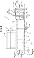
- FIG. 1 is a cross-sectional view of a power converter according to the first embodiment of the present disclosure
- FIG. 2 is a circuit diagram of the power converter illustrated in FIG. 1 ;
- FIG. 3 is an enlarged perspective view of a capacitor device illustrated in FIG. 1 ;
- FIG. 4 is a plan view of the capacitor device illustrated in FIG. 3 when viewed from arrow IV;
- FIG. 5 is a plan view of the capacitor device illustrated in FIG. 3 when viewed from arrow V;
- FIG. 6 is a plan view corresponding to FIG. 5 and schematically illustrating a positional relationship among main and sub fixture members illustrated in FIG. 5 ;
- FIG. 7 is a plan view of a capacitor device according to the second embodiment of the present disclosure, which corresponds to FIG. 6 ;
- FIG. 8 is a plan view of a capacitor device according to the third embodiment of the present disclosure, which corresponds to FIG. 6 .
- a known capacitor device constitutes at least part of a power converter installable in vehicles, such as electric vehicles or hybrid vehicles.
- Such a capacitor device includes a filter capacitor comprised of plural capacitor elements, a smoothing capacitor comprised of plural capacitor elements, and a capacitor case in which the filter capacitor and smoothing capacitor are installed.
- Such a capacitor device includes busbars, i.e. capacitor terminals, for the filter capacitor and smoothing capacitor.
- busbars i.e. capacitor terminals
- Each of the busbars has opposing first and second ends, the first end of each busbar is connected to a corresponding one of the filter capacitor and smoothing capacitor, and the second end of each busbar is drawn out from the capacitor case and extends therefrom.
- the second ends of the respective busbars are electrically connected to semiconductor modules constituting the power converter.
- the busbars drawn out from the capacitor case of the known capacitor device described above are easily subjected to load stress due to vibrations.
- the known capacitor device which is configured such that the capacitors and busbars are integrated with each other, load stress imposed on the busbars may become greater, because the size and weight of the capacitor device becomes greater.
- the present disclosure seeks to provide capacitor devices, each of which is capable of improving resistance of a busbar to vibrations with a simpler structural idea.
- a capacitor device for transferring power between a power source and a target component including an electronic and/or electric component.
- the capacitor device includes at least one capacitor, a capacitor case configured to house the at least one capacitor, and a busbar drawn out from the capacitor case and configured to electrically connect the at least one capacitor to the target component.
- the capacitor case comprises at least first, second, and third fixture members for fixation of the capacitor case.
- the third fixture member is located to be separated from a virtual line connecting between a first reference point of the first fixture member and a second reference point of the second fixture member, and located to be closer to the target component than the first and second fixture members are.
- the busbar is located to be closer to the third fixture member than to the virtual line.
- the third fixture member is located to be separated from the virtual line connecting between the reference points of the respective first and second fixture members, and located to be closer to the target component than the first and second fixture members are.
- capacitor devices which are embodiments of the present disclosure, with reference to the accompanying drawings.
- similar or equivalent parts between the embodiments, to which like reference characters are assigned, are omitted or simplified to avoid redundant description.
- the following describes a power converter 1 , which includes a capacitor device 10 according to the first embodiment of the present disclosure.
- the power converter 1 of the first embodiment is used to be mounted in vehicles, such as electric vehicles or hybrid vehicles.
- the power converter 1 which is installed in a vehicle, serves as an inverter for converting input power supplied from a direct-current (DC) power source into output alternating-current (AC) power required to drive driving wheels of the vehicle.
- DC direct-current
- AC alternating-current
- the power converter 1 includes a semiconductor stack unit, i.e. a semiconductor stack assembly, 3 , a control circuit board 7 , an inductor component 8 , an energization circuit 9 , a capacitor device 10 , a discharge resistor board 24 , and a case, i.e. a housing, 2 .
- These components 3 , 7 , 8 , 10 , and 24 are installed, i.e. housed, in the case 2 .
- the case 2 is made of, for example, a highly heat-dissipative material, such as a metallic material.
- the semiconductor stack unit 3 a plurality of semiconductor modules 4 and a cooling mechanism CM including a set of cooling pipes 6 , an introduction pipe 6 a , and an exhaust pipe 6 b .
- Each semiconductor module 4 incorporates therein a plurality of semiconductor elements 5 (see FIG. 2 ).
- the semiconductor modules 4 include first semiconductor modules 4 A and second semiconductor modules 4 B described later.
- a semiconductor module 4 may serve as an example of a target component such as that recited in the claims of this application.
- the semiconductor stack unit 3 is configured such that the semiconductor modules 4 and the cooling pipes 6 are alternately stacked in a predetermined first direction X, to have a stack structure.
- the cooling pipes 6 include end cooling pipes that respectively constitute both ends of the set of the cooling pipes 6 in the first direction X. That is, each semiconductor module 4 has opposing major sides in the first direction X, and each semiconductor module 4 is sandwiched from the respective major sides by adjacent two cooling pipes 6 respectively located adjacent to the major sides in the first direction X.
- Each of the cooling pipes 6 has a substantially rectangular plate-like shape, and has a longitudinal length in a second direction Y longer than a longitudinal length of each semiconductor module 4 in the second direction Y.
- the first and second directions X and Y can define a third direction, which will be referred to as a height direction, Z perpendicular to the first and second directions X and Y.
- the third direction Z in particular has opposing first and second orientations.
- the first orientation corresponds to an upward direction
- the second orientation corresponds to a downward direction.
- the case 2 has, for example, a substantially rectangular or square parallelepiped shape having opposing top and bottom walls 2 a 1 and 2 a 2 that face each other in the third direction Z and opposing sidewalls 2 b 1 and 2 b 2 facing each other in the second direction Y.
- the case 2 also has unillustrated opposing sidewalls facing each other in the X direction.
- Each of the cooling pipes 6 has opposing first and second ends in its longitudinal direction, i.e. the Y direction; the first end of each cooling pipe 6 is closer to the sidewall 2 b 1 than to the sidewall 2 b 2 , and the second end of each cooling pipe 6 is closer to the sidewall 2 b 2 than to the sidewall 2 b 1 .
- the introduction pipe 6 a is communicably connected to the first end of each cooling pipe 6
- the exhaust pipe 6 b is communicably connected to the second end of each cooling pipe 6 .
- a predetermined refrigerant i.e. a coolant
- the refrigerant flows into all the cooling pipes 6 from their first, and reaches the second ends of all the cooling pipes 6 .
- the refrigerant flows through the exhaust pipe 6 b to be exhausted from the exhaust pipe 6 b . That is, introduction of the refrigerant into the cooling pipes and exhaust of the refrigerant from the cooling pipes 6 are repeatedly carried out, resulting in cooling of the semiconductor modules 4 .
- Each semiconductor module 4 includes a substantially rectangular parallelepiped package (body) having opposing first and second sides in the third direction Z.
- Each semiconductor module 4 includes control terminals 4 a .
- Each of the control terminals 4 a has a first end connected to a corresponding one of the semiconductor elements 5 installed in the corresponding semiconductor module 4 .
- Each of the control terminals 4 a also has a second end, which is opposite to the first end. The second end of each control terminal 4 a is configured to protrude from the first side of the package to extend in the upward orientation of the third direction Z.
- Each semiconductor module 4 also includes a positive DC terminal 4 b , a negative DC terminal 4 b , and an AC terminal 4 d .
- Each of the positive DC, negative DC, and AC terminals 4 b , 4 c , and 4 d has a first end commonly connected to the semiconductor elements 5 installed in the corresponding semiconductor module 4 .
- Each of the positive DC, negative DC, and AC terminals 4 b , 4 c , and 4 d has a second end, which is opposite to the first end.
- the second end of each of the positive DC, negative DC, and AC terminals 4 b , 4 c , and 4 d is configured to protrude from the second side of the package to extend in the downward orientation of the third direction Z.
- the control circuit board 7 is located to face the first side of each of the semiconductor modules 4 , and the second ends of the respective control terminals 4 a are connected to the control circuit board 7 .
- control circuit board 7 controls on-off switching operations of each of the semiconductor elements 5 to thereby convert DC power input to the power converter 1 into AC power.
- a freely available semiconductor switching element typically an insulated-gate bipolar transistor (IGBT) or a metal oxide semiconductor transistor (MOSFET), can be used as each semiconductor element 5 .
- IGBT insulated-gate bipolar transistor
- MOSFET metal oxide semiconductor transistor
- the inductor component 8 which will also be referred to as a reactor component 8 , is located at, for example, the lower side of the semiconductor stack unit 3 to face the semiconductor stack unit 3 in the third direction Z.
- the inductor component 8 includes a coil having opposing first and second ends.
- the energization circuit 9 is connected to a DC power source, i.e. a battery, B having positive and negative terminals Ba and Bb (see FIG. 2 ); the positive terminal Ba of the battery B is connected to the first end of the coil of the inductor component 8 , and the second end of the coil of the inductor component 8 is connected to the first semiconductor modules 4 A.
- the battery B is installed in the vehicle. When energized by the battery B through the energization circuit 9 , the coil of the inductor component 8 generates magnetic flux. That is, the coil of the inductor component 8 is operative to convert electrical energy supplied from the battery B into magnetic energy.
- the capacitor device 10 is configured to supply DC power output from the battery B to the first semiconductor modules 4 A, which serve as electronic and/or electric components.
- the capacitor device 10 is comprised of a filter capacitor 11 and a smoothing capacitor module 12 M including a plurality of smoothing capacitors, in particular two smoothing capacitors, 12 for example connected in parallel to each other.
- the capacitor device 10 is also comprised of a capacitor case 13 . Same types of capacitors can be used for the respective capacitors 10 and 12 .
- the capacitor device 10 is also called a capacitor module or a capacitor assembly. Each of the capacitors 11 has opposing positive and negative electrodes.
- the capacitor case 13 has a bottomed box shape having a top opening surface 14 a , a bottom 14 b opposing the top opening surface 14 a , and a surrounding sidewall 14 c mounted on the bottom 14 b to constitute an enclosure space 14 between the bottom and the surrounding sidewall 14 a .
- each of the top opening surface 14 a and bottom 14 b has a substantially J shape, so that the surrounding sidewall 14 c has a substantially J shape in its lateral cross section parallel to the bottom 14 b.
- the capacitor device 10 includes a plurality of fixture members, such as brackets, 16 each having thin plate-like shape.
- the fixture members 16 are attached to the sidewall 14 c of the capacitor case 13 , so that the capacitor case 13 is fixedly mounted to an inner surface of the case 2 with the fixture members 16 such that the capacitor case 13 is located between the semiconductor stack unit 3 and the sidewall 2 b 2 of the case 2 in the second direction Y.
- Each of the fixture members 16 has a through hole 16 a through which a bolt member 19 serving as a fastening member described below is fitted, and the bolt members 18 are threadably fastened to respective predetermined portions of the case 2 , thus fastening the capacitor case 13 to the case 2 .
- the capacitor case 3 is fixedly mounted to the case 2 at the fixture members 16 .
- the capacitors 11 and 12 are installed in the enclosure space 14 of the capacitor case 13 , and a resin filler, such as a potting resin filler, is filled in the enclosure space 14 of the capacitor case 13 .
- the capacitor case 13 is disposed in the case 2 such that
- the top opening surface 14 a of the capacitor case 13 faces the positive and negative terminals 4 b and 4 c
- a longitudinal direction of the substantially J-shaped capacitor case 13 matches the first direction X
- the substantially J-shaped capacitor case 13 includes a first case portion 13 C 1 having a substantially box shape in which the smoothing capacitors 12 are installed.
- the first case portion 13 C 1 is located to face the positive and negative terminals 4 b and 4 c to be closer to the bottom wall 2 a 2 than to the top wall 2 a 1 .
- the substantially J-shaped capacitor case 13 also includes a second case portion 13 C 2 communicably extending from the first case portion 13 C 1 toward the top wall 2 a 1 of the case 2 .
- Each of the first and second case portions 13 C 1 and 13 C 2 has a predetermined width in the third direction Z, and the width of the first case portion 13 C 1 is longer than the width of the second case portion 13 C 2 .
- the smoothing capacitors 12 are installed in the first case portion 13 C 1
- the filter capacitor 11 is installed in the second case portion 13 C 2 .
- the capacitor device 10 includes a positive busbar 17 and a negative busbar 18 , each of which is configured as a plate member.
- the positive busbar 17 has opposing first and second ends, the first end of the positive busbar 17 is connected to the positive electrodes of the respective capacitors 12 .
- the second end of the positive busbar 17 is drawn out from the resin filler filled in the first capacitor case 13 C 1 of the capacitor case 13 via the top opening surface 14 a , and extends in the second direction Y perpendicular to the top opening surface 14 a toward the positive DC terminal 4 b .
- the second end of the positive busbar 17 is joined to, for example, welded to, the positive DC terminal 4 b.
- the negative busbar 18 has opposing first and second ends, the first end of the negative busbar 18 is connected to the negative electrodes of the respective capacitors 12 .
- the second end of the negative busbar 18 is drawn out from the resin filler filled in the first capacitor case 13 C 1 of the capacitor case 13 via the top opening surface 14 a , and extends in the second direction Y perpendicular to the top opening surface 14 a toward the negative DC terminal 4 c .
- the second end of the negative busbar 18 is joined to, for example, welded to, the negative DC terminal 4 c.
- the discharge resistor board 24 has a substantially rectangular plate-like shape, and includes a discharge resistor 25 for discharging electrical charge stored in the capacitor device 10 .
- the discharge resistor board 24 is electrically connected in parallel to each of the capacitors 11 and 12 , and is located to be non-overlapped with a projected region of the capacitor case 13 on an X-Z plane perpendicular to the second direction Y.
- the sidewall 14 c of the capacitor case 13 has opposing first and second sidewall portions 14 c 1 and 14 c 2 , and the sidewall 14 c is located in the case 2 such that the first sidewall portion 14 c 1 faces the top wall 2 a 1 of the case 2 , and the second sidewall portion 14 c 2 faces the bottom wall 2 a 2 of the case 2 .
- the first sidewall portion 14 c 1 has a flat sidewall portion extending in the first direction X.
- the capacitor device 10 includes a board support member 15 , which has, for example, a rectangular board-like shape, extending from the first sidewall portion 14 c 1 of the sidewall 14 toward the top wall 2 a 1 of the case 2 in the Z direction.
- the discharge resistor board 24 is mounted to the board support member 15 . This prevents thermal interference between the discharge resistor 25 , which serves as an electric heating element, and the capacitors 11 and 12 .
- the discharge resistor board 24 is located to extend from the first sidewall portion 14 c 1 of the sidewall 14 toward the top wall 2 a 1 of the case 2 along the top opening surface 14 a of the capacitor case 13 . Because the potting resin filler is filled in the capacitor case 13 , the top opening surface 14 a of the capacitor case 13 can also be called a potting surface.
- the capacitor device 10 includes voltage detection terminals 26 for measuring a voltage across each of the filter capacitor 11 and the smoothing capacitors 12 .
- Each of the voltage detection terminals 26 are disposed to extend from the board support member 15 mounted to the first sidewall portion 14 c 1 of the sidewall 14 in the third direction Z toward the control circuit board 7 . That is, the voltage detection terminals 26 are configured to project from the first sidewall portion 14 c 1 of the sidewall 14 of the capacitor case 13 so as to be arranged between the discharge resistor board 24 and the control circuit board 7 . This configuration prevents the voltage detection terminals 26 from being adversely affected by electromagnetic noise generated from the capacitors 11 and 12 .
- the following describes the whole structure of the power converter 1 , and the structure of each selected component of the power converter 1 in detail.
- control circuit board 7 is configured to control on-off switching operations of each of the semiconductor elements 5 to thereby convert DC power output from the battery B input to the power converter 1 into AC power.
- the number of the semiconductor modules 4 is set to 8, and each of the semiconductor modules 4 is comprised of
- a first semiconductor element 5 comprised of an upper-arm semiconductor switch, such as an IGBT, and a flyback diode connected in antiparallel thereto
- a second semiconductor element 5 comprised of a lower-arm semiconductor switch, such as an IGBT, and a flyback diode connected in antiparallel thereto; the first and second semiconductor elements 5 are connected in series to each other
- the eight semiconductor modules 4 include
- the first group of semiconductor modules 4 A which serves as a part of a voltage booster 31 of an inverter circuit 30
- the inductor component 8 , filter capacitor 11 , and semiconductor modules 4 A serve as the voltage booster 31 .
- control circuit board 7 is configured to control on-off switching operations of each semiconductor switch included in the semiconductor modules 4 A to thereby enable the voltage booster 31 to boost the DC voltage across the battery B.
- the filter capacitor 11 is operative to eliminate noise current component included in a direct current based on the DC voltage inputted from the battery B via a pair of voltage input terminals 20 .
- the filter capacitor 11 is located electrically upstream of the smoothing capacitors 12 with respect to the battery B.
- the smoothing capacitors 12 and semiconductor modules 4 B serve as the power converter 32 of the inverter circuit 30 .
- the semiconductor modules 4 B also is divided into a first set of semiconductor modules 4 B for a first three-phase (U-, V-, and W-phase) AC motor-generator MG 1 , and a second group of semiconductor modules 4 B for a second three-phase AC motor-generator MG 2 . That is, the AC terminals 4 d of the respective semiconductor modules 4 B of the first group are connected to the first three-phase AC motor-generator MG 1 . Similarly, the AC terminals 4 d of the respective semiconductor modules 4 B of the second group are connected to the second three-phase AC motor-generator MG 2 .
- control circuit board 7 is configured to control
- the smoothing capacitors 12 are operative to smooth the DC voltage boosted by the voltage booster 31 .
- the discharge resistor 25 which is electrically connected in parallel to each of the capacitors 11 and 12 , is operative to discharge electrical internal charge stored in each of the capacitors 11 and 12 while, for example, the power converter 1 is stopped.
- the J-shaped capacitor case 13 of the capacitor device 10 which is located such that the longitudinal direction matches the first direction X, includes the smoothing capacitors 12 and the filter capacitor 11 are installed to be aligned in the first direction X.
- the pair of power input terminals 20 includes a positive terminal 20 p and a negative terminal 20 n
- the pair of power supply terminals 21 include a positive terminal 21 p and a negative terminal 21 n.
- the capacitor device 10 includes a bent plate-like positive busbar 22 mounted to the second case portion 13 C 2 of the capacitor case 13 and connected to the positive electrode of the filter capacitor 11 .
- the positive busbar 22 has opposing first and second ends 22 a and 22 b that respectively serve as the positive terminal 20 p of the pair of power input terminals 20 , and the positive terminal 21 p of the pair of power supply terminals 21 .
- the capacitor device 10 includes a bent plate-like negative busbar 23 mounted to the second case portion 13 C 2 of the capacitor case 13 and connected to the negative electrode of the filter capacitor 11 .
- the negative busbar 23 has opposing first and second ends 23 a and 23 b that respectively serve as the negative terminal 20 n of the pair of power input terminals 20 , and the negative terminal 21 n of the pair of power supply terminals 21 .
- a middle portion of the negative busbar 21 between the first and second ends 23 a and 23 b is embedded in the potting resin filler filled in the second case portion 13 C 2 .
- the positive and negative terminals 20 p and 20 n of the pair of power input terminals 20 are connected to the respective positive and negative terminals Ba and Bb of the battery B, and are also connected to the respective positive and negative terminals 21 p and 21 n of the pair of power supply terminals 21 .
- the positive terminal 21 p of the pair of power supply terminals 21 is connected to the first end of the coil of the inductor component 8 , and the second end of the coil of the inductor component 8 is connected to the connection point between each of the upper- and lower-arm switches of each of the first semiconductor modules 4 A.
- the negative terminal 21 n of the pair of power supply terminals 21 is connected to the lower-arm semiconductor switches of the respective first and second semiconductor modules 4 A and 4 B.
- This configuration enables the DC voltage across the battery B is input to the filter capacitor 11 , and the direct current based on the DC voltage is input to the coil of the inductor component 8 .
- the pair of power input terminals 20 and pair of power supply terminals 21 are located to be closer to the filter capacitor 11 than to the smoothing capacitors 12 .
- the capacitor device 10 includes the plurality of fixture members 16 .
- the plurality of fixture members 16 include three fixture members 16 A, 16 B, and 16 C.
- the fixture members 16 A, 16 B, and 16 C are provided to the capacitor case 13 and are fixedly mounted to the case 2 , so that the capacitor case 13 is fixedly mounted to the case 2 .
- the bolt members 19 which have been fitted through the respective through holes 16 a of the fixture members 16 , threadably fastened to respective predetermined portions of the case 2 , thus fastening the capacitor case 13 to the case 2 .
- the fixture members 16 A and 16 B which respectively serve as main fixture members, are respectively mounted to first and second longitudinal ends E 1 and E 2 of the case 13 in the first direction X, i.e. the longitudinal direction thereof.
- the remaining fixture member 16 C which serves as a sub fixture member, is mounted to a middle portion of the capacitor case 13 and located between the main fixture members 16 A and 16 B.
- the main fixture members 16 A and 16 B have substantially the same height in the third direction Z as viewed from the second direction Y that is a normal direction to the top opening surface 14 a of the enclosure space 14 .
- the sub fixture member 16 C has a height in the third direction Z, which is different from the substantially mutually equal height of the main fixture members 16 A and 16 B in the third direction Z.
- the sub fixture member 16 C is located to be higher than the main fixture members 16 A and 16 B in the third direction, i.e. height direction, Z.
- the sub fixture member 16 C is located to be separated, i.e. deviated, from the virtual line L, and located to be closer to the semiconductor modules 4 than the main fixture members 16 A and 16 B are. That is, the virtual line L extends in the first direction X.
- the top opening surface 14 a overlaps the virtual line L when viewed from the normal line to the top opening surface 14 a , that is, the second direction Y.
- the width of the virtual line L in the third direction Z is set to be sufficiently smaller than the thickness of each fixture member 16 A, 16 B, and 16 C.
- the positive and negative busbars 17 and 18 are located to be closer to the sub fixture member 16 c than to the virtual line L. That is, when a region of the capacitor case 13 is divided into a first region S and a second region SX with respect to the virtual line L as viewed from the second direction Y, the positive and negative busbars 17 and 18 are located to the first region S in the capacitor case 13 . Because the first region S is closer to the sub fixture member 16 C than the second region SX is, the first region S serves as a vibration resistance region S.
- the first region S i.e. the vibration resistance region S, is suitable for the busbars 17 and 18 to be electrically connected to the semiconductor modules 4 .
- the three virtual lines L, M, and N constitute a triangular region Sa surrounded by the three virtual lines L, M, and N.
- the first region S i.e. the vibration resistance region S
- the first region S is more resistant to, i.e. is less subjected to, load stress due to vibrations.
- Locating the busbars 17 and 18 to the capacitor case to be closer to the sub fixture member 16 C than to the virtual line L suppresses load stress received by the busbars 17 and 18 to be a lower level, resulting in the busbars 17 and 18 having an improved resistance to vibrations.
- busbars 17 and 18 locating the busbars 17 and 18 to the vibration resistance region S in the capacitor case 13 suppresses load stress received by the busbars 17 and 18 to be a lower level, resulting in the busbars 17 and 18 having an improved resistance to vibrations.
- the above configuration of the capacitor device 10 maintains load stress received by the busbars 17 and 18 to be a lower level.
- the capacitor device 10 is designed based on a simpler structural idea that the busbars 17 and 18 are located to the region S defined by the three fixture members 16 A, 16 B, and 16 C.
- the capacitor device 10 has an even more superior structure that, when a projected surface of the capacitor case 13 on an X-Z plane perpendicular to the second direction Y is viewed from the second direction Y, a center of gravity G of the projected surface, i.e. the top opening surface 14 a of the capacitor case 13 , is located to be within the triangular region Sa.
- This configuration results in the capacitor device 10 having a higher effect of suppressing vibrations of the capacitor device 10 as compared with another capacitor device whose center of gravity of the projected surface is located outside the triangular region Sa. This therefore results in more reduction in load stress received by the busbars 17 and 18 .
- a position of the sub fixture member 16 C of the capacitor device 10 in the first direction X according to the first embodiment is located between a position of the capacitor 11 in the first direction X and a position of the capacitor 12 in the first direction X; the capacitors 11 and 12 are adjacent to each other.
- the following describes the second embodiment of the present disclosure with reference to FIG. 7 .
- the configuration and functions of a capacitor device 110 according to the second embodiment are mainly different from those of the capacitor device 10 according to the first embodiment by the following points. The following therefore mainly describes the different points.
- the main fixture members 16 A, 16 B, and 16 C according to the second embodiment respectively have different heights in the third direction Z as viewed from the second direction Y. That is, the sub fixture member 16 C is located to be higher than the main fixture member 16 B in the height direction Z, and the main fixture member 16 B is located to be higher than the main fixture member 16 A in the height direction Z.
- This configuration results in the virtual line L is inclined with respect to the first direction X.
- the second embodiment obtains the same effects as those obtained by the first embodiment.
- the following describes the third embodiment of the present disclosure with reference to FIG. 8 .
- the configuration and functions of a capacitor device 210 according to the third embodiment are mainly different from those of the capacitor device 10 according to the first embodiment by the following points. The following therefore mainly describes the different points.
- the capacitor device 10 includes the plurality of fixture members 16 .
- the plurality of fixture members 16 include fourth fixture members 16 A, 16 B, 16 C, and 16 D.
- the fixture members 16 A, 16 B, 16 C, and 16 D are provided to the capacitor case 13 and are fixedly mounted to the case 2 , so that the capacitor case 13 is fixedly mounted to the case 2 .
- the main fixture members 16 A and 16 B are respectively mounted to the first and second longitudinal ends E 1 and E 2 of the case 13 in the first direction X, i.e. the longitudinal direction thereof.
- the remaining fixture members 16 C and 16 D which serve as respective sub fixture members, are mounted to the middle portion of the capacitor case 13 and located between the main fixture members 16 A and 16 B.
- the main fixture members 16 A and 16 B have substantially the same height in the third direction Z as viewed from the second direction Y.
- the sub fixture members 16 C and 16 D each have a height in the third direction Z, which is higher than the substantially same height of the main fixture members 16 A and 16 B in the third direction Z.
- Each of the sub fixture members 16 C and 16 D is located to be separated, i.e. deviated, from the virtual line L, and located to be closer to the semiconductor modules 4 than the main fixture members 16 A and 16 B are.
- the sub fixture member 16 C is located to be closer to the semiconductor modules 4 than the sub fixture member 16 D is.
- the capacitor case 13 has the first region S and the second region SX partitioned by the virtual line L.
- the first region S serves as the vibration resistance region S.
- the first region S i.e. the vibration resistance region S, is suitable for the busbars 17 and 18 to be electrically connected to the semiconductor modules 4 .
- the third embodiment obtains the same effects as those obtained by the first embodiment.
- the first and second main fixture members 16 A and 16 B can be different in height in the third direction Z.
- five or more fixture members can be provided to the capacitor case 13 and can be fixedly mounted to the case 2 , so that the capacitor case 13 can be fixedly mounted to the case 2 .
- the center of gravity G of the projected surface, i.e. the top opening surface 14 a of the capacitor case 13 , of the corresponding one of the capacitor devices 10 , 110 , and 210 is located to be within the triangular region Sa, but can be located outside the triangular region Sa.
- the capacitor device 10 is configured to supply the DC power output from the battery B to the semiconductor modules 4 of the inverter circuit 30 , but can be configured to transfer power between a power source and a target component including an electronic and/or electric component.
Landscapes
- Engineering & Computer Science (AREA)
- Power Engineering (AREA)
- Microelectronics & Electronic Packaging (AREA)
- Inverter Devices (AREA)
- Fixed Capacitors And Capacitor Manufacturing Machines (AREA)
- Mounting Of Printed Circuit Boards And The Like (AREA)
Abstract
Description
Claims (6)
Applications Claiming Priority (3)
| Application Number | Priority Date | Filing Date | Title |
|---|---|---|---|
| JPJP2018-171535 | 2018-09-13 | ||
| JP2018171535A JP2020043732A (en) | 2018-09-13 | 2018-09-13 | Capacitor device |
| JP2018-171535 | 2018-09-13 |
Publications (2)
| Publication Number | Publication Date |
|---|---|
| US20200091833A1 US20200091833A1 (en) | 2020-03-19 |
| US11223295B2 true US11223295B2 (en) | 2022-01-11 |
Family
ID=69773407
Family Applications (1)
| Application Number | Title | Priority Date | Filing Date |
|---|---|---|---|
| US16/564,270 Active 2039-11-07 US11223295B2 (en) | 2018-09-13 | 2019-09-09 | Capacitor device |
Country Status (3)
| Country | Link |
|---|---|
| US (1) | US11223295B2 (en) |
| JP (1) | JP2020043732A (en) |
| CN (1) | CN110895990B (en) |
Families Citing this family (2)
| Publication number | Priority date | Publication date | Assignee | Title |
|---|---|---|---|---|
| JP7003964B2 (en) * | 2019-04-05 | 2022-01-21 | 株式会社デンソー | Power converter |
| CN113765460B (en) * | 2020-06-04 | 2025-01-14 | 比亚迪股份有限公司 | Integrated capacitors, motor controllers and vehicles |
Citations (3)
| Publication number | Priority date | Publication date | Assignee | Title |
|---|---|---|---|---|
| JP2014045035A (en) | 2012-08-24 | 2014-03-13 | Denso Corp | Capacitor device |
| US20150256096A1 (en) | 2012-10-09 | 2015-09-10 | Hitachi Automotive Systems, Ltd. | Capacitor Module and Power Conversion Device |
| US20170347485A1 (en) * | 2015-01-26 | 2017-11-30 | Hitachi Automotive Systems, Ltd. | Power Conversion Device |
Family Cites Families (6)
| Publication number | Priority date | Publication date | Assignee | Title |
|---|---|---|---|---|
| JP5403089B2 (en) * | 2011-05-26 | 2014-01-29 | 株式会社デンソー | Power converter |
| JP5862528B2 (en) * | 2012-09-25 | 2016-02-16 | 株式会社デンソー | Power converter |
| JP6383614B2 (en) * | 2014-09-08 | 2018-08-29 | 京セラ株式会社 | Capacitor module and power unit |
| JP2016092086A (en) * | 2014-10-31 | 2016-05-23 | 日立オートモティブシステムズ株式会社 | Case structure |
| KR101807243B1 (en) * | 2015-09-21 | 2017-12-11 | 주식회사 뉴인텍 | 3 Step Vacuum Metallizing Coating Film Capacitor, and Inverter system |
| JP6521850B2 (en) * | 2015-12-08 | 2019-05-29 | 三菱重工サーマルシステムズ株式会社 | Capacitor unit and power converter |
-
2018
- 2018-09-13 JP JP2018171535A patent/JP2020043732A/en active Pending
-
2019
- 2019-09-09 US US16/564,270 patent/US11223295B2/en active Active
- 2019-09-11 CN CN201910856369.5A patent/CN110895990B/en active Active
Patent Citations (3)
| Publication number | Priority date | Publication date | Assignee | Title |
|---|---|---|---|---|
| JP2014045035A (en) | 2012-08-24 | 2014-03-13 | Denso Corp | Capacitor device |
| US20150256096A1 (en) | 2012-10-09 | 2015-09-10 | Hitachi Automotive Systems, Ltd. | Capacitor Module and Power Conversion Device |
| US20170347485A1 (en) * | 2015-01-26 | 2017-11-30 | Hitachi Automotive Systems, Ltd. | Power Conversion Device |
Also Published As
| Publication number | Publication date |
|---|---|
| CN110895990A (en) | 2020-03-20 |
| CN110895990B (en) | 2024-01-23 |
| US20200091833A1 (en) | 2020-03-19 |
| JP2020043732A (en) | 2020-03-19 |
Similar Documents
| Publication | Publication Date | Title |
|---|---|---|
| US9425707B2 (en) | Inverter device capable of appropriately fixing a power module having a switching element and a smoothing capacitor in a limited region | |
| JP5550927B2 (en) | Power converter | |
| US8406026B2 (en) | Power conversion apparatus | |
| US20180358903A1 (en) | Power converter | |
| JP6648859B2 (en) | Power converter | |
| JP6646739B2 (en) | Power converter | |
| RU2651950C2 (en) | Electrical power control unit | |
| JP7052531B2 (en) | Power converter | |
| US9693476B2 (en) | Power conversion apparatus | |
| US11588423B2 (en) | Electric-power conversion apparatus | |
| JP2020150724A (en) | Power converter | |
| US11223295B2 (en) | Capacitor device | |
| US10615707B2 (en) | Inverter control device | |
| JP5964715B2 (en) | Electrical equipment case and power control unit | |
| JP7167328B2 (en) | power converter | |
| JP2016116306A (en) | Power converter for electric vehicle | |
| JP2016100986A (en) | Power converter for electric vehicles | |
| JP2008092695A (en) | Connecting conductor and inverter device | |
| JP2020162226A (en) | Power conversion unit | |
| JP5919424B1 (en) | Capacitor module | |
| JP7294247B2 (en) | electric unit | |
| JP7746910B2 (en) | Electrical Equipment | |
| JP2025035913A (en) | Power Conversion Equipment | |
| JP2021180541A (en) | Power conversion device | |
| CA3060965A1 (en) | High density low inductance power inverter |
Legal Events
| Date | Code | Title | Description |
|---|---|---|---|
| FEPP | Fee payment procedure |
Free format text: ENTITY STATUS SET TO UNDISCOUNTED (ORIGINAL EVENT CODE: BIG.); ENTITY STATUS OF PATENT OWNER: LARGE ENTITY |
|
| AS | Assignment |
Owner name: DENSO CORPORATION, JAPAN Free format text: ASSIGNMENT OF ASSIGNORS INTEREST;ASSIGNORS:SANO, TOMOHISA;HARADA, DAISUKE;ARAKI, SEIDO;AND OTHERS;SIGNING DATES FROM 20190930 TO 20191028;REEL/FRAME:051010/0116 |
|
| STPP | Information on status: patent application and granting procedure in general |
Free format text: NON FINAL ACTION MAILED |
|
| STPP | Information on status: patent application and granting procedure in general |
Free format text: RESPONSE TO NON-FINAL OFFICE ACTION ENTERED AND FORWARDED TO EXAMINER |
|
| STPP | Information on status: patent application and granting procedure in general |
Free format text: NOTICE OF ALLOWANCE MAILED -- APPLICATION RECEIVED IN OFFICE OF PUBLICATIONS |
|
| STPP | Information on status: patent application and granting procedure in general |
Free format text: PUBLICATIONS -- ISSUE FEE PAYMENT RECEIVED |
|
| STPP | Information on status: patent application and granting procedure in general |
Free format text: AWAITING TC RESP, ISSUE FEE PAYMENT VERIFIED |
|
| STPP | Information on status: patent application and granting procedure in general |
Free format text: PUBLICATIONS -- ISSUE FEE PAYMENT VERIFIED |
|
| STCF | Information on status: patent grant |
Free format text: PATENTED CASE |
|
| MAFP | Maintenance fee payment |
Free format text: PAYMENT OF MAINTENANCE FEE, 4TH YEAR, LARGE ENTITY (ORIGINAL EVENT CODE: M1551); ENTITY STATUS OF PATENT OWNER: LARGE ENTITY Year of fee payment: 4 |