US11223136B2 - Feed circuit for antenna of angle of arrival measurement system - Google Patents
Feed circuit for antenna of angle of arrival measurement system Download PDFInfo
- Publication number
- US11223136B2 US11223136B2 US16/871,351 US202016871351A US11223136B2 US 11223136 B2 US11223136 B2 US 11223136B2 US 202016871351 A US202016871351 A US 202016871351A US 11223136 B2 US11223136 B2 US 11223136B2
- Authority
- US
- United States
- Prior art keywords
- antenna
- coupler
- signal
- conductive element
- conductive elements
- Prior art date
- Legal status (The legal status is an assumption and is not a legal conclusion. Google has not performed a legal analysis and makes no representation as to the accuracy of the status listed.)
- Active, expires
Links
Images


Classifications
-
- H—ELECTRICITY
- H01—ELECTRIC ELEMENTS
- H01Q—ANTENNAS, i.e. RADIO AERIALS
- H01Q1/00—Details of, or arrangements associated with, antennas
- H01Q1/27—Adaptation for use in or on movable bodies
- H01Q1/32—Adaptation for use in or on road or rail vehicles
- H01Q1/325—Adaptation for use in or on road or rail vehicles characterised by the location of the antenna on the vehicle
- H01Q1/3275—Adaptation for use in or on road or rail vehicles characterised by the location of the antenna on the vehicle mounted on a horizontal surface of the vehicle, e.g. on roof, hood, trunk
-
- H—ELECTRICITY
- H01—ELECTRIC ELEMENTS
- H01Q—ANTENNAS, i.e. RADIO AERIALS
- H01Q11/00—Electrically-long antennas having dimensions more than twice the shortest operating wavelength and consisting of conductive active radiating elements
- H01Q11/02—Non-resonant antennas, e.g. travelling-wave antenna
- H01Q11/08—Helical antennas
-
- G—PHYSICS
- G01—MEASURING; TESTING
- G01S—RADIO DIRECTION-FINDING; RADIO NAVIGATION; DETERMINING DISTANCE OR VELOCITY BY USE OF RADIO WAVES; LOCATING OR PRESENCE-DETECTING BY USE OF THE REFLECTION OR RERADIATION OF RADIO WAVES; ANALOGOUS ARRANGEMENTS USING OTHER WAVES
- G01S3/00—Direction-finders for determining the direction from which infrasonic, sonic, ultrasonic or electromagnetic waves, or particle emission, not having a directional significance, are being received
- G01S3/02—Direction-finders for determining the direction from which infrasonic, sonic, ultrasonic or electromagnetic waves, or particle emission, not having a directional significance, are being received using radio waves
- G01S3/023—Monitoring or calibrating
-
- G—PHYSICS
- G01—MEASURING; TESTING
- G01S—RADIO DIRECTION-FINDING; RADIO NAVIGATION; DETERMINING DISTANCE OR VELOCITY BY USE OF RADIO WAVES; LOCATING OR PRESENCE-DETECTING BY USE OF THE REFLECTION OR RERADIATION OF RADIO WAVES; ANALOGOUS ARRANGEMENTS USING OTHER WAVES
- G01S3/00—Direction-finders for determining the direction from which infrasonic, sonic, ultrasonic or electromagnetic waves, or particle emission, not having a directional significance, are being received
- G01S3/02—Direction-finders for determining the direction from which infrasonic, sonic, ultrasonic or electromagnetic waves, or particle emission, not having a directional significance, are being received using radio waves
- G01S3/14—Systems for determining direction or deviation from predetermined direction
- G01S3/46—Systems for determining direction or deviation from predetermined direction using antennas spaced apart and measuring phase or time difference between signals therefrom, i.e. path-difference systems
- G01S3/48—Systems for determining direction or deviation from predetermined direction using antennas spaced apart and measuring phase or time difference between signals therefrom, i.e. path-difference systems the waves arriving at the antennas being continuous or intermittent and the phase difference of signals derived therefrom being measured
-
- G—PHYSICS
- G07—CHECKING-DEVICES
- G07C—TIME OR ATTENDANCE REGISTERS; REGISTERING OR INDICATING THE WORKING OF MACHINES; GENERATING RANDOM NUMBERS; VOTING OR LOTTERY APPARATUS; ARRANGEMENTS, SYSTEMS OR APPARATUS FOR CHECKING NOT PROVIDED FOR ELSEWHERE
- G07C9/00—Individual registration on entry or exit
- G07C9/00174—Electronically operated locks; Circuits therefor; Nonmechanical keys therefor, e.g. passive or active electrical keys or other data carriers without mechanical keys
- G07C9/00309—Electronically operated locks; Circuits therefor; Nonmechanical keys therefor, e.g. passive or active electrical keys or other data carriers without mechanical keys operated with bidirectional data transmission between data carrier and locks
-
- H—ELECTRICITY
- H01—ELECTRIC ELEMENTS
- H01Q—ANTENNAS, i.e. RADIO AERIALS
- H01Q1/00—Details of, or arrangements associated with, antennas
- H01Q1/36—Structural form of radiating elements, e.g. cone, spiral, umbrella; Particular materials used therewith
- H01Q1/38—Structural form of radiating elements, e.g. cone, spiral, umbrella; Particular materials used therewith formed by a conductive layer on an insulating support
-
- H—ELECTRICITY
- H01—ELECTRIC ELEMENTS
- H01Q—ANTENNAS, i.e. RADIO AERIALS
- H01Q21/00—Antenna arrays or systems
- H01Q21/0006—Particular feeding systems
-
- H—ELECTRICITY
- H01—ELECTRIC ELEMENTS
- H01Q—ANTENNAS, i.e. RADIO AERIALS
- H01Q21/00—Antenna arrays or systems
- H01Q21/06—Arrays of individually energised antenna units similarly polarised and spaced apart
- H01Q21/08—Arrays of individually energised antenna units similarly polarised and spaced apart the units being spaced along or adjacent to a rectilinear path
-
- H—ELECTRICITY
- H01—ELECTRIC ELEMENTS
- H01Q—ANTENNAS, i.e. RADIO AERIALS
- H01Q21/00—Antenna arrays or systems
- H01Q21/06—Arrays of individually energised antenna units similarly polarised and spaced apart
- H01Q21/22—Antenna units of the array energised non-uniformly in amplitude or phase, e.g. tapered array or binomial array
-
- H—ELECTRICITY
- H01—ELECTRIC ELEMENTS
- H01Q—ANTENNAS, i.e. RADIO AERIALS
- H01Q21/00—Antenna arrays or systems
- H01Q21/24—Combinations of antenna units polarised in different directions for transmitting or receiving circularly and elliptically polarised waves or waves linearly polarised in any direction
-
- G—PHYSICS
- G01—MEASURING; TESTING
- G01S—RADIO DIRECTION-FINDING; RADIO NAVIGATION; DETERMINING DISTANCE OR VELOCITY BY USE OF RADIO WAVES; LOCATING OR PRESENCE-DETECTING BY USE OF THE REFLECTION OR RERADIATION OF RADIO WAVES; ANALOGOUS ARRANGEMENTS USING OTHER WAVES
- G01S2205/00—Position-fixing by co-ordinating two or more direction or position line determinations; Position-fixing by co-ordinating two or more distance determinations
- G01S2205/01—Position-fixing by co-ordinating two or more direction or position line determinations; Position-fixing by co-ordinating two or more distance determinations specially adapted for specific applications
-
- G—PHYSICS
- G01—MEASURING; TESTING
- G01S—RADIO DIRECTION-FINDING; RADIO NAVIGATION; DETERMINING DISTANCE OR VELOCITY BY USE OF RADIO WAVES; LOCATING OR PRESENCE-DETECTING BY USE OF THE REFLECTION OR RERADIATION OF RADIO WAVES; ANALOGOUS ARRANGEMENTS USING OTHER WAVES
- G01S5/00—Position-fixing by co-ordinating two or more direction or position line determinations; Position-fixing by co-ordinating two or more distance determinations
- G01S5/02—Position-fixing by co-ordinating two or more direction or position line determinations; Position-fixing by co-ordinating two or more distance determinations using radio waves
- G01S5/0284—Relative positioning
-
- G—PHYSICS
- G07—CHECKING-DEVICES
- G07C—TIME OR ATTENDANCE REGISTERS; REGISTERING OR INDICATING THE WORKING OF MACHINES; GENERATING RANDOM NUMBERS; VOTING OR LOTTERY APPARATUS; ARRANGEMENTS, SYSTEMS OR APPARATUS FOR CHECKING NOT PROVIDED FOR ELSEWHERE
- G07C9/00—Individual registration on entry or exit
- G07C9/00174—Electronically operated locks; Circuits therefor; Nonmechanical keys therefor, e.g. passive or active electrical keys or other data carriers without mechanical keys
- G07C2009/00753—Electronically operated locks; Circuits therefor; Nonmechanical keys therefor, e.g. passive or active electrical keys or other data carriers without mechanical keys operated by active electrical keys
- G07C2009/00769—Electronically operated locks; Circuits therefor; Nonmechanical keys therefor, e.g. passive or active electrical keys or other data carriers without mechanical keys operated by active electrical keys with data transmission performed by wireless means
- G07C2009/00793—Electronically operated locks; Circuits therefor; Nonmechanical keys therefor, e.g. passive or active electrical keys or other data carriers without mechanical keys operated by active electrical keys with data transmission performed by wireless means by Hertzian waves
Definitions
- the present disclosure relates to angle of arrival measurement systems including circular polarized and/or linear antennas.
- PEPS passive entry/passive start
- ECU vehicle's central PEPS electronic control unit
- the user in possession of the key fob may unlock and enter the vehicle by grabbing the door handle.
- the user in possession of the key fob may activate a vehicle function by pushing a button on the key fob.
- the central PEPS ECU authenticates the key fob to determine if the key fob is authorized to access the vehicle and uses the signal strength obtained by a plurality of sensors to estimate the distance between the key fob and the vehicle and the location of the key fob relative to the vehicle. If the key fob is authenticated and is located within an authorizing zone, the PEPS system makes the corresponding vehicle function available to the user (i.e., the vehicle is started).
- LF systems use proprietary grade radio protocols using low frequency (LF) signals of approximately 125 kHz.
- LF systems were implemented by conventional PEPS systems because the wave propagation enables relatively accurate estimation of a distance between the key fob and the vehicle and the location of the key fob relative to the vehicle by using signal strengths within a target activation range of, for example, 2 meters.
- LF signals due to the extremely long wavelength of the LF signal relative to the size of a vehicle antenna and key fob receiver, it is difficult to reliably communicate with a key fob using LF systems beyond a few meters within reasonable power consumption and safe transmit power levels. As such, it is difficult to make any of the vehicle's functions available to the user when the key fob is located more than a few meters away from the vehicle.
- smart devices such as smartphones and wearable devices, wherein the smart devices are able to communicate at a range greater than the activation range of LF systems, such as 100 meters.
- smart devices enable the availability of various vehicle functions and long range distancing features, such as passive welcome lighting, distance bounding on remote parking applications, etc.
- antenna systems of current PEPS systems may prevent the PEPS system from accurately estimating RSSI power, distances and angles for RSSI power, differential RSSI power, trilateration measurements, triangulation measurements, and correlation finger printing locationing values for signal transmission between the key fob and the vehicle.
- Antenna systems of current PEPS system may also prevent the PEPS system from accurately estimating the location of the key fob relative to the vehicle.
- a feed circuit for feeding an antenna includes: a first coupler including a first pair of opposing conductive elements; a second coupler including a second pair of opposing conductive elements; a third coupler including a third pair of opposing conductive elements; a delay line; first terminals configured to connect to the antenna; second terminals connected to a ground reference; and a feed terminal connected to the first coupler and configured to receive at least one of a transmit signal to be transmitted from the antenna or a combined received signal from the antenna.
- the first terminals are connected to the second coupler and the third coupler and configured to output a signal at different phases to conductive elements of the antenna.
- the second terminals are connected to the first coupler, the second coupler and the third coupler.
- the delay line extends from the first coupler to the third coupler.
- the feed terminal is configured to receive the transmit signal to be transmitted from the antenna.
- Each of the first coupler, the second coupler, the third coupler and the delay line phase shift the transmit signal by 90°.
- the first opposing pair of conductive elements includes a first conductive element disposed over a second conductive element.
- the second opposing pair of conductive elements includes a third conductive element disposed over a fourth conductive element.
- the third opposing pair of conductive elements includes a fifth conductive element disposed over a sixth conductive element.
- a width of the first conductive element is smaller than a width of the second conductive element.
- a width of the third conductive element is smaller than a width of the fourth conductive element.
- a width of the fifth conductive element is smaller than a width of the sixth conductive element.
- a shape of the first conductive element matches a shape of the second conductive element.
- a shape of the third conductive element matches a shape of the fourth conductive element.
- a shape of the fifth conductive element matches a shape of the sixth conductive element.
- only one conductive element extends between the feed terminal and one of the first terminals.
- the first opposing pair of conductive elements include a first conductive element and a second conductive element.
- the second opposing pair of conductive elements includes a third conductive element and a fourth conductive element.
- the second conductive element is connected to the feed terminal.
- Fourth conductive element is connected to one of the second terminals.
- the first conductive element and the third conductive element are integrally formed as a single conductive element, which extends between the feed terminal and the one of the second terminals.
- the second conductive element and the fourth conductive element do not extend between the feed terminal and the one of the second terminals.
- an angle-of-arrival measurement system includes: the feed circuit; the antenna; and a control module configured to determine an angle-of-arrival of the received signal.
- a perimeter of the feed circuit is smaller than a perimeter of the antenna.
- the antenna is a quadrifilar helix antenna.
- the quadrifilar helix antenna includes conductive elements connected respectively to the first terminals.
- a feed circuit for an antenna includes: a component layer including resistors, where the resistors are connected to a ground reference; a first ground layer disposed on the component layer; a first signal layer disposed on the first ground layer and including a feed terminal, first conductive elements and a delay line, where one of the first conductive elements is connected to one of the resistors; a second signal layer disposed on the first signal layer and including second conductive elements, where first ones of the second conductive elements are connected to some of the resistors; a second ground layer disposed on the second signal layer; and an antenna mounting layer including first terminals configured to connect to the antenna and configured to transmit via the antenna phase shifted versions of a signal received at the feed terminal. The first terminals are configured to connect to some of the first conductive elements and second ones of the second conductive elements.
- two of the second conductive elements are connected to two of the resistors.
- the first ground layer transfers signals of components in the component layer.
- the second ground layer isolates the antenna from the first signal layer and the second signal layer.
- widths of the first conductive elements are wider than widths of the second conductive elements.
- first conductive elements and the second conductive elements provide a first coupler, a second coupler, and a third coupler.
- the first coupler, the second coupler, the third coupler, and the delay line phase shift a transmit signal by 90°.
- the feed circuit further includes vias connecting the terminals to the some of the first conductive elements and second ones of the second conductive elements.
- second terminals are connected to one of the first conductive elements and two of the second conductive elements. Vias connect the second terminals respectively to the resistors.
- FIG. 1 is an illustration of a portable device and a vehicle implementing one or more feed circuits in accordance with an embodiment of the present disclosure.
- FIG. 2 is a functional block diagram of a portable device and a vehicle implementing one or more feed circuits in accordance with an embodiment of the present disclosure.
- FIG. 3 is a functional block diagram of a sensor of a vehicle implementing feed circuits in accordance with an embodiment of the present disclosure.
- FIG. 4 is a functional block diagram of a communication gateway of a vehicle implementing feed circuits according to the present disclosure.
- FIG. 5 is an illustration of an example antenna system in accordance with an embodiment of the present disclosure.
- FIGS. 6A-6B are illustrations of an example antenna assembly (or antenna) of the antenna system in accordance with an embodiment of the present disclosure.
- FIGS. 7A-7D are illustrations of an example antenna including multiple antenna elements in accordance with an embodiment of the present disclosure.
- FIGS. 8-9 are illustrations of another example antenna including antenna elements in accordance with an embodiment of the present disclosure.
- FIGS. 10-12 are illustrations of an encasing element of an antenna in accordance with an embodiment of the present disclosure.
- FIGS. 13-14 are illustrations of an antenna in accordance with an embodiment of the present disclosure.
- FIG. 15 illustrates a portion of a printed circuit board including a portion of an antenna mounted on the printed circuit board in accordance with an embodiment of the present disclosure.
- FIGS. 16A-16B is an illustration of another example angle of arrival measurement system in accordance with an embodiment of the present disclosure.
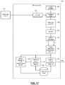
- FIG. 17 is a functional block diagram of an example microcontroller in accordance with an embodiment of the present disclosure.
- FIGS. 18-20 are flowcharts of example control algorithms in accordance with an embodiment of the present disclosure.
- FIG. 21 is a phase angle vs. time plot provided as an example unwrapping and aligning of phase angle points for phase angle difference determinations in accordance with an embodiment of the present disclosure.
- FIG. 22 is a phase angle difference vs azimuth angle plot illustrating differences in phase for an outer pair of antennas in accordance with an embodiment of the present disclosure.
- FIG. 23 is a phase angle difference vs azimuth angle plot illustrating differences in phase for an inner pair of antennas in accordance with an embodiment of the present disclosure.
- FIG. 24 is illustrates a method of determining angle of arrival in accordance with an embodiment of the present disclosure.
- FIG. 25 is a functional block diagram of an example receiving circuit for determining a phase angle between in-phase and quadrature components of a radio frequency signal in accordance with an embodiment of the present disclosure.
- FIG. 26 is a top view of an example feed circuit implemented according to an embodiment of the present disclosure.
- FIG. 27 is a cross-sectional view of a portion of the feed circuit of FIG. 26 illustrating example via connections according to an embodiment of the present disclosure.
- FIG. 28 is an end cross-sectional view of an example coupler according to an embodiment of the present disclosure.
- FIG. 29 is a top view of a top portion of the feed circuit of FIG. 26 illustrating top conductive elements of couplers of the feed circuit.
- FIG. 30 is a top view of a bottom portion of the feed circuit of FIG. 26 illustrating bottom conductive elements of the couplers and delay line of the feed circuit.
- FIG. 31 is a functional block diagram representation of the feed circuit of FIG. 26 .
- An angle-of-arrival (AOA) measurement system includes an AOA antenna that has a set of circular polarized antennas and/or a set of linear polarized antennas.
- the AOA antenna requires phase adjustments for corresponding conductive feed lines to satisfy radiation performance and phase sensitivity accuracy requirements to accurately detect phase of an incoming signal regardless of an orientation of a mobile access device (e.g., a key fob, mobile phone, or other mobile access device).
- the incoming signal has a magnitude (or amplitude) and phase, based on which the AOA measurement system operates.
- An AOA antenna such as a quadrifilar antenna, which is a circular polarized antenna, needs four conductive elements at 90° phase offset from each other.
- a feed network (or circuit) may be used to phase delay a signal to provide 0°, 90°, 180°, and 270° offset signals to respectively feed the conductive elements of the quadrifilar antenna.
- a quadrifilar antenna requires four port feeding with signal conditioning.
- the feed circuit may include discrete components or one or more integrated components.
- a feed circuit including discrete components experiences large environmental issues and ages quickly.
- the discrete components may refer to inductors and capacitors used to feed signals to the conductive elements of the AOA antenna.
- Feed circuits including discrete components and feed circuits implemented as integrated components experience large manufacturing tolerance variability and tolerance inaccuracies, which cause AOA estimation errors and large variations with changes in temperature.
- An integrated component in this example refers to a whole feed circuit implemented as a single chip including components of the feed circuit.
- target phase angles of the four conductive elements of an AOA antenna may be 0°, 90°, 180°, and 270°.
- An integrated component feed circuit may have 0°, 90°, 170°, and 260° due to variability associated with the integrated circuit, which negatively affects phase determinations.
- Examples disclosed herein include feed circuits implemented as PCBs.
- a feed circuit implemented as a PCB experiences less environmental issues, has a longer lifespan (or service life) and has less manufacturing tolerance inaccuracies as compared to a feed circuit including discrete components or implemented as an integrated circuit.
- the PCB implementation has reduced environmental and aging tolerance variability for improved accuracy.
- the feed circuit implementations are compact, such that a perimeter of each of the feed circuits fits within and/or is smaller than a perimeter of a corresponding quadrifilar antenna.
- Link margin refers to an amount of power needed in a received signal in order to differentiate, for example, 1s and 0s of the received signal.
- Linear polarized antennas in typical microlocating systems have small link margin when the antennas are cross polarized to with antennas in key fobs or smart devices.
- Antennas of key fobs are typically linear polarized antennas.
- the power transferred over the link and in a particular direction varies wildly as orientation of the linear polarized key fob antenna changes in a typical reflective environment. This degrades microlocation performance in a PEPS system.
- the circular polarized quadrifilar helix antenna electronics disclosed herein overcomes these limitations.
- Circular polarized patch antennas and electronics can be placed on ground planes and near ground planes, but they need large ground planes behind them to become directional. Large metal ground planes are not readily available in the areas of the outside of a vehicle that are composed of plastic. Using a ground plane to make a directional antenna increases the size of the module, reducing the areas where the module may be packaged in a vehicle, which can make the module less useful. Also, traditional circular polarized patch antennas, couple in the RF domain to the ground plane, cause an array of antennas to couple together reducing angle of arrival and angle of departure microlocation performance.
- Circular polarized antennas that radiate in two half hemispheres, such as a patch antenna, exhibit better microlocation performance when implemented in a PEPS system than linear polarized antennas.
- Circular polarized antennas may be placed close to metal of a vehicle. In so doing, the metal of the vehicle may be used as a ground plane.
- the circular polarized antennas in combination with the ground plane provide a half hemisphere radiation pattern.
- the circular polarized antennas capacitively couple to the ground plane and the power or ground lines of the corresponding electronics. This coupling creates an antenna system with a center of reception that varies as cabling and physical placement of the antenna electronic system varies, which can degrade PEPS system performance.
- the circular polarized antennas may be placed to abut the metal of the vehicle, but cannot be placed at arbitrary distances from the metal of the vehicle because the metal may short the antenna system.
- the circular polarized antennas need electronics module ground planes or vehicle body metal ground planes that are about a signal wavelength across is size.
- packaging the PEPS modules in a vehicle is difficult and not practical.
- PEPS system performance can be negatively affected.
- quadrifilar helix antennas having half hemisphere circular polarized radiation patterns that minimize link power variation, provide directional reception, have an radio frequency (RF) center, and minimize phase variation error with variation of key fob antenna polarization.
- Key fob polarization variation may be due to key fob construction and key fob position and orientation relative to the quadrifilar helix antennas.
- Quadrifilar helix antennas may be placed at arbitrary distances from each other and/or metal of a vehicle and may include require ground planes that are not larger than the antennas. Quadrifilar helix antennas may also be placed close together in various angular measuring configurations.
- This quadrifilar helix antenna construction allows the size of the antennas to be reduced while tuning the antenna frequencies to a given band. This quadrifilar helix antenna construction allows signal receive characteristics to be similar regardless of the orientation of a key fob.
- a PEPS system 1 is provided within a vehicle 30 and includes a control module 20 and sensors 31 A- 31 J (collectively referred to as sensors 31 ).
- the control module 20 may be configured or programmed to measure or exchange RSSIs, angle-of-departure-transmission values, angle-of-arrival-reception values, round trip time of flight values, and/or carrier phase based ranging information. While FIGS. 1-2 illustrate ten sensors 31 A- 31 J, any number of sensors may be used.
- Each of the sensors 31 may be configured or programmed to measure or exchange RSSIs, angle-of-departure-reception values, angle-of-arrival-transmission values, round trip time of flight values, and/or carrier phase based ranging information.
- the PEPS system 1 may include one or more control modules 20 that are distributed throughout the vehicle 30 .
- the one or more control modules 20 and the sensors 31 may communicate with each other using a vehicle interface 45 .
- the vehicle interface 45 may include a controller area network (CAN) bus for communication between main modules.
- the vehicle interface 45 may include a local interconnect network (LIN) for lower data-rate communication.
- the vehicle interface 45 may include a clock extension peripheral interface (CXPI) bus.
- the vehicle interface 45 may include any combination of the CAN bus, LIN, CXPI, radio frequency, and electronic bus communication interfaces.
- the control module 20 may include a communication gateway 29 , which includes a wireless communication chipset (or transceiver) 21 connected to one or more antennas 19 (one is shown) by one or more feed circuits 18 (one is shown).
- the feed circuit may be implemented as any of the feed circuits disclosed herein. Although a single feed circuit is shown in FIGS. 1-2 , any number of feed circuits may be included and connected to respective antennas.
- the wireless communication chipset 21 may be a Bluetooth low energy (BLE) communication chipset that utilizes the BLE communication protocol. Alternatively, other wireless communication protocols, such as Wi-Fi or Wi-Fi directed, may be used. As shown in FIG.
- the antennas 19 may be located in the vehicle 30 .
- the antennas 19 may be located outside of the vehicle 30 or within the control module 20 .
- the control module 20 may also include a link authentication module 22 that authenticates the portable device 10 for communication via communication link 50 .
- the link authentication module 22 may be configured to execute challenge-response authentication or other cryptographic verification algorithms in order to authenticate the portable device 10 .
- the control module 20 may also include a data management layer 23 for push data.
- the data management layer 23 is configured obtain vehicle information obtained by any of the modules (e.g., location information obtained by a telematics module 26 ) and transmit the vehicle information to the portable device 10 .
- the control module 20 may also include a connection information distribution module 24 that is configured to obtain information corresponding to the communication channels and channel switching parameters of the communication link 50 and transmit the information to the sensors 31 .
- the sensors 31 may locate and follow, or eavesdrop on, the communication link 50 .
- the control module 20 may also include a timing control module 25 , which obtains timing information corresponding to the communication link 50 when the link authentication module 22 executes challenge-response authentication. Furthermore, the timing control module 25 is configured to provide the timing information to the sensors 31 via the vehicle interface 45 .
- the control module 20 may also include the telematics module 26 , which is configured to generate location information and/or error of location information associated with the vehicle 30 .
- the telematics module 26 may be implemented by a global navigation satellite system (e.g., GPS), inertial navigation system, global system for mobile communication (GSM) system, or other location system.
- GPS global navigation satellite system
- GSM global system for mobile communication
- the control module 20 may also include a security filtering module 33 that is configured to detect violations of the physical layer and protocol and filter the data accordingly before providing the information to a sensor processing and localization module 32 .
- the security filtering module 33 may also be configured to flag data as injected so that the sensor processing and localization module 32 may discard the flagged data and alert the PEPS system 1 .
- the data from the sensor processing and localization module 32 is provided to a PEPS module 27 , which is configured to read vehicle state information from the sensors 31 in order to detect user intent to access a vehicle function and to compare the location of the portable device 10 to the set of locations that authorize certain functions, such as unlocking a door of the vehicle 30 and/or starting the vehicle 30 .
- control module 20 may also include one or more processors that are configured to execute instructions stored in a non-transitory computer-readable medium, such as a read-only memory (ROM) and/or random access memory (RAM).
- ROM read-only memory
- RAM random access memory
- One or more of the transceiver 21 and the modules 22 - 33 may be implemented as part of the feed circuit 18 , as further described below.
- a portion or all of the control module 20 and/or the communication gateway 29 may be implemented as part of the feed circuit 18 .
- a portable device 10 may communicate with the communication gateway 29 of the vehicle 30 via the communication link 50 .
- the portable device 10 may be, for example, any Bluetooth-enabled communication device, such as a smart phone, smart watch, wearable electronic device, key fob, tablet device, Bluetooth transmitter device, or other device associated with a user of the vehicle 30 , such as an owner, driver, passenger of the vehicle 30 , and/or a technician for the vehicle 30 .
- the portable device 10 may be configured for wireless communication via another wireless communication protocol, such as Wi-Fi and/or Wi-Fi direct.
- the communication link 50 may be a Bluetooth communication link as provided for and defined by the Bluetooth specification.
- the communication link 50 may be a BLE communication link.
- the communication link 50 may be a Wi-Fi or Wi-Fi direct communication link.
- the portable device 10 may include a wireless communication chipset (or transceiver) 11 connected to an antenna 13 .
- the wireless communication chipset 11 may be a BLE communication chipset.
- the wireless communication chipset 11 may be a Wi-Fi or Wi-Fi direct communication chipset.
- the portable device 10 may also include application code 12 that is executable by the processor of the portable device 10 and stored in a non-transitory computer-readable medium, such as a read-only memory (ROM) or a random-access memory (RAM).
- ROM read-only memory
- RAM random-access memory
- the portable device 10 may be configured to execute various instructions corresponding to, for example, authentication of the communication link 50 , transmission of location and/or velocity information obtained by a global navigation satellite system (e.g., GPS) sensor or accelerometer of the portable device 10 , and manual activation of a vehicle function.
- a global navigation satellite system e.g., GPS
- each of the sensors 31 includes a wireless communication chipset 41 connected to an antenna (or antenna assembly) 43 , which may include multiple antenna elements. Any number of antennas 43 may be included in each of the sensors 31 . In FIG. 3 , three antennas 43 a , 43 b , and 43 c are shown.
- the wireless communication chipset 41 may be a BLE communication chipset. Alternatively, the wireless communication chipset 41 may be a Wi-Fi or Wi-Fi direct communication chipset.
- the antennas 43 may be located internal to the sensors 31 . Alternatively, the antennas 43 may be located external to the sensors 31 . The antennas 43 are described below in further detail with reference to FIGS. 5-12 .
- the control module 20 and, more specifically, the communication gateway 29 can establish a secure communication connection, such as communication link 50 , with the portable device 10 .
- the control module 20 can establish a secure communication connection using the BLE communication protocol.
- the control module 20 can then communicate information about the secure communication connection, such as timing and synchronization information, to each of the sensors 31 .
- the control module 20 can communicate information about the secure communication connection, such as the timing of the next communication connection event, the timing interval between communication connection events, the communication channel for the next communication connection event, a channel map, a channel hop interval or offset to calculate the channel for subsequent communication connection events, communication latency information, communication jitter information, etc.
- the sensors 31 can then eavesdrop on communication packets sent by the portable device to the control module 20 and can measure signal information of the signals received from the portable device 10 .
- the sensors 31 can measure the received signal strength and determine a received signal strength indicator (RSSI) value.
- RSSI received signal strength indicator
- the sensors 31 can determine other measurements of the signals received from the portable device 10 , such as an angle of arrival, a time of arrival, angle of departure, a time difference of arrival, round trip time of flight distance, carrier phase based-ranging distance, etc.
- the sensors 31 can then communicate the measured information to the control module 20 , which can then determine a location of the portable device 10 or a distance to the portable device 10 based on the measured information received from each of the sensors 31 .
- the control module 20 can determine the location of the portable device 10 based on, for example, the patterns of the RSSI values for the various signals received from the portable device 10 by the various sensors 31 . For example, a relatively strong RSSI generally indicates that the portable device 10 is closer and a relatively weak RSSI generally indicates that the portable device 10 is farther away.
- the control module 20 can determine a location of or distance to the portable device 10 relative to the vehicle 30 .
- angle of arrival or time difference of arrival measurements for the signals sent by the portable device 10 and received by the sensors 31 can also be used by the control module 20 to determine the location of the portable device 10 . Additionally or alternatively, the sensors 31 themselves can determine a location of the portable device 10 or distance to the portable device 10 based on the measured information and can communicate the location or distance to the control module 20 .
- the PEPS system 1 can then authorize or perform a vehicle function, such as unlocking a door of the vehicle 30 , unlocking a trunk of the vehicle 30 , starting the vehicle 30 , and/or allowing the vehicle 30 to be started. For example, if the portable device 10 is less than a first distance threshold to the vehicle 30 , the PEPS system 1 can activate interior or exterior lights of the vehicle 30 . If the portable device 10 is less than a second distance threshold to the vehicle, the PEPS system 1 can unlock doors or a trunk of the vehicle 30 . If the portable device 10 is located inside of the vehicle 30 , the PEPS system 1 can allow the vehicle 30 to be started.
- a vehicle function such as unlocking a door of the vehicle 30 , unlocking a trunk of the vehicle 30 , starting the vehicle 30 , and/or allowing the vehicle 30 to be started. For example, if the portable device 10 is less than a first distance threshold to the vehicle 30 , the PEPS system 1 can activate interior or exterior lights of the vehicle 30 . If the portable device 10 is
- the sensors 31 receive BLE signals using the antennas 43 and, specifically, receive BLE physical layer messages using one or more feed circuits 49 and a BLE physical layer (PHY) controller 46 .
- the feed circuits may each be configured similarly as any of the feed circuits disclosed herein.
- the sensors 31 can be configured to observe BLE physical layer messages and obtain measurements of the physical properties of the associated signals, including, for example, the received signal strength indication (RSSI) using a channel map that is produced by a channel map reconstruction module 42 . Additionally or alternatively, the sensors 31 may communicate with each other and/or communicate with the communication gateway 29 via the vehicle interface 45 to determine time difference of arrival, time of arrival, or angle of arrival data for signals received by multiple sensors 31 .
- RSSI received signal strength indication
- a timing synchronization module 44 is configured to accurately measure the reception times of messages on the vehicle interface 45 and pass the timing information to the wireless communication chipset 41 .
- the wireless communication chipset 41 is configured to tune the PHY controller 46 to a specific channel at a specific time based on the channel map information and the timing signals.
- the wireless communication chipset 41 is configured to observe all physical layer messages and data that conform to the Bluetooth physical layer specification, which includes the normal data rates proposed or adopted in, for example, the Bluetooth Specification version 5.0.
- the data, timestamps, and measured signal strength may be reported by the wireless communication chipset 41 to the various modules of the control module 20 via the vehicle interface 45 .
- the communication gateway 29 includes the wireless communication chipset 41 connected to the antennas 19 by feed circuits 51 a - c to receive BLE signals.
- the feed circuits 51 may be configured similarly as any of the feed circuits disclosed herein.
- the wireless communication chipset 41 implements a Bluetooth protocol stack 48 that is, for example, compliant with the BLE specification (i.e., Bluetooth Specification version 5.0).
- the wireless communication chipset 41 may also include an application 47 implemented by application code that is executable by a processor of the wireless communication chipset 41 . Additionally or alternatively, the application 47 may be executable by a processor of the control module 20 and may be stored in a non-transitory computer-readable medium of the control module 20 .
- the application 47 may include code corresponding to modifications outside of the Bluetooth specification to enable the wireless communication chipset 41 to inspect 2222222222timestamped data transmitted and received by the wireless communication chipset 41 , regardless of the validity of the data. For example, the application 47 enables the wireless communication chipset 41 to compare transmitted and received data against expectations.
- the communication gateway 29 is configured to transmit the actual transmitted and received data to the various modules of the control module 20 via the vehicle interface 45 . Alternatively, the communication gateway 29 may be configured to receive the data from each of the sensors 31 via the vehicle interface 45 .
- the application 47 may be further configured to enable the wireless communication chipset 41 to confirm that each of the sensors 31 has received the correct data at the correct time.
- the Bluetooth protocol stack 48 is configured to provide the channel map, access identifier, next channel, and the time to the next channel to the application 47 .
- the Bluetooth protocol stack 48 is configured to output timing signals for the timestamps of transmission and reception events to the application 47 and/or a digital PIN output of the wireless communication chipset 41 .
- the communication gateway 29 also includes a timing synchronization module 44 , which is configured to accept the timing signals and works in conjunction with the vehicle interface 45 to create accurate time stamps of connection information messages and other communications.
- the communication gateway 29 may provide timing information and channel map information to the timing control module 25 and, respectively.
- the communication gateway 29 may be configured to provide information corresponding to ongoing connections to the connection information distribution module 24 and timing signals to the timing control modules 25 so that the sensors 31 can find and follow, or eavesdrop on, the communication link 50 .
- the antenna system 58 may be configured or programmed to exchange RSSIs, angle-of-departure-transmission values, angle-of-arrival-reception values, round trip time of flight values, and/or carrier phase based ranging information. While this embodiment illustrates three antennas 60 , any number of antennas may be included in the antenna system 58 . While this embodiment illustrates three antennas 60 arranged linearly, the antennas 60 may be arranged in other configurations, such as in a triangle. Alternatively, two antennas 60 may be arranged. Alternatively, four antennas 60 may be used and may be arranged, for example, linearly or in a diamond configuration. The antennas 60 may be capacitively coupled to a ground plane 70 of a printed circuit board (PCB) that has multiple layers.
- PCB printed circuit board
- the antennas 60 are circularly polarized, thereby enabling the PCB or the control module 20 in communication with the PCB to, for example, accurately determine an angle of arrival of the communication link 50 relative to the respective sensor 31 . Furthermore, circular polarization enables strong direct links between the portable device 10 and the antennas 60 that have less portable device orientation variation in RSSI, angle of arrival, round trip time of flight distance, and carrier phase based ranging distance measurements.
- the antennas 60 may have a large gain pattern in a first direction and a lower gain pattern in each of the remaining directions. Furthermore, the large gain pattern and the lower gain patterns may each be approximately uniform. Additionally, the large gain pattern may be associated with a front lobe and one of the lower gain patterns may be associated with a back lobe, where the front lobe and the back lobe are approximately symmetric and have a front-to-back gain ratio that is greater than 1. As an example, the antennas 60 may each have a front lobe with a large and approximately uniform gain value from 90° to ⁇ 90° passing through 0°, and a back lobe with a smaller and approximately uniform gain value from 90° to ⁇ 90° passing through 180°.
- the antenna system 58 prevents coupling effects of the antennas 60 from affecting the transmit/receive characteristics of the sensors 31 . Furthermore, by implementing antennas 60 that have a large front-to-back gain ratio, the antenna system 58 provides a reflection-free environment and, as such, reflections, multipath fading diffraction, refraction, and other sources of amplitude shifting noise sources are either negligible or non-existent.
- the antennas 60 may have a large half-power beam width (i.e., 3 dB angular width), thereby enabling the antenna system 58 to accurately receive signals along an edge of the antenna system 58 , such as ⁇ 90° from bore sight.
- the antennas 60 may also be physically coupled to a central location of the ground plane 70 .
- a center point of each of the antennas 60 may form a first line that is parallel to a second line that includes a center point of the ground plane 70 .
- the control module 20 can accurately determine the angle of arrival of the communication link 50 based on the antenna system 58 being able to provide optimal phase angle difference patterns that are not impacted by the orientation of the portable device 10 .
- the antennas 60 may not be physically coupled to the central location of the ground plane 70 (i.e., near the top or bottom of the ground plane 70 ). Furthermore, while the antennas 60 are shown in a straight line along the center of the ground plane 70 , in other embodiments, one or more of the antennas 60 may not be located along the center of the ground plane 70 . Additionally, one or more of the antennas 60 may be elevated with respect to the remaining antennas 60 and/or the ground plane 70 .
- the antenna 60 may include a body 80 , which includes a top surface 80 A, a lateral surface 80 B, and a bottom surface 80 C (shown in FIGS. 7C and 7D ), and antenna elements 90 , 92 , 94 , 96 .
- the body 80 may include an aperture 100 extending through a middle portion of the body 80 , as shown in FIG. 6B .
- the body 80 may be implemented by a strong electrical insulator, such as a ceramic-infused plastic. The body 80 is described below in further detail with reference to FIGS. 7A-7D .
- the antenna elements 90 , 92 , 94 , 96 are configured to transmit and/or receive radio frequency (RF) signals, such as BLE signals, Wi-Fi signals, and/or Wi-Fi direct signals.
- RF radio frequency
- the antenna elements 90 , 92 , 94 , 96 may include, for example, a copper wire, transmission line, or other similar conductive material. Additionally, the antenna elements 90 , 92 , 94 , 96 are disposed along each surface of the body 80 . As described below in further detail with reference to FIGS.
- the antenna elements 90 , 92 , 94 , 96 may each be disposed along a respective pathway (e.g., a slot, a structural protrusion, a designated surface, etc.) of the body 80 .
- the body 80 includes pathways 110 , 112 , 114 , 116 , which are each configured to receive one of the antenna elements 90 , 92 , 94 , 96 .
- the pathways 110 , 112 , 114 , 116 may be formed using a milling tool or using a laser engraving process.
- pathway 110 includes a first portion 110 - 1 located on the top surface 80 A and a second portion 110 - 2 located on the lateral surface 80 B;
- pathway 112 includes a first portion 112 - 1 located on the top surface 80 A and a second portion 112 - 2 located on the lateral surface 80 B;
- pathway 114 includes a first portion 114 - 1 located on the top surface 80 A and a second portion 114 - 2 located on the lateral surface 80 B;
- pathway 116 includes a first portion 116 - 1 located on the top surface 80 A and a second portion 116 - 2 located on the lateral surface 80 B.
- the pathways 110 , 112 , 114 , 116 may form a helical shape along at least one surface of the body 80 .
- the body 80 includes mounting elements 120 - 1 , 120 - 2 that are configured to physically couple the body 80 to the PCB (not shown).
- FIGS. 7C-7D additional detailed illustrations of the bottom surface 80 C of the body 80 are shown.
- Mounting elements 120 - 1 , 120 - 2 , 120 - 3 , 120 - 4 are attached to the bottom surface 80 C and, as described above, are configured to physically couple the body 80 to the PCB (not shown).
- pathway 110 includes a third portion 110 - 3 located on the bottom surface 80 C;
- pathway 112 includes a third portion 112 - 3 located on the bottom surface 80 C;
- pathway 114 includes a third portion 114 - 3 located on the bottom surface 80 C;
- pathway 116 includes a third portion 116 - 3 located on the bottom surface 80 C.
- Antenna element 90 includes a first portion 90 - 1 , a second portion 90 - 2 , and a third portion 90 - 3 ;
- antenna element 92 includes a first portion 92 - 1 , a second portion 92 - 2 , and a third portion 92 - 3 ;
- antenna element 94 includes a first portion 94 - 1 , a second portion 94 - 2 , and a third portion 94 - 3 ;
- antenna element 96 includes a first portion 96 - 1 , a second portion 96 - 2 , and a third portion 96 - 3 .
- the first portions 90 - 1 , 92 - 1 , 94 - 1 , 96 - 1 of the respective antenna elements 90 , 92 , 94 , 96 are disposed in the first portions 110 - 1 , 112 - 1 , 114 - 1 , 116 - 1 of respective pathways 110 , 112 , 114 , 116 .
- the first portions 90 - 1 , 92 - 1 , 94 - 1 , 96 - 1 of the respective antenna elements 90 , 92 , 94 , 96 may be bent such that they are entirely disposed within the first portions 110 - 1 , 112 - 1 , 114 - 1 , 116 - 1 of respective pathways 110 , 112 , 114 , 116 .
- the first portions 90 - 1 , 92 - 1 , 94 - 1 , 96 - 1 of the respective antenna elements 90 , 92 , 94 , 96 may be bent such that they are not entirely disposed within the first portions 110 - 1 , 112 - 1 , 114 - 1 , 116 - 1 of respective pathways 110 , 112 , 114 , 116 , as shown in FIG. 9 .
- the first portions 90 - 1 , 92 - 1 , 94 - 1 , 96 - 1 of the antenna elements 90 , 92 , 94 , 96 may also be implemented by capacitive top-loaded components that provides a capacitive load, thereby decreasing the size of the antenna 60 .
- the second portions 90 - 2 , 92 - 2 , 94 - 2 , 96 - 2 of the respective antenna elements 90 , 92 , 94 , 96 are disposed in the second portions 110 - 2 , 112 - 2 , 114 - 2 , 116 - 2 of respective pathways 110 , 112 , 114 , 116 .
- the second portions 90 - 2 , 92 - 2 , 94 - 2 , 96 - 2 of the respective antenna elements 90 , 92 , 94 , 96 may be entirely disposed within the second portions 110 - 2 , 112 - 2 , 114 - 2 , 116 - 2 of respective pathways 110 , 112 , 114 , 116 .
- the third portions 90 - 3 , 92 - 3 , 94 - 3 , 96 - 3 of the respective antenna elements 90 , 92 , 94 , 96 are disposed in the third portions 110 - 3 , 112 - 3 , 114 - 3 , 116 - 3 of respective pathways 110 , 112 , 114 , 116 .
- the third portions 90 - 3 , 92 - 3 , 94 - 3 , 96 - 3 of the respective antenna elements 90 , 92 , 94 , 96 may be bent such that they are entirely disposed within the third portions 110 - 3 , 112 - 3 , 114 - 3 , 116 - 3 of respective pathways 110 , 112 , 114 , 116 .
- the third portions 90 - 3 , 92 - 3 , 94 - 3 , 96 - 3 of the respective antenna elements 90 , 92 , 94 , 96 may be capacitively coupled to the ground plane 70 via a conductive element, such as copper.
- the third portions 90 - 3 , 92 - 3 , 94 - 3 , 96 - 3 of the respective antenna elements 90 , 92 , 94 , 96 may be bent such that they are not entirely disposed within the third portions 110 - 3 , 112 - 3 , 114 - 3 , 116 - 3 of respective pathways 110 , 112 , 114 , 116 , as shown in FIG. 10 .
- the third portions 90 - 3 , 92 - 3 , 94 - 3 , 96 - 3 of the antenna elements 90 , 92 , 94 , 96 may be configured to execute an impedance matching function.
- the third portions 90 - 3 , 92 - 3 , 94 - 3 , 96 - 3 may be implemented by a transmission line having a length associated with a quarter-wavelength of the antenna and a predefined impedance in order to match the impedance of the source (i.e., the first and second portions of the antenna elements 90 , 92 , 94 , 96 ) to the impedance of the load (i.e., the third portions 90 - 3 , 92 - 3 , 94 - 3 , 96 - 3 of the antenna elements 90 , 92 , 94 , 96 ) at a frequency associated with the BLE signals (2.4 GHz).
- the third portions 90 - 3 , 92 - 3 , 94 - 3 , 96 - 3 may include a transformer that is configured to isolate a balanced source impedance of the first and second portions of the antenna elements 90 , 92 , 94 , 96 with an unbalanced load impedance of the third portions 90 - 3 , 92 - 3 , 94 - 3 , 96 - 3 .
- the third portions 90 - 3 , 92 - 3 , 94 - 3 , 96 - 3 may each include or be connected to a balun and/or other impedance matching circuit elements that match the impedance of the third portions 90 - 3 , 92 - 3 , 94 - 3 , 96 - 3 with the impedance of the first and/or second portions of the antenna elements 90 , 92 , 94 , 96 .
- the third portions 90 - 3 , 92 - 3 , 94 - 3 , 96 - 3 may include a filtering circuit for matching the impedances, such as a resistor-inductor-capacitor (RLC) network, an inductor-capacitor (LC) network, and other similar filtering circuits.
- the third portions 90 - 3 , 92 - 3 , 94 - 3 , 96 - 3 may include one of an L-network, a T-network, or a 7-network LC circuit.
- the inductors, resistors, and/or capacitors of the filtering circuits may be selected and arranged such that a resonant frequency of the antennas 60 corresponds to the frequency of the BLE signals (2.4 GHz).
- the body 80 and the ground plane 70 may cooperate to define an air gap.
- the air gap may be configured to decrease the capacitance of the third portions 90 - 3 , 92 - 3 , 94 - 3 , 96 - 3 of the antenna elements 90 , 92 , 94 , 96 .
- the mounting elements 120 may be removed and, as such, the body 80 may be substantially flush to the ground plane 70 or other layer of the PCB.
- the encasing element 130 is physically coupled to the lateral surface 80 B of the body 80 and is configured to encase the antenna elements 90 , 92 , 94 , 96 , as shown in FIG. 10 .
- the encasing element 130 which is shown as encasing elements 130 - 1 , 130 - 2 in FIG. 11 , is physically coupled to the lateral surface 80 B of the body 80 and is configured to encase both the antenna elements 90 , 92 , 94 , 96 and the air gap between the ground plane 70 and the body 80 .
- the encasing element 130 and the body 80 may cooperate to define an air gap therebetween, as shown in FIG. 12 .
- the encasing element 130 may be implemented by a dielectric material having a high dielectric constant (e.g., c 10 ).
- an antenna 60 ′ is shown including an antenna body 80 ′ that includes a top surface 80 A′, a lateral side surface 80 B′ and a bottom surface 80 C′.
- the antenna 60 ′ is similar to the antenna 60 of FIGS. 7A-7C , but does not include slots, includes heat stakes 131 , and antenna element supporting protrusions 132 .
- the protrusions 132 may be integrally formed as part of the antenna body 80 ′.
- the antenna body 80 ′ may include a centrally located recessed notch (or indentation) 133 .
- a centrally located hole e.g., a counter sunk hole is provided instead of the recessed notch 133 .
- the recessed notch 133 may be centered on the top surface 80 A′ or bottom surface 80 C′ to minimize signal disturbance.
- the recessed notch 133 may be positioned, sized and shaped for maximum RF performance and may be an artifact of a gate in an injection molding process of the antenna body 80 ′.
- the heat stakes 131 may be formed of injection molded plastic.
- the antennas include antenna elements 110 - 1 ′, 112 - 1 ′, 114 - 1 ′, 116 - 1 ′, 110 - 2 ′, 112 - 2 ′, 114 - 2 ′, 116 - 2 ′, 110 - 3 ′, 112 - 3 ′, 114 - 3 ′, 116 - 3 ′, which are on corresponding sides 80 A′- 80 C′.
- the antenna elements 110 - 1 ′, 112 - 1 ′, 114 - 1 ′, 116 - 1 ′, 110 - 2 ′, 112 - 2 ′, 114 - 2 ′, 116 - 2 ′, 110 - 3 ′, 112 - 3 ′, 114 - 3 ′, 116 - 3 ′ may be surface deposited traces (or electrodes).
- the thickness of the protrusions 132 are used to adjust distances between the antenna elements 110 - 3 ′, 112 - 3 ′, 114 - 3 ′, 116 - 3 ′ and a ground plane in a corresponding printed circuit board. These distances may be adjusted to adjust parasitic capacitance between the antenna elements and the ground plane and to provide improved power transfer the antenna 60 ′.
- FIG. 15 shows an example of a portion 134 of a printed circuit board and a portion 135 of an antenna having an antenna body 136 .
- the antenna body 136 includes antenna element supporting protrusions (e.g., the antenna element supporting protrusion 137 ), similar to the antenna element supporting protrusions 132 of FIG. 14 .
- the printed circuit board 134 includes multiple layers including a first dielectric layer 138 , a second dielectric layer 139 , a ground plane layer 140 , a third dielectric layer 141 , a conductive layer 142 , and other layers 143 .
- the other layers 143 may include other conductive, signal, ground, component, and dielectric layers, at least some of which are further described below. This stack up of layers is provided as an example, the layers may be stacked differently and one or more intermediate layers may be disposed between each adjacent pair of layers shown.
- An antenna element 144 is disposed on a bottom surface of the antenna element support protrusion 132 and is in contact with a conductive pad 145 via, for example, a conductive paste 146 .
- the conductive pad may be flush with a top surface 147 of the printed circuit board as shown or may be surface mounted on the top surface 147 .
- the conductive pad 145 is connected to the conductive layer 142 via an interconnecting element 148 , which extends through an opening 149 of the ground plane layer 140 .
- a parasitic capacitance exists between the antenna element 144 and the ground plane layer 140 . This may be the case for other antenna elements mounted on antenna element supporting protrusions of the antenna body 136 .
- the antenna body 136 includes heat stakes (one heat stake 151 is shown).
- the heat stakes extend through respective holes in the printed circuit board. Bottom ends of the heat stakes are heated and melted (one melted end 153 of the heat state 152 is shown) to lock the heat stake to the printed circuit board.
- FIGS. 16A and 16B show an example electronics system 4 is configured to determine an angle of arrival of the communication link 50 of FIG. 2 .
- the electronics system 4 may include, for example, the antennas 60 or 60 ′ and corresponding antenna elements 90 A-C, 92 A-C, 94 A-C, 96 A-C, feed circuits 150 - 1 , 150 - 2 , 150 - 3 (collectively referred to as feed circuits 150 ), filter circuits 160 - 1 , 160 - 2 , 160 - 3 (collectively referred to as filter circuits 160 ), and a switching circuit 170 .
- the feed circuits 150 , the filter circuits 160 , the switching circuit 170 and/or a portion or all of the microcontroller 350 may be disposed on a PCB, such as the PCB shown in FIG. 27 .
- each of the antennas 60 or 60 ′ is configured to transmit and receive, at various phases (0°, 90°, 180°, and 270°, or 0°, ⁇ 90°, ⁇ 180°, and ⁇ 270°), RF signals transmitted to and received from the portable device 10 .
- the antenna elements of each of the antennas respectively transmit and receive signals at the different phases.
- antenna elements 90 A, 92 A, 94 A, 96 A may transmit and receive a RF signal at respective phases 0°, ⁇ 90°, ⁇ 180°, and ⁇ 270°.
- the system 4 may include one or more (n) antenna elements per antenna and the feed circuits 150 have phase inputs at steps of 360°/n.
- the sign of phase and the definition of positive and negative phase and the right versus left handedness may be such that the antennas 60 , 60 ′ have greater gain towards the top surfaces of the antennas and smaller gain towards the bottom surfaces of the antennas.
- the feed circuits 150 include or are connected to respective impedance matching circuits. Each of the feed circuits 150 is configured to combine the RF signals received from the corresponding antenna elements and output a signal that has a phase difference of, for example, 90°. Reflections from signal mismatches may be provided to the ground plane via isolation ports of the feed circuits 150 .
- the feed circuits 150 are configured to provide the combined signals to the switching circuit 170 via the filter circuits 160 , which may be configured to reject unwanted signals from out-of-band frequency ranges associated with the antennas 60 , 60 ′.
- the filter circuits 160 may be implemented by one or more decoupling capacitors.
- the feed circuits 150 receive an input signal from each antenna element, phase shift the input signals by multiples of 360°/n, where n is the number of elements and additively combine the corresponding resultant radio frequency signals into a single output signals, which are provided to the filter circuits 160 .
- the switching circuit 170 In response to receiving the signals from each of the feed circuits 150 , the switching circuit 170 is configured to selectively output one of the signals. As an example, in response to providing a control signal (VCTRL) to a first control port of the switching circuit 170 , the switching circuit 170 is configured to output the signal associated with antenna 60 - 1 to the control module 20 . In response to providing the control signal to a second control port of the switching circuit 170 , the switching circuit 170 is configured to output the signal associated with antenna 60 - 2 to the control module 20 . Likewise, in response to providing the control signal to both the first and second control ports of the switching circuit 170 , the switching circuit 170 is configured to output the signal associated with antenna 60 - 3 to the control module 20 .
- VTRL control signal
- a 2:3 transistor-transistor logic/complementary metal-oxide-semiconductor (2:3 TTL/CMOS) compatible decoder of the switching circuit 170 is configured to selectively activate two control ports of the switching circuit 170 that are electrically coupled to a control voltage generator circuit 220 .
- the transceiver 21 may be a superheterodyne style receiver.
- the microprocessor configures the transceiver 21 and switches, such that the antennas 60 , 60 ′ receive a RF signal that is close to the phase lock loop (PLL) frequency, e.g., PLL+250 KHz
- PLL phase lock loop
- a 0 degree (in-phase (I)) and 90 degree (quadrature-phase (Q)) mixer In response to the control module 20 receiving one of the signals and sending the signal through an amplifier, a 0 degree (in-phase (I)) and 90 degree (quadrature-phase (Q)) mixer, a low pass filter, an in-phase and quadrature-phase analog-to-digital (ADC), and processing circuitry to down convert the intermediate frequency signal to a 0 Hz signal, where the processor receives IQ values of a +250 KHz sine wave.
- the control module 20 is configured to determine a phase angle of the 0 Hz IF IQ signals the respective one of the antennas 60 , 60 ′ and at least one phase angle difference between the 0 Hz IF IQ signals of at least one pair of the antenna system 58 .
- the phase angle refers to an angle between in-phase and quadrature-phase components of one of the signals received by the respective one of the antennas 60 , 60 ′ in the antenna system.
- control module 20 may include one or more processors that are configured to execute instructions in a non-transitory computer readable memory, such as a RAM and/or ROM. Moreover, the control module 20 may be configured to determine the angle of arrival based on the at least one phase difference.
- the feed circuits 150 , the filter circuits 160 , and the switching circuit 170 may be disposed on the PCB.
- the electronics system 4 generates the control signals (VCTRL) using a corresponding circuit topology and includes a microcontroller 350 that is configured to determine a phase angle of the 0 Hz IF IQ signals of the respective one of the antennas 60 , 60 ′ and at least one phase angle difference of the antenna system 58 .
- the microcontroller 350 may include one or more processors that are configured to execute instructions in a non-transitory computer readable memory, such as RAM and/or ROM.
- the instructions may include, for example, algorithms for converting the signals received from the switching circuit 170 (RF FEED) into a phase angle of the 0 Hz IF IQ signals and subsequently determining the at least one phase angle difference.
- the electronics system 4 may also be configured to convert power received from a power source (e.g., a DC power source that outputs 12V) to a voltage level suitable for the microcontroller 350 .
- a protection circuit 250 receives power from the power source, and the protection circuit 250 is configured to suppress high frequency signals and noise.
- the protection circuit 250 may include a ferrite bead and bypass capacitor filter circuit.
- a voltage regulator 260 receives a filtered power signal (V P ), which has a voltage value that is equal to the voltage value of the power supply, from the protection circuit 250 .
- the voltage regulator 260 converts the filtered power signal to a second logic signal (V LOGIC ) having a voltage value suitable for the microcontroller 350 , such as 3.3 Volts.
- the voltage regulator 260 may be implemented by, for example, a voltage regulator IC or a buck converter circuit.
- a LIN bus transceiver 280 may be configured to receive phase angle measurements from the microcontroller 350 and transmit them to the control module 20 via the LIN bus and choke and capacitor network 290 . Additionally or alternatively, the LIN bus transceiver 280 may be configured to receive the at least one phase angle difference or at least one angle of arrival measurement(s) from the microcontroller 350 and transmit them to the control module 20 via the LIN bus and the choke and capacitor network 290 .
- the choke and capacitor network 290 may include at least one ferrite bead and bypass capacitor filter and a Zener diode electrically coupled in parallel to the at least one ferrite bead and bypass capacitor filters.
- the LIN bus transceiver 280 receives the filtered power signal from the protection circuit 250 , and the LIN bus transceiver 280 may include a voltage regulator IC that converts the filtered power signal to the second logic signal (V LOGIC ).
- a choke network 300 and an electromagnetic interference (EMI) filter circuit 310 are configured to suppress noise present in signals received from and/or transmitted to the microcontroller 350 .
- the choke network 300 may be implemented by, for example, a plurality of ferrite beads.
- the EMI filter circuit 310 may be implemented by, for example, an integrated circuit that includes an EMI filter array.
- a debug circuit 320 is configured to enable an operator to test the functionality of the various circuits of the PCB, such as the microcontroller 350 . Additionally, the operator may update and/or load software of the microcontroller 350 via the debug circuit 320 .
- the debug circuit 320 may include various interfaces for enabling the operator to test the functionality or update the software of the microcontroller 350 , such as a joint test action group (JTAG) standard interface or a serial wire debug (SWD) standard interface.
- JTAG joint test action group
- SWD serial wire debug
- the microcontroller 350 may be configured to receive the logic signal (V LOGIC ) at various ports of the microcontroller 350 via at least one capacitor network 330 , which may be configured to prevent noise of the logic signal from damaging the microcontroller 350 .
- the microcontroller 350 may include a Bluetooth transceiver circuit that enables the microcontroller 350 to communicate with peripheral devices via a Bluetooth communication link.
- the microcontroller 350 may be configured to provide control signals to the switching circuit 170 via EMI filter circuit 340 , which may be implemented by, for example, an integrated circuit that includes an EMI filter array.
- the switching circuit 170 is configured to selectively output one of the signals received via the coupler circuits 150 , as described above.
- the switching circuit 170 in response to a first control signal being provided to the switching circuit 170 , the switching circuit 170 is configured to output the signal associated with antenna 60 - 1 to the microcontroller 350 .
- the switching circuit 170 is configured to output the signal associated with antenna 60 - 2 to the microcontroller 350 .
- the switching circuit 170 is configured to output the signal associated with antenna 60 - 3 to the microcontroller 350 .
- the microcontroller 350 In response to the microcontroller 350 receiving one of the signals, the microcontroller 350 is configured to determine a phase angle of the 0 Hz IF IQ signals of the corresponding antenna 60 or 60 ′ and at least one phase angle difference of the antenna system 58 . Moreover, the microcontroller 350 may be configured to determine the angle of arrival based on the at least one phase difference.
- the microcontroller 350 is configured to determine an angle of arrival of the antenna system 58 based on one of the signals selectively outputted by the switching circuit 170 .
- the microcontroller 350 may include an amplifier 370 , a frequency mixer 380 , a local oscillator 390 , a filter and amplifier 395 , an IQ ADC 400 , a 0 Hz intermediate frequency (IF) converter 402 , a phase difference determination module 405 , a calibration curve generator module 410 , a phase angle difference limit determination module 420 , a calibration index 430 , and an angle of arrival determination module 440 .
- IF intermediate frequency
- the IQ ADC 400 , the 0 Hz IF converter 402 , the phase difference determination module 405 , the calibration curve generator module 410 , the phase angle difference limit determination module 420 , and the angle of arrival determination module 440 may be implemented by one or more processors that are configured to execute instructions stored in a non-transitory computer readable medium, such as a RAM and/or ROM.
- a non-transitory computer readable medium such as a RAM and/or ROM.
- An example of devices 380 , 395 , 400 and 402 is shown in FIG. 25 and further described below.
- the amplifier 370 is configured to amplify the signals and may be implemented by, for example, an operational amplifier.
- the frequency mixer 380 is configured to receive the amplified signal from the amplifier 370 and a mixing signal from the local oscillator 390 in order to change the amplified signal into a new, intermediate signal.
- the filter and amplifier 395 may be configured to generate an analytic signal by amplifying the intermediate signal and limiting the frequencies of the intermediate signal to a certain bandwidth.
- the filter and amplifier 395 are implemented by an operational amplifier and either a bandpass filter or a low pass filter.
- the filter and amplifier 395 pass an intermediate frequency or set of frequencies when implemented as a bandpass filter.
- the filter and amplifier 395 may pass a low frequency or set of frequencies when implemented as a low pass filter.
- the frequency mixer 380 receives the amplified signal, which has a frequency of, for example, 2.4 GHz-2.4835 GHz.
- the frequency mixer 380 receives the mixing signal from the local oscillator 390 , which may be implemented by a phase-locked loop circuit, and mixes the amplified signal and the mixing signal in order to generate the intermediate signal.
- the filter and amplifier 395 may generate the analytic signal by amplifying the intermediate signal and limiting the frequencies of the intermediate signal to a certain bandwidth, such as 250 kHz.
- the IQ ADC 400 is configured to convert the intermediate signal from an analog signal to a digital analytic signal.
- the 0 Hz IF converter 402 is configured to obtain a cosine component (i.e., in-phase component) and a sine component (i.e., quadrature-phase component) of the digital analytic signal.
- a phase angle difference determination module 405 is configured to determine a phase angle of the 0 Hz IF IQ signals of an antenna 60 (or 60 ′) based on the cosine component (I or in-phase component) and the sine component (Q or quadrature-phase component).
- the phase angle difference determination module 405 may determine the phase angle by executing an arctangent function of an amplitude of the sine component and an amplitude of the cosine component. Furthermore, the phase angle difference determination module 405 may be configured to determine the phase angle difference between a pair of antennas 60 of the antenna system 58 based on the phase angle of each antenna of the pair of antennas 60 . Determining the phase angle and the phase angle difference are described below in further detail with reference to FIGS. 18-19 .
- the phase difference determination module 405 is configured to determine the phase angle difference value between a pair of antennas 60 of the antenna system 58 (e.g., the phase angle difference value between an outer pair of antennas, such as antennas 60 - 1 and 60 - 3 ) for various locations of the portable device 10 .
- the phase angle difference determination module 405 is configured to determine the phase angle difference between the pair of antennas 60 for each azimuth angle (i.e., 0°-360°) between the antenna system 58 and the portable device 10 .
- phase angle difference determination module 405 is configured to determine the phase angle difference value between a pair of antennas 60 (or 60 ′) of the antenna system 58 for various communication channels of the portable device 10 .
- the phase angle difference determination module 405 is configured to determine the phase angle difference between the pair of antennas 60 for each BLE communication channel.
- the calibration curve generator module 410 is configured to generate a plurality of reference curves based on the information obtained by the phase difference determination module 405 .
- the calibration curve generator 410 may be configured to generate a first reference curve associated with a first BLE communication channel, and the first reference curve may represent a measured phase angle difference of a pair of antennas 60 for each azimuth angle.
- the calibration curve generator 410 may generate a reference curve for each BLE communication channel, where each of the additional reference curves represent a measured phase angle difference value of a pair of antennas 60 for each azimuth angle.
- the calibration curve generator module 410 is configured to generate a calibration curve based on the first reference curve and at least one of the additional reference curves. Generating the reference curves and the calibration curve are described below in further detail with reference to FIGS. 18-19 .
- the phase difference limit determination module 420 is configured to generate a phase angle difference limit for each communication channel.
- the phase angle difference limits may be associated with a predefined distance from the bore sight of the antenna system 58 (e.g., phase angle difference value limits for a particular communication channel are defined as phase angle difference value on calibration curve at ⁇ 80° from bore sight).
- the phase angle difference limits may be determined based on the geometry of the reference curve for a particular communication channel. More specifically, the phase angle difference limits may be associated with a location on the reference curve in which the derivative of the reference curve changes by a predefined amount.
- the phase angle difference limit may be the same for each communication channel. In other embodiments, each communication channel may have different phase angle difference limits.
- the calibration curve generator module 410 and the phase angle difference limit determination module 420 are configured to store the calibrated curve and the phase angle difference limits, respectively, in the calibration index 430 .
- the angle of arrival determination module 440 is configured to determine the location of the portable device 10 by referencing the calibration curve and/or the phase angle difference limit of the respective channel.
- the respective angle of arrival determination modules 440 may reference the calibration curve and/or the phase angle difference limit associated with the first communication channel and determine the azimuth angle between the portable device 10 and the respective antenna 43 .
- the control module 20 may be configured to determine the location of the portable device 10 relative to the vehicle 30 .
- the control algorithm 1600 begins at 1604 when, for example, the portable device 10 is connected to and authorized to connect to the communication gateway 29 .
- the control algorithm 1600 obtains, using the antenna systems 58 of the sensors 31 , signal characteristics of the communication link 50 .
- the control algorithm 1600 determines, using the microcontroller 350 , a phase angle for each antenna 60 (or 60 ′) of the antenna systems 58 .
- the control algorithm 1600 determines, using the microcontroller 350 , a phase angle difference between a pair of antennas 60 of the antenna system 58 .
- the control algorithm 1600 identifies, using the microcontroller 350 , the calibration curve and corresponding phase angle difference limits in the calibration index 410 .
- the microcontroller 350 may identify the phase angle difference limits based on the communication channel or frequency of the communication link 50 .
- the control algorithm 1600 determines, using the microcontroller 350 , an angle of arrival of the portable device 10 based on (i) the determined phase angle difference and (ii) the calibration curve or corresponding phase angle difference limits.
- the microcontroller 350 may determine the angle of arrival by identifying an azimuth angle on the calibration curve that is associated with the determined phase angle difference.
- the microcontroller 350 may determine the angle of arrival by identifying an azimuth angle on the calibration curve associated with the phase angle difference limits that is associated with the determined phase angle difference and the communication channel of the communication link 50 .
- the angle of arrival is based on, equal to and/or directly related to the azimuth angles determined.
- the control algorithm 1600 determines, using the control module 20 , the location of the portable device 10 relative to the vehicle 30 based on each of the angle of arrivals obtained by the sensors 31 .
- the control algorithm 1600 ends.
- the control module 20 may, based on or in response to determined location of the portable device 10 , unlock a vehicle door, provide access to a vehicle (e.g., the vehicle 30 ), open a window, permit starting of a vehicle, and/or perform some other task.
- a vehicle e.g., the vehicle 30
- open a window permit starting of a vehicle, and/or perform some other task.
- the control algorithm 1700 begins at 1704 when, for example, an operator turns on the portable device 10 and calibration of the electronics system 4 is initiated.
- the control algorithm 1700 receives, using the antenna system 58 , BLE signals at a first azimuth angle and using a first communication channel.
- the control algorithm 1700 determines, using the microcontroller 350 , the phase angle at each antenna 60 (or 60 ′) of the antenna system 58 .
- the control algorithm 1700 determines a phase angle difference between a first pair of antennas 60 of the antenna system 58 .
- the control algorithm 1700 generates, using the microcontroller 350 , an entry that includes information associated with the communication channel, the phase angle difference, and the azimuth angle.
- the control algorithm 1700 determines whether additional azimuth angles need to be tested for generating the raw curve. If so, the control algorithm 1700 proceeds to 1728 ; otherwise, the control algorithm 1700 proceeds to 1736 . At 1728 , the control algorithm 1700 selects the next azimuth angle and then proceeds to 1732 . At 1732 , the control algorithm 1700 receives, using the antenna system 58 , BLE signals at the next azimuth angle and using the same communication channel and then proceeds to 1712 .
- the control algorithm 1700 generates a raw curve based on each entry of the communication channel.
- the control algorithm 1700 determines whether there are additional communication channels that need to be tested for generating the calibration curve. If so, the control algorithm 1700 proceeds to 1744 ; otherwise, the control algorithm 1700 proceeds to 1752 .
- the control algorithm 1700 selects the next communication channel and then proceeds to 1748 .
- the control algorithm 1700 receives, using the antenna system 58 , BLE signals at the first azimuth angle and using the next communication channel and then proceeds to 1712 .
- the control algorithm 1700 filters, using the microcontroller 350 , the raw curves to generate the reference curves.
- the microcontroller 350 may be configured to apply a digital low-pass filter, such as an equiripple finite impulse response (FIR) low-pass filter, to the raw curves in order to generate the reference curves.
- FIR equiripple finite impulse response
- the control algorithm 1700 generates, using the microcontroller 350 , the calibrated curve based on each of the reference curves.
- the calibrated curve may be generating by interpolating (e.g., averaging) each of the reference curves.
- the control algorithm 1700 determines, using the microcontroller 350 , the phase angle difference limits of each of the filtered curves, as described above with reference to FIG. 15 .
- the control algorithm 1700 stores, using the microcontroller 350 , the calibration curve and phase angle difference limits for each communication channel in the calibration index 430 and then ends at 1768 .
- control algorithm 1800 for determining a phase angle difference between a pair of antennas 60 of the antenna system 58 is shown.
- the control algorithm 1800 begins at 1804 when, for example, control algorithm 1600 executes step 1616 or control algorithm 1700 executes step 1716 described above with reference to FIG. 18 and FIG. 19 , respectively.
- the control algorithm 1800 receives, using the antenna system 58 , the BLE signal.
- the control algorithm 1800 selects, using the switching circuit 170 , the first antenna 60 - 1 of the antenna system 58 .
- the control algorithm 1800 generates, using the microcontroller 350 , the analytic signal based on the BLE signal.
- the control algorithm 1800 obtains, using the microcontroller 350 , a cosine component and a sine component of the analytic signal.
- the control algorithm 1800 obtains, using the microcontroller 350 , samples of the amplitude of the cosine component and the sine component.
- the control algorithm 1800 determines, using the microcontroller 350 , whether a sampling period has elapsed.
- the sampling period may be associated with a switching rate of the switching circuit 170 .
- the switching rate may be 4 ⁇ s. If the sampling period has elapsed, the control algorithm 1800 proceeds to 1828 ; otherwise, the control algorithm 1800 proceeds to 1820 .
- the control algorithm 1800 discards, using the microcontroller 350 , samples obtained during a switching period buffer period.
- the switching period buffer period may be associated with a switching delay of the switching circuit 170 , and includes at least one of a turn-on delay period and a turn-off delay period of the switching circuit 170 .
- the control algorithm 1800 determines, using the microcontroller 350 , whether amplitude samples were obtained for each antenna 60 of the antenna system 58 . If so, the control algorithm 1800 proceeds to 1838 ; otherwise, the control algorithm 1800 proceeds to 1836 , where the control algorithm 1800 selects the next antenna 60 and then proceeds to 1816 .
- the control algorithm 1800 determines, using the microcontroller 350 , whether more than one iteration of amplitude samples were obtained for the first antenna 60 - 1 . If so, the control algorithm 1800 proceeds to 1840 ; otherwise, the control algorithm 1800 proceeds to 1812 .
- the control algorithm 1800 may discard, using the microcontroller 350 , samples of cosine and/or sine components that have a magnitude that is too far from an average magnitude and/or above a predefined threshold value.
- the control algorithm 1800 determines, using the microcontroller 350 , a phase angle for each remaining sample based on amplitude of sine component and amplitude of corresponding cosine component.
- the phase difference determination module 405 may be configured to determine the phase angle by executing an arctangent function of an amplitude of a sine component and a corresponding amplitude of a cosine component.
- the control algorithm 1800 determines, for at least one pair of antennas 60 of the antenna system 58 and using the microcontroller 350 , a plurality of phase angle differences based on the respective phase angles.
- the microcontroller 350 may obtain eight samples of an amplitude of the sine component and eight samples of an amplitude of the cosine component, and using these samples, the phase difference determination module 405 may determine eight phase angles, as described above. Subsequently, the microcontroller 350 repeats these steps in order to obtain eight phase angles for the second antenna 60 - 2 and/or the third antenna 60 - 3 , and eight additional phase angles for the first antenna 60 - 1 .
- the phase difference determination module 405 may determine the phase angle difference between the respective pair of antennas 60 .
- the phase difference determination module 405 may perform a phase angle unwrapping algorithm on the 0 Hz IF IQ signals in order to improve the accuracy of the phase angle difference determination.
- Phase angle unwrapping consists of projecting phase angles forward past a natural circular wrap point (e.g., 180° (or ⁇ ), or ⁇ 180° (or ⁇ )) by adding 360 degrees to each point that would otherwise wrap.
- a natural circular wrap point e.g., 180° (or ⁇ ), or ⁇ 180° (or ⁇ )
- multiple 360 (2 ⁇ ) additions may be added to interpolate a best fit same slope lines for the antennas.
- the differences in the y intercept of the best fit same slope lines for the antennas are used to determine the phase differences. This is illustrated by FIG. 21 .
- line segments 2000 representing a time series of phase angle samples in radians are shown for a first antenna and a second antenna.
- the line segments 2000 are first unwrapped, such that data samples to not transition from, for example, ⁇ 180° to 180°, but rather continue in a same (or for this example in a negative direction).
- a portion of the points of the line segments 2000 for each of the antennas are then selected. As an example, this may include a last valid portion of the points of each of the line segments 2000 .
- a best fit same slope for the line segments 2000 is determined. Since each of the antennas are receiving a RF signal having the same frequency (e.g., 250 kHz), the slopes of the line segments 2000 are the same or nearly the same. The best or average slope for the samples of the antennas may be calculated and a best-fit intercept of each set of line segments 2000 (one line segment for the first antenna and another line segment for the second antenna) is determined using the calculated slope. Projected lines 2002 extending along the line segments 2000 are then generated.
- a number of multiples of 27 is determined that needs to be added to each line segment 2006 that occurred in time subsequent to a first one of the line segment 2000 (or first line segment 2004 ) that would place the line segments 2006 on or within ⁇ of the projected line of the first line segment 2004 .
- the line segments (or sets of line segments) 2006 may be moved down by 27 at a time until corresponding Y intercepts of projected lines of the line segments 2006 are within ⁇ radians of the Y intercept of the projected line of the first line segment 2004 . Certain samples of the antennas that are not close (e.g., not within ⁇ 0.5 ⁇ ) to the projected line of the first line segment 2004 may be discarded.
- the line segments for the first antenna may occur earlier in time and thus are shifted to align in time with the line segments for the second antenna or vice versa.
- the phase difference between the two antennas is the difference between the Y intercepts mod 2 ⁇ minus ⁇ of the projected lines of the resultant line segments or [(Antenna2Yintercept-Antenna1Yintercept)mod 2].
- Example phase differences between the shifted and aligned line segments are shown in FIG. 21 .
- the differences of the y intercept of the best fit same slope lines for the antennas can be used to determine the phase differences.
- the natural antenna spacing of the outer pair of antennas is close to a multiple of 180 degrees in phase difference for azimuth angles of +/ ⁇ 90 degrees azimuth
- noise and multipath interference may cause the phase differences to wrap.
- phase angle wrapping and phase difference wrapping are two different phenomena. Phase difference unwrapping is described with respect to FIGS. 22-23 , where phase difference unwrapping for a 3 antenna system such as that disclosed is shown.
- a three antenna system may include three antennas disposed in a line (or in a row) and include first, second and third antennas, where the second (or center) antenna is disposed between the first and third antennas (or outer left and right antennas). There are three pairs of antennas; a first pair including the outer left and right antennas, a second pair including the left antenna and center antenna, and a third pair including the center antenna and the right antenna.
- the phase difference wrapping is corrected based on phase difference between at least one of (i) the left antenna and the center antenna, or (ii) the center antenna and the right antenna.
- the physical distance between the outer antennas is such that the phase angle differences change between ⁇ 180° and 180°.
- the physical distances between the other pairs of antennas is half the distance between the outer antennas, such that the phase angle differences as shown in FIG. 23 is between the ⁇ 90° and 90°.
- FIG. 22 is a phase angle difference vs azimuth angle plot illustrating differences in phase for an outer pair of antennas.
- Curve 2200 is an example of azimuth left minus right (for the outer pair of antennas) unwrapped.
- the phase angle difference is near 0 when the azimuth angle between the I and Q components of a receive signal 0.
- the phase angle difference increases as the azimuth angle increases from 0 to ⁇ 90° as shown.
- the phase angle difference instead of, for example increasing from 180° to 181°, wraps to ⁇ 179°.
- the microcontroller 350 corrects this wrapping based on the phase angle differences of the left-center and center-right antennas, such that the phase angle difference is 181° rather than ⁇ 179°. This allows for a correct average phase angle difference to be determined at 1852 .
- phase angle difference between the left-center and center-right antennas is checked and if the magnitudes of phase angle differences is for the outer pair of antennas is between 90-180°, then the sign of the phase angle difference for the outer antennas is corrected including the sign of the phase angle difference and changing the value of the phase angle difference.
- Curve 2300 is an example of azimuth center minus right (for one of the inner pair of antennas) unwrapped.
- phase angle differences that are greater than a maximum threshold value (e.g., 180°) or less than minimum threshold value (e.g., ⁇ 180°) are projected to be where the phase angle differences should be if wrapping did not occur.
- phase angle differences that fall in box 2202 may be unwrapped to be in box 2204 and phase angle differences that fall in box 2206 may be unwrapped to be in box 2208 .
- a correct average phase angle is provided.
- phase angle differences for a last predetermined period of time e.g., 30 seconds
- the last predetermined number of phase angle differences may be averaged.
- the average of the phase angle differences for the left-center antenna signal and/or the phase angle differences for the center-right antenna signal for the last predetermined period is greater than 0° and the phase angle difference for the outer antenna pair is less than ⁇ 90°, then the corresponding outer antenna pair phase angle difference is mapped to a value equal to the outer antenna phase angle difference plus 360°.
- the corresponding outer antenna pair phase angle difference is mapped to a value equal to the outer antenna phase angle difference minus 360°. This is illustrated by corresponding portions of the boxes of FIGS. 22-23 .
- the control algorithm 1800 of the microcontroller 350 or the control module 20 of the vehicle may determine, for the at least one pair of antennas 60 of the antenna system 58 , an angle of arrival of the BLE signal based on the average phase angle difference of the remaining phase angle differences of the respective at least one pair of antennas.
- the control algorithm 1800 may end.
- the angle of arrival may be determined by the control module 20 of the vehicle.
- the sensor 31 may transmit to the control module 20 the average phase angle difference of the remaining phase angle differences of the respective at least one pair of antennas.
- FIG. 24 another example method of determining angle of arrival is shown. This method includes taking multiple readings on multiple channels, which are averaged. Some readings are marked for removal.
- the angle of arrival determination method may be implemented by the sensor 31 , the microcontroller 350 , or the control module 20 .
- the operations of the method may be iteratively performed as with the operations of the other methods disclosed herein.
- the method of FIG. 24 may begin at 2400 .
- the antennas 60 (or 60 ′) receive signals at a predetermined frequency (e.g., 30 Hz) stepping through BLE frequencies.
- the microcontroller 350 determines the phase angle differences for each of the pairs of antennas (the outer pair, the left-center pair and the center-right pair) for the signals received at the frequencies.
- the microcontroller 350 stores the frequencies along with the corresponding phase angle differences for a last predetermined period (e.g., 1 second) in memory.
- the microcontroller 350 reviews the phase angle differences to determine if any phase angle difference wrapping has occurred and corrects the phase angle difference wrapping of the outer pair of antennas based on the phase angle differences for the inner pairs (left-center and center-right) of antennas as described above.
- the microcontroller 350 applies a phase angle difference calibration curve as described above by frequency to determine phase angle difference limits for each channel.
- the microcontroller 350 applies a phase angle difference to azimuth angle calibration curve by frequency to determine the phase angle difference limits.
- the microcontroller 350 may mark where the calibrated power in antenna of interest does not correlate to other antennas. For example of the calibrated power for one antenna is more than a predetermined amount different than the calibrated power for each of the other antennas.
- the microcontroller 350 marks points where the phase angle difference between the antenna pairs does not match.
- the microcontroller 350 averages last predetermined period worth of phase angle difference points excluding marked (or suspect) points.
- the microcontroller 350 determines the angle of arrival of the antennas based on the averages of the phase angle differences between the antennas. This includes the microcontroller 350 determining an azimuth angle between network (or mobile) device and the antennas. The method may end at 2422 .
- the control module 20 may determine a location of the portable device 10 and/or distance between the portable device 10 and the vehicle 30 based on angle of arrivals determined for at least one of the antennas 60 of the respective sensors 31 .
- the control module 20 may determine that the portable device 10 is located at an intersection of a first line representative of the angle of arrival at a first sensor 31 A and a second line representative of the angle of arrival at a second sensor 31 B.
- FIG. 25 shows a receiving circuit 2500 for determining a phase angle between in-phase and quadrature components of a received radio frequency signal.
- the receiving circuit 2500 includes an antenna 2502 , such as one of the antennas 60 , 60 ′ described above, mixers 2504 , 2506 , low pass filters 2508 , 2510 , analog-to-digital converters 2512 , 2514 and a 0 Hz IF converter 2516 .
- the mixers 2504 , 2506 may receive a RF signal having a carrier frequency (e.g., 2.402 GHz signal) and a continuous wave (CW) tone signal (e.g., ⁇ 250 KHz) and remove the carrier wave signal to provide the CW tone signal.
- a carrier frequency e.g., 2.402 GHz signal
- CW continuous wave
- the signals out of the mixers are 90° phase shifted from each other and provided to the low pass filters 2508 , 2510 .
- Outputs of the low pass filters 2508 , 2510 are then converted to digital signal and provided to the 0 Hz IF converter 2516 to provide the in-phase and quadrature phase signal from which a phase angle may be determined.
- the phase angle vector associated with the in-phase and quadrature phase signals rotates at the frequency of the CW tone signal (e.g., rotates at 250 KHz) about an origin of the corresponding I, Q coordinate plot.
- FIG. 26 shows a top view of a feed circuit 2600 .
- the feed circuit 2600 is sized and has a “footprint” to fit within an outside perimeter of a corresponding antenna, such as a quadrifilar antenna and/or one of the antennas referred to and/or described herein.
- An example circular perimeter 2602 of an antenna is shown.
- the antenna includes mounting locations represented by circles 2604 , which in one embodiment are heat stake locations, for example for heat stakes 131 of FIGS. 13-14 .
- the feed circuit 2600 is shown as being located in a particular location relative to the perimeter 2602 and the mounting locations 2604 may be shifted to be in a different location.
- the feed circuit 2600 includes three couplers C 1 , C 2 , C 3 and a delay line D 1 .
- Each of the couplers C 1 , C 2 , C 3 includes two conductive elements a top conductive element (designated 2610 , 2612 , 2614 ) and a bottom conductive element (designated 2620 , 2622 , 2624 ).
- the top conductive elements 2610 , 2612 , 2614 are on a different layer of the feed circuit 2600 than the bottom conductive elements 2620 , 2622 , 2624 .
- the top conductive elements 2610 , 2612 , 2614 are shown in FIG. 29 .
- the bottom conductive elements 2620 , 2622 , 2624 are shown in FIG. 30 .
- the top conductive elements 2610 , 2612 , 2614 are not in contact with the bottom conductive elements 2620 , 2622 , 2624 .
- the top conductive elements 2610 , 2612 , 2614 overlap and are sized and shaped to be similar to sizes and shapes of the bottom conductive elements 2620 , 2622 , 2624 .
- the top conductive elements 2610 , 2612 , 2614 are the same size and shape as the bottom conductive elements 2620 , 2622 , 2624 . For this reason, only the top conductive elements 2610 , 2612 , 2614 are visible in FIG. 26 .
- first centerlines extending from end-to-end of the top conductive elements 2610 , 2612 , 2614 are in horizontal alignment with and over corresponding second centerlines extending from end-to-end of the bottom conductive elements 2620 , 2622 , 2624 , and (ii) widths of the top conductive elements 2610 , 2612 , 2614 are smaller than widths of the bottom conductive elements 2620 , 2622 , 2624 .
- FIG. 28 An example of this is shown in FIG. 28 .
- first centerlines extending from end-to-end of the top conductive elements 2610 , 2612 , 2614 are in horizontal alignment with and over corresponding second centerlines extending from end-to-end of the bottom conductive elements 2620 , 2622 , 2624
- widths of the bottom conductive elements 2620 , 2622 , 2624 are smaller than widths of the top conductive elements 2610 , 2612 , 2614 .
- Widths of the conductive elements 2610 , 2612 , 2614 , 2620 , 2622 , 2624 may be the same for entire lengths of the conductive elements 2610 , 2612 , 2614 , 2620 , 2622 , 2624 .
- the delay line D 1 extends from the first coupler C 1 to the third coupler C 3 .
- the bottom conductive element 2620 and the bottom conductive element 2624 extend from different ends of the delay line D 1 and may be integrally formed with the delay line D 1 as a single conductive element.
- the top conductive element 2610 extends from a first tab 2630 to a location between tabs 2632 and 2634 , which are respectively connected to the bottom conductive elements 2620 and 2622 .
- the bottom conductive element 2620 extends from an end 2636 of the delay line D 1 to the tab 2632 .
- the top conductive element 2612 extends from the location between the tabs 2632 and 2634 to tab 2638 .
- the bottom conductive element 2622 extends from tab 2634 to tab 2640 .
- the top conductive element 2614 extends from tab 2642 to tab 2644 .
- the bottom conductive element 2624 extends from a second end 2646 of the delay line D 1 to tab 2648 .
- No bottom conductive element exists between the tabs 2632 and 2634 and below end portions 2647 , 2649 of the top conductive elements 2610 , 2612 . Ends 2651 , 2653 of the bottom conductive elements 2620 , 2622 near tabs 2632 , 2634 are shown.
- a tab may be referred to and/or replaced by a terminal.
- Terminals of conductive elements of the antenna are in contact with and/or connect to the tabs 2634 , 2638 , 2642 and 2648 and/or symmetrically located connection points.
- the tabs 2634 , 2638 , 2642 and 2648 and/or other symmetrically located connection points may be in a same layer as the top conductive elements 2610 , 2612 , 2614 or may be in an antenna mounting layer disposed above the layer of the top conductive elements 2610 , 2612 , 2614 .
- the tabs 2634 , 2638 , 2642 and 2648 and/or other symmetrically located connection points may be in different layers.
- the connection points may be symmetric about, for example, lines extending through centers of opposing pairs of the antenna mounting locations 2604 .
- Signals at the tabs 2634 , 2638 , 2642 and 2648 are 90° out of phase from each other.
- the signals at the tabs 2634 , 2638 , 2642 and 2648 are at 0°, 90°, 180° and 270°, respectively.
- the tab 2632 is a feed point at which a signal is provided for transmission or a combined signal having received data is forwarded to a filter circuit.
- the feed circuit 2600 When receiving signals from the antenna, the feed circuit 2600 combines the received signals via the couplers C 1 , C 2 , C 3 and the delay line D 1 to provide the combined signal.
- a signal is provided from a filter circuit to the tab 2632 .
- the signal is coupled to the top conductive elements 2610 and 2612 and then received 90° out-of-phase at the tabs 2630 and 2638 .
- the 90° out-of-phase signal coupled to the delay line D 1 and then coupled to and received 180° out-of-phase at the tab 2642 .
- the 180° out-of-phase signal is then coupled to and received 270° out-of-phase at the tab 2648 . This allows a feed signal to be phase shifted multiple times and transmitted at different phases from the tabs 2634 , 2640 , 2646 , 2648 .
- tabs 2630 , 2640 , 2642 and 2644 are connected to a ground reference 2650 via resistors 2652 .
- the resistors 2652 may be located in a component layer of the feed circuit 2600 .
- the resistors 2652 may be 50 Ohm ( ⁇ ) resistors.
- An example component layer is shown in FIG. 27 .
- the ground reference 2650 may be connected to and/or at a same voltage potential as one or more ground layers of the feed circuit 2600 . Example ground layers are shown in FIG. 27 .
- the top conductive elements 2610 , 2612 , 2614 are disposed over the bottom conductive elements 2620 , 2622 , 2624 in order for there to be “broad-side” coupling between the top conductive elements 2610 , 2612 , 2614 and the bottom conductive elements 2620 , 2622 , 2624 .
- This is different than having conductive elements disposed in a same layer side-by-side, where edge coupling exists.
- Broad-side coupling provides more surface area for coupling between “broad” opposing faces of the conductive elements than edge coupling.
- the broad-side coupling introduces an artifact on a first conductive element of a signal transmitted on a second conductive element broad-side coupled to the first conductive element.
- the widths, lengths, and thicknesses of the conductive elements 2610 , 2612 , 2614 , 2620 , 2622 , 2624 and distances between opposing pairs of the conductive elements 2610 , 2612 , 2614 and 2620 , 2622 , 2624 are predetermined and set to provide the appropriate coupling.
- the stated dimensions may be selected to provide a lambda ( ⁇ ) over four or one quarter (1 ⁇ 4) wavelength structure.
- the conductive elements 2610 , 2612 , 2614 , 2620 , 2622 , 2624 and delay line D 1 are each shown having a particular pattern, the patterns may be altered while maintaining the envelope of the feed circuit to be within the envelope or perimeter 2602 of the antenna.
- the patterns of the conductive elements 2610 , 2612 , 2614 , 2620 , 2622 , 2624 and delay line D 1 are shown as an example that includes lengths of the conductive elements 2610 , 2612 , 2614 , 2620 , 2622 , 2624 and delay line D 1 being the same or similar to provide the stated phase shifts.
- the lengths of the conductive elements 2610 , 2612 , 2614 , 2620 , 2622 , 2624 and delay line D 1 may be the same or within a predetermined amount of each other to provide equivalent phase shifts between tabs.
- the lengths may be slightly different to compensate for associated phase delays associated with, for example, coupling a signal between a top conductive element and a bottom conductive element.
- the feed circuit 2600 may include a substrate 2702 , a component layer 2703 , a component mounting layer (or bottom conductive layer) 2704 , a first dielectric layer 2706 , a first ground layer 2708 , a second dielectric layer 2710 , a first signal layer 2712 , a third dielectric layer 2714 , a second signal layer 2716 , a fourth dielectric layer 2718 , a second ground layer 2720 , a fifth dielectric layer 2722 and an antenna mounting layer 2724 .
- the component layer 2703 may include electrical components, which may be mounted on the substrate 2702 and connected to the component mounting layer 2704 .
- the component layer 2703 may include a housing (not shown) for housing one or more components.
- An outer edge of the bottom conductive element 2620 and an outer edge of the delay line D 1 are shown as dashed lines 2730 , 2732 in the first signal layer 2712 .
- An outer edge of the top conductive element 2610 and an outer edge of the top conductive element 2614 are shown as dashed lines 2734 , 2736 and in the second signal layer 2716 .
- the 2634 , 2638 , 2642 , 2648 are shown as being disposed in the antenna mounting layer 2724 .
- the tabs 2634 , 2648 are connected to the bottom conductive elements 2622 , 2624 in the first signal layer 2712 by vias 2740 , 2742 .
- the tabs 2638 , 2642 are connected to the top conductive elements 2612 , 2614 in the second signal layer 2716 by vias 2744 , 2746 .
- the tabs 2630 , 2640 , 2652 are connected to the resistors 2652 , which are in the component mounting layer 2704 by vias 2750 , 2752 , 2754 .
- the tab 2632 is connected to a filter circuit included in the component mounting layer 2704 by via 2756 .
- the component mounting layer 2704 may include conductive traces in a predetermined pattern. At least some of the conductive traces may be connected to components in the component layer 2703 .
- the component layer 2703 may include other components such as, for example, the components included in one of the filter circuits 160 , the switching circuit 170 , and/or the microcontroller 350 of FIG. 16A .
- the ground layers 2708 , 2720 serve multiple purposes and may be referred to as metal layers.
- the first (or bottom) ground layer 2708 provides a ground separation layer between the component layer 2703 and the signal layers 2712 , 2716 and may be used to route signals associated with the component layer 2703 .
- the second (or top) ground layer 2720 provides a ground separation layer between the antenna and the signal layers 2712 , 2716 .
- the second ground layer 2720 isolates the antenna from the signal layers 2712 , 2716 and allows the antenna to be directional.
- the ground layers 2708 , 2720 also allow the couplers C 1 , C 2 , C 3 of the signals layers 2712 , 2716 to function appropriately.
- the signal layers 2712 , 2716 include conductive material associated with the conductive elements 2610 , 2612 , 2614 , 2620 , 2622 , 2624 and delay line D 1 and dielectric material disposed between portions of the conductive elements 2610 , 2612 , 2614 , 2620 , 2622 , 2624 and delay line D 1 .
- the layers 2706 , 2708 , 2710 , 2712 , 2714 , 2716 , 2718 , 2720 , 2722 , 2724 are thin layers. As an example, each of these layers may be 0.06 millimeters (mm) thick. An example thickness T is shown for the layer 2712 .
- the thin layers provide a thin core to achieve balanced coupling between conductive elements of the signals layers 2712 , 2716 .
- FIG. 28 shows an end cross-sectional view of a coupler 2800 , which includes a top conductive element 2802 , a dielectric layer 2804 and a bottom conductive element 2806 .
- the coupler 2800 may refer to any of the couplers C 1 , C 2 , C 3 of FIG. 26 and has a non-identical layer structure, where the top conductive element 2802 as shown has a smaller width W 1 than a width W 2 of the bottom conductive element 2806 .
- the width W 1 may be larger than width W 3 of the dielectric layer 2804 .
- the width W 3 is larger than the widths W 1 and W 2 .
- edges 2810 of the bottom conductive element 2806 extend out further than edges 2812 of the top conductive element 2802 .
- this assures that there is corresponding opposing conductive surface area, along a length of the conductive element having the smaller width, equivalent in size to the surface area of a broad face of the conductive element having the smaller width. This assures that there is no amplitude change and/or unintended phase change in transmitted signals along lengths of the conductive elements due to the sizes of the opposing conductive surface areas being different and/or shifted relative to each other.
- the amplitude of the signal can change and the signal can be phase shifted.
- the provided structure assures that there is an opposing conductive surface provided by conductive element 2806 for an entire surface area of an opposing broad face of the conductive element 2802 .
- the stated relationships between opposing conductive elements provides a unique implementation to compensate for registration tolerances, which can be a defect in a PCB where offsets between layers occurs during manufacturing.
- the conductive elements 2802 , 2806 may be referred to as “strip lines”. One of the strip lines is wider than the other one of the strip lines, which allows for tolerance requirements to be decreased, which makes manufacturing easier and/or less costly.
- FIG. 29 shows a top portion 2900 of the feed circuit 2600 of FIG. 26 .
- the top portion 2900 fits within the circular perimeter 2602 of the antenna.
- the antenna has the mounting locations represented by the circles 2604 .
- the top portion 2900 includes the top conductive elements 2610 , 2612 , 2614 and the tabs 2630 , 2638 , 2642 , 2644 .
- the tabs 2630 , 2638 , 2642 , 2644 are connected to resistors 2652 , which are connected to ground references 2650 .
- FIG. 30 shows a bottom portion 3000 of the feed circuit 2600 of FIG. 26 .
- the bottom portion 3000 fits within the circular perimeter 2602 of the antenna.
- the antenna has the mounting locations represented by the circles 2604 .
- the bottom portion 3000 includes the bottom conductive elements 2620 , 2622 , 2624 , the delay line D 1 and the tabs 2632 , 2634 , 2640 , 2648 .
- the tabs 2632 , 2634 , 2640 , 2648 are connected to resistors 2652 , which are connected to ground references 2650 .
- FIG. 31 shows a functional block diagram representation 3100 of the feed circuit 2600 of FIG. 26 .
- the representation 3100 includes the couplers C 1 -C 3 and the delay line D.
- the coupler C is connected to the coupler C 2 and the delay line D 1 , which is connected to the coupler C 3 .
- the coupler C 1 may be connected to an integrated circuit (or chip), such as a processor chip and receive signals from and/or transmit signals to the antenna.
- the antenna may be connected to the couplers C 2 and C 3 .
- a transmit or receive feed signal (hereinafter “feed signal”) is shown at different ends of the couplers C 1 -C 3 and the delay line D 1 having corresponding phases.
- the feed signal has 0° phase at a point between the couplers C 1 and C 2 .
- the feed signal has 90° phase at a point between the coupler C 1 and the delay line D 1 .
- the feed signal has a phase of 0° and a phase of 90° at respective conductive ends of the coupler C 2 , which are connected to the antenna.
- the feed signal has 180° phase at a point between the delay line D 1 and the coupler C 3 .
- the feed signal has 180° phase and 270° phase at respective conductive ends of the coupler C 3 , which are connected to the antenna.
- the phase of the feed signal shifts by 90° when the feed signal does not transition between top and bottom portions (or signal layers) of the couplers C 1 -C 3 and the delay line D 1 of the feed circuit 2600 of FIG. 26 and the feed signal travels along one of the couplers C 1 -C 3 and the delay line D 1 . There is not a phase shift when the feed signal does transition between top and bottom portions (or signal layers) of the couplers C 1 -C 3 and the delay line D 1 of the feed circuit 2600 of FIG. 26 .
- the terms “bottom” and “top” are shown in FIG.
- the phase signal may be on the top signal layer or bottom signal layer of the feed circuit.
- the top signal layer may be the second signal layer 2716 of FIG. 27 and the bottom signal layer may be the first signal layer 2712 of FIG. 27 .
- the first example has the phase signal provided on the bottom signal layer to coupler C 1 .
- the feed signal does not phase shift across coupler C 1 to the top signal layer, but does phase shift across coupler C 1 to the bottom signal layer.
- the 0° phase signal is on the top signal layer between the couplers C 1 and C 2 and the 90° phase signal is on the bottom signal layer between the coupler C 1 and the delay line D 1 .
- the 0° phase signal is on the bottom signal layer at a point between the coupler C 2 and the antenna.
- the 90° phase signal is on the top signal layer at a point between the coupler C 2 and the antenna.
- the feed signal is not transitioned between top and bottom signal layers across the delay line D 1 and the phase shifts across the delay line D 1 from 90° to 180°.
- the 180° phase signal is on the top signal layer at a point between the coupler C 3 and the antenna.
- the 270° phase signal is on the bottom signal layer at a point between the coupler C 3 and the antenna
- the second example has the feed signal provided on the top signal layer.
- the 0° phase signal is on the bottom signal layer between the couplers C 1 and C 2 and the 90° phase signal is on the top signal layer between the coupler C 1 and the delay line D 1 .
- the 0° phase signal is on the top signal layer at a point between the coupler C 2 and the antenna.
- the 90° phase signal is on the bottom signal layer at a point between the coupler C 2 and the antenna.
- the 180° phase signal is on the bottom signal layer at a point between the coupler C 3 and the antenna.
- the 270° phase signal is on the top signal layer at a point between the coupler C 3 and the antenna.
- Spatial and functional relationships between elements are described using various terms, including “connected,” “engaged,” “coupled,” “adjacent,” “next to,” “on top of,” “above,” “below,” and “disposed.” Unless explicitly described as being “direct,” when a relationship between first and second elements is described in the above disclosure, that relationship can be a direct relationship where no other intervening elements are present between the first and second elements, but can also be an indirect relationship where one or more intervening elements are present (either spatially or functionally) between the first and second elements.
- the phrase at least one of A, B, and C should be construed to mean a logical (A OR B OR C), using a non-exclusive logical OR, and should not be construed to mean “at least one of A, at least one of B, and at least one of C.”
- the direction of an arrow generally demonstrates the flow of information (such as data or instructions) that is of interest to the illustration.
- information such as data or instructions
- the arrow may point from element A to element B. This unidirectional arrow does not imply that no other information is transmitted from element B to element A.
- element B may send requests for, or receipt acknowledgements of, the information to element A.
- module or the term “controller” may be replaced with the term “circuit.”
- the term “module” may refer to, be part of, or include: an Application Specific Integrated Circuit (ASIC); a digital, analog, or mixed analog/digital discrete circuit; a digital, analog, or mixed analog/digital integrated circuit; a combinational logic circuit; a field programmable gate array (FPGA); a processor circuit (shared, dedicated, or group) that executes code; a memory circuit (shared, dedicated, or group) that stores code executed by the processor circuit; other suitable hardware components that provide the described functionality; or a combination of some or all of the above, such as in a system-on-chip.
- ASIC Application Specific Integrated Circuit
- FPGA field programmable gate array
- the module may include one or more interface circuits.
- the interface circuits may include wired or wireless interfaces that are connected to a local area network (LAN), the Internet, a wide area network (WAN), or combinations thereof.
- LAN local area network
- WAN wide area network
- the functionality of any given module of the present disclosure may be distributed among multiple modules that are connected via interface circuits. For example, multiple modules may allow load balancing.
- a server (also known as remote, or cloud) module may accomplish some functionality on behalf of a client module.
- code may include software, firmware, and/or microcode, and may refer to programs, routines, functions, classes, data structures, and/or objects.
- shared processor circuit encompasses a single processor circuit that executes some or all code from multiple modules.
- group processor circuit encompasses a processor circuit that, in combination with additional processor circuits, executes some or all code from one or more modules. References to multiple processor circuits encompass multiple processor circuits on discrete dies, multiple processor circuits on a single die, multiple cores of a single processor circuit, multiple threads of a single processor circuit, or a combination of the above.
- shared memory circuit encompasses a single memory circuit that stores some or all code from multiple modules.
- group memory circuit encompasses a memory circuit that, in combination with additional memories, stores some or all code from one or more modules.
- the term memory circuit is a subset of the term computer-readable medium.
- the term computer-readable medium does not encompass transitory electrical or electromagnetic signals propagating through a medium (such as on a carrier wave); the term computer-readable medium may therefore be considered tangible and non-transitory.
- Non-limiting examples of a non-transitory, tangible computer-readable medium are nonvolatile memory circuits (such as a flash memory circuit, an erasable programmable read-only memory circuit, or a mask read-only memory circuit), volatile memory circuits (such as a static random access memory circuit or a dynamic random access memory circuit), magnetic storage media (such as an analog or digital magnetic tape or a hard disk drive), and optical storage media (such as a CD, a DVD, or a Blu-ray Disc).
- nonvolatile memory circuits such as a flash memory circuit, an erasable programmable read-only memory circuit, or a mask read-only memory circuit
- volatile memory circuits such as a static random access memory circuit or a dynamic random access memory circuit
- magnetic storage media such as an analog or digital magnetic tape or a hard disk drive
- optical storage media such as a CD, a DVD, or a Blu-ray Disc
- the apparatuses and methods described in this application may be partially or fully implemented by a special purpose computer created by configuring a general purpose computer to execute one or more particular functions embodied in computer programs.
- the functional blocks and flowchart elements described above serve as software specifications, which can be translated into the computer programs by the routine work of a skilled technician or programmer.
- the computer programs include processor-executable instructions that are stored on at least one non-transitory, tangible computer-readable medium.
- the computer programs may also include or rely on stored data.
- the computer programs may encompass a basic input/output system (BIOS) that interacts with hardware of the special purpose computer, device drivers that interact with particular devices of the special purpose computer, one or more operating systems, user applications, background services, background applications, etc.
- BIOS basic input/output system
- the computer programs may include: (i) descriptive text to be parsed, such as HTML (hypertext markup language) or XML (extensible markup language), (ii) assembly code, (iii) object code generated from source code by a compiler, (iv) source code for execution by an interpreter, (v) source code for compilation and execution by a just-in-time compiler, etc.
- source code may be written using syntax from languages including C, C++, C#, Objective-C, Swift, Haskell, Go, SQL, R, Lisp, Java®, Fortran, Perl, Pascal, Curl, OCaml, Javascript®, HTML5 (Hypertext Markup Language 5th revision), Ada, ASP (Active Server Pages), PHP (PHP: Hypertext Preprocessor), Scala, Eiffel, Smalltalk, Erlang, Ruby, Flash®, Visual Basic®, Lua, MATLAB, SIMULINK, and Python®.
- languages including C, C++, C#, Objective-C, Swift, Haskell, Go, SQL, R, Lisp, Java®, Fortran, Perl, Pascal, Curl, OCaml, Javascript®, HTML5 (Hypertext Markup Language 5th revision), Ada, ASP (Active Server Pages), PHP (PHP: Hypertext Preprocessor), Scala, Eiffel, Smalltalk, Erlang, Ruby, Flash®, Visual Basic®, Lua, MATLAB, SIMU
Landscapes
- Engineering & Computer Science (AREA)
- Physics & Mathematics (AREA)
- General Physics & Mathematics (AREA)
- Remote Sensing (AREA)
- Radar, Positioning & Navigation (AREA)
- Computer Networks & Wireless Communication (AREA)
- Variable-Direction Aerials And Aerial Arrays (AREA)
Abstract
Description
Claims (20)
Priority Applications (2)
| Application Number | Priority Date | Filing Date | Title |
|---|---|---|---|
| US16/871,351 US11223136B2 (en) | 2019-05-24 | 2020-05-11 | Feed circuit for antenna of angle of arrival measurement system |
| PCT/JP2020/019849 WO2020241391A1 (en) | 2019-05-24 | 2020-05-20 | Feed circuit for antenna of angle of arrival measurement system |
Applications Claiming Priority (2)
| Application Number | Priority Date | Filing Date | Title |
|---|---|---|---|
| US201962852386P | 2019-05-24 | 2019-05-24 | |
| US16/871,351 US11223136B2 (en) | 2019-05-24 | 2020-05-11 | Feed circuit for antenna of angle of arrival measurement system |
Publications (2)
| Publication Number | Publication Date |
|---|---|
| US20200373675A1 US20200373675A1 (en) | 2020-11-26 |
| US11223136B2 true US11223136B2 (en) | 2022-01-11 |
Family
ID=73456249
Family Applications (1)
| Application Number | Title | Priority Date | Filing Date |
|---|---|---|---|
| US16/871,351 Active 2040-05-27 US11223136B2 (en) | 2019-05-24 | 2020-05-11 | Feed circuit for antenna of angle of arrival measurement system |
Country Status (2)
| Country | Link |
|---|---|
| US (1) | US11223136B2 (en) |
| WO (1) | WO2020241391A1 (en) |
Cited By (2)
| Publication number | Priority date | Publication date | Assignee | Title |
|---|---|---|---|---|
| US20240125909A1 (en) * | 2021-06-30 | 2024-04-18 | Panasonic Intellectual Property Management Co., Ltd. | Wireless system |
| US20240175962A1 (en) * | 2021-08-10 | 2024-05-30 | Samsung Electronics Co., Ltd. | Electronic device for determining angle-of-arrival of signal, and method for operating electronic device |
Families Citing this family (7)
| Publication number | Priority date | Publication date | Assignee | Title |
|---|---|---|---|---|
| CN110752855B (en) * | 2019-10-31 | 2021-09-14 | Oppo广东移动通信有限公司 | Antenna matching circuit, radio frequency circuit and electronic equipment |
| US11830302B2 (en) * | 2020-03-24 | 2023-11-28 | Uatc, Llc | Computer system for utilizing ultrasonic signals to implement operations for autonomous vehicles |
| WO2022011650A1 (en) * | 2020-07-16 | 2022-01-20 | 北京小米移动软件有限公司 | Ranging method and apparatus in synchronization system, device and readable storage medium |
| KR102750634B1 (en) * | 2020-08-03 | 2025-01-08 | 삼성전자 주식회사 | Electronic device including antenna and slit |
| US11949171B2 (en) * | 2021-03-01 | 2024-04-02 | Commscope Technologies Llc | Wireless communication systems having patch-type antenna arrays therein that support wide bandwidth operation |
| KR102473714B1 (en) * | 2021-05-07 | 2022-12-06 | 현대모비스 주식회사 | Vehicle control system for detecting object and method thereof |
| WO2023000220A1 (en) * | 2021-07-21 | 2023-01-26 | 深圳市大疆创新科技有限公司 | Distributed architecture of movable platform and movable platform |
Citations (31)
| Publication number | Priority date | Publication date | Assignee | Title |
|---|---|---|---|---|
| US20040017328A1 (en) * | 2002-07-29 | 2004-01-29 | Merrill Jeffrey C. | Quadrifilar antenna serial feed |
| US20080174501A1 (en) * | 2006-12-08 | 2008-07-24 | Stanislav Licul | Method and Apparatus for Quadrifilar Antenna with Open Circuit Element Terminations |
| US20110215921A1 (en) | 2009-06-22 | 2011-09-08 | Mourad Ben Ayed | Systems for wireless authentication based on bluetooth proximity |
| US20120045058A1 (en) | 2010-08-20 | 2012-02-23 | Ludger Weghaus | Apparatus and method for authentication for motor vehicles |
| US20140274013A1 (en) | 2013-03-14 | 2014-09-18 | Voxx International Corporation | Passive entry cell phone and method and system therefor |
| CN104574593A (en) | 2014-12-24 | 2015-04-29 | 浙江银江研究院有限公司 | Virtual key based on Bluetooth communication as well as anti-theft lock system and application method thereof |
| US20150148989A1 (en) | 2013-11-22 | 2015-05-28 | Qualcomm Incorporated | System and method for implementing a vehicle configuration based on parameters that are specified by a mobile computing device when outside of a vehicle |
| US20150161832A1 (en) | 2013-12-05 | 2015-06-11 | Ford Global Technologies, Llc | Method and Apparatus for Virtual Key Delivery |
| US20150310681A1 (en) | 2014-04-23 | 2015-10-29 | Panasonic Automotive Systems Company Of America, Division Of Panasonic Corporation Of North America | System for assigning a smartphone as a temporary key for a vehicle |
| US20150356797A1 (en) | 2014-06-05 | 2015-12-10 | International Business Machines Corporation | Virtual key fob with transferable user data profile |
| BR102014017465A2 (en) | 2014-07-16 | 2016-02-16 | Segtrônica Comércio De Equipamentos E Produtos Ltda | radio frequency electromechanical lock |
| US20160150407A1 (en) | 2014-11-26 | 2016-05-26 | Wind River Systems, Inc. | Method And System For Connecting A Mobile Communication Device To An Automobile |
| WO2016156682A1 (en) | 2015-04-01 | 2016-10-06 | Valeo Comfort And Driving Assistance | Method for loading a virtual key in a user terminal and associated user terminal |
| US20170062938A1 (en) | 2015-08-28 | 2017-03-02 | Zte Corporation | Multiband microline antenna |
| US20170104589A1 (en) | 2015-10-13 | 2017-04-13 | TrustPoint Innovation Technologies, Ltd. | System and Method for Digital Key Sharing for Access Control |
| US20170132533A1 (en) | 2015-11-09 | 2017-05-11 | Silvercar, Inc. | Vehicle access systems and methods |
| US9688247B1 (en) | 2016-08-03 | 2017-06-27 | Ford Global Technologies, Llc | Method and apparatus for digital temporary vehicle key utilization |
| US9794753B1 (en) | 2016-04-15 | 2017-10-17 | Infinitekey, Inc. | System and method for establishing real-time location |
| US20170309098A1 (en) | 2016-04-26 | 2017-10-26 | Ford Global Technologies, Llc | Systems and methods for phone-as-a-key range extension |
| US20170330402A1 (en) | 2014-12-23 | 2017-11-16 | Valeo Comfort And Driving Assistance | Method for secure transmission of a virtual key and method for authentication of a mobile terminal |
| US20180029560A1 (en) | 2016-07-26 | 2018-02-01 | Volkswagen Ag | Method, computer program and apparatus for verifying authorization of a mobile communication device |
| US9894492B1 (en) | 2016-09-22 | 2018-02-13 | Ford Global Technologies, Llc | System and method for determining mobile device location relative to vehicle cabin |
| WO2018040641A1 (en) | 2016-08-31 | 2018-03-08 | 长城汽车股份有限公司 | Mobile terminal, vehicle terminal, and virtual key sharing method and system |
| US20180103414A1 (en) | 2016-10-12 | 2018-04-12 | Denso International America, Inc. | Localization and Passive Entry / Passive Start Systems and Methods for Vehicles |
| US20180099643A1 (en) | 2016-10-12 | 2018-04-12 | Denso International America, Inc. | Passive Entry / Passive Start Systems and Methods for Vehicles |
| US20180126952A1 (en) | 2016-11-10 | 2018-05-10 | GM Global Technology Operations LLC | Virtual key for vehicle servicing |
| US20180154865A1 (en) | 2016-12-07 | 2018-06-07 | Ford Global Technologies, Llc | Authentication of mobile devices for vehicle communication |
| US10002479B2 (en) | 2014-10-01 | 2018-06-19 | Continental Intelligent Transportation Systems, LLC | End to end system for service delivery to and from a vehicle using a dongle |
| US20180269565A1 (en) | 2017-03-14 | 2018-09-20 | R.A. Miller Industries, Inc. | Wideband, low profile, small area, circular polarized uhf antenna |
| US10244476B2 (en) | 2017-04-13 | 2019-03-26 | Ford Global Technologies, Llc | Reducing power consumption for phone as a key (PAAK) vehicle system |
| US10328900B1 (en) | 2017-12-04 | 2019-06-25 | Lear Corporation | System and methods for vehicle passive keyless entry triggered by smartphone proximity detection |
Family Cites Families (2)
| Publication number | Priority date | Publication date | Assignee | Title |
|---|---|---|---|---|
| JP2002043813A (en) * | 2000-05-19 | 2002-02-08 | Hitachi Ltd | Directional coupler, high-frequency circuit module, and wireless communication device |
| US10355351B2 (en) * | 2014-04-21 | 2019-07-16 | Maxtena, Inc. | Antenna array pointing direction estimation and control |
-
2020
- 2020-05-11 US US16/871,351 patent/US11223136B2/en active Active
- 2020-05-20 WO PCT/JP2020/019849 patent/WO2020241391A1/en not_active Ceased
Patent Citations (34)
| Publication number | Priority date | Publication date | Assignee | Title |
|---|---|---|---|---|
| US20040017328A1 (en) * | 2002-07-29 | 2004-01-29 | Merrill Jeffrey C. | Quadrifilar antenna serial feed |
| US20080174501A1 (en) * | 2006-12-08 | 2008-07-24 | Stanislav Licul | Method and Apparatus for Quadrifilar Antenna with Open Circuit Element Terminations |
| US20110215921A1 (en) | 2009-06-22 | 2011-09-08 | Mourad Ben Ayed | Systems for wireless authentication based on bluetooth proximity |
| US20120045058A1 (en) | 2010-08-20 | 2012-02-23 | Ludger Weghaus | Apparatus and method for authentication for motor vehicles |
| US20140274013A1 (en) | 2013-03-14 | 2014-09-18 | Voxx International Corporation | Passive entry cell phone and method and system therefor |
| US20150148989A1 (en) | 2013-11-22 | 2015-05-28 | Qualcomm Incorporated | System and method for implementing a vehicle configuration based on parameters that are specified by a mobile computing device when outside of a vehicle |
| US20150161832A1 (en) | 2013-12-05 | 2015-06-11 | Ford Global Technologies, Llc | Method and Apparatus for Virtual Key Delivery |
| US20150310681A1 (en) | 2014-04-23 | 2015-10-29 | Panasonic Automotive Systems Company Of America, Division Of Panasonic Corporation Of North America | System for assigning a smartphone as a temporary key for a vehicle |
| US20150356797A1 (en) | 2014-06-05 | 2015-12-10 | International Business Machines Corporation | Virtual key fob with transferable user data profile |
| BR102014017465A2 (en) | 2014-07-16 | 2016-02-16 | Segtrônica Comércio De Equipamentos E Produtos Ltda | radio frequency electromechanical lock |
| US10002479B2 (en) | 2014-10-01 | 2018-06-19 | Continental Intelligent Transportation Systems, LLC | End to end system for service delivery to and from a vehicle using a dongle |
| US20160150407A1 (en) | 2014-11-26 | 2016-05-26 | Wind River Systems, Inc. | Method And System For Connecting A Mobile Communication Device To An Automobile |
| US20170330402A1 (en) | 2014-12-23 | 2017-11-16 | Valeo Comfort And Driving Assistance | Method for secure transmission of a virtual key and method for authentication of a mobile terminal |
| CN104574593A (en) | 2014-12-24 | 2015-04-29 | 浙江银江研究院有限公司 | Virtual key based on Bluetooth communication as well as anti-theft lock system and application method thereof |
| WO2016156682A1 (en) | 2015-04-01 | 2016-10-06 | Valeo Comfort And Driving Assistance | Method for loading a virtual key in a user terminal and associated user terminal |
| US20170062938A1 (en) | 2015-08-28 | 2017-03-02 | Zte Corporation | Multiband microline antenna |
| US20170104589A1 (en) | 2015-10-13 | 2017-04-13 | TrustPoint Innovation Technologies, Ltd. | System and Method for Digital Key Sharing for Access Control |
| US20170132533A1 (en) | 2015-11-09 | 2017-05-11 | Silvercar, Inc. | Vehicle access systems and methods |
| US9794753B1 (en) | 2016-04-15 | 2017-10-17 | Infinitekey, Inc. | System and method for establishing real-time location |
| WO2017181050A1 (en) | 2016-04-15 | 2017-10-19 | Infinitekey, Inc. | System and method for establishing real-time location |
| US20170309098A1 (en) | 2016-04-26 | 2017-10-26 | Ford Global Technologies, Llc | Systems and methods for phone-as-a-key range extension |
| US20180029560A1 (en) | 2016-07-26 | 2018-02-01 | Volkswagen Ag | Method, computer program and apparatus for verifying authorization of a mobile communication device |
| US9688247B1 (en) | 2016-08-03 | 2017-06-27 | Ford Global Technologies, Llc | Method and apparatus for digital temporary vehicle key utilization |
| WO2018040641A1 (en) | 2016-08-31 | 2018-03-08 | 长城汽车股份有限公司 | Mobile terminal, vehicle terminal, and virtual key sharing method and system |
| US9894492B1 (en) | 2016-09-22 | 2018-02-13 | Ford Global Technologies, Llc | System and method for determining mobile device location relative to vehicle cabin |
| US20180103414A1 (en) | 2016-10-12 | 2018-04-12 | Denso International America, Inc. | Localization and Passive Entry / Passive Start Systems and Methods for Vehicles |
| US20180099643A1 (en) | 2016-10-12 | 2018-04-12 | Denso International America, Inc. | Passive Entry / Passive Start Systems and Methods for Vehicles |
| US10328899B2 (en) | 2016-10-12 | 2019-06-25 | Denso International America, Inc. | Localization and passive entry / passive start systems and methods for vehicles |
| US10328898B2 (en) | 2016-10-12 | 2019-06-25 | Denso International America, Inc. | Passive entry / passive start systems and methods for vehicles |
| US20180126952A1 (en) | 2016-11-10 | 2018-05-10 | GM Global Technology Operations LLC | Virtual key for vehicle servicing |
| US20180154865A1 (en) | 2016-12-07 | 2018-06-07 | Ford Global Technologies, Llc | Authentication of mobile devices for vehicle communication |
| US20180269565A1 (en) | 2017-03-14 | 2018-09-20 | R.A. Miller Industries, Inc. | Wideband, low profile, small area, circular polarized uhf antenna |
| US10244476B2 (en) | 2017-04-13 | 2019-03-26 | Ford Global Technologies, Llc | Reducing power consumption for phone as a key (PAAK) vehicle system |
| US10328900B1 (en) | 2017-12-04 | 2019-06-25 | Lear Corporation | System and methods for vehicle passive keyless entry triggered by smartphone proximity detection |
Cited By (3)
| Publication number | Priority date | Publication date | Assignee | Title |
|---|---|---|---|---|
| US20240125909A1 (en) * | 2021-06-30 | 2024-04-18 | Panasonic Intellectual Property Management Co., Ltd. | Wireless system |
| US12560693B2 (en) * | 2021-06-30 | 2026-02-24 | Panasonic Automotive Systems Co., Ltd. | Wireless system |
| US20240175962A1 (en) * | 2021-08-10 | 2024-05-30 | Samsung Electronics Co., Ltd. | Electronic device for determining angle-of-arrival of signal, and method for operating electronic device |
Also Published As
| Publication number | Publication date |
|---|---|
| US20200373675A1 (en) | 2020-11-26 |
| WO2020241391A1 (en) | 2020-12-03 |
Similar Documents
| Publication | Publication Date | Title |
|---|---|---|
| US11269043B2 (en) | Circular polarized quadrifilar helix antennas | |
| US11223136B2 (en) | Feed circuit for antenna of angle of arrival measurement system | |
| US11105883B2 (en) | Circular polarized angle of arrival measurement system | |
| JP7188578B2 (en) | Passive Entry/Passive Start Access System Using Continuous Wave Tones and Sync Words to Detect Range Extender Type Repeater Attacks | |
| US11237244B2 (en) | Measuring angle of arrival on a constant and/or pre-known part of a BLE packet | |
| US11627656B2 (en) | Slitted PCB for omni-directional like performance of off-center mounted antennas of passive access systems | |
| US20200013249A1 (en) | Half-Hemisphere Antennas For Locating Remote Devices |
Legal Events
| Date | Code | Title | Description |
|---|---|---|---|
| AS | Assignment |
Owner name: DENSO INTERNATIONAL AMERICA, INC., MICHIGAN Free format text: ASSIGNMENT OF ASSIGNORS INTEREST;ASSIGNORS:AHMED, OSMAN;GUTHRIE, WARREN;SIGNING DATES FROM 20200428 TO 20200508;REEL/FRAME:052623/0946 Owner name: DENSO CORPORATION, JAPAN Free format text: ASSIGNMENT OF ASSIGNORS INTEREST;ASSIGNORS:AHMED, OSMAN;GUTHRIE, WARREN;SIGNING DATES FROM 20200428 TO 20200508;REEL/FRAME:052623/0946 |
|
| FEPP | Fee payment procedure |
Free format text: ENTITY STATUS SET TO UNDISCOUNTED (ORIGINAL EVENT CODE: BIG.); ENTITY STATUS OF PATENT OWNER: LARGE ENTITY |
|
| STPP | Information on status: patent application and granting procedure in general |
Free format text: APPLICATION DISPATCHED FROM PREEXAM, NOT YET DOCKETED |
|
| AS | Assignment |
Owner name: DENSO INTERNATIONAL AMERICA, INC., MICHIGAN Free format text: ASSIGNMENT OF ASSIGNORS INTEREST;ASSIGNOR:STITT, RAYMOND MICHAEL;REEL/FRAME:055473/0508 Effective date: 20210225 Owner name: DENSO CORPORATION, JAPAN Free format text: ASSIGNMENT OF ASSIGNORS INTEREST;ASSIGNOR:STITT, RAYMOND MICHAEL;REEL/FRAME:055473/0508 Effective date: 20210225 |
|
| STPP | Information on status: patent application and granting procedure in general |
Free format text: DOCKETED NEW CASE - READY FOR EXAMINATION |
|
| STPP | Information on status: patent application and granting procedure in general |
Free format text: NOTICE OF ALLOWANCE MAILED -- APPLICATION RECEIVED IN OFFICE OF PUBLICATIONS |
|
| STPP | Information on status: patent application and granting procedure in general |
Free format text: PUBLICATIONS -- ISSUE FEE PAYMENT RECEIVED |
|
| STPP | Information on status: patent application and granting procedure in general |
Free format text: PUBLICATIONS -- ISSUE FEE PAYMENT VERIFIED |
|
| STCF | Information on status: patent grant |
Free format text: PATENTED CASE |
|
| MAFP | Maintenance fee payment |
Free format text: PAYMENT OF MAINTENANCE FEE, 4TH YEAR, LARGE ENTITY (ORIGINAL EVENT CODE: M1551); ENTITY STATUS OF PATENT OWNER: LARGE ENTITY Year of fee payment: 4 |