US11223106B2 - Antenna system for a wireless communication device - Google Patents
Antenna system for a wireless communication device Download PDFInfo
- Publication number
- US11223106B2 US11223106B2 US16/753,513 US201716753513A US11223106B2 US 11223106 B2 US11223106 B2 US 11223106B2 US 201716753513 A US201716753513 A US 201716753513A US 11223106 B2 US11223106 B2 US 11223106B2
- Authority
- US
- United States
- Prior art keywords
- segment
- corner
- electrically conductive
- conductive member
- mobile device
- Prior art date
- Legal status (The legal status is an assumption and is not a legal conclusion. Google has not performed a legal analysis and makes no representation as to the accuracy of the status listed.)
- Active, expires
Links
Images


Classifications
-
- H—ELECTRICITY
- H01—ELECTRIC ELEMENTS
- H01Q—ANTENNAS, i.e. RADIO AERIALS
- H01Q1/00—Details of, or arrangements associated with, antennas
- H01Q1/12—Supports; Mounting means
- H01Q1/22—Supports; Mounting means by structural association with other equipment or articles
- H01Q1/24—Supports; Mounting means by structural association with other equipment or articles with receiving set
- H01Q1/241—Supports; Mounting means by structural association with other equipment or articles with receiving set used in mobile communications, e.g. GSM
- H01Q1/242—Supports; Mounting means by structural association with other equipment or articles with receiving set used in mobile communications, e.g. GSM specially adapted for hand-held use
- H01Q1/243—Supports; Mounting means by structural association with other equipment or articles with receiving set used in mobile communications, e.g. GSM specially adapted for hand-held use with built-in antennas
-
- H—ELECTRICITY
- H01—ELECTRIC ELEMENTS
- H01Q—ANTENNAS, i.e. RADIO AERIALS
- H01Q21/00—Antenna arrays or systems
- H01Q21/28—Combinations of substantially independent non-interacting antenna units or systems
-
- H—ELECTRICITY
- H01—ELECTRIC ELEMENTS
- H01Q—ANTENNAS, i.e. RADIO AERIALS
- H01Q5/00—Arrangements for simultaneous operation of antennas on two or more different wavebands, e.g. dual-band or multi-band arrangements
- H01Q5/30—Arrangements for providing operation on different wavebands
- H01Q5/307—Individual or coupled radiating elements, each element being fed in an unspecified way
- H01Q5/342—Individual or coupled radiating elements, each element being fed in an unspecified way for different propagation modes
- H01Q5/35—Individual or coupled radiating elements, each element being fed in an unspecified way for different propagation modes using two or more simultaneously fed points
-
- H—ELECTRICITY
- H01—ELECTRIC ELEMENTS
- H01Q—ANTENNAS, i.e. RADIO AERIALS
- H01Q9/00—Electrically-short antennas having dimensions not more than twice the operating wavelength and consisting of conductive active radiating elements
- H01Q9/04—Resonant antennas
- H01Q9/16—Resonant antennas with feed intermediate between the extremities of the antenna, e.g. centre-fed dipole
- H01Q9/26—Resonant antennas with feed intermediate between the extremities of the antenna, e.g. centre-fed dipole with folded element or elements, the folded parts being spaced apart a small fraction of operating wavelength
Definitions
- the aspects of the present disclosure relate generally to wireless communication devices and more particularly to an antenna system for a wireless communication device.
- MIMO multiple input-multiple output
- 4 ⁇ 4 MIMO 4 ⁇ 4 MIMO
- MIMO capability (4 ⁇ 4 MIMO) is solved with separately allocated MIMO antennas and utilizing extra space within the mobile device.
- there is compromised performance due to collocation and on-ground location of the MIMO antennas.
- the low band performance is compromised due to the reduced size of the low band antenna in favour of the MIMO antennas.
- Antenna devices that utilize the exterior metal frame of the mobile device are generally not compatible with metal back covers for these mobile devices.
- the low-band resonance antenna is configured utilizing a conductive elongate member, which is connected to the exterior metal frame.
- these designs need to use back covers made of a dielectric material, such as glass, ceramic or plastic.
- the antenna system includes a first electrically conductive member having a plurality of segments with at least a first corner segment and a central segment that is disposed adjacent to the first corner segment.
- a dielectric material is disposed in a gap between the first corner segment and the central segment.
- a second electrically conductive member is disposed within the mobile device.
- a first end of the second electrically conductive member is connected to the first corner segment.
- a portion of the second electrically conductive member away from the first end is electrically connected to a first feeding portion.
- the central segment is connected to a second feeding portion.
- the aspects of the disclosed embodiments provide an antenna system for a mobile device that has separate and independent MIMO antennas.
- the corner segment can form a low band antenna that is configured to radiate on multiple cellular frequency bands and the center segment can form a mid-to-high band antenna.
- the gaps in the frame improve the in-hand performance of the center mid-high band antenna.
- the second electrically conductive member includes a segment that is disposed in a substantially parallel relationship relative to the central segment.
- the second electrically conductive member is configured as a low impedance feed of the first corner segment and radiates efficiently when close to the central segment and edges of the mobile device.
- the mobile device comprises a metal chassis.
- One end of the first corner segment away from the central segment is electrically connected to the metal chassis.
- the clearance between the second electrically conductive member and the center antenna is maximized, which increases the efficiency of the center antenna.
- the antenna of the corner segment generates electromagnetic energy within a volume maximally distanced from the user's head and hand. Interaction with the user's tissues (head & hand) is minimized and the efficiency of the antenna of the corner segment is maximized.
- the mobile device comprises a metal chassis.
- a dielectric material is disposed in a gap between one end of the first corner segment away from the central segment and the metal chassis. This allows for maximum clearance to be achieved between the low band antenna and the adjacent metal parts of the mobile device and open boundary conditions are defined in proximity to the corner areas of the mobile device.
- the plurality of segments include a second corner segment disposed adjacent to the central segment, the central segment being disposed between the first corner segment and the second corner segment, a dielectric material being disposed in a gap between the second corner segment and the central segment, the second corner segment being connected to a third feeding portion.
- the aspects of the disclosed embodiments provide an antenna system for a mobile device that provides separate and independent antennas, such as a low band and two mid-high band antennas.
- the corner antennas of the mobile device provide an optimal coupling to chassis mode, thus maximizing antenna efficiency.
- the separate and independent antennas enable multiband 4 ⁇ 4 MIMO operation of the cellular communication networks.
- the mobile device comprises a metal chassis, wherein one end of the second corner segment away from the central segment is electrically connected to the metal chassis.
- the clearance between the second electrically conductive member and the center antenna is maximized, which increases the efficiency of the center antenna.
- the antenna of the corner segment generates electromagnetic energy within a volume maximally distanced from the user's head and hand. Interaction with the user's body tissues (head & hand) is minimized and the efficiency of the antenna of the corner segment is maximized.
- the mobile device comprising a metal chassis and a dielectric material is disposed in a gap between one end of the second corner segment away from the central segment and the metal chassis.
- LTE FDD Long Term Evolution Frequency Division Duplex
- TDD Time Division Duplex
- the first electrically conductive member comprises a frame for the mobile device.
- the metal frame allows for the allocation of multiple antennas within the same volume.
- the open ends of the bottom antennas use one part of the metal ring on the bottom of the device, creating an optimum radio signal propagation environment. Separate and independent antennas enable multiband 4 ⁇ 4 MIMO operation of the cellular communication networks.
- the metal frame for the mobile device also assures mechanical strength and visually appealing design for the mobile device.
- a second end of the second electrically conductive member is electrically connected to the second corner segment.
- the effective length of the low band antenna is maximized and the antenna efficiency at the low frequency bands is maximized, such as for example, LTE FDD band 12: 699-746 MHz or LTE TDD band 44: 703-803 MHz.
- a ground connection is disposed at a point on the segment that is a maximum distance from the first end of the second electrically conducting member.
- the ground connection allows the corner antenna to be configured as an inverted F-antenna.
- the central segment of the first electrically conductive member is disposed along a bottom side of the mobile device.
- the antennas generate electromagnetic energy within the volume maximally distanced from the user's head and hand. Interaction with the user's tissues (head & hand) is minimized, thus maximizing an efficiency of the antennas.
- the second electrically conductive member is formed by at least one conductive track on a dielectric part of the mobile device.
- the aspects of the disclosed embodiments provide mechanical strength and reliability for the mobile device.
- the first corner segment is disposed in a first corner area of the mobile device.
- a low band antenna in the corner of the mobile device advantageously provides an optimal coupling to chassis mode.
- the second corner segment is disposed in a second corner area of the mobile device.
- a corner antenna in the second corner of the mobile device advantageously provides an optimal coupling to chassis mode.
- the metal chassis comprises a back cover of the mobile device.
- the aspects of the disclosed embodiments provide mechanical strength and a visually appealing design for the mobile device.
- an impedance loading circuit is connected to the second electrically conductive member.
- Separate and independent antennas enable multiband 4 ⁇ 4 MIMO operation of the cellular communication networks.
- the first electrically conductive member comprises at least one antenna contact member with at least one c-clip member and the second electrically conductive member comprises at least one c-clip contact point, wherein an engagement of the at least one antenna contact member and the at least one c-clip member electrically connects the first electrically conductive member to the second electrically conductive member.
- the mobile device comprises an antenna system according to any one of the preceding possible implementation forms.
- FIG. 1A is a block diagram illustrating an exemplary antenna system for a mobile device incorporating aspects of the disclosed embodiments.
- FIG. 1B is a block diagram illustrating another example of an exemplary antenna system for a mobile device incorporating aspects of the disclosed embodiments.
- FIG. 1C is a block diagram illustrating a further example of an exemplary antenna system for a mobile device incorporating aspects of the disclosed embodiments.
- FIG. 1D is a block diagram illustrating a further example of an exemplary antenna system for a mobile device incorporating aspects of the disclosed embodiments.
- FIG. 2A is a schematic block diagram illustrating an exemplary antenna system for a mobile device incorporating aspects of the disclosed embodiments.
- FIG. 2B is a schematic block diagram illustrating an exemplary antenna system for a mobile device incorporating aspects of the disclosed embodiments.
- FIG. 3 is a front view of a bottom portion of a mobile device with an antenna system incorporating aspects of the disclosed embodiments.
- FIG. 4 is a perspective view of the front of the bottom portion of a mobile device with an antenna system incorporating aspects of the disclosed embodiments.
- FIG. 5 is a perspective view of the back side of the bottom portion of a mobile device with an antenna system incorporating aspects of the disclosed embodiments.
- FIG. 6 is a perspective view of an exemplary internal electrically conductive member for an antenna system incorporating aspects of the disclosed embodiments.
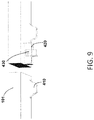
- FIGS. 7 to 9 illustrate perspective views of an exemplary mechanical connection structure for an antenna system incorporating aspects of the disclosed embodiments.
- FIG. 10 illustrates exemplary switching circuits that can be used in an antenna system incorporating aspects of the disclosed embodiments.
- FIGS. 11 to 14 illustrate exemplary electromagnetic field flows for an antenna system incorporating aspects of the disclosed embodiments.
- FIG. 1A there can be seen an exemplary schematic block diagram of an antenna system 100 for a mobile communication device 10 incorporating aspects of the disclosed embodiments.
- the aspects of the disclosed embodiments provide an antenna system for a mobile device that has separate and independent multiple-input multiple-output (MIMO) antennas.
- MIMO multiple-input multiple-output
- the mobile device 10 includes a metal chassis portion 104 with a metal frame member 101 .
- the metal frame member 101 also referred to herein as a first electrically conducting member 101 , generally comprises the electrically conducting members of the antenna system 100 incorporating aspects of the disclosed embodiments.
- the metal frame member 101 is made up of a plurality of segment-type metal frame parts or members. In one embodiment, the metal frame 101 can be used to provide structural support for the mobile device 10 .
- the plurality of segments of the metal frame 101 include at least a first corner segment 110 and a central segment 120 .
- the central segment 120 is generally disposed substantially adjacent to the first corner segment 110 .
- the central segment 120 and the first corner segment 110 can form separate and independent MIMO antennas for the antenna system 100 .
- the first corner segment 110 of the metal frame member 101 comprises an antenna radiating element that can be configured to operate at cellular mid-high frequency bands. These corner segment antenna radiating elements are also referred to herein as corner antennas.
- the first corner segment 110 of the metal frame 101 can be configured to form a low band antenna that is configured to radiate on multiple cellular frequency bands.
- the central segment 120 can be configured to form a mid-to-high band antenna, also referred to as the center mid-high band antenna.
- a gap 174 is maintained between the first corner segment 110 and the central segment 120 .
- a dielectric material 171 can be disposed in the gap 174 .
- the dielectric material 171 can comprise any suitable dielectric material, such as for example, air.
- the gaps, such as gap 174 in the metal frame 101 generally improve the in-hand performance of the center mid-high band antenna.
- the antenna system 100 includes a second electrically conductive structure or member 102 , also referred to herein as an “internal conductive member.”
- the second electrically conductive member 102 is configured to run along or adjacent to at least a portion of the exterior metal frame structure 101 , such as the center part of the metal frame structure 101 .
- the second electrically conductive member 102 can be formed as at least one conductive track on a dielectric part of the mobile device 10 .
- the second electrically conductive member 102 can be formed on a printed circuit board 103 of the mobile device 10 .
- the second electrically conductive member 102 will be disposed under the front glass cover or screen of the mobile device 10 , above the bottom connector portions, for example.
- the second electrically conductive member 102 is connected to the first corner segment 110 .
- the second electrically conductive member 102 can be connected to any suitable parts of the metal frame 101 , such as another corner segment of the metal frame structure 101 , as will be described herein.
- a first end 107 of the second electrically conductive member 102 is connected to the first corner segment 110 .
- a portion 112 of the second electrically conductive member 102 away from the first end 107 is electrically connected to a first feed portion or circuit in, also referred to herein as an RF feeding point.
- the portion 112 can be considered the end of the second electrically conductive member 102 opposing the first end 107 .
- the RF feeding point 111 allows the internal conductive structure to be configured as a “low-band” antenna.
- At least one second feed portion or circuit 121 is connected to the central segment 120 of the metal frame structure 101 , also referred to herein as the center part 120 .
- the central segment 120 can be configured as the “center” antenna.
- the first feed portion or circuit in and the second feed portion or circuit 121 generally comprise RF circuits or feeds configured for different frequency bands and/or separate and independent MIMO antennas.
- the first feed portion in and the second feed portion 121 can comprise the same circuit on a single printed circuit board, such as circuit board 103 , or be different circuits on the same or different printed circuit boards of the mobile device 10 .
- a length of the second electrically conductive member 102 can be configured to be approximately equal to a quarter wavelength @ minimum frequency. For example 700 MHz ⁇ 58 mm; 1700 MHz ⁇ 24 mm.
- the second electrically conductive member 102 should generally be located close to edges of the mobile device 10 in order to radiate efficiently and should be positioned in a proximity to the central segment 120 .
- At least a portion or segment 114 of the second electrically conductive member 102 is configured to be disposed in proximity to the central segment 120 .
- the central segment 120 is disposed along a bottom portion of the mobile device 10 .
- the segment 114 runs along and is disposed in a substantially parallel relationship relative to the central segment 120 .
- the second electrically conductive member 102 is configured as a low-impedance feeding of the first corner segment 110 .
- the length of the second conductive member 102 and the proximity of the second conductive member 102 to the edges of the mobile device 10 generally dictate the necessity of having a segment 114 that is disposed in a substantially parallel relationship relative to the central segment 120 .
- the antenna system 100 can be configured to allocate three independent antennas at or near a bottom side 12 of the mobile device 10 .
- the “bottom side” or portion of the mobile device 10 generally refers to a side that is not in contact with the hand of the user while the phone is being used. As is generally understood, the tendency is to hold a phone along two sides, such as sides 14 and 16 in FIG. 1B , while using the mobile device 10 , such as when holding the mobile device 10 to the ear. A side of the mobile device 10 that is not in contact with the user's hand in this usage position can be considered the bottom portion or side 12 of the mobile device 10 .
- the bottom portion or side 12 of the mobile device 10 includes three separate and independent antenna segments, generally comprising the first corner segment 110 , the central segment 120 and another or second corner segment 130 .
- the first corner segment 110 and the second corner segment 130 are generally formed as elongation of the metal frame 101 towards the corner areas of the mobile device 10 .
- one side 108 of the corner segment 110 is in proximity to the central segment 120 , while the other side 116 is conductively connected to the metal chassis 104 .
- the three separate and independent antenna segments, 110 , 120 and 130 provide a better environment to match them independently and separately, such as for example, a low-band (LB) and two mid-high band (MHB) antennas. This enables optimal low-pass, high pass filter type matching circuits.
- LB low-band
- MHB mid-high band
- the corner, or low band antenna in FIG. 1B is formed by the second electrically conductive member 102 connected to at least one corner part 110 of the metal frame 101 .
- This corner low band antenna 110 in the example of FIG. 1 can be configured to radiate at multiple cellular frequency bands.
- the central segment 120 is connected to the second feed portion 121 , while the second corner segment 130 is connected to the third feed portion or RF circuit 131 that is disposed on or part of the printed circuit board 103 .
- a dielectric such as the dielectric 171 , fills the gap 176 between the central segment 120 and the second corner segment 130 .
- the end portion or segment 116 of first corner segment 110 and the end portion or segment 136 of the second corner segment 130 are isolated from the metal chassis 104 of the mobile device 10 by gaps 172 and 178 .
- the gaps 172 and 178 can be filled with a dielectric material, such as the dielectric material 171 .
- the metal frame 101 is disposed around a perimeter of the mobile device 10 .
- the first corner segment 110 and the second corner segment 130 are isolated from the metal chassis 104 by the dielectric filled gaps 172 , 178 .
- four physical gaps are created in the metal frame 101 .
- This configuration can also allow the mid-high band antenna in the central segment 120 to be generally immune to left and right hand gripping of the mobile device 10 , which provides more balanced right and left hand performance.
- the segments 181 and 182 of the metal frame 101 are connected to ground.
- FIG. 2A illustrates another exemplary embodiment of antenna system 100 for a mobile device 10 incorporating aspects of the disclosed embodiments.
- the corner antenna 110 is connected to the second electrically conductive member 102 , which is connected to the first feed or RF circuits 111 .
- the first feed 111 can also be referred to as a low band feeding connection.
- the low band antenna is formed by the second electrically conductive member 102 connected to the first corner segment 110 .
- the second electrically conductive member 102 and the first corner or low band antenna 110 are connected to RF circuits on the PCB 103 with the first feed or low band feeding connection 111 and a low band tunable impedance loading connection 142 .
- the central segment 120 is connected to the RF circuits on the PCB 103 with the second feed 121 and a tunable impedance loading connection 122 .
- the second corner segment 130 is connected to the RF circuits on the PCB with the third feed 131 and a tunable impedance loading connection 132 .
- the second corner antenna 130 is configured as a MIMO antenna operating at cellular mid-high frequency bands, such as for example, 1470 MHz-2700 MHz.
- the corner feed 131 is allocated to provide impedance matching for the structure and efficient antenna radiation.
- the second corner antenna 130 is formed as inverted-F antenna by the grounding point 150 connection to the PCB 103 .
- the second corner antenna 130 can further include a tunable impedance loading 132 connection to the PCB 103 .
- the central segment or center antenna 120 is configured as another MIMO antenna operating in cellular mid-high frequency bands, for example 1470 MHz-2700 MHz.
- the center antenna 120 comprises a center part of the metal frame 101 , which in this example is along the bottom portion 12 of the mobile device.
- a center feed 121 connects the center antenna 120 to RF circuits on the PCB 103 , providing impedance matching for the structure and efficient antenna radiation.
- the center antenna 120 can further include at least one ground and impedance loading circuit or connection 122 to the PCB 103 , providing a plurality of resonant frequencies within cellular mid-high frequency bands.
- the center antenna 120 of the metal frame 101 in FIG. 2B is electrically isolated from the corner segments 110 , 130 by the dielectrics-filled gaps 174 and 176 and generally orthogonal current modes. In this manner, the center antenna 120 is substantially isolated from the corner antenna 130 by at least 10 dB within operating cellular mid-high frequency bands.
- isolation between the low-band or corner antenna 110 and the center antenna 120 is provided by the impedance matching circuit or circuits 142 and the impedance matching circuit or circuits 122 .
- the impedance matching circuits 142 of the low-band feed 111 can be generally configured as a low-pass filter, and the impedance matching circuit or circuits 122 of the center feed 121 as a high-pass filter.
- the allocation of the center antenna 120 provides maximum clearance from the adjacent metal parts of the mobile device 10 .
- Open boundary conditions are defined in proximity to the sides and center of the mobile device 10 , such as sides 14 and 16 . This enables radiating a maximum E-field at the sides and center of the mobile device 10 and minimizing energy dissipation within user's hand and head.
- the corner antennas 110 and 130 include feeding connections 111 , 131 , respectively, to corresponding circuits on the PCB 103 .
- the first corner antenna 110 can include at least one ground connection 151 and impedance loading connections 142 to corresponding circuits disposed for example on the PCB 103 , providing plurality of resonant frequencies within cellular mid-high frequency bands.
- the ground connection 151 for the first corner antenna 110 can be provided by internal conductive structures, further increasing antenna length and thus improving radiation efficiency.
- the first corner antenna 110 , center antenna 120 and second corner antenna 130 can also have different antenna configurations, such as for example, monopole or ILA (inverted-L antenna), loop etc.
- FIG. 3 illustrates a front view of the bottom 12 and side portions 14 , 16 of a mobile device 10 with an antenna system 100 including aspects of the disclosed embodiments.
- the second electrically conductive member 102 is formed by at least one conductor track disposed on or connected to a dielectric part of the mobile device 10 , such as the PCB 103 .
- the second electrically conductive element 102 enables spatial reuse.
- the first corner or low-band antenna 110 and the center antenna 120 and second corner antenna 130 , or two mid-high band antennas utilize the same volume within the bottom portion 12 of the mobile device 10 .
- Each antenna element 110 , 120 and 130 is configured to radiate in at least one MIMO frequency band. In this manner, spatial reuse provides for the allocation of multiple antennas within what would otherwise be the same volume for a single antenna.
- the second electrically conductive member 102 can be disposed under a front glass cover, generally illustrated by 302 , of the mobile device 10 , which is also disposed above a Universal Serial Bus (USB) connector 210 and an audio-visual (AV) jack 220 , as may be generally understood.
- USB Universal Serial Bus
- AV audio-visual
- the second electrically conductive member 102 is connected to the corner antenna 110 and the low-band antenna 130 via contact points or connections 231 , 232 .
- Low-band feed in and low-band tunable impedance loading 142 are conductively connected to the second electrically conductive structure 102 .
- the embodiment of FIG. 3 provides three independent antenna elements: the first corner or low band antenna 110 and two mid-high band antennas, the center antenna 120 and the second corner antenna 130 .
- the two mid-high band antennas 120 , 130 can be configured for 4 ⁇ 4 MIMO multiband operation.
- Each of the three independent antennas 110 , 120 , 130 can have a separate feeding connection, such as 111 , 121 , 131 shown in FIG. 2B , and independently configured multiband impedance matching 142 , 122 and 132 .
- FIGS. 4 and 5 illustrates one embodiment of the connections of the second electrically conductive member or structure 102 to the PCB 103 and the corresponding circuits.
- the examples of FIGS. 4 and 5 illustrate a perspective view of the front and back of the bottom portion 12 of a mobile device 10 that includes an antenna structure 100 incorporating aspects of the disclosed embodiments.
- connection points 231 and 232 generally illustrate an exemplary connection of the second electrically conductive member 102 to the first corner antenna 110 and the second corner antenna 130 , respectively.
- Connection points 233 , 234 and 235 illustrate exemplary connections for the feeding point 111 , impedance circuits 142 and ground 150 illustrated in FIG. 2B , for example, to the second electrically conductive member 102 . While certain connection points are illustrated in the example of FIGS. 4 and 5 , also with respect to FIG. 2B , the aspects of the disclosed embodiments are not so limited. In alternate embodiments, the manner of connection and the order of connections can be any suitable or desired connection type.
- FIG. 6 illustrates one example of the second electrically conductive structure 102 .
- the second electrically conductive structure 102 is affixed to a plastic carrier 310 and metal parts 320 of the mobile device 10 .
- Exemplary manufacturing methods for producing the second electrically conductive structure 102 can include, but are not limited to, fabrication of the conductive structure 102 as a separate Laser Direct Structuring (LDS) part; printing the conductive structure 102 using 3D printing technology, affixing a flexible PCB on a plastic carrier, stamping a metal part, inserting a moulded metal part, or as part of a metal ring itself.
- LDS Laser Direct Structuring
- Connection points or contacts 330 are allocated for connection of the second electrically conductive structure 102 to the PCB 103 or metal frame parts, generally as shown with respect to FIGS. 4 and 5 , for example.
- the connection points or contacts 330 generally comprise one or more of the connections points 231 - 235 illustrated in FIGS. 4 and 5 .
- connection points or contacts 330 can comprise c-clip type members or contact points as a mechanical interface for the connection points 231 - 235 illustrated in FIGS. 4 and 5 .
- connection points 330 generally comprise bus-stop members 410 , 420 and c-clip type contacts 430 .
- the bus stop members 410 , 420 are shown in FIGS. 7 and 8 as being connected to the first electrically conductive member 101 and the second electrically conductive member 102 via c-clip members 430 .
- the c-clip members 430 are shown in this example as being connected to the first electrically conductive member 101 . Engagement of the bus stop or contact member 420 with a c-clip member 430 can be used to electrically connect the first electrically conducting member 101 , or segments of the metal frame 104 , to the second electrically conductive member 102 as is generally described herein.
- the aspects of the disclosed embodiments provides a MIMO antenna arrangement, for example, main low-band antenna, main mid-high band antenna, multiband MIMO antenna or any combination thereof, or a complete MIMO antenna arrangement on its own.
- this is enabled by configuring the operational frequency bands of the center antennas and the corner antennas to be at least partially overlapping.
- This configuration advantageously enables the antenna arrangement 100 of the disclosed embodiments to provide a MIMO antenna or a diversity antenna.
- the operational frequency bands of center antennas and corner antennas may be Long Term Evolution (LTE) frequency bands.
- Exemplary tuneable impedance matching circuits 501 , 502 for embodiments of the antenna system 100 are illustrated in FIG. 10 .
- the tuneable impedance matching circuits 501 , 502 are generally utilized for providing multi-band operation of the MIMO antennas. For example, covering all low-frequency bands from B12 to B8.
- the exemplary circuits 501 , 502 generally include a fixed matching circuit 530 and switching matching circuits 540 .
- Exemplary embodiments of the switching matching circuits 532 can include an SPnT switch with different inductors L1, L2, L3 to the ground, including SPST, SPDT, SP4T, for example.
- the exemplary embodiments may include any type of switch realized in any suitable technology, such as for example as semiconductor (SOI, CMOS, GaAs, GaN etc), MEMS technology.
- Other embodiments of tuneable impedance matching circuits 501 , 502 may utilize capacitance banks, varactors or other reconfigurable impedance circuits.
- the antenna feed connection 510 could be spatially separated from antenna tuneable impedance connection 520 as illustrated by circuit 502 .
- circuit 502 separate contact points 231 , 232 can be used, as illustrated with respect to FIGS. 4 and 5 .
- the antenna feed connection 510 could be co-allocated with antenna tuneable impedance connection 520 .
- a length of the second electrically conductive member 102 disclosed herein is independent of a geometry of the mobile device 10 . Therefore, a length of the low-band antenna, such as the first corner antenna 110 described herein, can be adjusted to meet appropriate resonance conditions. For example, at a resonance frequency of 800 MHz, an efficiency of the low-band antenna 110 can be maximized within entire frequency band 698 MHz-960 MHz. Illustrations of low-band antenna frequency responses for various states of the switch 501 , 502 shown in FIG. 10 , are illustrated in FIGS. 11-14 . Prototype measurement results included: ⁇ 6.1 dB eff 80 MHz BW measured in B8; ⁇ 5.8 dB 50 MHz BW measured at B12.
- FIG. 11 illustrates operation of the first corner or low band antenna 110 at low-bands frequency range 699-960 MHz: surface currents distribution 1110 and E-field lines of force distribution 1120 .
- the antenna 110 operates as a monopole or an IFA at low-bands frequency range.
- FIG. 12 illustrates an exemplary operation of the center segment or antenna 120 at high-bands frequency range (1900-2700 MHz).
- the surface currents distribution 1210 and E-field lines of force distribution 1220 are illustrated.
- the antenna 120 operates as a slot or a loop type antenna at high-bands frequency range.
- FIG. 13 illustrates an exemplary operation of the center segment or antenna 120 at low-bands frequency range (699-960 MHz), or at mid-bands frequency range (1450-1900 MHz).
- the surface currents distribution 1310 and E-field lines of force distribution 1320 are illustrated.
- the center antenna 120 operates as a monopole or a IFA at low-bands frequency range.
- FIG. 14 illustrates operation of the second corner antenna 130 at mid-high bands frequency range (1700-2700 MHz).
- the surface currents distribution 1410 and E-field lines of force distribution 1420 are illustrated.
- the second corner antenna 130 operates as a monopole or an IFA at mid-high bands frequency range.
- FIGS. 11-14 illustrates radiation modes of the antennas 110 , 120 , 130 at cellular frequency bands, their orthogonally and mutual isolation.
- Surface currents distributions 1410 of the first corner antenna 110 are not overlapping in space with surface currents distributions 1110 of the second corner antenna 130 . Thus high isolation between the corner antennas 110 and 130 is achieved.
- the surface currents distributions mo of first corner antenna 110 are partially overlapping in space with surface currents distributions 1210 , 1310 of the center antenna 120 .
- isolation between antennas 120 and no is achieved by separating their feeding connections 121 , 111 respectively and operating antennas 120 and no at non-overlapping frequency bands.
- the first corner antenna 110 can be operated at low frequency bands, while the center antenna 120 is operating at mid-high frequency bands.
- antenna 130 is operating at mid-high frequency bands, antenna 120 is operating at low frequency bands.
- the aspects of the disclosed embodiments provide an antenna system for a mobile device that has separate and independent multiple-input multiple-output (MIMO) antennas.
- MIMO multiple-input multiple-output
- the antenna system of the disclosed embodiments makes use of the exterior metal frame, metal back cover and internal conductive member to provide separate and independent antenna systems.
- the separate and independent antennas enable multiband 4 ⁇ 4 MIMO operation of the cellular communication networks.
Landscapes
- Engineering & Computer Science (AREA)
- Computer Networks & Wireless Communication (AREA)
- Support Of Aerials (AREA)
- Details Of Aerials (AREA)
Abstract
Description
Claims (20)
Applications Claiming Priority (1)
| Application Number | Priority Date | Filing Date | Title |
|---|---|---|---|
| PCT/EP2017/075385 WO2019068331A1 (en) | 2017-10-05 | 2017-10-05 | Antenna system for a wireless communication device |
Publications (2)
| Publication Number | Publication Date |
|---|---|
| US20200321688A1 US20200321688A1 (en) | 2020-10-08 |
| US11223106B2 true US11223106B2 (en) | 2022-01-11 |
Family
ID=60138352
Family Applications (1)
| Application Number | Title | Priority Date | Filing Date |
|---|---|---|---|
| US16/753,513 Active 2037-11-02 US11223106B2 (en) | 2017-10-05 | 2017-10-05 | Antenna system for a wireless communication device |
Country Status (4)
| Country | Link |
|---|---|
| US (1) | US11223106B2 (en) |
| EP (1) | EP3682507B1 (en) |
| CN (1) | CN111492535B (en) |
| WO (1) | WO2019068331A1 (en) |
Cited By (6)
| Publication number | Priority date | Publication date | Assignee | Title |
|---|---|---|---|---|
| US20210151886A1 (en) * | 2018-05-15 | 2021-05-20 | Huawei Technologies Co., Ltd. | Antenna System and Terminal Device |
| US20210399420A1 (en) * | 2020-06-23 | 2021-12-23 | Beijing Xiaomi Mobile Software Co., Ltd. | Antenna module and terminal device |
| US20220069468A1 (en) * | 2020-08-28 | 2022-03-03 | Chiun Mai Communication Systems, Inc. | Antenna structure and wireless communication device using same |
| US20230275345A1 (en) * | 2020-06-04 | 2023-08-31 | Huawei Technologies Co., Ltd. | Electronic Device |
| US20240113415A1 (en) * | 2022-10-04 | 2024-04-04 | Samsung Electronics Co., Ltd. | Electronic device including conductive portions of housing operating as antenna |
| US20250125520A1 (en) * | 2023-10-13 | 2025-04-17 | Quanta Computer Inc. | Wearable device |
Families Citing this family (11)
| Publication number | Priority date | Publication date | Assignee | Title |
|---|---|---|---|---|
| WO2019117332A1 (en) | 2017-12-12 | 2019-06-20 | 엘지전자 주식회사 | Antenna apparatus and mobile terminal having same |
| CN110784564B (en) * | 2018-07-31 | 2021-09-14 | 华为技术有限公司 | Mobile terminal and preparation method of antenna thereof |
| CN110838612B (en) * | 2018-08-17 | 2021-12-28 | 深圳富泰宏精密工业有限公司 | Antenna structure and wireless communication device with same |
| CN110970709B (en) * | 2018-09-28 | 2022-02-11 | 深圳富泰宏精密工业有限公司 | Antenna structure and wireless communication device with same |
| CN110289485A (en) * | 2019-06-27 | 2019-09-27 | 合肥联宝信息技术有限公司 | A kind of antenna and electronic equipment |
| WO2020258178A1 (en) * | 2019-06-27 | 2020-12-30 | 瑞声声学科技(深圳)有限公司 | Antenna assembly and electronic device |
| WO2021000170A1 (en) * | 2019-06-30 | 2021-01-07 | 瑞声声学科技(深圳)有限公司 | Full-screen electronic device and antenna thereof |
| CN115395208A (en) * | 2019-08-22 | 2022-11-25 | 华为技术有限公司 | Antenna assembly and electronic equipment with curled screen |
| CN113078444B (en) * | 2020-01-06 | 2024-06-11 | 深圳富泰宏精密工业有限公司 | Antenna structure and wireless communication device with same |
| CN113161721B (en) * | 2020-01-22 | 2023-11-28 | 华为技术有限公司 | Antenna devices and electronic equipment |
| CN115332792B (en) * | 2021-05-11 | 2025-05-13 | Oppo广东移动通信有限公司 | Antenna structure and electronic equipment |
Citations (33)
| Publication number | Priority date | Publication date | Assignee | Title |
|---|---|---|---|---|
| US8493272B2 (en) | 2007-06-22 | 2013-07-23 | Nokia Corporation | Apparatus, method and computer program for wireless communication |
| US8907853B2 (en) * | 2012-07-26 | 2014-12-09 | Sony Corporation | Wireless electronic devices with multiple curved antennas along an end portion, and related antenna systems |
| WO2015007952A1 (en) | 2013-07-19 | 2015-01-22 | Nokia Corporation | Apparatus and methods for wireless communication |
| US20150333390A1 (en) | 2014-05-16 | 2015-11-19 | Wistron Neweb Corporation | Wideband Antenna and Wireless Communication Device |
| WO2016000155A1 (en) | 2014-06-30 | 2016-01-07 | 华为技术有限公司 | Seamless sealed-frame antenna and wireless communications device |
| US9236659B2 (en) * | 2013-12-04 | 2016-01-12 | Apple Inc. | Electronic device with hybrid inverted-F slot antenna |
| WO2016005659A1 (en) | 2014-07-10 | 2016-01-14 | Nokia Technologies Oy | Apparatus and methods for wireless communication |
| US20160049719A1 (en) | 2014-08-15 | 2016-02-18 | Wistron Neweb Corporation | Wireless Communication Device |
| US20160064820A1 (en) | 2014-09-02 | 2016-03-03 | Samsung Electronics Co., Ltd. | Antenna using exterior metal frame and electronic device utilizing the same |
| US20160112551A1 (en) | 2015-01-06 | 2016-04-21 | Mediatek Inc. | Metal-Frame Slot Antenna With Matching Circuit And Apparatus Thereof |
| WO2016064415A1 (en) | 2014-10-24 | 2016-04-28 | Hewlett-Packard Development Company, L.P. | Mobile computing device antenna |
| WO2016065630A1 (en) | 2014-10-31 | 2016-05-06 | 华为技术有限公司 | Wireless mobile device |
| US9350069B2 (en) * | 2012-01-04 | 2016-05-24 | Apple Inc. | Antenna with switchable inductor low-band tuning |
| US20160226144A1 (en) | 2015-02-02 | 2016-08-04 | Galtronics Corporation Ltd. | Multi-input multi-output antenna |
| US9413058B1 (en) | 2015-07-10 | 2016-08-09 | Amazon Technologies, Inc. | Loop-feeding wireless area network (WAN) antenna for metal back cover |
| EP3057176A1 (en) | 2015-02-11 | 2016-08-17 | Xiaomi Inc. | Antenna module and mobile terminal |
| US9431693B2 (en) * | 2011-02-25 | 2016-08-30 | Lg Electronics Inc. | Mobile terminal |
| US9521222B1 (en) * | 2015-11-25 | 2016-12-13 | Acer Incorporated | Mobile communication device |
| US20170033812A1 (en) | 2015-07-28 | 2017-02-02 | Samsung Electronics Co., Ltd | Antenna device and electronic device including same |
| US20170048363A1 (en) | 2015-08-13 | 2017-02-16 | Samsung Electronics Co., Ltd. | Antenna and electronic device including the same |
| US20170047639A1 (en) | 2015-08-10 | 2017-02-16 | Samsung Electronics Co., Ltd. | Antenna device and electronic device including the same |
| US9577315B2 (en) * | 2010-08-27 | 2017-02-21 | Apple Inc. | Antennas mounted under dielectric plates |
| US9596330B2 (en) * | 2010-11-05 | 2017-03-14 | Apple Inc. | Antenna system with receiver diversity and tunable matching circuit |
| US9673507B2 (en) * | 2011-02-11 | 2017-06-06 | Pulse Finland Oy | Chassis-excited antenna apparatus and methods |
| WO2017092003A1 (en) | 2015-12-03 | 2017-06-08 | 华为技术有限公司 | Metal frame antenna and terminal device |
| US20170201010A1 (en) | 2016-01-11 | 2017-07-13 | Lg Electronics Inc. | Mobile terminal |
| US9819071B2 (en) * | 2012-08-20 | 2017-11-14 | Nokia Technologies Oy | Antenna apparatus and method of making same |
| US9871286B2 (en) * | 2012-09-19 | 2018-01-16 | Lg Electronics Inc. | Mobile terminal |
| US9876274B2 (en) * | 2014-03-04 | 2018-01-23 | Jae Beom Kim | Antenna radiator having heterogeneous antennas cross-linked with each other and manufacturing method therefor |
| US9876272B2 (en) * | 2015-08-18 | 2018-01-23 | Apple Inc. | Electronic device antenna with embedded parasitic arm |
| US10283844B2 (en) * | 2016-09-23 | 2019-05-07 | Apple Inc. | Electronic devices having housing-integrated distributed loop antennas |
| US10290946B2 (en) * | 2016-09-23 | 2019-05-14 | Apple Inc. | Hybrid electronic device antennas having parasitic resonating elements |
| EP3576221A1 (en) | 2017-01-26 | 2019-12-04 | LG Electronics Inc. -1- | Mobile terminal |
-
2017
- 2017-10-05 EP EP17786863.5A patent/EP3682507B1/en active Active
- 2017-10-05 CN CN201780095453.9A patent/CN111492535B/en active Active
- 2017-10-05 WO PCT/EP2017/075385 patent/WO2019068331A1/en not_active Ceased
- 2017-10-05 US US16/753,513 patent/US11223106B2/en active Active
Patent Citations (47)
| Publication number | Priority date | Publication date | Assignee | Title |
|---|---|---|---|---|
| US8493272B2 (en) | 2007-06-22 | 2013-07-23 | Nokia Corporation | Apparatus, method and computer program for wireless communication |
| US9577315B2 (en) * | 2010-08-27 | 2017-02-21 | Apple Inc. | Antennas mounted under dielectric plates |
| US9596330B2 (en) * | 2010-11-05 | 2017-03-14 | Apple Inc. | Antenna system with receiver diversity and tunable matching circuit |
| US9673507B2 (en) * | 2011-02-11 | 2017-06-06 | Pulse Finland Oy | Chassis-excited antenna apparatus and methods |
| US9431693B2 (en) * | 2011-02-25 | 2016-08-30 | Lg Electronics Inc. | Mobile terminal |
| US9350069B2 (en) * | 2012-01-04 | 2016-05-24 | Apple Inc. | Antenna with switchable inductor low-band tuning |
| US8907853B2 (en) * | 2012-07-26 | 2014-12-09 | Sony Corporation | Wireless electronic devices with multiple curved antennas along an end portion, and related antenna systems |
| US9819071B2 (en) * | 2012-08-20 | 2017-11-14 | Nokia Technologies Oy | Antenna apparatus and method of making same |
| US9985337B2 (en) * | 2012-09-19 | 2018-05-29 | Lg Electronics Inc. | Mobile terminal |
| US9871286B2 (en) * | 2012-09-19 | 2018-01-16 | Lg Electronics Inc. | Mobile terminal |
| US20160164169A1 (en) | 2013-07-19 | 2016-06-09 | Nokia Technologies Oy | Apparatus and methods for wireless communication |
| WO2015007952A1 (en) | 2013-07-19 | 2015-01-22 | Nokia Corporation | Apparatus and methods for wireless communication |
| US9236659B2 (en) * | 2013-12-04 | 2016-01-12 | Apple Inc. | Electronic device with hybrid inverted-F slot antenna |
| US9876274B2 (en) * | 2014-03-04 | 2018-01-23 | Jae Beom Kim | Antenna radiator having heterogeneous antennas cross-linked with each other and manufacturing method therefor |
| US20150333390A1 (en) | 2014-05-16 | 2015-11-19 | Wistron Neweb Corporation | Wideband Antenna and Wireless Communication Device |
| WO2016000155A1 (en) | 2014-06-30 | 2016-01-07 | 华为技术有限公司 | Seamless sealed-frame antenna and wireless communications device |
| US10079427B2 (en) | 2014-06-30 | 2018-09-18 | Huawei Technologies Co., Ltd. | Antenna with slitless closed frame and wireless communications device |
| US10707579B2 (en) | 2014-07-10 | 2020-07-07 | Nokia Technologies Oy | Apparatus and methods for wireless communication |
| WO2016005659A1 (en) | 2014-07-10 | 2016-01-14 | Nokia Technologies Oy | Apparatus and methods for wireless communication |
| US20160049719A1 (en) | 2014-08-15 | 2016-02-18 | Wistron Neweb Corporation | Wireless Communication Device |
| US20160064820A1 (en) | 2014-09-02 | 2016-03-03 | Samsung Electronics Co., Ltd. | Antenna using exterior metal frame and electronic device utilizing the same |
| US10224610B2 (en) | 2014-10-24 | 2019-03-05 | Hewlett-Packard Development Company, L.P. | Mobile computing device antenna |
| WO2016064415A1 (en) | 2014-10-24 | 2016-04-28 | Hewlett-Packard Development Company, L.P. | Mobile computing device antenna |
| US10347988B2 (en) | 2014-10-31 | 2019-07-09 | Huawei Technologies Co., Ltd. | Wireless mobile device |
| WO2016065630A1 (en) | 2014-10-31 | 2016-05-06 | 华为技术有限公司 | Wireless mobile device |
| US20160112551A1 (en) | 2015-01-06 | 2016-04-21 | Mediatek Inc. | Metal-Frame Slot Antenna With Matching Circuit And Apparatus Thereof |
| US10522909B2 (en) * | 2015-02-02 | 2019-12-31 | Galtronics Usa, Inc. | Multi-input multi-output antenna |
| US20160226144A1 (en) | 2015-02-02 | 2016-08-04 | Galtronics Corporation Ltd. | Multi-input multi-output antenna |
| EP3057176A1 (en) | 2015-02-11 | 2016-08-17 | Xiaomi Inc. | Antenna module and mobile terminal |
| US10186755B2 (en) | 2015-02-11 | 2019-01-22 | Xiaomi Inc. | Antenna module and mobile terminal using the same |
| US9413058B1 (en) | 2015-07-10 | 2016-08-09 | Amazon Technologies, Inc. | Loop-feeding wireless area network (WAN) antenna for metal back cover |
| US10594344B2 (en) * | 2015-07-28 | 2020-03-17 | Samsung Electronics Co., Ltd. | Antenna device and electronic device including same |
| US10218396B2 (en) * | 2015-07-28 | 2019-02-26 | Samsung Electronics Co., Ltd. | Antenna device and electronic device including same |
| US20170033812A1 (en) | 2015-07-28 | 2017-02-02 | Samsung Electronics Co., Ltd | Antenna device and electronic device including same |
| US20170047639A1 (en) | 2015-08-10 | 2017-02-16 | Samsung Electronics Co., Ltd. | Antenna device and electronic device including the same |
| US10224608B2 (en) * | 2015-08-10 | 2019-03-05 | Samsung Electronics Co., Ltd. | Antenna device and electronic device including the same |
| US9762710B2 (en) * | 2015-08-13 | 2017-09-12 | Samsung Electronics Co., Ltd. | Antenna and electronic device including the same |
| US20170048363A1 (en) | 2015-08-13 | 2017-02-16 | Samsung Electronics Co., Ltd. | Antenna and electronic device including the same |
| US9876272B2 (en) * | 2015-08-18 | 2018-01-23 | Apple Inc. | Electronic device antenna with embedded parasitic arm |
| US9521222B1 (en) * | 2015-11-25 | 2016-12-13 | Acer Incorporated | Mobile communication device |
| WO2017092003A1 (en) | 2015-12-03 | 2017-06-08 | 华为技术有限公司 | Metal frame antenna and terminal device |
| US10256527B2 (en) * | 2016-01-11 | 2019-04-09 | Lg Electronics Inc. | Mobile terminal |
| CN107026326A (en) | 2016-01-11 | 2017-08-08 | Lg电子株式会社 | Mobile terminal |
| US20170201010A1 (en) | 2016-01-11 | 2017-07-13 | Lg Electronics Inc. | Mobile terminal |
| US10283844B2 (en) * | 2016-09-23 | 2019-05-07 | Apple Inc. | Electronic devices having housing-integrated distributed loop antennas |
| US10290946B2 (en) * | 2016-09-23 | 2019-05-14 | Apple Inc. | Hybrid electronic device antennas having parasitic resonating elements |
| EP3576221A1 (en) | 2017-01-26 | 2019-12-04 | LG Electronics Inc. -1- | Mobile terminal |
Cited By (10)
| Publication number | Priority date | Publication date | Assignee | Title |
|---|---|---|---|---|
| US20210151886A1 (en) * | 2018-05-15 | 2021-05-20 | Huawei Technologies Co., Ltd. | Antenna System and Terminal Device |
| US11735809B2 (en) * | 2018-05-15 | 2023-08-22 | Huawei Technologies Co., Ltd. | Antenna system and terminal device |
| US20230275345A1 (en) * | 2020-06-04 | 2023-08-31 | Huawei Technologies Co., Ltd. | Electronic Device |
| US20210399420A1 (en) * | 2020-06-23 | 2021-12-23 | Beijing Xiaomi Mobile Software Co., Ltd. | Antenna module and terminal device |
| US11462829B2 (en) * | 2020-06-23 | 2022-10-04 | Beijing Xiaomi Mobile Software Co., Ltd. | Antenna module and terminal device |
| US20220069468A1 (en) * | 2020-08-28 | 2022-03-03 | Chiun Mai Communication Systems, Inc. | Antenna structure and wireless communication device using same |
| US11923599B2 (en) * | 2020-08-28 | 2024-03-05 | Chiun Mai Communication Systems, Inc. | Antenna structure and wireless communication device using same |
| US20240113415A1 (en) * | 2022-10-04 | 2024-04-04 | Samsung Electronics Co., Ltd. | Electronic device including conductive portions of housing operating as antenna |
| US20250125520A1 (en) * | 2023-10-13 | 2025-04-17 | Quanta Computer Inc. | Wearable device |
| US12418101B2 (en) * | 2023-10-13 | 2025-09-16 | Quanta Computer Inc. | Wearable device |
Also Published As
| Publication number | Publication date |
|---|---|
| CN111492535A (en) | 2020-08-04 |
| US20200321688A1 (en) | 2020-10-08 |
| WO2019068331A1 (en) | 2019-04-11 |
| CN111492535B (en) | 2021-10-01 |
| EP3682507B1 (en) | 2023-10-04 |
| EP3682507A1 (en) | 2020-07-22 |
Similar Documents
| Publication | Publication Date | Title |
|---|---|---|
| US11223106B2 (en) | Antenna system for a wireless communication device | |
| EP3469656B1 (en) | An antenna system for a portable device | |
| US11018433B2 (en) | Triple wideband hybrid LTE slot antenna | |
| US10522909B2 (en) | Multi-input multi-output antenna | |
| US10581148B2 (en) | External antenna for vehicle | |
| US20130002510A1 (en) | Antennas with novel current distribution and radiation patterns, for enhanced antenna islation | |
| KR20110043637A (en) | Compact multiband antenna | |
| US10109926B2 (en) | Antenna radiator, antenna and mobile terminal | |
| KR20100063414A (en) | Multiband antenna apparatus | |
| US20130234897A1 (en) | Mobile terminal apparatus and method for performing wireless communication using an indirect feeding antenna | |
| US20160190676A1 (en) | Antenna and wireless communication apparatus | |
| US10374311B2 (en) | Antenna for a portable communication device | |
| CN111478042B (en) | Antenna and mobile terminal | |
| CN108134194B (en) | A miniaturized WLAN dual-band PIFA antenna | |
| US10784592B2 (en) | Isolated ground for wireless device antenna | |
| JP2018148533A (en) | Multiband antenna and radio communication equipment | |
| KR100830568B1 (en) | Antenna device for cellular communication terminal | |
| KR100922230B1 (en) | Multilayer antenna | |
| JP6865072B2 (en) | Antenna device and electronic device equipped with an antenna device | |
| KR102887422B1 (en) | Antenna module and antenna device having the same | |
| KR102049755B1 (en) | Multi-band antenna using button device and communication terminal | |
| KR100895658B1 (en) | Low Profile Smart Antennas and Related Methods for Wireless Applications | |
| CN108881541B (en) | Mobile terminal | |
| CN106972272B (en) | Antenna system and mobile terminal | |
| TW202420645A (en) | Highly isolated and barely separated antennas integrated with noise free rf-transparent printed circuit board (pcb) for enhanced radiated sensitivity |
Legal Events
| Date | Code | Title | Description |
|---|---|---|---|
| FEPP | Fee payment procedure |
Free format text: ENTITY STATUS SET TO UNDISCOUNTED (ORIGINAL EVENT CODE: BIG.); ENTITY STATUS OF PATENT OWNER: LARGE ENTITY |
|
| AS | Assignment |
Owner name: HUAWEI TECHNOLOGIES CO., LTD., CHINA Free format text: ASSIGNMENT OF ASSIGNORS INTEREST;ASSIGNORS:KHRIPKOV, ALEXANDER;KROGERUS, JOONAS;SOWPATI, ARUN;AND OTHERS;SIGNING DATES FROM 20200720 TO 20200817;REEL/FRAME:053827/0217 |
|
| STPP | Information on status: patent application and granting procedure in general |
Free format text: DOCKETED NEW CASE - READY FOR EXAMINATION |
|
| STPP | Information on status: patent application and granting procedure in general |
Free format text: NON FINAL ACTION MAILED |
|
| STPP | Information on status: patent application and granting procedure in general |
Free format text: RESPONSE TO NON-FINAL OFFICE ACTION ENTERED AND FORWARDED TO EXAMINER |
|
| STPP | Information on status: patent application and granting procedure in general |
Free format text: NOTICE OF ALLOWANCE MAILED -- APPLICATION RECEIVED IN OFFICE OF PUBLICATIONS |
|
| STPP | Information on status: patent application and granting procedure in general |
Free format text: AWAITING TC RESP., ISSUE FEE NOT PAID |
|
| STPP | Information on status: patent application and granting procedure in general |
Free format text: NOTICE OF ALLOWANCE MAILED -- APPLICATION RECEIVED IN OFFICE OF PUBLICATIONS |
|
| STPP | Information on status: patent application and granting procedure in general |
Free format text: AWAITING TC RESP, ISSUE FEE PAYMENT VERIFIED |
|
| STPP | Information on status: patent application and granting procedure in general |
Free format text: PUBLICATIONS -- ISSUE FEE PAYMENT VERIFIED |
|
| STCF | Information on status: patent grant |
Free format text: PATENTED CASE |
|
| MAFP | Maintenance fee payment |
Free format text: PAYMENT OF MAINTENANCE FEE, 4TH YEAR, LARGE ENTITY (ORIGINAL EVENT CODE: M1551); ENTITY STATUS OF PATENT OWNER: LARGE ENTITY Year of fee payment: 4 |