US11222947B2 - Methods of doping fin structures of non-planar transistor devices - Google Patents
Methods of doping fin structures of non-planar transistor devices Download PDFInfo
- Publication number
- US11222947B2 US11222947B2 US15/757,251 US201515757251A US11222947B2 US 11222947 B2 US11222947 B2 US 11222947B2 US 201515757251 A US201515757251 A US 201515757251A US 11222947 B2 US11222947 B2 US 11222947B2
- Authority
- US
- United States
- Prior art keywords
- fin
- concentration
- dopant species
- substrate
- transistor
- Prior art date
- Legal status (The legal status is an assumption and is not a legal conclusion. Google has not performed a legal analysis and makes no representation as to the accuracy of the status listed.)
- Active
Links
Images


Classifications
-
- H01L29/0638—
-
- H—ELECTRICITY
- H10—SEMICONDUCTOR DEVICES; ELECTRIC SOLID-STATE DEVICES NOT OTHERWISE PROVIDED FOR
- H10D—INORGANIC ELECTRIC SEMICONDUCTOR DEVICES
- H10D62/00—Semiconductor bodies, or regions thereof, of devices having potential barriers
- H10D62/10—Shapes, relative sizes or dispositions of the regions of the semiconductor bodies; Shapes of the semiconductor bodies
- H10D62/102—Constructional design considerations for preventing surface leakage or controlling electric field concentration
- H10D62/112—Constructional design considerations for preventing surface leakage or controlling electric field concentration for preventing surface leakage due to surface inversion layers, e.g. by using channel stoppers
-
- H01L21/223—
-
- H01L21/2253—
-
- H01L21/2254—
-
- H01L21/2652—
-
- H01L21/266—
-
- H01L21/31155—
-
- H01L29/0673—
-
- H01L29/66803—
-
- H01L29/785—
-
- H—ELECTRICITY
- H10—SEMICONDUCTOR DEVICES; ELECTRIC SOLID-STATE DEVICES NOT OTHERWISE PROVIDED FOR
- H10D—INORGANIC ELECTRIC SEMICONDUCTOR DEVICES
- H10D30/00—Field-effect transistors [FET]
- H10D30/01—Manufacture or treatment
- H10D30/021—Manufacture or treatment of FETs having insulated gates [IGFET]
- H10D30/024—Manufacture or treatment of FETs having insulated gates [IGFET] of fin field-effect transistors [FinFET]
- H10D30/0241—Manufacture or treatment of FETs having insulated gates [IGFET] of fin field-effect transistors [FinFET] doping of vertical sidewalls, e.g. using tilted or multi-angled implants
-
- H—ELECTRICITY
- H10—SEMICONDUCTOR DEVICES; ELECTRIC SOLID-STATE DEVICES NOT OTHERWISE PROVIDED FOR
- H10D—INORGANIC ELECTRIC SEMICONDUCTOR DEVICES
- H10D30/00—Field-effect transistors [FET]
- H10D30/60—Insulated-gate field-effect transistors [IGFET]
- H10D30/62—Fin field-effect transistors [FinFET]
-
- H—ELECTRICITY
- H10—SEMICONDUCTOR DEVICES; ELECTRIC SOLID-STATE DEVICES NOT OTHERWISE PROVIDED FOR
- H10D—INORGANIC ELECTRIC SEMICONDUCTOR DEVICES
- H10D62/00—Semiconductor bodies, or regions thereof, of devices having potential barriers
- H10D62/10—Shapes, relative sizes or dispositions of the regions of the semiconductor bodies; Shapes of the semiconductor bodies
- H10D62/117—Shapes of semiconductor bodies
- H10D62/118—Nanostructure semiconductor bodies
- H10D62/119—Nanowire, nanosheet or nanotube semiconductor bodies
- H10D62/121—Nanowire, nanosheet or nanotube semiconductor bodies oriented parallel to substrates
-
- H—ELECTRICITY
- H10—SEMICONDUCTOR DEVICES; ELECTRIC SOLID-STATE DEVICES NOT OTHERWISE PROVIDED FOR
- H10P—GENERIC PROCESSES OR APPARATUS FOR THE MANUFACTURE OR TREATMENT OF DEVICES COVERED BY CLASS H10
- H10P30/00—Ion implantation into wafers, substrates or parts of devices
- H10P30/20—Ion implantation into wafers, substrates or parts of devices into semiconductor materials, e.g. for doping
- H10P30/202—Ion implantation into wafers, substrates or parts of devices into semiconductor materials, e.g. for doping characterised by the semiconductor materials
- H10P30/204—Ion implantation into wafers, substrates or parts of devices into semiconductor materials, e.g. for doping characterised by the semiconductor materials into Group IV semiconductors
-
- H—ELECTRICITY
- H10—SEMICONDUCTOR DEVICES; ELECTRIC SOLID-STATE DEVICES NOT OTHERWISE PROVIDED FOR
- H10P—GENERIC PROCESSES OR APPARATUS FOR THE MANUFACTURE OR TREATMENT OF DEVICES COVERED BY CLASS H10
- H10P30/00—Ion implantation into wafers, substrates or parts of devices
- H10P30/20—Ion implantation into wafers, substrates or parts of devices into semiconductor materials, e.g. for doping
- H10P30/21—Ion implantation into wafers, substrates or parts of devices into semiconductor materials, e.g. for doping of electrically active species
- H10P30/212—Through-implantation
-
- H—ELECTRICITY
- H10—SEMICONDUCTOR DEVICES; ELECTRIC SOLID-STATE DEVICES NOT OTHERWISE PROVIDED FOR
- H10P—GENERIC PROCESSES OR APPARATUS FOR THE MANUFACTURE OR TREATMENT OF DEVICES COVERED BY CLASS H10
- H10P30/00—Ion implantation into wafers, substrates or parts of devices
- H10P30/20—Ion implantation into wafers, substrates or parts of devices into semiconductor materials, e.g. for doping
- H10P30/214—Recoil-implantation
-
- H—ELECTRICITY
- H10—SEMICONDUCTOR DEVICES; ELECTRIC SOLID-STATE DEVICES NOT OTHERWISE PROVIDED FOR
- H10P—GENERIC PROCESSES OR APPARATUS FOR THE MANUFACTURE OR TREATMENT OF DEVICES COVERED BY CLASS H10
- H10P30/00—Ion implantation into wafers, substrates or parts of devices
- H10P30/20—Ion implantation into wafers, substrates or parts of devices into semiconductor materials, e.g. for doping
- H10P30/22—Ion implantation into wafers, substrates or parts of devices into semiconductor materials, e.g. for doping using masks
-
- H—ELECTRICITY
- H10—SEMICONDUCTOR DEVICES; ELECTRIC SOLID-STATE DEVICES NOT OTHERWISE PROVIDED FOR
- H10P—GENERIC PROCESSES OR APPARATUS FOR THE MANUFACTURE OR TREATMENT OF DEVICES COVERED BY CLASS H10
- H10P30/00—Ion implantation into wafers, substrates or parts of devices
- H10P30/20—Ion implantation into wafers, substrates or parts of devices into semiconductor materials, e.g. for doping
- H10P30/28—Ion implantation into wafers, substrates or parts of devices into semiconductor materials, e.g. for doping characterised by an annealing step, e.g. for activation of dopants
-
- H—ELECTRICITY
- H10—SEMICONDUCTOR DEVICES; ELECTRIC SOLID-STATE DEVICES NOT OTHERWISE PROVIDED FOR
- H10P—GENERIC PROCESSES OR APPARATUS FOR THE MANUFACTURE OR TREATMENT OF DEVICES COVERED BY CLASS H10
- H10P30/00—Ion implantation into wafers, substrates or parts of devices
- H10P30/40—Ion implantation into wafers, substrates or parts of devices into insulating materials
-
- H—ELECTRICITY
- H10—SEMICONDUCTOR DEVICES; ELECTRIC SOLID-STATE DEVICES NOT OTHERWISE PROVIDED FOR
- H10P—GENERIC PROCESSES OR APPARATUS FOR THE MANUFACTURE OR TREATMENT OF DEVICES COVERED BY CLASS H10
- H10P32/00—Diffusion of dopants within, into or out of wafers, substrates or parts of devices
- H10P32/10—Diffusion of dopants within, into or out of semiconductor bodies or layers
- H10P32/12—Diffusion of dopants within, into or out of semiconductor bodies or layers between a solid phase and a gaseous phase
-
- H—ELECTRICITY
- H10—SEMICONDUCTOR DEVICES; ELECTRIC SOLID-STATE DEVICES NOT OTHERWISE PROVIDED FOR
- H10P—GENERIC PROCESSES OR APPARATUS FOR THE MANUFACTURE OR TREATMENT OF DEVICES COVERED BY CLASS H10
- H10P32/00—Diffusion of dopants within, into or out of wafers, substrates or parts of devices
- H10P32/10—Diffusion of dopants within, into or out of semiconductor bodies or layers
- H10P32/14—Diffusion of dopants within, into or out of semiconductor bodies or layers within a single semiconductor body or layer in a solid phase; between different semiconductor bodies or layers, both in a solid phase
- H10P32/1404—Diffusion of dopants within, into or out of semiconductor bodies or layers within a single semiconductor body or layer in a solid phase; between different semiconductor bodies or layers, both in a solid phase using predeposition followed by drive-in of impurities into the semiconductor surface, e.g. predeposition from a gaseous phase
- H10P32/1406—Diffusion of dopants within, into or out of semiconductor bodies or layers within a single semiconductor body or layer in a solid phase; between different semiconductor bodies or layers, both in a solid phase using predeposition followed by drive-in of impurities into the semiconductor surface, e.g. predeposition from a gaseous phase by ion implantation
-
- H—ELECTRICITY
- H10—SEMICONDUCTOR DEVICES; ELECTRIC SOLID-STATE DEVICES NOT OTHERWISE PROVIDED FOR
- H10P—GENERIC PROCESSES OR APPARATUS FOR THE MANUFACTURE OR TREATMENT OF DEVICES COVERED BY CLASS H10
- H10P32/00—Diffusion of dopants within, into or out of wafers, substrates or parts of devices
- H10P32/10—Diffusion of dopants within, into or out of semiconductor bodies or layers
- H10P32/14—Diffusion of dopants within, into or out of semiconductor bodies or layers within a single semiconductor body or layer in a solid phase; between different semiconductor bodies or layers, both in a solid phase
- H10P32/1408—Diffusion of dopants within, into or out of semiconductor bodies or layers within a single semiconductor body or layer in a solid phase; between different semiconductor bodies or layers, both in a solid phase from or through or into an external applied layer, e.g. photoresist or nitride layers
-
- H—ELECTRICITY
- H10—SEMICONDUCTOR DEVICES; ELECTRIC SOLID-STATE DEVICES NOT OTHERWISE PROVIDED FOR
- H10P—GENERIC PROCESSES OR APPARATUS FOR THE MANUFACTURE OR TREATMENT OF DEVICES COVERED BY CLASS H10
- H10P32/00—Diffusion of dopants within, into or out of wafers, substrates or parts of devices
- H10P32/10—Diffusion of dopants within, into or out of semiconductor bodies or layers
- H10P32/17—Diffusion of dopants within, into or out of semiconductor bodies or layers characterised by the semiconductor material
- H10P32/171—Diffusion of dopants within, into or out of semiconductor bodies or layers characterised by the semiconductor material being group IV material
-
- H01L29/775—
-
- H—ELECTRICITY
- H10—SEMICONDUCTOR DEVICES; ELECTRIC SOLID-STATE DEVICES NOT OTHERWISE PROVIDED FOR
- H10D—INORGANIC ELECTRIC SEMICONDUCTOR DEVICES
- H10D30/00—Field-effect transistors [FET]
- H10D30/40—FETs having zero-dimensional [0D], one-dimensional [1D] or two-dimensional [2D] charge carrier gas channels
- H10D30/43—FETs having zero-dimensional [0D], one-dimensional [1D] or two-dimensional [2D] charge carrier gas channels having one-dimensional [1D] charge carrier gas channels, e.g. quantum wire FETs or transistors having 1D quantum-confined channels
Definitions
- Microelectronic devices such as non-planar transistor devices, may be subject to sub-fin leakage issues, which can increase device power consumption. Typical methods utilized to reduce sub-fin leakage may degrade electrical carrier (electron/hole) mobility, which may then degrade drive current and device performance.
- electrical carrier electron/hole
- FIG. 1 represents a perspective view of a structure according to embodiments.
- FIGS. 2 a -2 d represent side cross sectional views of structures according to embodiment.
- FIG. 2 e represents a graph according to embodiments.
- FIG. 3 a -3 h represent side cross sectional views of a structures according to embodiments.
- FIG. 4 represents a flow chart of a method according to embodiments.
- FIG. 5 represents an interposer implementing one or more embodiments.
- FIG. 6 represents a schematic of a system according to embodiments.
- Implementations of the embodiments herein may be formed or carried out on a substrate, such as a semiconductor substrate.
- the semiconductor substrate may be a crystalline substrate formed using a bulk silicon or a silicon-on-insulator substructure.
- the semiconductor substrate may be formed using alternate materials, which may or may not be combined with silicon, that include but are not limited to germanium, indium antimonide, lead telluride, indium arsenide, indium phosphide, gallium arsenide, indium gallium arsenide, gallium antimonide, or other combinations of group III-V or group IV materials. Although a few examples of materials from which the substrate may be formed are described here, any material that may serve as a foundation upon which a semiconductor device may be built falls within the spirit and scope.
- MOSFET metal-oxide-semiconductor field-effect transistors
- the MOS transistors may be planar transistors, nonplanar transistors, or a combination of both.
- Nonplanar transistors include FinFET transistors such as double-gate transistors and tri-gate transistors, and wrap-around or all-around gate transistors such as nanoribbon and nanowire transistors.
- Each transistor may include a gate stack formed of at least two layers, for example, a gate dielectric layer and a gate electrode layer.
- the gate dielectric layer may include one layer or a stack of layers.
- the one or more layers may include silicon oxide, silicon dioxide (SiO 2 ) and/or a high-k dielectric material.
- the high-k dielectric material may include elements such as hafnium, silicon, oxygen, titanium, tantalum, lanthanum, aluminum, zirconium, barium, strontium, yttrium, lead, scandium, niobium, and zinc.
- the gate electrode layer may be formed on the gate dielectric layer and may consist of at least one P-type workfunction metal or N-type workfunction metal, depending on whether the transistor is to be a PMOS or an NMOS transistor.
- the gate electrode layer may consist of a stack of two or more metal layers, where one or more metal layers are workfunction metal layers and at least one metal layer is a fill metal layer.
- Source and drain regions may be formed within the substrate adjacent to the gate stack of each MOS transistor.
- the source and drain regions are generally formed using either an implantation/diffusion process or an etching/deposition process.
- dopants such as boron, aluminum, antimony, phosphorous, or arsenic may be ion-implanted into the substrate to form the source and drain regions.
- An annealing process that activates the dopants and causes them to diffuse further into the substrate typically follows the ion implantation process.
- the substrate may first be etched to form recesses at the locations of the source and drain regions.
- An epitaxial deposition process may then be carried out to fill the recesses with material that is used to fabricate the source and drain regions.
- the source and drain regions may be fabricated using a silicon alloy such as silicon germanium or silicon carbide.
- the epitaxially deposited silicon alloy may be doped in situ with dopants such as boron, arsenic, or phosphorous.
- the source and drain regions may be formed using one or more alternate semiconductor materials such as germanium or a group III-V material or alloy. And in further embodiments, one or more layers of metal and/or metal alloys may be used to form the source and drain regions.
- ILD interlayer dielectrics
- the ILD layers may be formed using dielectric materials known for their applicability in integrated circuit structures, such as low-k dielectric materials. Examples of dielectric materials that may be used include, but are not limited to, silicon dioxide (SiO 2 ), carbon doped oxide (CDO), silicon nitride, organic polymers such as perfluorocyclobutane or polytetrafluoroethylene, fluorosilicate glass (FSG), and organosilicates such as silsesquioxane, siloxane, or organosilicate glass.
- the ILD layers may include pores or air gaps to further reduce their dielectric constant.
- Methods and associated structures of forming microelectronic device structures such as methods of forming doping fin structures of non-planar devices.
- Those methods/structures may include providing a free standing fin on a substrate, wherein the free standing fin comprises a first portion and a second portion, wherein the first portion does not comprise an adjacent dielectric material, and wherein the second portion comprises an adjacent dielectric material, and then implanting the free standing fin structure, wherein the second portion of the free standing fin structure comprises a higher dopant concentration than the first free standing fin portion.
- the fin doping methods herein reduce sub-fin leakage while maintaining device mobility.
- FIG. 1 is a perspective view of a non-planar transistor 100 , including at least one gate formed on at least one transistor fin, which are formed on a microelectronic substrate 102 .
- the microelectronic substrate 102 may be a monocrystalline silicon substrate.
- the microelectronic substrate 102 may also be other types of substrates, such as silicon-on-insulator (“SOI”), germanium, gallium arsenide, indium antimonide, lead telluride, indium arsenide, indium phosphide, gallium arsenide, gallium antimonide, and the like, any of which may be combined with silicon.
- SOI silicon-on-insulator
- the non-planar transistor shown as a tri-gate transistor, may include at least one non-planar transistor fin 112 .
- the non-planar transistor fin 112 may have a top surface 114 and a pair of laterally opposite sidewalls, sidewall 116 and opposing sidewall 118 , respectively.
- At least one non-planar transistor gate electrode 126 may be formed over the non-planar transistor fin 112 .
- the non-planar transistor gate electrode 126 may be fabricated by forming a gate dielectric layer 124 on or adjacent to the non-planar transistor fin surface 114 and on or adjacent to the non-planar transistor fin sidewall 116 and the opposing non-planar transistor fin sidewall 118 .
- the gate electrode 126 may be formed on or adjacent the gate dielectric layer 124 .
- the non-planar transistor fin 112 may run in a direction substantially perpendicular to the non-planar transistor gate 122 .
- the gate dielectric layer 124 may be formed from any well-known gate dielectric material, including but not limited to silicon dioxide (SiO 2 ), silicon oxynitride (SiO x N y ), silicon nitride (Si 3 N 4 ), and high-k dielectric materials.
- the gate electrode 126 may be formed by various methods, according to the particular application.
- a source region and a drain region may be formed in the non-planar transistor fin 112 on opposite sides of the gate electrode 126 .
- the source and drain regions may be formed by doping the non-planar transistor fins 112 .
- the source and drain regions may be formed by removing portions of the non-planar transistor fins 112 and replacing these portions with appropriate material(s) to form the source and drain regions.
- the source and drain regions may be formed by exitaxially growing doped or undoped strain layers on the fins 112 . Other methods or combination of methods, may be utilized to form the source/drain regions, according to the particular application.
- a substrate 202 such as a silicon substrate, for example, may comprise a fin 212 .
- the fin 212 and substrate 202 may comprise a portion of a device 200 , such as a non-planar transistor, and may comprise a ti-gate transistor, in an embodiment.
- a dielectric material 204 such as a silicon dioxide and/or a silicon nitride material for example, may be disposed on the substrate 202 .
- the fin 212 may comprise a first portion 207 that may not comprise an adjacent dielectric material.
- the first portion 207 of the fin 212 may comprise a free standing fin portion 207 .
- a second portion 209 of the fin structure 212 may be disposed adjacent to the dielectric material 204 , and may comprise a sub-fin portion 209 .
- An implant process 211 may be employed to introduce a dopant species/ions 208 into the fin 212 , and may serve to dope the fin 212 .
- dopants species 208 may include, but are not limited to, boron, aluminum, antimony, phosphorous, arsenic, silicon, zinc, beryllium, magnesium and combinations thereof.
- the dopant species 208 may comprise any suitable dopant species, according to the particular application.
- the implant process 211 may result in dopant species scattering about the free standing fin 212 and into the dielectric 204 .
- dopant species 208 from the implant process 211 may scatter from the dielectric 204 and into the second portion/sub fin 209 of the fin 212 , and may serve to increase the dopant species concentration within the sub fin portion 209 . In this manner, a doping concentration within tri-gate fins of a trigate transistor may be reduced, while maintaining a high doping concentration in the tri-gate sub fin region.
- ions implanted into the fin 212 may scatter laterally out of the fin, but since there is no dielectric around the first fin portion 207 , this effect does not occur, and the first fin portion 207 doping concentration remains low, relative to the doping concentration of the second portion 209 .
- a cap 213 may be formed/disposed on a top surface of the fin 122 ( FIG. 2 b ). The cap 213 may serve to further deflect the dopant species 208 from the first portion 207 of the fin 212 .
- the freestanding fin implant may be further improved by capping the fin with another film, which reduces the amount of ions that are implanted into and that otherwise remain in the fin 212 .
- the cap 213 may comprise any suitable material, such as a dielectric material, for example, in an embodiment.
- FIGS. 2 c -2 d depict another embodiment, wherein an anneal process 214 is employed to drive the implanted dopant species 208 further into the fin structure 212 .
- dopants in the uncovered first portion 207 of the fin 212 may evaporate from the silicon fin 212 during such an anneal process.
- dopants in the second portion 209 of the fin 212 that are adjacent to the dielectric material 204 may retain the dopant species within the second portion 209 of the fin 212 .
- a cap 213 ( FIG. 2 d ) may be utilized to prevent fin deformation during the anneal 214 process.
- the cap 213 may prevent surface diffusion of silicon atoms from one side of the fin 212 to the other.
- both the implant into free standing fins and anneals with free standing fins may be combined, resulting in fins 212 comprising little to no channel doping.
- the use of the cap 213 may or may not be employed, however the use of a cap may further reduce the dopant concentration in the fin, as well as reducing the risk of fin deformation during annealing.
- the dielectric material 204 may comprise a higher dopant concentration than the fin 207 .
- the dopant concentration of the sub fin region 209 may comprise an order of magnitude difference from the dopant concentration of the fin portion 207 by employing the free standing implant and/or anneal processes depicted herein.
- a graph 230 of secondary ion mass spectroscopy (SIMS) measurements of boron implants into freestanding fins is depicted in FIG. 2 e .
- the average dopant species concentration (atoms/cm 3 ) 220 is plotted against the depth 218 into the fin, in nanometers.
- the graph 230 depicts a cap portion 222 , a fin recess portion/first fin portion 224 , and a subfin portion 226 .
- the boron concentration in the first portion/fin recess 224 comprises a lower boron concentration than the sub fin region 226 , which comprises nearly an order of magnitude higher boron concentration than the first fin portion 224 .
- FIG. 3 a depicts patterned fins 312 on a substrate 302 , such as patterned silicon fins 306 from a non-planar device.
- a dielectric material 304 may be formed on the substrate 302 and between the fins 312 , and may be recessed ( FIG. 3 b ).
- Another dielectric material/blocking material 308 such as a silicon nitride material, for example, may be formed on a top/exposed surface of the fins 312 ( FIG. 3 c ).
- the dielectric material may be selectively formed the silicon fins, such as by a process of annealing in an ammonia gas, for example.
- the dielectric material 304 between the fins 312 may be recessed, wherein the subfin 309 may be exposed ( FIG. 3 d ), and a highly doped material 310 may be formed on the sidewalls of the fin 312 ( FIG. 3 e ).
- the highly doped material 310 may be formed by utilizing a deposition process, such as a plasma implant (PIA) process, or any other suitable process, for example.
- the highly doped material 310 may comprise a dopant specie(s) that may vary according to the particular application.
- the dopant material 310 may be annealed with an anneal process 314 to drive the dopant species into the subfin region/portion 309 , after which the dopant material is etched away ( FIG.
- the dielectric material 308 may then be removed, and an insulating material 305 may be formed around the sub fin 309 ( FIGS. 3 g -3 h ).
- the subfin 209 may comprise a greater dopant concentration than the fin area 207 .
- FIG. 4 depicts a method according to embodiments herein.
- a free standing fin on a substrate may be provided, wherein the free standing fin comprises a first portion and a second portion, wherein the first portion does not comprise an adjacent dielectric material, and wherein the second portion comprises an adjacent dielectric material.
- the free standing fin may be implanted with a dopant species.
- the structures of the embodiments herein may be coupled with any suitable type of structures capable of providing electrical communications between a microelectronic device, such as a die, disposed in package structures, and a next-level component to which the package structures may be coupled (e.g., a circuit board).
- a microelectronic device such as a die, disposed in package structures
- a next-level component to which the package structures may be coupled e.g., a circuit board
- the device structures, and the components thereof, of the embodiments herein may comprise circuitry elements such as logic circuitry for use in a processor die, for example.
- Metallization layers and insulating material may be included in the structures herein, as well as conductive contacts/bumps that may couple metal layers/interconnects to external devices/layers.
- the structures/devices described in the various figures herein may comprise portions of a silicon logic die or a memory die, for example, or any type of suitable microelectronic device/die.
- the devices may further comprise a plurality of dies, which may be stacked upon one another, depending upon the particular embodiment.
- the die(s) may be partially or fully embedded in a package structure.
- the various embodiments of the device structures included herein may be used for system on a chip (SOC) products, and may find application in such devices as smart phones, notebooks, tablets, wearable devices and other electronic mobile devices.
- the package structures may be included in a laptop, a netbook, a notebook, an ultrabook, a smartphone, a tablet, a personal digital assistant (PDA), an ultra mobilePC, a mobile phone, a desktop computer, a server, a printer, a scanner, a monitor, a set-top box, an entertainment control unit, a digital camera, a portable music player, or a digital video recorder, and wearable devices.
- the package devices herein may be included in any other electronic devices that process data.
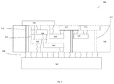
- FIG. 5 illustrates a device 500 that includes one or more embodiments of the invention.
- the device 500 may include interposer 501 , which may comprise an intervening substrate used to bridge a first substrate 502 to a second substrate 504 .
- the first substrate 502 may be, for instance, an integrated circuit die, and may or may not include embodiments of the self-aligned via described structures herein.
- the second substrate 504 may be, for instance, a memory module, a computer motherboard, or another integrated circuit die, and may or may not include embodiments of the self-aligned via described structures herein.
- the purpose of an interposer 501 is to spread a connection to a wider pitch or to reroute a connection to a different connection.
- an interposer 501 may couple an integrated circuit die to a ball grid array (BGA) 706 that can subsequently be coupled to the second substrate 504 .
- BGA ball grid array
- the first and second substrates 502 / 504 are attached to opposing sides of the interposer 501 .
- the first and second substrates 502 / 504 are attached to the same side of the interposer 501 .
- three or more substrates are interconnected by way of the interposer 501 .
- the interposer 501 may be formed of an epoxy resin, a fiberglass-reinforced epoxy resin, a ceramic material, or a polymer material such as polyimide. In further implementations, the interposer may be formed of alternate rigid or flexible materials that may include the same materials described above for use in a semiconductor substrate, such as silicon, germanium, and other group III-V and group IV materials.
- the interposer may include metal interconnects 508 and vias 510 , including but not limited to through-silicon vias (TSVs) 512 .
- TSVs through-silicon vias
- the interposer 501 may further include embedded devices 514 , including both passive and active devices.
- Such devices include, but are not limited to, capacitors, decoupling capacitors, resistors, inductors, fuses, diodes, transformers, sensors, and electrostatic discharge (ESD) devices. More complex devices such as radio-frequency (RF) devices, power amplifiers, power management devices, antennas, arrays, sensors, and MEMS devices may also be formed on the interposer 501 . In accordance with embodiments, apparatuses or processes disclosed herein may be used in the fabrication of interposer 501 .
- RF radio-frequency
- apparatuses or processes disclosed herein may be used in the fabrication of interposer 501 .
- FIG. 6 is a schematic of a computing device 600 according to an embodiment.
- the computing device 600 houses a board 602 , such as a motherboard 602 for example.
- the board 602 may include a number of components, including but not limited to a processor 604 , and an on-die memory 806 , that may be communicatively coupled with an integrated circuit die 603 , and at least one communication chip 608 .
- the processor 604 may be physically and electrically coupled to the board 602 .
- the at least one communication chip 608 may be physically and electrically coupled to the board 602 .
- the communication chip 606 is part of the processor 604 .
- computing device 600 may include other components that may or may not be physically and electrically coupled to the board 602 , and may or may not be communicatively coupled to each other. These other components include, but are not limited to, volatile memory (e.g., DRAM) 610 , non-volatile memory (e.g., ROM) 612 , flash memory (not shown), a graphics processor unit (GPU) 614 , a digital signal processor (DSP) 616 , a crypto processor 642 , a chipset 820 , an antenna 622 , a display 624 such as a touchscreen display, a touchscreen controller 626 , a battery 628 , an audio codec (not shown), a video codec (not shown), a global positioning system (GPS) device 629 , a compass 630 , accelerometer, a gyroscope and other inertial sensors 632 , a speaker 634 , a camera 636 , and a mass storage device (
- volatile memory
- the communication chip 608 enables wireless and/or wired communications for the transfer of data to and from the computing device 600 .
- wireless and its derivatives may be used to describe circuits, devices, systems, methods, techniques, communications channels, etc., that may communicate data through the use of modulated electromagnetic radiation through a non-solid medium. The term does not imply that the associated devices do not contain any wires, although in some embodiments they might not.
- the communication chip 608 may implement any of a number of wireless or wired standards or protocols, including but not limited to Wi-Fi (IEEE 802.11 family), WiMAX (IEEE 802.16 family), IEEE 802.20, long term evolution (LTE), Ev-DO, HSPA+, HSDPA+, HSUPA+, EDGE, GSM, GPRS, CDMA, TDMA, DECT, Bluetooth, Ethernet derivatives thereof, as well as any other wireless and wired protocols that are designated as 3G, 4G, 5G, and beyond.
- the computing device 600 may include a plurality of communication chips 608 .
- a first communication chip may be dedicated to shorter range wireless communications such as Wi-Fi and Bluetooth and a second communication chip may be dedicated to longer range wireless communications such as GPS, EDGE, GPRS, CDMA, WiMAX, LTE, Ev-DO, and others.
- the term “processor” may refer to any device or portion of a device that processes electronic data from registers and/or memory to transform that electronic data into other electronic data that may be stored in registers and/or memory.
- the computing device 600 may be a laptop, a netbook, a notebook, an ultrabook, a smartphone, a tablet, a personal digital assistant (PDA), an ultra mobile PC, a wearable device, a mobile phone, a desktop computer, a server, a printer, a scanner, a monitor, a set-top box, an entertainment control unit, a digital camera, a portable music player, or a digital video recorder.
- the computing device 600 may be any other electronic device that processes data.
- Embodiments may be implemented as a part of one or more memory chips, controllers, CPUs (Central Processing Unit), microchips or integrated circuits interconnected using a motherboard, an application specific integrated circuit (ASIC), and/or a field programmable gate array (FPGA).
- CPUs Central Processing Unit
- ASIC application specific integrated circuit
- FPGA field programmable gate array
- Example 1 is a microelectronic structure comprising a substrate, wherein the substrate comprises silicon; a fin comprising a first portion and a second portion; and a dopant species, wherein the first portion comprises a first dopant species concentration, and the second portion comprises a second dopant species, wherein the first dopant species concentration is substantially less than the second dopant species concentration.
- Example 2 the structure of Example 1 including wherein the dopant species comprises one of a p type or an n type dopant species.
- Example 3 the structure of Example 1 including wherein the first portion comprises a first adjacent dielectric material, and the second portion comprises a second dielectric material, wherein the second dielectric material comprises a dopant concentration about an order of magnitude greater than the first dielectric material.
- Example 4 the structure of Example 1 including wherein the structure comprises a portion of a non-planar transistor structure.
- Example 5 the structure of Example 1 including wherein the structure comprises a portion of a lightly doped channel ti-gate transistor.
- Example 6 the structure of Example 1 including wherein the dopant concentration of the first portion is about an order of magnitude less than the dopant concentration of the second portion.
- Example 7 the structure of Example 1 including wherein the fin comprises a silicon fin structure.
- Example 8 the structure of Example 1 further comprising a gate electrode adjacent a source/drain region, wherein the gate electrode is on a portion of the fin.
- Example 9 is a method comprising: providing a free standing fin on a substrate, wherein the free standing fin comprises a first portion and a second portion, wherein the first portion does not comprise an adjacent dielectric material, and wherein the second portion comprises an adjacent dielectric material; and
- Example 10 The method of Example 9 further comprising wherein the dopant species scatter out of the first portion of the fin during the implanting.
- Example 11 the method of Example 9 wherein the dopant species scatter from the dielectric material adjacent the second portion into the second portion of the free standing fin.
- Example 12 the structure of Example 9 wherein the first portion comprises a lower dopant concentration of the dopant species than the second portion.
- Example 13 the method of Example 9 wherein the fin structure is annealed.
- Example 14 the structure of Example 13 further comprising wherein the first portion comprises a cap on a top surface of the first portion.
- Example 15 the method of Example 13 wherein the dopant species in the first portion evaporate from the first portion.
- Example 16 the method of Example 13 further comprising wherein the dopants in the dielectric adjacent the second portion are diffused into the sub fin portion.
- Example 17 is a method of forming a microelectronic structure, comprising: providing a substrate, wherein the substrate comprises silicon; forming a free standing fin on the substrate, wherein the free standing fin comprises a first portion and a second portion; forming a blocking material on the first portion; forming a dopant material on the second portion; and annealing the free standing fin.
- Example 18 the method of Example 17 further comprising wherein the blocking material is selectively formed on the first portion.
- Example 19 the method of Example 18 further comprising wherein the blocking material is removed from the free standing fin subsequent to the annealing.
- Example 20 the method of Example 17 wherein a dielectric material is formed adjacent the second portion of the free standing fin subsequent to the annealing.
- Example 21 the method of Example 17 further comprising wherein the second portion comprises a higher dopant concentration than the first portion of the free standing fin.
- Example 22 the method of Example 17, further comprising wherein the dopant material comprises a dopant species that is selected from the group consisting of boron, phosphorus, arsenic and phosphorus.
- Example 23 the method of Example 17 further comprising wherein the free standing fin comprises a portion of one of a FINFET, a tri-gate, or a planar transistor structure.
- Example 24 the method of Example 17 further comprising wherein the free standing fin comprises a gate electrode adjacent to the free standing fin.
Landscapes
- Thin Film Transistor (AREA)
- Metal-Oxide And Bipolar Metal-Oxide Semiconductor Integrated Circuits (AREA)
- Insulated Gate Type Field-Effect Transistor (AREA)
Abstract
Description
Claims (17)
Applications Claiming Priority (1)
| Application Number | Priority Date | Filing Date | Title |
|---|---|---|---|
| PCT/US2015/052306 WO2017052612A1 (en) | 2015-09-25 | 2015-09-25 | Methods of doping fin structures of non-planar transistor devices |
Related Parent Applications (1)
| Application Number | Title | Priority Date | Filing Date |
|---|---|---|---|
| PCT/US2015/052306 A-371-Of-International WO2017052612A1 (en) | 2015-09-25 | 2015-09-25 | Methods of doping fin structures of non-planar transistor devices |
Related Child Applications (1)
| Application Number | Title | Priority Date | Filing Date |
|---|---|---|---|
| US16/412,305 Continuation US11264453B2 (en) | 2015-09-25 | 2019-05-14 | Methods of doping fin structures of non-planar transistor devices |
Publications (2)
| Publication Number | Publication Date |
|---|---|
| US20180254320A1 US20180254320A1 (en) | 2018-09-06 |
| US11222947B2 true US11222947B2 (en) | 2022-01-11 |
Family
ID=58386926
Family Applications (2)
| Application Number | Title | Priority Date | Filing Date |
|---|---|---|---|
| US15/757,251 Active US11222947B2 (en) | 2015-09-25 | 2015-09-25 | Methods of doping fin structures of non-planar transistor devices |
| US16/412,305 Active US11264453B2 (en) | 2015-09-25 | 2019-05-14 | Methods of doping fin structures of non-planar transistor devices |
Family Applications After (1)
| Application Number | Title | Priority Date | Filing Date |
|---|---|---|---|
| US16/412,305 Active US11264453B2 (en) | 2015-09-25 | 2019-05-14 | Methods of doping fin structures of non-planar transistor devices |
Country Status (4)
| Country | Link |
|---|---|
| US (2) | US11222947B2 (en) |
| DE (1) | DE112015006974T5 (en) |
| TW (1) | TWI713573B (en) |
| WO (1) | WO2017052612A1 (en) |
Families Citing this family (2)
| Publication number | Priority date | Publication date | Assignee | Title |
|---|---|---|---|---|
| US10720502B2 (en) * | 2018-10-22 | 2020-07-21 | International Business Machines Corporation | Vertical transistors having a layer of charge carriers in the extension region for reduced extension region resistance |
| US12469696B2 (en) * | 2021-09-01 | 2025-11-11 | Tokyo Electron Limited | Method of forming 3-dimensional spacer |
Citations (82)
| Publication number | Priority date | Publication date | Assignee | Title |
|---|---|---|---|---|
| US6475890B1 (en) | 2001-02-12 | 2002-11-05 | Advanced Micro Devices, Inc. | Fabrication of a field effect transistor with an upside down T-shaped semiconductor pillar in SOI technology |
| US6562665B1 (en) | 2000-10-16 | 2003-05-13 | Advanced Micro Devices, Inc. | Fabrication of a field effect transistor with a recess in a semiconductor pillar in SOI technology |
| US20030193058A1 (en) | 2002-04-12 | 2003-10-16 | International Business Machines Corporation | Integrated circuit with capacitors having fin structure |
| US20040256683A1 (en) | 2003-06-20 | 2004-12-23 | Deok-Hyung Lee | Integrated circuit field effect transistors including channel-containing fin having regions of high and low doping concentrations and methods of fabricating same |
| US20050019993A1 (en) | 2003-07-24 | 2005-01-27 | Deok-Hyung Lee | Methods for fabricating fin field effect transistors using a protective layer to reduce etching damage |
| US20050161739A1 (en) | 2004-01-28 | 2005-07-28 | International Business Machines Corporation | Method and structure to create multiple device widths in finfet technology in both bulk and soi |
| WO2005079182A2 (en) | 2004-01-22 | 2005-09-01 | International Business Machines Corporation | Vertical fin-fet mos devices |
| US20060244051A1 (en) | 2005-04-27 | 2006-11-02 | Kabushiki Kaisha Toshiba | Semiconductor manufacturing method and semiconductor device |
| CN1881614A (en) | 2005-02-04 | 2006-12-20 | 株式会社东芝 | Mosfet-type semiconductor device, and method of manufacturing the same |
| US20070170474A1 (en) | 2006-01-24 | 2007-07-26 | Kabushiki Kaisha Toshiba | Semiconductor device and method of fabricating the same |
| US20080111185A1 (en) * | 2006-11-13 | 2008-05-15 | International Business Machines Corporation | Asymmetric multi-gated transistor and method for forming |
| US20080149984A1 (en) | 2006-12-22 | 2008-06-26 | Chang Peter L D | Floating body memory cell having gates favoring different conductivity type regions |
| US20080296632A1 (en) | 2007-05-30 | 2008-12-04 | Synopsys, Inc. | Stress-Enhanced Performance Of A FinFet Using Surface/Channel Orientations And Strained Capping Layers |
| TW200905875A (en) | 2007-07-31 | 2009-02-01 | Taiwan Semiconductor Mfg | Method of fabrication of a FinFET element |
| US20090095980A1 (en) | 2007-10-16 | 2009-04-16 | Chen-Hua Yu | Reducing Resistance in Source and Drain Regions of FinFETs |
| US20090101978A1 (en) | 2007-10-17 | 2009-04-23 | Anderson Brent A | Fin-type field effect transistor structure with merged source/drain silicide and method of forming the structure |
| US20100052059A1 (en) | 2008-08-28 | 2010-03-04 | Taiwan Semiconductor Manufacturing Company, Ltd. | Finfet process compatible native transistor |
| US20100183961A1 (en) | 2009-01-20 | 2010-07-22 | Taiwan Semiconductor Manufacturing Company, Ltd. | Integrated circuit layout design |
| US20100203734A1 (en) | 2009-02-12 | 2010-08-12 | Taiwan Semiconductor Manufacturing Company, Ltd. | Method of pitch halving |
| US20100264497A1 (en) | 2009-04-21 | 2010-10-21 | International Business Machines Corporation | Multiple Vt Field-Effect Transistor Devices |
| US20100264468A1 (en) | 2009-04-17 | 2010-10-21 | Taiwan Semiconductor Manufacturing Company, Ltd. | Method Of Fabrication Of A FinFET Element |
| KR20110025075A (en) | 2009-09-01 | 2011-03-09 | 타이완 세미콘덕터 매뉴팩쳐링 컴퍼니 리미티드 | Accumulated fin field effect transistors, circuits and methods of manufacturing the same |
| US20110115031A1 (en) | 2006-03-22 | 2011-05-19 | Samsung Electronics Co., Ltd. | Semiconductor integrated circuit device and related method |
| US20110129990A1 (en) | 2009-11-30 | 2011-06-02 | Applied Materials, Inc. | Method for doping non-planar transistors |
| US20110171795A1 (en) | 2010-01-12 | 2011-07-14 | Taiwan Semiconductor Manufacturing Company, Ltd. | FinFET LDD and Source Drain Implant Technique |
| US20110278676A1 (en) | 2010-05-14 | 2011-11-17 | Taiwan Semiconductor Manufacturing Company, Ltd. | Method and apparatus for enhancing channel strain |
| US20110317485A1 (en) | 2010-06-25 | 2011-12-29 | Taiwan Semiconductor Manufacturing Company, Ltd. | Structure and method for sram cell circuit |
| US20120012932A1 (en) | 2010-07-15 | 2012-01-19 | Taiwan Semiconductor Manufacturing Company, Ltd. | Fin-like field effect transistor (finfet) device and method of manufacturing same |
| US20120104472A1 (en) | 2010-10-18 | 2012-05-03 | Taiwan Semiconductor Manufacturing Company, Ltd. | Fin-like field effect transistor (finfet) device and method of manufacturing same |
| US20120326219A1 (en) * | 2011-06-21 | 2012-12-27 | Nicky Lu | Dynamic memory structure |
| US20130043563A1 (en) | 2011-08-19 | 2013-02-21 | Keisuke Nakazawa | Semiconductor device and method of manufacturing the same |
| US20130043536A1 (en) | 2011-08-19 | 2013-02-21 | Irfan Rahim | Buffered finfet device |
| US20130102137A1 (en) | 2011-10-25 | 2013-04-25 | Taiwan Semiconductor Manufacturing Company, Ltd., ("Tsmc") | Doping method in 3d semiconductor device |
| US20130119482A1 (en) | 2011-11-10 | 2013-05-16 | Taiwan Semiconductor Manufacturing Company, Ltd. | Fin field effect transistors and methods for fabricating the same |
| US20130126951A1 (en) | 2009-09-29 | 2013-05-23 | Taiwan Semiconductor Manufacturing Company, Ltd. | Method of Fabricating FinFET Device and Structure Thereof |
| US20130244392A1 (en) | 2012-03-19 | 2013-09-19 | Samsung Electronics Co., Ltd. | Method of fabricating fin-field effect transistors (finfets) having different fin widths |
| US20130285153A1 (en) | 2012-04-25 | 2013-10-31 | Taiwan Semiconductor Manufacturing Company Ltd. | Strained structure of semiconductor device and method of making the strained structure |
| US20130307088A1 (en) | 2012-05-18 | 2013-11-21 | Taiwan Semiconductor Manufacturing Company, Ltd., ("Tsmc") | Metal gate finfet device and method of fabricating thereof |
| US20130328134A1 (en) | 2010-09-27 | 2013-12-12 | Taiwan Semiconductor Manufacturing Company, Ltd. | Method and Apparatus for Improving Gate Contact |
| US20130334616A1 (en) | 2011-09-28 | 2013-12-19 | GLOBALFOUNDRIER Singapore Pte. Ltd. | Reliable contacts |
| US20140061820A1 (en) | 2012-09-06 | 2014-03-06 | International Business Machines Corporation | Bulk finfet with controlled fin height and high-k liner |
| US20140065782A1 (en) | 2012-08-30 | 2014-03-06 | Chih Wei Lu | Method of making a finfet device |
| US20140103450A1 (en) | 2012-10-12 | 2014-04-17 | International Business Machines Corporation | Hybrid orientation fin field effect transistor and planar field effect transistor |
| US20140191318A1 (en) | 2013-01-10 | 2014-07-10 | United Microelectronics Corp. | Complementary metal oxide semiconductor field effect transistor, metal oxide semiconductor field effect transistor and manufacturing method thereof |
| US20140199849A1 (en) | 2013-01-17 | 2014-07-17 | Applied Materials, Inc. | Polysilicon over-etch using hydrogen diluted plasma for three-dimensional gate etch |
| US20140239347A1 (en) | 2013-02-27 | 2014-08-28 | Taiwan Semiconductor Manufacturing Company, Ltd. | Structure and Method for Defect Passivation To Reduce Junction Leakage For FinFET Device |
| US20140264485A1 (en) | 2013-03-15 | 2014-09-18 | Qualcomm Incorporated | Fin-type semiconductor device |
| WO2014204477A1 (en) | 2013-06-20 | 2014-12-24 | Intel Corporation | Non-planar semiconductor device having doped sub-fin region and method to fabricate same |
| US20150021710A1 (en) | 2013-07-19 | 2015-01-22 | Taiwan Semiconductor Manufacturing Company, Ltd. | Methods for Forming STI Regions in Integrated Circuits |
| US20150054089A1 (en) | 2013-08-22 | 2015-02-26 | Samsung Electronics Co., Ltd. | Semiconductor devices having 3d channels, and methods of fabricating semiconductor devices having 3d channels |
| US20150069474A1 (en) * | 2013-09-11 | 2015-03-12 | Taiwan Semiconductor Manufacturing Company, Ltd. | Isolation Structure of Fin Field Effect Transistor |
| US20150079752A1 (en) | 2011-09-06 | 2015-03-19 | Taiwan Semiconductor Manufacturing Company, Ltd. | FinFET Design Controlling Channel Thickness |
| US20150155383A1 (en) | 2013-12-04 | 2015-06-04 | Taiwan Semiconductor Manufacturing Company, Ltd. | Semiconductor Device with Strained Layer |
| US20150243784A1 (en) | 2014-02-21 | 2015-08-27 | Stmicroelectronics, Inc. | Method to form strained channel in thin box soi structures by elastic strain relaxation of the substrate |
| US20150279933A1 (en) * | 2014-03-27 | 2015-10-01 | Semiconductor Manufacturing International (Shanghai) Corporation | Fin-type field effect transistor and manufacturing method thereof |
| US20150279995A1 (en) | 2014-03-26 | 2015-10-01 | Shigenobu Maeda | Semiconductor devices and methods of fabricating the same |
| US20150303218A1 (en) | 2014-04-16 | 2015-10-22 | Commissariat à l'énergie atomique et aux énergies alternatives | Method to co-integrate oppositely strained semiconductor devices on a same substrate |
| US20150364579A1 (en) | 2014-06-12 | 2015-12-17 | Taiwan Semiconductor Manufacturing Co., Ltd | Structure and formation method of fin-like field effect transistor |
| US20150364580A1 (en) | 2014-06-12 | 2015-12-17 | Taiwan Semiconductor Manufacturing Co., Ltd. | Structure and formation method of fin-like field effect transistor |
| US20150364593A1 (en) | 2014-06-12 | 2015-12-17 | Taiwan Semiconductor Manufacturing Co., Ltd. | Structure and formation method of fin-like field effect transistor |
| US20150372139A1 (en) | 2014-06-18 | 2015-12-24 | GLOBALFOUNDERS Inc. | Constraining epitaxial growth on fins of a finfet device |
| US20160020210A1 (en) | 2014-07-18 | 2016-01-21 | Taiwan Semiconductor Manufacturing Company, Ltd | Structure and method for mosfet device |
| US20160043225A1 (en) | 2014-08-05 | 2016-02-11 | Taiwan Semiconductor Manufacturing Company, Ltd. | Nonplanar Device and Strain-Generating Channel Dielectric |
| US20160087053A1 (en) | 2014-09-23 | 2016-03-24 | Jin-Bum Kim | Semiconductor device and method of fabricating the same |
| US20160099245A1 (en) | 2014-10-02 | 2016-04-07 | International Business Machines Corporation | Semiconductor devices with sidewall spacers of equal thickness |
| US20160104776A1 (en) | 2014-10-10 | 2016-04-14 | Taiwan Semiconductor Manufacturing Company, Ltd. | High Mobility Devices with Anti-Punch Through Layer and Methods of Forming Same |
| US20160111336A1 (en) | 2014-10-17 | 2016-04-21 | Taiwan Semiconductor Manufacturing Company, Ltd. | Method and Structure for FinFET Isolation |
| US20160163604A1 (en) | 2014-12-05 | 2016-06-09 | Globalfoundries Inc. | Methods of forming diffusion breaks on integrated circuit products comprised of finfet devices and the resulting products |
| US20160181247A1 (en) | 2014-12-18 | 2016-06-23 | International Business Machines Corporation | Field-isolated bulk finfet |
| US20160181366A1 (en) | 2012-03-21 | 2016-06-23 | Samsung Electronics Co., Ltd. | Field effect transistors including fin structures with different doped regions and semiconductor devices including the same |
| US20160181360A1 (en) | 2014-12-19 | 2016-06-23 | Taiwan Semiconductor Manufacturing Co., Ltd | Semiconductor structure with etched fin structure and method for forming the same |
| US20160190137A1 (en) | 2014-12-26 | 2016-06-30 | Taiwan Semiconductor Manufacturing Company Ltd. | Finfet structure and method for manufacturing thereof |
| US20160190306A1 (en) | 2013-11-13 | 2016-06-30 | Globalfoundries Inc. | Finfet device with a substantially self-aligned isolation region positioned under the channel region |
| US9390981B1 (en) | 2015-02-05 | 2016-07-12 | Globalfoundries Inc. | Method of forming a complementary metal oxide semiconductor structure with N-type and P-type field effect transistors having symmetric source/drain junctions and optional dual silicides |
| US20160204215A1 (en) | 2015-01-12 | 2016-07-14 | Taiwan Semiconductor Manufacturing Co., Ltd. | Semiconductor device and manufacturing method thereof |
| US20160211326A1 (en) * | 2015-01-20 | 2016-07-21 | Taiwan Semiconductor Manufacturing Company Ltd. | Finfet structure and method for manufacturing thereof |
| US9543382B1 (en) | 2015-03-19 | 2017-01-10 | Altera Corporation | FinFET with improved SEU performance |
| US20170062427A1 (en) | 2015-08-25 | 2017-03-02 | International Business Machines Corporation | Method and structure for forming finfet cmos with dual doped sti regions |
| US20170213835A1 (en) | 2014-12-23 | 2017-07-27 | International Business Machines Corporation | Semiconductor structures with deep trench capacitor and methods of manufacture |
| US20170229578A1 (en) | 2016-02-09 | 2017-08-10 | Globalfoundries Inc. | Device with diffusion blocking layer in source/drain region |
| US20180053761A1 (en) | 2016-08-21 | 2018-02-22 | United Microelectronics Corp. | Semiconductor device and manufacturing method thereof |
| US20180158811A1 (en) | 2016-12-07 | 2018-06-07 | Samsung Electronics Co., Ltd. | Integrated circuit devices |
-
2015
- 2015-09-25 DE DE112015006974.7T patent/DE112015006974T5/en active Pending
- 2015-09-25 WO PCT/US2015/052306 patent/WO2017052612A1/en not_active Ceased
- 2015-09-25 US US15/757,251 patent/US11222947B2/en active Active
-
2016
- 2016-08-23 TW TW105126926A patent/TWI713573B/en active
-
2019
- 2019-05-14 US US16/412,305 patent/US11264453B2/en active Active
Patent Citations (92)
| Publication number | Priority date | Publication date | Assignee | Title |
|---|---|---|---|---|
| US6562665B1 (en) | 2000-10-16 | 2003-05-13 | Advanced Micro Devices, Inc. | Fabrication of a field effect transistor with a recess in a semiconductor pillar in SOI technology |
| US6475890B1 (en) | 2001-02-12 | 2002-11-05 | Advanced Micro Devices, Inc. | Fabrication of a field effect transistor with an upside down T-shaped semiconductor pillar in SOI technology |
| US20030193058A1 (en) | 2002-04-12 | 2003-10-16 | International Business Machines Corporation | Integrated circuit with capacitors having fin structure |
| US20040256683A1 (en) | 2003-06-20 | 2004-12-23 | Deok-Hyung Lee | Integrated circuit field effect transistors including channel-containing fin having regions of high and low doping concentrations and methods of fabricating same |
| US20050019993A1 (en) | 2003-07-24 | 2005-01-27 | Deok-Hyung Lee | Methods for fabricating fin field effect transistors using a protective layer to reduce etching damage |
| WO2005079182A2 (en) | 2004-01-22 | 2005-09-01 | International Business Machines Corporation | Vertical fin-fet mos devices |
| US20070134864A1 (en) | 2004-01-28 | 2007-06-14 | Anderson Brent A | Method and structure to create multiple device widths in finfet technology in both bulk and soi |
| US20050161739A1 (en) | 2004-01-28 | 2005-07-28 | International Business Machines Corporation | Method and structure to create multiple device widths in finfet technology in both bulk and soi |
| US7420230B2 (en) | 2005-02-04 | 2008-09-02 | Kabushiki Kaisha Toshiba | MOSFET-type semiconductor device, and method of manufacturing the same |
| CN1881614A (en) | 2005-02-04 | 2006-12-20 | 株式会社东芝 | Mosfet-type semiconductor device, and method of manufacturing the same |
| US20060244051A1 (en) | 2005-04-27 | 2006-11-02 | Kabushiki Kaisha Toshiba | Semiconductor manufacturing method and semiconductor device |
| US20070170474A1 (en) | 2006-01-24 | 2007-07-26 | Kabushiki Kaisha Toshiba | Semiconductor device and method of fabricating the same |
| JP2007201021A (en) | 2006-01-24 | 2007-08-09 | Toshiba Corp | Semiconductor device |
| US20110115031A1 (en) | 2006-03-22 | 2011-05-19 | Samsung Electronics Co., Ltd. | Semiconductor integrated circuit device and related method |
| US20080111185A1 (en) * | 2006-11-13 | 2008-05-15 | International Business Machines Corporation | Asymmetric multi-gated transistor and method for forming |
| US8679906B2 (en) | 2006-11-13 | 2014-03-25 | International Business Machines Corporation | Asymmetric multi-gated transistor and method for forming |
| CN101183686A (en) | 2006-11-13 | 2008-05-21 | 国际商业机器公司 | Asymmetric multi-gate transistor and method of forming same |
| US20080149984A1 (en) | 2006-12-22 | 2008-06-26 | Chang Peter L D | Floating body memory cell having gates favoring different conductivity type regions |
| US20080296632A1 (en) | 2007-05-30 | 2008-12-04 | Synopsys, Inc. | Stress-Enhanced Performance Of A FinFet Using Surface/Channel Orientations And Strained Capping Layers |
| TW200905875A (en) | 2007-07-31 | 2009-02-01 | Taiwan Semiconductor Mfg | Method of fabrication of a FinFET element |
| US8883597B2 (en) | 2007-07-31 | 2014-11-11 | Taiwan Semiconductor Manufacturing Company, Ltd. | Method of fabrication of a FinFET element |
| US20090095980A1 (en) | 2007-10-16 | 2009-04-16 | Chen-Hua Yu | Reducing Resistance in Source and Drain Regions of FinFETs |
| US20090101978A1 (en) | 2007-10-17 | 2009-04-23 | Anderson Brent A | Fin-type field effect transistor structure with merged source/drain silicide and method of forming the structure |
| US20100052059A1 (en) | 2008-08-28 | 2010-03-04 | Taiwan Semiconductor Manufacturing Company, Ltd. | Finfet process compatible native transistor |
| US20100183961A1 (en) | 2009-01-20 | 2010-07-22 | Taiwan Semiconductor Manufacturing Company, Ltd. | Integrated circuit layout design |
| US20100203734A1 (en) | 2009-02-12 | 2010-08-12 | Taiwan Semiconductor Manufacturing Company, Ltd. | Method of pitch halving |
| US20100264468A1 (en) | 2009-04-17 | 2010-10-21 | Taiwan Semiconductor Manufacturing Company, Ltd. | Method Of Fabrication Of A FinFET Element |
| US20100264497A1 (en) | 2009-04-21 | 2010-10-21 | International Business Machines Corporation | Multiple Vt Field-Effect Transistor Devices |
| KR20110025075A (en) | 2009-09-01 | 2011-03-09 | 타이완 세미콘덕터 매뉴팩쳐링 컴퍼니 리미티드 | Accumulated fin field effect transistors, circuits and methods of manufacturing the same |
| US8264032B2 (en) | 2009-09-01 | 2012-09-11 | Taiwan Semiconductor Manufacturing Company, Ltd. | Accumulation type FinFET, circuits and fabrication method thereof |
| US20130126951A1 (en) | 2009-09-29 | 2013-05-23 | Taiwan Semiconductor Manufacturing Company, Ltd. | Method of Fabricating FinFET Device and Structure Thereof |
| US20110129990A1 (en) | 2009-11-30 | 2011-06-02 | Applied Materials, Inc. | Method for doping non-planar transistors |
| US20110171795A1 (en) | 2010-01-12 | 2011-07-14 | Taiwan Semiconductor Manufacturing Company, Ltd. | FinFET LDD and Source Drain Implant Technique |
| US20110278676A1 (en) | 2010-05-14 | 2011-11-17 | Taiwan Semiconductor Manufacturing Company, Ltd. | Method and apparatus for enhancing channel strain |
| US20110317485A1 (en) | 2010-06-25 | 2011-12-29 | Taiwan Semiconductor Manufacturing Company, Ltd. | Structure and method for sram cell circuit |
| US20120012932A1 (en) | 2010-07-15 | 2012-01-19 | Taiwan Semiconductor Manufacturing Company, Ltd. | Fin-like field effect transistor (finfet) device and method of manufacturing same |
| US20130328134A1 (en) | 2010-09-27 | 2013-12-12 | Taiwan Semiconductor Manufacturing Company, Ltd. | Method and Apparatus for Improving Gate Contact |
| US20120104472A1 (en) | 2010-10-18 | 2012-05-03 | Taiwan Semiconductor Manufacturing Company, Ltd. | Fin-like field effect transistor (finfet) device and method of manufacturing same |
| US20120326219A1 (en) * | 2011-06-21 | 2012-12-27 | Nicky Lu | Dynamic memory structure |
| US20130043536A1 (en) | 2011-08-19 | 2013-02-21 | Irfan Rahim | Buffered finfet device |
| US20130043563A1 (en) | 2011-08-19 | 2013-02-21 | Keisuke Nakazawa | Semiconductor device and method of manufacturing the same |
| US20150079752A1 (en) | 2011-09-06 | 2015-03-19 | Taiwan Semiconductor Manufacturing Company, Ltd. | FinFET Design Controlling Channel Thickness |
| US20130334616A1 (en) | 2011-09-28 | 2013-12-19 | GLOBALFOUNDRIER Singapore Pte. Ltd. | Reliable contacts |
| US20130102137A1 (en) | 2011-10-25 | 2013-04-25 | Taiwan Semiconductor Manufacturing Company, Ltd., ("Tsmc") | Doping method in 3d semiconductor device |
| US20130119482A1 (en) | 2011-11-10 | 2013-05-16 | Taiwan Semiconductor Manufacturing Company, Ltd. | Fin field effect transistors and methods for fabricating the same |
| US20130244392A1 (en) | 2012-03-19 | 2013-09-19 | Samsung Electronics Co., Ltd. | Method of fabricating fin-field effect transistors (finfets) having different fin widths |
| US20160181366A1 (en) | 2012-03-21 | 2016-06-23 | Samsung Electronics Co., Ltd. | Field effect transistors including fin structures with different doped regions and semiconductor devices including the same |
| US20130285153A1 (en) | 2012-04-25 | 2013-10-31 | Taiwan Semiconductor Manufacturing Company Ltd. | Strained structure of semiconductor device and method of making the strained structure |
| US20130307088A1 (en) | 2012-05-18 | 2013-11-21 | Taiwan Semiconductor Manufacturing Company, Ltd., ("Tsmc") | Metal gate finfet device and method of fabricating thereof |
| US20140065782A1 (en) | 2012-08-30 | 2014-03-06 | Chih Wei Lu | Method of making a finfet device |
| US20140061820A1 (en) | 2012-09-06 | 2014-03-06 | International Business Machines Corporation | Bulk finfet with controlled fin height and high-k liner |
| US20140103450A1 (en) | 2012-10-12 | 2014-04-17 | International Business Machines Corporation | Hybrid orientation fin field effect transistor and planar field effect transistor |
| US20140191318A1 (en) | 2013-01-10 | 2014-07-10 | United Microelectronics Corp. | Complementary metal oxide semiconductor field effect transistor, metal oxide semiconductor field effect transistor and manufacturing method thereof |
| US20140199849A1 (en) | 2013-01-17 | 2014-07-17 | Applied Materials, Inc. | Polysilicon over-etch using hydrogen diluted plasma for three-dimensional gate etch |
| US20140239347A1 (en) | 2013-02-27 | 2014-08-28 | Taiwan Semiconductor Manufacturing Company, Ltd. | Structure and Method for Defect Passivation To Reduce Junction Leakage For FinFET Device |
| TW201434156A (en) | 2013-02-27 | 2014-09-01 | 台灣積體電路製造股份有限公司 | Semiconductor structure and method for manufacturing fin field effect transistor |
| US9184233B2 (en) | 2013-02-27 | 2015-11-10 | Taiwan Semiconductor Manufacturing Company, Ltd. | Structure and method for defect passivation to reduce junction leakage for finFET device |
| US20140264485A1 (en) | 2013-03-15 | 2014-09-18 | Qualcomm Incorporated | Fin-type semiconductor device |
| WO2014204477A1 (en) | 2013-06-20 | 2014-12-24 | Intel Corporation | Non-planar semiconductor device having doped sub-fin region and method to fabricate same |
| US20160056156A1 (en) | 2013-06-20 | 2016-02-25 | Intel Corporation | Non-planar semiconductor device having doped sub-fin region and method to fabricate same |
| US20150021710A1 (en) | 2013-07-19 | 2015-01-22 | Taiwan Semiconductor Manufacturing Company, Ltd. | Methods for Forming STI Regions in Integrated Circuits |
| US20150054089A1 (en) | 2013-08-22 | 2015-02-26 | Samsung Electronics Co., Ltd. | Semiconductor devices having 3d channels, and methods of fabricating semiconductor devices having 3d channels |
| US20150069474A1 (en) * | 2013-09-11 | 2015-03-12 | Taiwan Semiconductor Manufacturing Company, Ltd. | Isolation Structure of Fin Field Effect Transistor |
| US20160190306A1 (en) | 2013-11-13 | 2016-06-30 | Globalfoundries Inc. | Finfet device with a substantially self-aligned isolation region positioned under the channel region |
| US20150155383A1 (en) | 2013-12-04 | 2015-06-04 | Taiwan Semiconductor Manufacturing Company, Ltd. | Semiconductor Device with Strained Layer |
| US20150243784A1 (en) | 2014-02-21 | 2015-08-27 | Stmicroelectronics, Inc. | Method to form strained channel in thin box soi structures by elastic strain relaxation of the substrate |
| US20150279995A1 (en) | 2014-03-26 | 2015-10-01 | Shigenobu Maeda | Semiconductor devices and methods of fabricating the same |
| US20150279933A1 (en) * | 2014-03-27 | 2015-10-01 | Semiconductor Manufacturing International (Shanghai) Corporation | Fin-type field effect transistor and manufacturing method thereof |
| US20150303218A1 (en) | 2014-04-16 | 2015-10-22 | Commissariat à l'énergie atomique et aux énergies alternatives | Method to co-integrate oppositely strained semiconductor devices on a same substrate |
| US20150364593A1 (en) | 2014-06-12 | 2015-12-17 | Taiwan Semiconductor Manufacturing Co., Ltd. | Structure and formation method of fin-like field effect transistor |
| US20150364580A1 (en) | 2014-06-12 | 2015-12-17 | Taiwan Semiconductor Manufacturing Co., Ltd. | Structure and formation method of fin-like field effect transistor |
| US20150364579A1 (en) | 2014-06-12 | 2015-12-17 | Taiwan Semiconductor Manufacturing Co., Ltd | Structure and formation method of fin-like field effect transistor |
| US20150372139A1 (en) | 2014-06-18 | 2015-12-24 | GLOBALFOUNDERS Inc. | Constraining epitaxial growth on fins of a finfet device |
| US20160020210A1 (en) | 2014-07-18 | 2016-01-21 | Taiwan Semiconductor Manufacturing Company, Ltd | Structure and method for mosfet device |
| US20160043225A1 (en) | 2014-08-05 | 2016-02-11 | Taiwan Semiconductor Manufacturing Company, Ltd. | Nonplanar Device and Strain-Generating Channel Dielectric |
| US20160087053A1 (en) | 2014-09-23 | 2016-03-24 | Jin-Bum Kim | Semiconductor device and method of fabricating the same |
| US20160099245A1 (en) | 2014-10-02 | 2016-04-07 | International Business Machines Corporation | Semiconductor devices with sidewall spacers of equal thickness |
| US20160104776A1 (en) | 2014-10-10 | 2016-04-14 | Taiwan Semiconductor Manufacturing Company, Ltd. | High Mobility Devices with Anti-Punch Through Layer and Methods of Forming Same |
| US20160111336A1 (en) | 2014-10-17 | 2016-04-21 | Taiwan Semiconductor Manufacturing Company, Ltd. | Method and Structure for FinFET Isolation |
| US20160163604A1 (en) | 2014-12-05 | 2016-06-09 | Globalfoundries Inc. | Methods of forming diffusion breaks on integrated circuit products comprised of finfet devices and the resulting products |
| US20160181247A1 (en) | 2014-12-18 | 2016-06-23 | International Business Machines Corporation | Field-isolated bulk finfet |
| US20160181360A1 (en) | 2014-12-19 | 2016-06-23 | Taiwan Semiconductor Manufacturing Co., Ltd | Semiconductor structure with etched fin structure and method for forming the same |
| US20170213835A1 (en) | 2014-12-23 | 2017-07-27 | International Business Machines Corporation | Semiconductor structures with deep trench capacitor and methods of manufacture |
| US20160190137A1 (en) | 2014-12-26 | 2016-06-30 | Taiwan Semiconductor Manufacturing Company Ltd. | Finfet structure and method for manufacturing thereof |
| US20160204215A1 (en) | 2015-01-12 | 2016-07-14 | Taiwan Semiconductor Manufacturing Co., Ltd. | Semiconductor device and manufacturing method thereof |
| US20160211326A1 (en) * | 2015-01-20 | 2016-07-21 | Taiwan Semiconductor Manufacturing Company Ltd. | Finfet structure and method for manufacturing thereof |
| US9390981B1 (en) | 2015-02-05 | 2016-07-12 | Globalfoundries Inc. | Method of forming a complementary metal oxide semiconductor structure with N-type and P-type field effect transistors having symmetric source/drain junctions and optional dual silicides |
| US9543382B1 (en) | 2015-03-19 | 2017-01-10 | Altera Corporation | FinFET with improved SEU performance |
| US20170062427A1 (en) | 2015-08-25 | 2017-03-02 | International Business Machines Corporation | Method and structure for forming finfet cmos with dual doped sti regions |
| US20170229578A1 (en) | 2016-02-09 | 2017-08-10 | Globalfoundries Inc. | Device with diffusion blocking layer in source/drain region |
| US20180053761A1 (en) | 2016-08-21 | 2018-02-22 | United Microelectronics Corp. | Semiconductor device and manufacturing method thereof |
| US20180158811A1 (en) | 2016-12-07 | 2018-06-07 | Samsung Electronics Co., Ltd. | Integrated circuit devices |
Non-Patent Citations (5)
| Title |
|---|
| Final Office Action from U.S. Appl. No. 16/412,305 dated Jul. 8, 2021, 5 pgs. |
| International Search Report and Written Opinion from PCT/US2015/052306 notified Jun. 15, 2016, 13 pgs. |
| Notice of Allowance from Taiwan Patent Application No. 105126926 dated Sep. 4, 2020, 3 pgs. |
| Office Action from Taiwan Patent Application No. 105126926 dated Jan. 15, 2020, 15 pgs. |
| Restriction Requirement from U.S. Appl. No. 16/412,305 dated Aug. 6, 2020, 5 pgs. |
Also Published As
| Publication number | Publication date |
|---|---|
| US11264453B2 (en) | 2022-03-01 |
| TW201724277A (en) | 2017-07-01 |
| TWI713573B (en) | 2020-12-21 |
| WO2017052612A1 (en) | 2017-03-30 |
| DE112015006974T5 (en) | 2019-01-24 |
| US20180254320A1 (en) | 2018-09-06 |
| US20190267448A1 (en) | 2019-08-29 |
Similar Documents
| Publication | Publication Date | Title |
|---|---|---|
| US10797139B2 (en) | Methods of forming backside self-aligned vias and structures formed thereby | |
| US10672868B2 (en) | Methods of forming self aligned spacers for nanowire device structures | |
| US9929273B2 (en) | Apparatus and methods of forming fin structures with asymmetric profile | |
| KR102351550B1 (en) | Apparatus and methods of forming fin structures with sidewall liner | |
| US11004978B2 (en) | Methods of forming doped source/drain contacts and structures formed thereby | |
| US11967615B2 (en) | Dual threshold voltage (VT) channel devices and their methods of fabrication | |
| US11264453B2 (en) | Methods of doping fin structures of non-planar transistor devices | |
| US11424335B2 (en) | Group III-V semiconductor devices having dual workfunction gate electrodes | |
| WO2019132943A1 (en) | Lateral epitaxial overgrowth in integrated circuits | |
| US11721766B2 (en) | Metal-assisted single crystal transistors | |
| US20240113109A1 (en) | Plug between two gates of a semiconductor device | |
| US11164747B2 (en) | Group III-V semiconductor devices having asymmetric source and drain structures | |
| US20230111323A1 (en) | Oxide layer doping on a sub channel of a transistor structure |
Legal Events
| Date | Code | Title | Description |
|---|---|---|---|
| FEPP | Fee payment procedure |
Free format text: ENTITY STATUS SET TO UNDISCOUNTED (ORIGINAL EVENT CODE: BIG.); ENTITY STATUS OF PATENT OWNER: LARGE ENTITY |
|
| STPP | Information on status: patent application and granting procedure in general |
Free format text: DOCKETED NEW CASE - READY FOR EXAMINATION |
|
| STPP | Information on status: patent application and granting procedure in general |
Free format text: NON FINAL ACTION MAILED |
|
| STPP | Information on status: patent application and granting procedure in general |
Free format text: RESPONSE TO NON-FINAL OFFICE ACTION ENTERED AND FORWARDED TO EXAMINER |
|
| STPP | Information on status: patent application and granting procedure in general |
Free format text: FINAL REJECTION MAILED |
|
| STPP | Information on status: patent application and granting procedure in general |
Free format text: NON FINAL ACTION MAILED |
|
| STPP | Information on status: patent application and granting procedure in general |
Free format text: FINAL REJECTION MAILED |
|
| STPP | Information on status: patent application and granting procedure in general |
Free format text: RESPONSE AFTER FINAL ACTION FORWARDED TO EXAMINER |
|
| STPP | Information on status: patent application and granting procedure in general |
Free format text: ADVISORY ACTION MAILED |
|
| STCV | Information on status: appeal procedure |
Free format text: NOTICE OF APPEAL FILED |
|
| STCV | Information on status: appeal procedure |
Free format text: APPEAL BRIEF (OR SUPPLEMENTAL BRIEF) ENTERED AND FORWARDED TO EXAMINER |
|
| STPP | Information on status: patent application and granting procedure in general |
Free format text: NOTICE OF ALLOWANCE MAILED -- APPLICATION RECEIVED IN OFFICE OF PUBLICATIONS |
|
| STPP | Information on status: patent application and granting procedure in general |
Free format text: AWAITING TC RESP., ISSUE FEE NOT PAID |
|
| STPP | Information on status: patent application and granting procedure in general |
Free format text: NOTICE OF ALLOWANCE MAILED -- APPLICATION RECEIVED IN OFFICE OF PUBLICATIONS |
|
| STPP | Information on status: patent application and granting procedure in general |
Free format text: PUBLICATIONS -- ISSUE FEE PAYMENT VERIFIED |
|
| STCF | Information on status: patent grant |
Free format text: PATENTED CASE |
|
| MAFP | Maintenance fee payment |
Free format text: PAYMENT OF MAINTENANCE FEE, 4TH YEAR, LARGE ENTITY (ORIGINAL EVENT CODE: M1551); ENTITY STATUS OF PATENT OWNER: LARGE ENTITY Year of fee payment: 4 |