US11222687B2 - System and method for power plane noise reduction in a memory subsystem of an information handling system - Google Patents
System and method for power plane noise reduction in a memory subsystem of an information handling system Download PDFInfo
- Publication number
- US11222687B2 US11222687B2 US16/815,191 US202016815191A US11222687B2 US 11222687 B2 US11222687 B2 US 11222687B2 US 202016815191 A US202016815191 A US 202016815191A US 11222687 B2 US11222687 B2 US 11222687B2
- Authority
- US
- United States
- Prior art keywords
- clock signal
- memory
- delay setting
- delay
- delayed clock
- Prior art date
- Legal status (The legal status is an assumption and is not a legal conclusion. Google has not performed a legal analysis and makes no representation as to the accuracy of the status listed.)
- Active
Links
Images


Classifications
-
- G—PHYSICS
- G11—INFORMATION STORAGE
- G11C—STATIC STORES
- G11C11/00—Digital stores characterised by the use of particular electric or magnetic storage elements; Storage elements therefor
- G11C11/21—Digital stores characterised by the use of particular electric or magnetic storage elements; Storage elements therefor using electric elements
- G11C11/34—Digital stores characterised by the use of particular electric or magnetic storage elements; Storage elements therefor using electric elements using semiconductor devices
- G11C11/40—Digital stores characterised by the use of particular electric or magnetic storage elements; Storage elements therefor using electric elements using semiconductor devices using transistors
- G11C11/401—Digital stores characterised by the use of particular electric or magnetic storage elements; Storage elements therefor using electric elements using semiconductor devices using transistors forming cells needing refreshing or charge regeneration, i.e. dynamic cells
- G11C11/4063—Auxiliary circuits, e.g. for addressing, decoding, driving, writing, sensing or timing
- G11C11/407—Auxiliary circuits, e.g. for addressing, decoding, driving, writing, sensing or timing for memory cells of the field-effect type
- G11C11/4076—Timing circuits
-
- G—PHYSICS
- G06—COMPUTING OR CALCULATING; COUNTING
- G06F—ELECTRIC DIGITAL DATA PROCESSING
- G06F1/00—Details not covered by groups G06F3/00 - G06F13/00 and G06F21/00
- G06F1/26—Power supply means, e.g. regulation thereof
- G06F1/32—Means for saving power
- G06F1/3203—Power management, i.e. event-based initiation of a power-saving mode
- G06F1/3234—Power saving characterised by the action undertaken
- G06F1/324—Power saving characterised by the action undertaken by lowering clock frequency
-
- G—PHYSICS
- G06—COMPUTING OR CALCULATING; COUNTING
- G06F—ELECTRIC DIGITAL DATA PROCESSING
- G06F13/00—Interconnection of, or transfer of information or other signals between, memories, input/output devices or central processing units
- G06F13/38—Information transfer, e.g. on bus
- G06F13/42—Bus transfer protocol, e.g. handshake; Synchronisation
- G06F13/4282—Bus transfer protocol, e.g. handshake; Synchronisation on a serial bus, e.g. I2C bus, SPI bus
- G06F13/4291—Bus transfer protocol, e.g. handshake; Synchronisation on a serial bus, e.g. I2C bus, SPI bus using a clocked protocol
-
- G—PHYSICS
- G11—INFORMATION STORAGE
- G11C—STATIC STORES
- G11C11/00—Digital stores characterised by the use of particular electric or magnetic storage elements; Storage elements therefor
- G11C11/21—Digital stores characterised by the use of particular electric or magnetic storage elements; Storage elements therefor using electric elements
- G11C11/34—Digital stores characterised by the use of particular electric or magnetic storage elements; Storage elements therefor using electric elements using semiconductor devices
- G11C11/40—Digital stores characterised by the use of particular electric or magnetic storage elements; Storage elements therefor using electric elements using semiconductor devices using transistors
- G11C11/401—Digital stores characterised by the use of particular electric or magnetic storage elements; Storage elements therefor using electric elements using semiconductor devices using transistors forming cells needing refreshing or charge regeneration, i.e. dynamic cells
- G11C11/4063—Auxiliary circuits, e.g. for addressing, decoding, driving, writing, sensing or timing
- G11C11/407—Auxiliary circuits, e.g. for addressing, decoding, driving, writing, sensing or timing for memory cells of the field-effect type
- G11C11/4074—Power supply or voltage generation circuits, e.g. bias voltage generators, substrate voltage generators, back-up power, power control circuits
-
- G—PHYSICS
- G11—INFORMATION STORAGE
- G11C—STATIC STORES
- G11C29/00—Checking stores for correct operation ; Subsequent repair; Testing stores during standby or offline operation
- G11C29/04—Detection or location of defective memory elements, e.g. cell constructio details, timing of test signals
- G11C29/50—Marginal testing, e.g. race, voltage or current testing
- G11C29/50012—Marginal testing, e.g. race, voltage or current testing of timing
-
- G—PHYSICS
- G11—INFORMATION STORAGE
- G11C—STATIC STORES
- G11C5/00—Details of stores covered by group G11C11/00
- G11C5/02—Disposition of storage elements, e.g. in the form of a matrix array
- G11C5/04—Supports for storage elements, e.g. memory modules; Mounting or fixing of storage elements on such supports
-
- G—PHYSICS
- G11—INFORMATION STORAGE
- G11C—STATIC STORES
- G11C5/00—Details of stores covered by group G11C11/00
- G11C5/14—Power supply arrangements, e.g. power down, chip selection or deselection, layout of wirings or power grids, or multiple supply levels
-
- G—PHYSICS
- G11—INFORMATION STORAGE
- G11C—STATIC STORES
- G11C5/00—Details of stores covered by group G11C11/00
- G11C5/14—Power supply arrangements, e.g. power down, chip selection or deselection, layout of wirings or power grids, or multiple supply levels
- G11C5/143—Detection of memory cassette insertion or removal; Continuity checks of supply or ground lines; Detection of supply variations, interruptions or levels ; Switching between alternative supplies
-
- G—PHYSICS
- G11—INFORMATION STORAGE
- G11C—STATIC STORES
- G11C7/00—Arrangements for writing information into, or reading information out from, a digital store
- G11C7/22—Read-write [R-W] timing or clocking circuits; Read-write [R-W] control signal generators or management
- G11C7/222—Clock generating, synchronizing or distributing circuits within memory device
-
- H—ELECTRICITY
- H02—GENERATION; CONVERSION OR DISTRIBUTION OF ELECTRIC POWER
- H02M—APPARATUS FOR CONVERSION BETWEEN AC AND AC, BETWEEN AC AND DC, OR BETWEEN DC AND DC, AND FOR USE WITH MAINS OR SIMILAR POWER SUPPLY SYSTEMS; CONVERSION OF DC OR AC INPUT POWER INTO SURGE OUTPUT POWER; CONTROL OR REGULATION THEREOF
- H02M3/00—Conversion of DC power input into DC power output
- H02M3/02—Conversion of DC power input into DC power output without intermediate conversion into AC
- H02M3/04—Conversion of DC power input into DC power output without intermediate conversion into AC by static converters
- H02M3/10—Conversion of DC power input into DC power output without intermediate conversion into AC by static converters using discharge tubes with control electrode or semiconductor devices with control electrode
- H02M3/145—Conversion of DC power input into DC power output without intermediate conversion into AC by static converters using discharge tubes with control electrode or semiconductor devices with control electrode using devices of a triode or transistor type requiring continuous application of a control signal
- H02M3/155—Conversion of DC power input into DC power output without intermediate conversion into AC by static converters using discharge tubes with control electrode or semiconductor devices with control electrode using devices of a triode or transistor type requiring continuous application of a control signal using semiconductor devices only
- H02M3/156—Conversion of DC power input into DC power output without intermediate conversion into AC by static converters using discharge tubes with control electrode or semiconductor devices with control electrode using devices of a triode or transistor type requiring continuous application of a control signal using semiconductor devices only with automatic control of output voltage or current, e.g. switching regulators
- H02M3/158—Conversion of DC power input into DC power output without intermediate conversion into AC by static converters using discharge tubes with control electrode or semiconductor devices with control electrode using devices of a triode or transistor type requiring continuous application of a control signal using semiconductor devices only with automatic control of output voltage or current, e.g. switching regulators including plural semiconductor devices as final control devices for a single load
- H02M3/1584—Conversion of DC power input into DC power output without intermediate conversion into AC by static converters using discharge tubes with control electrode or semiconductor devices with control electrode using devices of a triode or transistor type requiring continuous application of a control signal using semiconductor devices only with automatic control of output voltage or current, e.g. switching regulators including plural semiconductor devices as final control devices for a single load with a plurality of power processing stages connected in parallel
- H02M3/1586—Conversion of DC power input into DC power output without intermediate conversion into AC by static converters using discharge tubes with control electrode or semiconductor devices with control electrode using devices of a triode or transistor type requiring continuous application of a control signal using semiconductor devices only with automatic control of output voltage or current, e.g. switching regulators including plural semiconductor devices as final control devices for a single load with a plurality of power processing stages connected in parallel switched with a phase shift, i.e. interleaved
-
- H—ELECTRICITY
- H03—ELECTRONIC CIRCUITRY
- H03L—AUTOMATIC CONTROL, STARTING, SYNCHRONISATION OR STABILISATION OF GENERATORS OF ELECTRONIC OSCILLATIONS OR PULSES
- H03L7/00—Automatic control of frequency or phase; Synchronisation
- H03L7/06—Automatic control of frequency or phase; Synchronisation using a reference signal applied to a frequency- or phase-locked loop
- H03L7/08—Details of the phase-locked loop
- H03L7/081—Details of the phase-locked loop provided with an additional controlled phase shifter
- H03L7/0812—Details of the phase-locked loop provided with an additional controlled phase shifter and where no voltage or current controlled oscillator is used
- H03L7/0814—Details of the phase-locked loop provided with an additional controlled phase shifter and where no voltage or current controlled oscillator is used the phase shifting device being digitally controlled
-
- G—PHYSICS
- G06—COMPUTING OR CALCULATING; COUNTING
- G06F—ELECTRIC DIGITAL DATA PROCESSING
- G06F2213/00—Indexing scheme relating to interconnection of, or transfer of information or other signals between, memories, input/output devices or central processing units
- G06F2213/0016—Inter-integrated circuit (I2C)
-
- G—PHYSICS
- G11—INFORMATION STORAGE
- G11C—STATIC STORES
- G11C2207/00—Indexing scheme relating to arrangements for writing information into, or reading information out from, a digital store
- G11C2207/22—Control and timing of internal memory operations
- G11C2207/2254—Calibration
-
- H—ELECTRICITY
- H02—GENERATION; CONVERSION OR DISTRIBUTION OF ELECTRIC POWER
- H02M—APPARATUS FOR CONVERSION BETWEEN AC AND AC, BETWEEN AC AND DC, OR BETWEEN DC AND DC, AND FOR USE WITH MAINS OR SIMILAR POWER SUPPLY SYSTEMS; CONVERSION OF DC OR AC INPUT POWER INTO SURGE OUTPUT POWER; CONTROL OR REGULATION THEREOF
- H02M1/00—Details of apparatus for conversion
- H02M1/0043—Converters switched with a phase shift, i.e. interleaved
-
- Y—GENERAL TAGGING OF NEW TECHNOLOGICAL DEVELOPMENTS; GENERAL TAGGING OF CROSS-SECTIONAL TECHNOLOGIES SPANNING OVER SEVERAL SECTIONS OF THE IPC; TECHNICAL SUBJECTS COVERED BY FORMER USPC CROSS-REFERENCE ART COLLECTIONS [XRACs] AND DIGESTS
- Y02—TECHNOLOGIES OR APPLICATIONS FOR MITIGATION OR ADAPTATION AGAINST CLIMATE CHANGE
- Y02D—CLIMATE CHANGE MITIGATION TECHNOLOGIES IN INFORMATION AND COMMUNICATION TECHNOLOGIES [ICT], I.E. INFORMATION AND COMMUNICATION TECHNOLOGIES AIMING AT THE REDUCTION OF THEIR OWN ENERGY USE
- Y02D10/00—Energy efficient computing, e.g. low power processors, power management or thermal management
Definitions
- This disclosure generally relates to information handling systems, and more particularly relates to power plane noise reduction in a memory subsystem of an information handling system.
- An information handling system generally processes, compiles, stores, and/or communicates information or data for business, personal, or other purposes. Because technology and information handling needs and requirements may vary between different applications, information handling systems may also vary regarding what information is handled, how the information is handled, how much information is processed, stored, or communicated, and how quickly and efficiently the information may be processed, stored, or communicated. The variations in information handling systems allow for information handling systems to be general or configured for a specific user or specific use such as financial transaction processing, reservations, enterprise data storage, or global communications. In addition, information handling systems may include a variety of hardware and software resources that may be configured to process, store, and communicate information and may include one or more computer systems, data storage systems, and networking systems.
- a memory subsystem of an information handling system may include a memory module and a controller.
- the memory module may include a Registering Clock Driver (RCD) configured to receive a clock signal.
- the RCD may further include a delay setting and a clock delay circuit to provide a selectable delayed clock signal based upon the delay setting.
- the memory module may further include a power management integrated circuit (PMIC) with a plurality of switching regulators.
- the PMIC may receive the delayed clock signal and clock the switching regulators based upon the delayed clock signal.
- the controller may set the first delay setting
- FIG. 1 is a block diagram illustrating a memory subsystem of an information handling system according to an embodiment of the present disclosure
- FIG. 2 illustrates clock waveforms and voltage rail phasing for the memory subsystem of FIG. 1 ;
- FIG. 3 is a block diagram illustrating a memory subsystem of an information handling system according to another embodiment of the present disclosure
- FIG. 4 is a block diagram illustrating a memory subsystem of an information handling system according to another embodiment of the present disclosure
- FIG. 5 is a block diagram illustrating a memory subsystem of an information handling system according to another embodiment of the present disclosure
- FIG. 6 is a flowchart illustrating a method for power plane noise reduction in a memory module according to an embodiment of the present disclosure
- FIG. 7 is a flowchart illustrating a method for power plane noise reduction in a memory subsystem of an information handling system according to an embodiment of the present disclosure.
- FIG. 8 is a block diagram illustrating a generalized information handling system according to another embodiment of the present disclosure.
- FIG. 1 illustrates memory subsystem 100 of an information handling system, including a memory controller 102 , a baseboard management controller 104 , one or more memory module 110 , and a system Basic Input/Output System (BIOS) 150 .
- Memory subsystem 100 also includes a clock (CLK) 106 that is provided to memory controller 102 and a memory clock 108 (MCLK) that is provided from the memory controller to memory module 110 , and a power rail (12V) 108 that is provided to the memory module.
- CLK clock
- MCLK memory clock 108
- Memory controller 102 represents a portion of memory subsystem 100 that operates to manage the flow of information to the main memory of the memory subsystem, including one or more of memory modules 110 .
- Memory controller 102 operates in accordance with a particular memory architecture implemented on memory subsystem 100 .
- memory controller 102 may operate in accordance with a Double-Data Rate (DDR) standard, such as a JEDEC DDR5 standard.
- DDR Double-Data Rate
- Memory controller 102 may be understood to represent a separate component of memory subsystem 100 , or may be integrated with other components of the information handling system, such as with a processor of the information handling system, as needed or desired.
- Memory module 110 includes a Registering Clock Driver (RCD) 120 , a serial presence detect (SPD) hub 130 , and a power management integrated circuit (PMIC) 140 .
- RCD 120 includes a clock delay module 122 and a delay select register 124 .
- RCD 120 represents an integrated circuit device of memory module 110 that processes commands from memory controller 102 via a command/address (C/A) bus (not illustrated) and to provide timing and row and column select signals to the ranks of memory storage devices of memory module 110 .
- C/A command/address
- the detailed operation of a RCD and interactions with the ranks of memory storage devices of a memory module are known in the art and will not be further described herein, except as needed to illustrate the present embodiments.
- SPD hub 130 provides for side-band communication and management between the memory storage devices of memory module 110 , RCD 120 , and PMIC 140 on the memory module, and BMC 104 .
- the details of side-band communication and management of a memory module such as memory module 110 are known in the art and will not be further described herein, except as needed to illustrate the present embodiments.
- PMIC 140 includes switching voltage regulators 142 that receive power rail 108 and provides DC-DC down-conversion to provide various voltage rails, including two power rails for powering the ranks of memory storage devices (V DD0 and V DD1 ), a power rail for powering the I/O drivers of the memory storage devices (V DDQ ), and an auxiliary power rail (V PP ).
- V PP auxiliary power rail
- the clocking For any given memory domain in an information handling system, that is, for a particular memory controller or group of memory controllers and the associated memory modules, the clocking must be consistent between the memory controllers and the memory modules.
- the clocking to the voltage regulators may not be constrained to be synced with the data clocking domain.
- a typical PMIC may operate based upon an internal clocking mechanism whose clocking frequency is determined by the manufacturer of the particular PMIC.
- the DC-DC down conversion circuits of a PMIC typically provided as a buck-converter, typically generates large noise spikes on the 12 V power rail due to the hard-switching action of the high-side MOSFETs of the circuits.
- a PMIC typically provides four or more voltage rails (V DD0 , V DD1 , V DDQ , and V PP ), it is possible for a particular PMIC design to provide the hard-switching of all of the high-side MOSFETs simultaneously, injecting noise spikes onto the 12 V power rail that are sufficiently large to cause data corruption or other problems in data quality.
- the inventors of the present disclosure have determined that a PMIC design that switches the various voltage regulators in quadrature, that is, in 90 degree offsets from the supplied switching clock, is preferable because the noise spikes injected onto the 12 V power rail are smaller and distributed in time, resulting in less noise coupling or other data quality problems.
- a PMIC design that switches the various voltage regulators in quadrature, that is, in 90 degree offsets from the supplied switching clock, is preferable because the noise spikes injected onto the 12 V power rail are smaller and distributed in time, resulting in less noise coupling or other data quality problems.
- a particular solution is to provide inductive chokes or beads on the 12 V power rail close to the memory modules to suppress the noise spikes, but such solutions are costly both in terms of the component costs, and the real estate footprint on the main circuit board of the server to accommodate the added components.
- memory clock 108 is provided to memory controller 102 and to RCD 120 , where the memory clock is distributed unmodified to the memory storage devices of memory module 110 . In this way, for data transfer purposes, the elements of memory subsystem 100 that are required to be within a common clock domain share memory clock 108 .
- memory clock 108 is provided to clock delay module 122 which operates to provide a selectable delay to the memory clock and to supply the delayed clock (CLK D ) to PMIC 140 to clock the switching of switching regulators 142 .
- Clock delay module 122 provides the selectable delay to memory clock 104 based upon the contents of delay select register 124 .
- Delay select register 124 being resident with RCD 120 , is accessible to memory controller 102 via control memory transactions on the memory channel between the RCD, such that the contents of the delay select register may be loaded by system BIOS 150 during a system boot process for memory subsystem 100 , or during run time operations of the memory subsystem. Further, delay select register 122 is accessible to SPD hub 130 , such that the contents of the delay select register may be loaded during a side-band operation performed by BMC 104 .
- providing the delayed clock (CLK D ) input to PMIC 140 ensures that the switching events on all memory modules are based upon a common clock, and further permits for the intelligent distribution of the switching events, and hence the slewing out of the noise events, based upon the distribution of the delays among numerous memory modules.
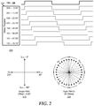
- FIG. 2 illustrates clock waveforms and voltage rail phasing for memory subsystem 100 .
- waveforms 200 illustrates memory clock 108 , and the resulting CLK D signals based upon a three-bit setting field for delay select register 124 , in accordance with a particular example.
- delay select register 124 is loaded with “000,” CLK D is unchanged from memory clock 108 , that is, clock delay module 122 supplies a 0.00° delay.
- An exemplary voltage rail phase diagram 210 illustrates the switching of the high-side MOSFETs for the various voltage rails by a single PMIC when the CLK D is offset by 0.00°, that is, when delay select register 124 is loaded with “000.”
- An exemplary voltage rail phase diagram 220 illustrates the switching of the high-side MOSFETs for the various voltage rails by eight PMICs, each provided with a different one of the eight delayed CLK D signals.
- none of the switching events for any of the eight PMICs are aligned, and thus the peak switching noise injected onto the 12 V power rail is diminished by preventing simultaneous steady-state MOSFET switching, such that the amount of inductance needed to lower the noise in the 12 V power rail is reduced.
- delay select register 124 provides eight selectable delays, but this is not necessarily so, and a greater or a lesser number of selectable delays may be provided by a delay select register, as needed or desired.
- a delay select register may provide 16 selectable delays, each selection incrementally providing delays in steps of 5.625°.
- memory subsystem 100 operates to manage the delays provided to the PMICs based upon the number and variety of memory modules that are populated within the memory subsystem. For example, when memory subsystem 100 includes eight memory modules similar to memory module 110 , then, using the example of FIG. 2 , each one of the memory modules can be configured with a different delay select register setting, such that none of the switching times for any of the eight PMICs are aligned. In another example, when memory subsystem 100 includes two memory modules similar to memory module 110 , then, using the example of FIG.
- a first memory module can be configured with a delay select register set to “000” and a second memory module can be configured with a delay select register set to “100.” In this way, the switching events would be separated by 45°.
- Other numbers of memory modules can likewise be configured with delay select registers set to equalize the switching events of the particular number of memory modules.
- system BIOS 150 operates to program the various delay select registers during a system boot process for memory subsystem 100 .
- a memory reference code portion of system BIOS 150 can determine a number of installed memory modules and program the delay select registers based upon the number of installed memory modules.
- BMC 104 operates to program the various delay select registers out-of-band from the normal processing for memory subsystem 100 .
- BMC 104 can determine a number of installed memory modules and to program the delay select registers based upon the number of installed memory modules.
- memory modules may instantiate a default delay.
- one or more pins of a connector can be allocated to provide a slot ID associated with a location of the memory module within the system architecture. Then, based upon the slot location of each particular memory module, and the associated slot ID, the default delay can be provided in delay select register 124 . Then further, the default delay can be over-written as described above.
- FIG. 3 illustrates a memory subsystem 300 of an information handling system, including a memory clock (CLK) 302 and memory domains 410 , 420 , 430 , and 440 .
- Memory domain 310 includes a memory controller 314 and memory modules 316 and 318 .
- Memory domain 320 includes a memory controller 324 and memory modules 326 and 328 .
- Memory domain 330 includes a memory controller 334 and memory modules 336 and 338 .
- Memory domain 340 includes a memory controller 344 and memory modules 346 and 348 .
- each of memory modules 316 , 318 , 326 , 328 , 336 , 338 , 346 , and 348 are identified by a particular slot ID, for example, based upon one or more pins of a connector, as described above.
- each of memory modules 316 , 318 , 326 , 328 , 336 , 338 , 346 , and 348 includes an associated delay module 317 , 319 , 327 , 329 , 337 , 339 , 347 , and 349 , and each of the delay modules operate to select a delay for the associated memory module.
- FIG. 4 illustrates a memory subsystem 400 of an information handling system, including a memory controller 402 , a baseboard management controller 404 , and one or more memory module 410 .
- Memory subsystem 400 also includes a memory clock (CLK) 406 that is provided to memory controller 402 and a memory clock (MCLK) 407 that is provided from the memory controller to memory module 410 , and a power rail (12V) 408 that is provided to the memory module.
- Memory controller 402 is similar to memory controller 102
- BMC 404 is similar to BMC 104 .
- Memory module 410 is similar to memory module 110 , and includes a RCD 420 , a SPD hub 430 , and PMICs 440 , 442 , 444 , and 446 .
- RCD 420 includes clock delay modules 422 , 424 , 426 , and 428 , and delay select registers 429 .
- PMICs 440 , 442 , 444 , and 446 are typically provided as separate PMICs on a common memory module 410 .
- each memory type may require its own specific voltage.
- a memory module may include various mixes of DRAM, Flash, Phase-Change Memory (PCM), Magnetoresistive-RAM (MRAM), Nano-RAM (NRAM), or the like, various types of devices, such as memory devices, Application Specific Integrated Circuits (ASICs), Field-Programmable Gate Arrays (FPGAs), or the like, or other combinations, as needed or desired.
- the problems associated with switching transient noise being injected onto power rail 408 may remain an issue to be resolved, with the added problem that the switching transient noise may be a bigger issue on memory module 410 because, if the high-side switching aligns between PMICs 440 , 442 , 444 , and 446 , the more localized nature of the noise means that smaller noise spikes that are local to the memory module may cause signal quality problems on the memory module that may not be experienced on other memory modules of memory subsystem 100 .
- memory clock 407 is provided to memory controller 402 and to RCD 420 , where the memory clock is distributed unmodified to the memory storage devices of memory module 410 , and the elements of the memory subsystem that are required to be within a common clock domain share the unmodified memory clock.
- memory clock 407 is provided to clock delay modules 422 , 424 , 426 , and 428 which each operate to provide a selectable delay to the memory clock and to supply the delayed clock (CLK D1 -CLK D4 ) to PMICs 440 , 442 , 444 , and 446 to clock the switching regulators of the PMICs.
- Clock delay modules 422 , 424 , 426 , and 428 provide the selectable delay to memory clock 404 based upon the contents of delay select registers 429 .
- Delay select registers 429 being resident with RCD 420 , is accessible to memory controller 402 via control memory transactions on the memory channel between the RCD, such that the contents of the delay select register may be loaded by a system BIOS during a system boot process for memory subsystem 400 , or during run time operations of the memory subsystem. Further, delay select register 429 is accessible to SPD hub 430 , such that the contents of the delay select register may be loaded during a side-band operation performed by BMC 404 .
- providing the delayed clocks (CLK D1 -CLK D4 ) inputs to PMICs 440 , 442 , 444 , and 446 ensures that the switching events on all of the PMICs are slewed to evenly distribute the noise events on memory module 410 .
- memory subsystem 400 operates to manage the delays provided to the PMICs based upon the number and variety of memory modules that are populated within the memory subsystem.
- memory subsystem 400 operates to consider memory modules with multiple PMICs, and to program the delays for each PMIC intelligently, as described above.
- Such programming can be performed by a system BIOS or a BMC, as described above.
- the delays provided by delay modules similar to delay modules 422 , 424 , 426 , and 428 are not selectable, but are fixed, and a not selectable.
- the RCD may not include delay select registers, and the received memory clock is delayed to provide delayed clocks (CLK D1 -CLK D2 ) based upon the fixed delays.
- memory modules that are installed into a memory subsystem that does not intelligently manage the delays to the PMICs of the memory modules installed into the memory subsystem may still benefit from the slewed switching transients on the memory module.
- FIG. 5 illustrates a memory subsystem 500 of an information handling system, including a memory clock (CLK) 502 and memory domains 510 , 520 , 530 , 540 , 550 , 560 , 570 , and 580 .
- Memory domain 510 includes a clock delay module 512 , a memory controller 514 , and memory modules 516 and 518 .
- Memory domain 520 includes a clock delay module 522 , a memory controller 524 , and memory modules 526 and 528 .
- Memory domain 530 includes a clock delay module 532 , a memory controller 534 , and memory modules 536 and 538 .
- Memory domain 540 includes a clock delay module 542 , a memory controller 544 , and memory modules 546 and 548 .
- Memory domain 550 includes a clock delay module 552 , a memory controller 554 , and memory modules 556 and 558 .
- Memory domain 560 includes a clock delay module 562 , a memory controller 564 , and memory modules 566 and 568 .
- Memory domain 570 includes a clock delay module 572 , a memory controller 574 , and memory modules 576 and 578 .
- Memory domain 580 includes a clock delay module 582 , a memory controller 584 , and memory modules 586 and 588 .
- Clock delay modules 512 , 522 , 532 , 542 , 552 , 562 , 572 , and 582 each receive memory clock 502 and provide a respective delayed clock signal (CLK D1 -CLK D8 ) output to the respective memory modules 514 , 524 , 534 , 544 , 554 , 564 , 574 , and 584 , and to respective memory modules 516 , 518 , 526 , 528 , 536 , 538 , 546 , 548 , 556 , 558 , 566 , 568 , 576 , 578 , 586 , and 588 .
- each of clock delay modules 512 , 522 , 532 , 542 , 552 , 562 , 572 , and 582 is provided to distribute the switching transients from the PMICs of memory modules 516 , 518 , 526 , 528 , 536 , 538 , 546 , 548 , 556 , 558 , 566 , 568 , 576 , 578 , 586 , and 588 , as described above.
- the delays provided by clock delay modules 512 , 522 , 532 , 542 , 552 , 562 , 572 , and 582 may be selectable, as described above, or may be predetermined and fixed based upon the particular design of memory subsystem 500 , as described above. In this way, a memory subsystem that includes memory modules that do not allow for the intelligent management of the delays to the PMICs of the memory modules may still benefit from slewed switching transients on the memory modules.
- FIG. 6 illustrates a method for power plane noise reduction in a memory module starting at block 602 .
- a memory clock is received in block 604 and a clock delay setting is received in block 606 .
- a memory module similar to memory modules 110 or 310 can receive a memory clock and can receive one or more clock delay settings for the PMICs on the memory module.
- a group of delay modules one each for a different memory domain, as depicted in FIG. 5 , can each receive a memory clock, each delay module providing either a pre-set delay or a programmed delay, as needed or desired.
- the memory clock is delayed based upon the clock delay setting in block 608 and the method ends in block 610 .
- the delay module can provide the delay in accordance with the associated clock delay register, and can provide the delayed clock to the one or more PMICs on the memory module.
- the delay modules associated with each memory domain on a memory subsystem similar to memory subsystem 400 can provide the delayed memory clock to the elements of the associated memory domain, such as the memory controller and the memory modules of the memory domain.
- FIG. 7 illustrates a method for power plane noise reduction in a memory subsystem of an information handling system starting at block 702 .
- a memory configuration is determined in block 704 .
- the memory configuration can be determined by a system BIOS during a system boot process for an information handling system, or a BMC can determine the memory configuration during an out-of-band process.
- the clock delays for the memory modules or memory domains for the determined memory configuration are set to slew the noise spikes created by switching the high-side MOSFETs of the PMICs of the memory subsystem in block 704 , and the method ends in block 706 .
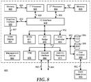
- FIG. 8 illustrates a generalized embodiment of an information handling system 800 similar to information handling system 100 .
- an information handling system can include any instrumentality or aggregate of instrumentalities operable to compute, classify, process, transmit, receive, retrieve, originate, switch, store, display, manifest, detect, record, reproduce, handle, or utilize any form of information, intelligence, or data for business, scientific, control, entertainment, or other purposes.
- information handling system 800 can be a personal computer, a laptop computer, a smart phone, a tablet device or other consumer electronic device, a network server, a network storage device, a switch router or other network communication device, or any other suitable device and may vary in size, shape, performance, functionality, and price.
- information handling system 800 can include processing resources for executing machine-executable code, such as a central processing unit (CPU), a programmable logic array (PLA), an embedded device such as a System-on-a-Chip (SoC), or other control logic hardware.
- Information handling system 800 can also include one or more computer-readable medium for storing machine-executable code, such as software or data.
- Additional components of information handling system 800 can include one or more storage devices that can store machine-executable code, one or more communications ports for communicating with external devices, and various input and output (I/O) devices, such as a keyboard, a mouse, and a video display.
- Information handling system 800 can also include one or more buses operable to transmit information between the various hardware components.
- Information handling system 800 can include devices or modules that embody one or more of the devices or modules described below, and operates to perform one or more of the methods described below.
- Information handling system 800 includes a processors 802 and 804 , an input/output (I/O) interface 810 , memories 820 and 825 , a graphics interface 830 , a basic input and output system/universal extensible firmware interface (BIOS/UEFI) module 840 , a disk controller 850 , a hard disk drive (HDD) 854 , an optical disk drive (ODD) 856 , a disk emulator 860 connected to an external solid state drive (SSD) 862 , an I/O bridge 870 , one or more add-on resources 874 , a trusted platform module (TPM) 876 , a network interface 880 , a management device 890 , and a power supply 895 .
- I/O input/output
- BIOS/UEFI basic input and output system/universal extensible firmware interface
- Processors 802 and 804 , I/O interface 810 , memory 820 , graphics interface 830 , BIOS/UEFI module 840 , disk controller 850 , HDD 854 , ODD 856 , disk emulator 860 , SSD 862 , I/O bridge 870 , add-on resources 874 , TPM 876 , and network interface 880 operate together to provide a host environment of information handling system 800 that operates to provide the data processing functionality of the information handling system.
- the host environment operates to execute machine-executable code, including platform BIOS/UEFI code, device firmware, operating system code, applications, programs, and the like, to perform the data processing tasks associated with information handling system 800 .
- processor 802 is connected to I/O interface 810 via processor interface 806
- processor 804 is connected to the I/O interface via processor interface 808
- Memory 820 is connected to processor 802 via a memory interface 822
- Memory 825 is connected to processor 804 via a memory interface 827
- Graphics interface 830 is connected to I/O interface 810 via a graphics interface 832 , and provides a video display output 836 to a video display 834 .
- information handling system 800 includes separate memories that are dedicated to each of processors 802 and 804 via separate memory interfaces.
- An example of memories 820 and 830 include random access memory (RAM) such as static RAM (SRAM), dynamic RAM (DRAM), non-volatile RAM (NV-RAM), or the like, read only memory (ROM), another type of memory, or a combination thereof.
- RAM random access memory
- SRAM static RAM
- DRAM dynamic RAM
- NV-RAM non-volatile RAM
- ROM read only memory
- BIOS/UEFI module 840 , disk controller 850 , and I/O bridge 870 are connected to I/O interface 810 via an I/O channel 812 .
- I/O channel 812 includes a Peripheral Component Interconnect (PCI) interface, a PCI-Extended (PCI-X) interface, a high speed PCI-Express (PCIe) interface, another industry standard or proprietary communication interface, or a combination thereof.
- PCI Peripheral Component Interconnect
- PCI-X PCI-Extended
- PCIe high speed PCI-Express
- I/O interface 810 can also include one or more other I/O interfaces, including an Industry Standard Architecture (ISA) interface, a Small Computer Serial Interface (SCSI) interface, an Inter-Integrated Circuit (I 2 C) interface, a System Packet Interface (SPI), a Universal Serial Bus (USB), another interface, or a combination thereof.
- BIOS/UEFI module 840 includes BIOS/UEFI code operable to detect resources within information handling system 800 , to provide drivers for the resources, initialize the resources, and access the resources.
- BIOS/UEFI module 840 includes code that operates to detect resources within information handling system 800 , to provide drivers for the resources, to initialize the resources, and to access the resources.
- Disk controller 850 includes a disk interface 852 that connects the disk controller to HDD 854 , to ODD 856 , and to disk emulator 860 .
- An example of disk interface 852 includes an Integrated Drive Electronics (IDE) interface, an Advanced Technology Attachment (ATA) such as a parallel ATA (PATA) interface or a serial ATA (SATA) interface, a SCSI interface, a USB interface, a proprietary interface, or a combination thereof.
- Disk emulator 860 permits SSD 864 to be connected to information handling system 800 via an external interface 862 .
- An example of external interface 862 includes a USB interface, an IEEE 1394 (Firewire) interface, a proprietary interface, or a combination thereof.
- solid-state drive 864 can be disposed within information handling system 800 .
- I/O bridge 870 includes a peripheral interface 872 that connects the I/O bridge to add-on resource 874 , to TPM 876 , and to network interface 880 .
- Peripheral interface 872 can be the same type of interface as I/O channel 812 , or can be a different type of interface.
- I/O bridge 870 extends the capacity of I/O channel 812 when peripheral interface 872 and the I/O channel are of the same type, and the I/O bridge translates information from a format suitable to the I/O channel to a format suitable to the peripheral channel 872 when they are of a different type.
- Add-on resource 874 can include a data storage system, an additional graphics interface, a network interface card (NIC), a sound/video processing card, another add-on resource, or a combination thereof.
- Add-on resource 874 can be on a main circuit board, on separate circuit board or add-in card disposed within information handling system 800 , a device that is external to the information handling system, or a combination thereof.
- Network interface 880 represents a NIC disposed within information handling system 800 , on a main circuit board of the information handling system, integrated onto another component such as I/O interface 810 , in another suitable location, or a combination thereof.
- Network interface device 880 includes network channels 882 and 884 that provide interfaces to devices that are external to information handling system 800 .
- network channels 882 and 884 are of a different type than peripheral channel 872 and network interface 880 translates information from a format suitable to the peripheral channel to a format suitable to external devices.
- An example of network channels 882 and 884 includes InfiniBand channels, Fibre Channel channels, Gigabit Ethernet channels, proprietary channel architectures, or a combination thereof.
- Network channels 882 and 884 can be connected to external network resources (not illustrated).
- the network resource can include another information handling system, a data storage system, another network, a grid management system, another suitable resource, or a combination thereof.
- Management device 890 represents one or more processing devices, such as a dedicated baseboard management controller (BMC) System-on-a-Chip (SoC) device, one or more associated memory devices, one or more network interface devices, a complex programmable logic device (CPLD), and the like, that operate together to provide the management environment for information handling system 800 .
- BMC dedicated baseboard management controller
- SoC System-on-a-Chip
- CPLD complex programmable logic device
- management device 890 is connected to various components of the host environment via various internal communication interfaces, such as a Low Pin Count (LPC) interface, an Inter-Integrated-Circuit (I2C) interface, a PCIe interface, or the like, to provide an out-of-band (OOB) mechanism to retrieve information related to the operation of the host environment, to provide BIOS/UEFI or system firmware updates, to manage non-processing components of information handling system 800 , such as system cooling fans and power supplies.
- Management device 890 can include a network connection to an external management system, and the management device can communicate with the management system to report status information for information handling system 800 , to receive BIOS/UEFI or system firmware updates, or to perform other task for managing and controlling the operation of information handling system 800 .
- Management device 890 can operate off of a separate power plane from the components of the host environment so that the management device receives power to manage information handling system 800 when the information handling system is otherwise shut down.
- An example of management device 890 include a commercially available BMC product or other device that operates in accordance with an Intelligent Platform Management Initiative (IPMI) specification, a Web Services Management (WSMan) interface, a Redfish Application Programming Interface (API), another Distributed Management Task Force (DMTF), or other management standard, and can include an Integrated Dell Remote Access Controller (iDRAC), an Embedded Controller (EC), or the like.
- IPMI Intelligent Platform Management Initiative
- WSMan Web Services Management
- API Redfish Application Programming Interface
- DMTF Distributed Management Task Force
- Management device 890 may further include associated memory devices, logic devices, security devices, or the like, as needed or desired.
Landscapes
- Engineering & Computer Science (AREA)
- Theoretical Computer Science (AREA)
- Power Engineering (AREA)
- Physics & Mathematics (AREA)
- General Engineering & Computer Science (AREA)
- General Physics & Mathematics (AREA)
- Microelectronics & Electronic Packaging (AREA)
- Computer Hardware Design (AREA)
- Memory System (AREA)
- Power Sources (AREA)
Abstract
Description
Claims (18)
Priority Applications (1)
| Application Number | Priority Date | Filing Date | Title |
|---|---|---|---|
| US16/815,191 US11222687B2 (en) | 2020-03-11 | 2020-03-11 | System and method for power plane noise reduction in a memory subsystem of an information handling system |
Applications Claiming Priority (1)
| Application Number | Priority Date | Filing Date | Title |
|---|---|---|---|
| US16/815,191 US11222687B2 (en) | 2020-03-11 | 2020-03-11 | System and method for power plane noise reduction in a memory subsystem of an information handling system |
Publications (2)
| Publication Number | Publication Date |
|---|---|
| US20210287730A1 US20210287730A1 (en) | 2021-09-16 |
| US11222687B2 true US11222687B2 (en) | 2022-01-11 |
Family
ID=77664933
Family Applications (1)
| Application Number | Title | Priority Date | Filing Date |
|---|---|---|---|
| US16/815,191 Active US11222687B2 (en) | 2020-03-11 | 2020-03-11 | System and method for power plane noise reduction in a memory subsystem of an information handling system |
Country Status (1)
| Country | Link |
|---|---|
| US (1) | US11222687B2 (en) |
Families Citing this family (4)
| Publication number | Priority date | Publication date | Assignee | Title |
|---|---|---|---|---|
| CN113760181B (en) | 2020-06-05 | 2024-10-01 | 美光科技公司 | Method for tuning command/address bus timing and memory device and memory system using the same |
| US11948661B2 (en) * | 2020-06-05 | 2024-04-02 | Micron Technology, Inc. | Methods for tuning command/address bus timing and memory devices and memory systems using the same |
| US11797229B2 (en) * | 2020-07-02 | 2023-10-24 | Micron Technology, Inc. | Multiple register clock driver loaded memory subsystem |
| US20210183410A1 (en) * | 2020-12-23 | 2021-06-17 | Intel Corporation | Improved memory module that conserves motherboard wiring space |
Citations (7)
| Publication number | Priority date | Publication date | Assignee | Title |
|---|---|---|---|---|
| US20140304445A1 (en) * | 2013-04-09 | 2014-10-09 | William Michael Gervasi | Memory bus loading and conditioning module |
| US9405355B2 (en) | 2012-08-21 | 2016-08-02 | Micron Technology, Inc. | Memory operation power management by data transfer time adjustment |
| US9584014B2 (en) * | 2013-11-15 | 2017-02-28 | Kabushiki Kaisha Toshiba | DC-DC converter |
| US20190123646A1 (en) * | 2017-10-23 | 2019-04-25 | Dialog Semiconductor (Uk) Limited | Boost Spread-Spectrum Technique in Pulse Skip Mode with Fixed Frequency Clock Reference |
| US20190340141A1 (en) * | 2018-05-01 | 2019-11-07 | Integrated Device Technology, Inc. | Ddr5 rcd interface protocol and operation |
| US20200118612A1 (en) * | 2018-10-10 | 2020-04-16 | Integrated Device Technology, Inc. | Monotonic variable delay line |
| US20210141747A1 (en) * | 2019-11-12 | 2021-05-13 | Samsung Electronics Co., Ltd. | Memory device performing self-calibration by identifying location information and memory module including the same |
-
2020
- 2020-03-11 US US16/815,191 patent/US11222687B2/en active Active
Patent Citations (7)
| Publication number | Priority date | Publication date | Assignee | Title |
|---|---|---|---|---|
| US9405355B2 (en) | 2012-08-21 | 2016-08-02 | Micron Technology, Inc. | Memory operation power management by data transfer time adjustment |
| US20140304445A1 (en) * | 2013-04-09 | 2014-10-09 | William Michael Gervasi | Memory bus loading and conditioning module |
| US9584014B2 (en) * | 2013-11-15 | 2017-02-28 | Kabushiki Kaisha Toshiba | DC-DC converter |
| US20190123646A1 (en) * | 2017-10-23 | 2019-04-25 | Dialog Semiconductor (Uk) Limited | Boost Spread-Spectrum Technique in Pulse Skip Mode with Fixed Frequency Clock Reference |
| US20190340141A1 (en) * | 2018-05-01 | 2019-11-07 | Integrated Device Technology, Inc. | Ddr5 rcd interface protocol and operation |
| US20200118612A1 (en) * | 2018-10-10 | 2020-04-16 | Integrated Device Technology, Inc. | Monotonic variable delay line |
| US20210141747A1 (en) * | 2019-11-12 | 2021-05-13 | Samsung Electronics Co., Ltd. | Memory device performing self-calibration by identifying location information and memory module including the same |
Also Published As
| Publication number | Publication date |
|---|---|
| US20210287730A1 (en) | 2021-09-16 |
Similar Documents
| Publication | Publication Date | Title |
|---|---|---|
| US11222687B2 (en) | System and method for power plane noise reduction in a memory subsystem of an information handling system | |
| US8402208B2 (en) | Configurable memory controller/memory module communication system | |
| US20180246643A1 (en) | System and Method to Perform Runtime Saves on Dual Data Rate NVDIMMs | |
| US10331593B2 (en) | System and method for arbitration and recovery of SPD interfaces in an information handling system | |
| US9921629B2 (en) | Systems and methods for a multi-rail voltage regulator with configurable phase allocation | |
| US20110138162A1 (en) | Reconfigurable load-reduced memory buffer | |
| US11093419B2 (en) | System and method for cost and power optimized heterogeneous dual-channel DDR DIMMs | |
| US11341037B2 (en) | System and method for providing per channel frequency optimization in a double data rate memory system | |
| US10877918B2 (en) | System and method for I/O aware processor configuration | |
| US20230387799A1 (en) | Method for providing dynamic voltage regulator characteristic changes | |
| US12230360B2 (en) | Controlling memory module clock buffer power in a system with dual memory clocks per memory module | |
| US12001332B2 (en) | Runtime de-interleave and re-interleave of system memory | |
| US20230046702A1 (en) | Temperature based decision feedback equalization retraining | |
| US12147684B2 (en) | Method for power reduction in memory modules | |
| US20180004274A1 (en) | Determining power state support | |
| US12334187B2 (en) | Power reduction in a clock buffer of a memory module based upon memory module topology | |
| US12315594B2 (en) | Controlling memory module clock buffer power in a system with a single memory clock per memory module | |
| US12334188B2 (en) | Power reduction in a clock buffer of a memory module based upon memory module speed | |
| US12541479B2 (en) | Single-port and dual-port EDSFF media port control | |
| US11960899B2 (en) | Dual in-line memory module map-out in an information handling system | |
| US12292823B2 (en) | CPLD as adapter for high-availability drive management | |
| US12135596B2 (en) | Fast bleed of power rails | |
| US12487950B2 (en) | System power reduction for DDR5 information handling systems | |
| US12001851B2 (en) | Power conservation and standby graphics rendering in an information handling system | |
| US11468169B1 (en) | Dark storage support for as-a-service model |
Legal Events
| Date | Code | Title | Description |
|---|---|---|---|
| AS | Assignment |
Owner name: DELL PRODUCTS, LP, TEXAS Free format text: ASSIGNMENT OF ASSIGNORS INTEREST;ASSIGNORS:BERKE, STUART A.;CHIN, JORDAN;JOHNSON, RALPH H.;AND OTHERS;SIGNING DATES FROM 20200302 TO 20200309;REEL/FRAME:052080/0640 |
|
| FEPP | Fee payment procedure |
Free format text: ENTITY STATUS SET TO UNDISCOUNTED (ORIGINAL EVENT CODE: BIG.); ENTITY STATUS OF PATENT OWNER: LARGE ENTITY |
|
| AS | Assignment |
Owner name: THE BANK OF NEW YORK MELLON TRUST COMPANY, N.A., TEXAS Free format text: SECURITY AGREEMENT;ASSIGNORS:CREDANT TECHNOLOGIES INC.;DELL INTERNATIONAL L.L.C.;DELL MARKETING L.P.;AND OTHERS;REEL/FRAME:053546/0001 Effective date: 20200409 |
|
| AS | Assignment |
Owner name: CREDIT SUISSE AG, CAYMAN ISLANDS BRANCH, NORTH CAROLINA Free format text: SECURITY AGREEMENT;ASSIGNORS:DELL PRODUCTS L.P.;EMC IP HOLDING COMPANY LLC;REEL/FRAME:052771/0906 Effective date: 20200528 |
|
| AS | Assignment |
Owner name: THE BANK OF NEW YORK MELLON TRUST COMPANY, N.A., AS COLLATERAL AGENT, TEXAS Free format text: SECURITY INTEREST;ASSIGNORS:DELL PRODUCTS L.P.;EMC CORPORATION;EMC IP HOLDING COMPANY LLC;REEL/FRAME:053311/0169 Effective date: 20200603 Owner name: THE BANK OF NEW YORK MELLON TRUST COMPANY, N.A., AS COLLATERAL AGENT, TEXAS Free format text: SECURITY INTEREST;ASSIGNORS:DELL PRODUCTS L.P.;EMC IP HOLDING COMPANY LLC;REEL/FRAME:052852/0022 Effective date: 20200603 Owner name: THE BANK OF NEW YORK MELLON TRUST COMPANY, N.A., AS COLLATERAL AGENT, TEXAS Free format text: SECURITY INTEREST;ASSIGNORS:DELL PRODUCTS L.P.;EMC IP HOLDING COMPANY LLC;REEL/FRAME:052851/0917 Effective date: 20200603 Owner name: THE BANK OF NEW YORK MELLON TRUST COMPANY, N.A., AS COLLATERAL AGENT, TEXAS Free format text: SECURITY INTEREST;ASSIGNORS:DELL PRODUCTS L.P.;EMC IP HOLDING COMPANY LLC;THE BANK OF NEW YORK MELLON TRUST COMPANY, N.A., AS COLLATERAL AGENT;REEL/FRAME:052851/0081 Effective date: 20200603 |
|
| STPP | Information on status: patent application and granting procedure in general |
Free format text: NOTICE OF ALLOWANCE MAILED -- APPLICATION RECEIVED IN OFFICE OF PUBLICATIONS |
|
| AS | Assignment |
Owner name: EMC IP HOLDING COMPANY LLC, TEXAS Free format text: RELEASE OF SECURITY INTEREST AT REEL 052771 FRAME 0906;ASSIGNOR:CREDIT SUISSE AG, CAYMAN ISLANDS BRANCH;REEL/FRAME:058001/0298 Effective date: 20211101 Owner name: DELL PRODUCTS L.P., TEXAS Free format text: RELEASE OF SECURITY INTEREST AT REEL 052771 FRAME 0906;ASSIGNOR:CREDIT SUISSE AG, CAYMAN ISLANDS BRANCH;REEL/FRAME:058001/0298 Effective date: 20211101 |
|
| STPP | Information on status: patent application and granting procedure in general |
Free format text: PUBLICATIONS -- ISSUE FEE PAYMENT VERIFIED |
|
| STCF | Information on status: patent grant |
Free format text: PATENTED CASE |
|
| AS | Assignment |
Owner name: EMC IP HOLDING COMPANY LLC, TEXAS Free format text: RELEASE OF SECURITY INTEREST IN PATENTS PREVIOUSLY RECORDED AT REEL/FRAME (052851/0917);ASSIGNOR:THE BANK OF NEW YORK MELLON TRUST COMPANY, N.A., AS NOTES COLLATERAL AGENT;REEL/FRAME:060436/0509 Effective date: 20220329 Owner name: DELL PRODUCTS L.P., TEXAS Free format text: RELEASE OF SECURITY INTEREST IN PATENTS PREVIOUSLY RECORDED AT REEL/FRAME (052851/0917);ASSIGNOR:THE BANK OF NEW YORK MELLON TRUST COMPANY, N.A., AS NOTES COLLATERAL AGENT;REEL/FRAME:060436/0509 Effective date: 20220329 Owner name: EMC IP HOLDING COMPANY LLC, TEXAS Free format text: RELEASE OF SECURITY INTEREST IN PATENTS PREVIOUSLY RECORDED AT REEL/FRAME (052851/0081);ASSIGNOR:THE BANK OF NEW YORK MELLON TRUST COMPANY, N.A., AS NOTES COLLATERAL AGENT;REEL/FRAME:060436/0441 Effective date: 20220329 Owner name: DELL PRODUCTS L.P., TEXAS Free format text: RELEASE OF SECURITY INTEREST IN PATENTS PREVIOUSLY RECORDED AT REEL/FRAME (052851/0081);ASSIGNOR:THE BANK OF NEW YORK MELLON TRUST COMPANY, N.A., AS NOTES COLLATERAL AGENT;REEL/FRAME:060436/0441 Effective date: 20220329 Owner name: EMC IP HOLDING COMPANY LLC, TEXAS Free format text: RELEASE OF SECURITY INTEREST IN PATENTS PREVIOUSLY RECORDED AT REEL/FRAME (053311/0169);ASSIGNOR:THE BANK OF NEW YORK MELLON TRUST COMPANY, N.A., AS NOTES COLLATERAL AGENT;REEL/FRAME:060438/0742 Effective date: 20220329 Owner name: EMC CORPORATION, MASSACHUSETTS Free format text: RELEASE OF SECURITY INTEREST IN PATENTS PREVIOUSLY RECORDED AT REEL/FRAME (053311/0169);ASSIGNOR:THE BANK OF NEW YORK MELLON TRUST COMPANY, N.A., AS NOTES COLLATERAL AGENT;REEL/FRAME:060438/0742 Effective date: 20220329 Owner name: DELL PRODUCTS L.P., TEXAS Free format text: RELEASE OF SECURITY INTEREST IN PATENTS PREVIOUSLY RECORDED AT REEL/FRAME (053311/0169);ASSIGNOR:THE BANK OF NEW YORK MELLON TRUST COMPANY, N.A., AS NOTES COLLATERAL AGENT;REEL/FRAME:060438/0742 Effective date: 20220329 Owner name: EMC IP HOLDING COMPANY LLC, TEXAS Free format text: RELEASE OF SECURITY INTEREST IN PATENTS PREVIOUSLY RECORDED AT REEL/FRAME (052852/0022);ASSIGNOR:THE BANK OF NEW YORK MELLON TRUST COMPANY, N.A., AS NOTES COLLATERAL AGENT;REEL/FRAME:060436/0582 Effective date: 20220329 Owner name: DELL PRODUCTS L.P., TEXAS Free format text: RELEASE OF SECURITY INTEREST IN PATENTS PREVIOUSLY RECORDED AT REEL/FRAME (052852/0022);ASSIGNOR:THE BANK OF NEW YORK MELLON TRUST COMPANY, N.A., AS NOTES COLLATERAL AGENT;REEL/FRAME:060436/0582 Effective date: 20220329 Owner name: DELL MARKETING L.P. (ON BEHALF OF ITSELF AND AS SUCCESSOR-IN-INTEREST TO CREDANT TECHNOLOGIES, INC.), TEXAS Free format text: RELEASE OF SECURITY INTEREST IN PATENTS PREVIOUSLY RECORDED AT REEL/FRAME (053546/0001);ASSIGNOR:THE BANK OF NEW YORK MELLON TRUST COMPANY, N.A., AS NOTES COLLATERAL AGENT;REEL/FRAME:071642/0001 Effective date: 20220329 Owner name: DELL INTERNATIONAL L.L.C., TEXAS Free format text: RELEASE OF SECURITY INTEREST IN PATENTS PREVIOUSLY RECORDED AT REEL/FRAME (053546/0001);ASSIGNOR:THE BANK OF NEW YORK MELLON TRUST COMPANY, N.A., AS NOTES COLLATERAL AGENT;REEL/FRAME:071642/0001 Effective date: 20220329 Owner name: DELL PRODUCTS L.P., TEXAS Free format text: RELEASE OF SECURITY INTEREST IN PATENTS PREVIOUSLY RECORDED AT REEL/FRAME (053546/0001);ASSIGNOR:THE BANK OF NEW YORK MELLON TRUST COMPANY, N.A., AS NOTES COLLATERAL AGENT;REEL/FRAME:071642/0001 Effective date: 20220329 Owner name: DELL USA L.P., TEXAS Free format text: RELEASE OF SECURITY INTEREST IN PATENTS PREVIOUSLY RECORDED AT REEL/FRAME (053546/0001);ASSIGNOR:THE BANK OF NEW YORK MELLON TRUST COMPANY, N.A., AS NOTES COLLATERAL AGENT;REEL/FRAME:071642/0001 Effective date: 20220329 Owner name: EMC CORPORATION, MASSACHUSETTS Free format text: RELEASE OF SECURITY INTEREST IN PATENTS PREVIOUSLY RECORDED AT REEL/FRAME (053546/0001);ASSIGNOR:THE BANK OF NEW YORK MELLON TRUST COMPANY, N.A., AS NOTES COLLATERAL AGENT;REEL/FRAME:071642/0001 Effective date: 20220329 Owner name: DELL MARKETING CORPORATION (SUCCESSOR-IN-INTEREST TO FORCE10 NETWORKS, INC. AND WYSE TECHNOLOGY L.L.C.), TEXAS Free format text: RELEASE OF SECURITY INTEREST IN PATENTS PREVIOUSLY RECORDED AT REEL/FRAME (053546/0001);ASSIGNOR:THE BANK OF NEW YORK MELLON TRUST COMPANY, N.A., AS NOTES COLLATERAL AGENT;REEL/FRAME:071642/0001 Effective date: 20220329 Owner name: EMC IP HOLDING COMPANY LLC, TEXAS Free format text: RELEASE OF SECURITY INTEREST IN PATENTS PREVIOUSLY RECORDED AT REEL/FRAME (053546/0001);ASSIGNOR:THE BANK OF NEW YORK MELLON TRUST COMPANY, N.A., AS NOTES COLLATERAL AGENT;REEL/FRAME:071642/0001 Effective date: 20220329 |
|
| MAFP | Maintenance fee payment |
Free format text: PAYMENT OF MAINTENANCE FEE, 4TH YEAR, LARGE ENTITY (ORIGINAL EVENT CODE: M1551); ENTITY STATUS OF PATENT OWNER: LARGE ENTITY Year of fee payment: 4 |