US11221694B2 - Organic light emitting display apparatus and method of manufacturing the same - Google Patents
Organic light emitting display apparatus and method of manufacturing the same Download PDFInfo
- Publication number
- US11221694B2 US11221694B2 US16/906,884 US202016906884A US11221694B2 US 11221694 B2 US11221694 B2 US 11221694B2 US 202016906884 A US202016906884 A US 202016906884A US 11221694 B2 US11221694 B2 US 11221694B2
- Authority
- US
- United States
- Prior art keywords
- emission region
- layer
- black matrix
- dielectric constant
- emission
- Prior art date
- Legal status (The legal status is an assumption and is not a legal conclusion. Google has not performed a legal analysis and makes no representation as to the accuracy of the status listed.)
- Active, expires
Links
Images


Classifications
-
- G—PHYSICS
- G06—COMPUTING OR CALCULATING; COUNTING
- G06F—ELECTRIC DIGITAL DATA PROCESSING
- G06F3/00—Input arrangements for transferring data to be processed into a form capable of being handled by the computer; Output arrangements for transferring data from processing unit to output unit, e.g. interface arrangements
- G06F3/01—Input arrangements or combined input and output arrangements for interaction between user and computer
- G06F3/03—Arrangements for converting the position or the displacement of a member into a coded form
- G06F3/041—Digitisers, e.g. for touch screens or touch pads, characterised by the transducing means
- G06F3/0412—Digitisers structurally integrated in a display
-
- H—ELECTRICITY
- H10—SEMICONDUCTOR DEVICES; ELECTRIC SOLID-STATE DEVICES NOT OTHERWISE PROVIDED FOR
- H10K—ORGANIC ELECTRIC SOLID-STATE DEVICES
- H10K59/00—Integrated devices, or assemblies of multiple devices, comprising at least one organic light-emitting element covered by group H10K50/00
- H10K59/40—OLEDs integrated with touch screens
-
- G—PHYSICS
- G06—COMPUTING OR CALCULATING; COUNTING
- G06F—ELECTRIC DIGITAL DATA PROCESSING
- G06F3/00—Input arrangements for transferring data to be processed into a form capable of being handled by the computer; Output arrangements for transferring data from processing unit to output unit, e.g. interface arrangements
- G06F3/01—Input arrangements or combined input and output arrangements for interaction between user and computer
- G06F3/03—Arrangements for converting the position or the displacement of a member into a coded form
- G06F3/041—Digitisers, e.g. for touch screens or touch pads, characterised by the transducing means
-
- H01L27/323—
-
- H01L51/5284—
-
- H01L51/56—
-
- H—ELECTRICITY
- H10—SEMICONDUCTOR DEVICES; ELECTRIC SOLID-STATE DEVICES NOT OTHERWISE PROVIDED FOR
- H10K—ORGANIC ELECTRIC SOLID-STATE DEVICES
- H10K50/00—Organic light-emitting devices
- H10K50/80—Constructional details
- H10K50/86—Arrangements for improving contrast, e.g. preventing reflection of ambient light
- H10K50/865—Arrangements for improving contrast, e.g. preventing reflection of ambient light comprising light absorbing layers, e.g. light-blocking layers
-
- H—ELECTRICITY
- H10—SEMICONDUCTOR DEVICES; ELECTRIC SOLID-STATE DEVICES NOT OTHERWISE PROVIDED FOR
- H10K—ORGANIC ELECTRIC SOLID-STATE DEVICES
- H10K59/00—Integrated devices, or assemblies of multiple devices, comprising at least one organic light-emitting element covered by group H10K50/00
- H10K59/10—OLED displays
- H10K59/12—Active-matrix OLED [AMOLED] displays
- H10K59/122—Pixel-defining structures or layers, e.g. banks
-
- H—ELECTRICITY
- H10—SEMICONDUCTOR DEVICES; ELECTRIC SOLID-STATE DEVICES NOT OTHERWISE PROVIDED FOR
- H10K—ORGANIC ELECTRIC SOLID-STATE DEVICES
- H10K59/00—Integrated devices, or assemblies of multiple devices, comprising at least one organic light-emitting element covered by group H10K50/00
- H10K59/80—Constructional details
- H10K59/8791—Arrangements for improving contrast, e.g. preventing reflection of ambient light
- H10K59/8792—Arrangements for improving contrast, e.g. preventing reflection of ambient light comprising light absorbing layers, e.g. black layers
-
- H—ELECTRICITY
- H10—SEMICONDUCTOR DEVICES; ELECTRIC SOLID-STATE DEVICES NOT OTHERWISE PROVIDED FOR
- H10K—ORGANIC ELECTRIC SOLID-STATE DEVICES
- H10K71/00—Manufacture or treatment specially adapted for the organic devices covered by this subclass
-
- G—PHYSICS
- G06—COMPUTING OR CALCULATING; COUNTING
- G06F—ELECTRIC DIGITAL DATA PROCESSING
- G06F2203/00—Indexing scheme relating to G06F3/00 - G06F3/048
- G06F2203/041—Indexing scheme relating to G06F3/041 - G06F3/045
- G06F2203/04103—Manufacturing, i.e. details related to manufacturing processes specially suited for touch sensitive devices
-
- H01L27/3246—
-
- H01L27/3283—
-
- H01L51/5253—
-
- H—ELECTRICITY
- H10—SEMICONDUCTOR DEVICES; ELECTRIC SOLID-STATE DEVICES NOT OTHERWISE PROVIDED FOR
- H10K—ORGANIC ELECTRIC SOLID-STATE DEVICES
- H10K50/00—Organic light-emitting devices
- H10K50/80—Constructional details
- H10K50/84—Passivation; Containers; Encapsulations
- H10K50/844—Encapsulations
-
- H—ELECTRICITY
- H10—SEMICONDUCTOR DEVICES; ELECTRIC SOLID-STATE DEVICES NOT OTHERWISE PROVIDED FOR
- H10K—ORGANIC ELECTRIC SOLID-STATE DEVICES
- H10K59/00—Integrated devices, or assemblies of multiple devices, comprising at least one organic light-emitting element covered by group H10K50/00
- H10K59/10—OLED displays
- H10K59/17—Passive-matrix OLED displays
- H10K59/173—Passive-matrix OLED displays comprising banks or shadow masks
Definitions
- aspects of one or more example embodiments relate to an organic light emitting display apparatus and a method of manufacturing the organic light emitting display apparatus.
- an organic light emitting display apparatus may display images based on a principle in which holes and electrons respectively injected from an anode and a cathode recombine in an emission layer to emit light.
- Pixels in a display device have a structure including an electroluminescence (EL) device including an emission layer between a pixel electrode as an anode and an opposite electrode as a cathode.
- EL electroluminescence
- a touch screen layer for sensing touch input from users may be provided on a display layer where the pixels are arranged.
- aspects of one or more example embodiments relate to an organic light emitting display apparatus and a method of manufacturing the organic light emitting display apparatus, and for example, to an organic light emitting display apparatus including an internal touch screen layer and a method of manufacturing the organic light emitting display apparatus.
- a phenomenon may occur in which the sensitivity of a touch electrode in the touch screen layer is not uniformly formed over the entire surface of the touch screen layer and thus causing some regions to be relatively sensitive and some other regions to be relatively insensitive. For example, there may be a large sensitivity difference between a region of a spacer, which is formed in the display layer to seat a mask for depositing the emission layer, and the other regions. Such characteristics may be caused by a large difference in the interval between the touch electrode and the opposite electrode formed thereon due to the spacer protruding higher than the periphery.
- the non-uniformity of touch sensitivity may lead to poor performance of the touch sensor.
- one or more example embodiments include an organic light emitting display apparatus having a relatively improved touch sensitivity difference in each region due to a spacer or the like and a method of manufacturing the organic light emitting display apparatus.
- an organic light emitting display apparatus includes a display layer including an emission region, a first non-emission region in which a pixel definition layer surrounding the emission region is arranged, and a second non-emission region in which a spacer is provided on the pixel definition layer, and a touch screen layer including a touch electrode arranged at a position corresponding to the first non-emission region and the second non-emission region, wherein the touch screen layer further includes a sensitivity compensation layer including a first dielectric constant portion and a second dielectric constant portion of different dielectric constants arranged to respectively correspond to the first non-emission region and the second non-emission region.
- a dielectric constant of the second dielectric constant portion may be greater than a dielectric constant of the first dielectric constant portion.
- the organic light emitting display apparatus may further include, on an opposite side of the touch screen layer with respect to a side facing the display layer, a light blocking layer including a first black matrix and a second black matrix respectively covering the first non-emission region and the second non-emission region.
- the light blocking layer may further include a transparent organic layer covering the emission region, and the transparent organic layer may also cover the first black matrix and the second black matrix.
- the light blocking layer may further include a transparent organic layer covering the emission region, and the transparent organic layer may cover the first black matrix and may not cover the second black matrix.
- the organic light emitting display apparatus may further include, between the display layer and the touch screen layer, a light blocking layer including a first black matrix and a second black matrix respectively covering the first non-emission region and the second non-emission region.
- the light blocking layer may further include a transparent organic layer covering the emission region, and the transparent organic layer may also cover the first black matrix and the second black matrix.
- the light blocking layer may further include a transparent organic layer covering the emission region, and the transparent organic layer may cover the first black matrix and may not cover the second black matrix.
- the display layer may further include an emission layer arranged in the emission region, and a pixel electrode and an opposite electrode arranged to face each other with the emission layer therebetween, and the opposite electrode may be arranged across the emission region, the first non-emission region, and the second non-emission region.
- a method of manufacturing an organic light emitting display apparatus includes forming a display layer including an emission region, a first non-emission region in which a pixel definition layer surrounding the emission region is arranged, and a second non-emission region in which a spacer is provided on the pixel definition layer, and forming, on the display layer, a sensitivity compensation layer including a first dielectric constant portion and a second dielectric constant portion having different dielectric constants and arranged to respectively correspond to the first non-emission region and the second non-emission region, and a touch screen layer including a touch electrode arranged at a position corresponding to the first non-emission region and the second non-emission region.
- a dielectric constant of the second dielectric constant portion may be formed to be greater than a dielectric constant of the first dielectric constant portion.
- the method may further include forming, on an opposite side of the touch screen layer with respect to a side facing the display layer, a light blocking layer including a first black matrix and a second black matrix respectively covering the first non-emission region and the second non-emission region.
- the light blocking layer may further include a transparent organic layer covering the emission region, and the transparent organic layer may be formed to also cover the first black matrix and the second black matrix.
- the light blocking layer may further include a transparent organic layer covering the emission region, and the transparent organic layer may be formed to cover the first black matrix and not to cover the second black matrix.
- the method may further include forming, between the display layer and the touch screen layer, a light blocking layer including a first black matrix and a second black matrix respectively covering the first non-emission region and the second non-emission region.
- the light blocking layer may further include a transparent organic layer covering the emission region, and the transparent organic layer may be formed to also cover the first black matrix and the second black matrix.
- the light blocking layer may further include a transparent organic layer covering the emission region, and the transparent organic layer may be formed to cover the first black matrix and not to cover the second black matrix.
- the display layer may further include an emission layer arranged in the emission region, and a pixel electrode and an opposite electrode arranged to face each other with the emission layer therebetween, and the opposite electrode may be formed to be arranged across the emission region, the first non-emission region, and the second non-emission region.
- FIG. 1 is a cross-sectional view of an organic light emitting display apparatus according to some example embodiments
- FIGS. 2A to 2D are cross-sectional views sequentially illustrating a process of manufacturing the organic light emitting display apparatus illustrated in FIG. 1 ;
- FIG. 3 is a cross-sectional view of an organic light emitting display apparatus according to some example embodiments.
- FIG. 4 is a cross-sectional view of an organic light emitting display apparatus according to some example embodiments.
- FIGS. 5A to 5E are cross-sectional views sequentially illustrating a process of manufacturing the organic light emitting display apparatus illustrated in FIG. 4 ;
- FIG. 6 is a cross-sectional view of an organic light emitting display apparatus according to some example embodiments.
- FIG. 7 is a graph illustrating the correlation between the dielectric constant of a sensitivity compensation layer and the S/N of a touch electrode.
- the expression “at least one of a, b, or c” indicates only a, only b, only c, both a and b, both a and c, both b and c, all of a, b, and c, or variations thereof.
- a particular process order may be performed differently from the described order. For example, two consecutively described processes may be performed substantially at the same time or performed in an order opposite to the described order.
- a layer, region, or component when a layer, region, or component is referred to as being “connected to” another layer, region, or component, it may be “directly connected to” the other layer, region, or component or may be “indirectly connected to” the other layer, region, or component with one or more intervening layers, regions, or components therebetween.
- a layer, region, or component when a layer, region, or component is referred to as being “electrically connected to” another layer, region, or component, it may be “directly electrically connected to” the other layer, region, or component or may be “indirectly electrically connected to” the other layer, region, or component with one or more intervening layers, regions, or components therebetween.
- FIG. 1 is a cross-sectional view of an organic light emitting display apparatus according to some example embodiments.
- EL device is illustrated as a reference; however, it may be considered that a plurality of EL devices are distributed in an actual product.
- the organic light emitting display apparatus may include a display layer 100 in which an image (e.g., a static image or video images) are displayed, a touch screen layer 200 for a touch operation (e.g., for sensing touch input, for example, from a user or an external object such as a stylus), a light blocking layer 300 covering non-emission regions 11 and 12 other than an emission region 10 by black matrixes 311 and 312 to implement a black vision (or a black region), and a window layer 400 as an outermost protective layer.
- an image e.g., a static image or video images
- a touch screen layer 200 for a touch operation e.g., for sensing touch input, for example, from a user or an external object such as a stylus
- a light blocking layer 300 covering non-emission regions 11 and 12 other than an emission region 10 by black matrixes 311 and 312 to implement a black vision (or a black region)
- a window layer 400 as an outermost protective layer.
- the touch screen layer 200 may include a sensitivity compensation layer 202 including a first dielectric constant portion 202 a and a second dielectric constant portion 202 b , with the first dielectric constant portion 202 a and the second dielectric constant portion having different dielectric constants.
- the function of the sensitivity compensation layer 202 will be described in more detail below.
- an EL device including a pixel electrode 101 , an emission layer 102 , and an opposite electrode 103 may be arranged on an insulating layer 120 on a substrate 110 , an emission region 10 of the EL device may be surrounded by a pixel definition layer 130 , and a spacer 140 may be intermittently formed on the pixel definition layer 130 . Also, a thin film encapsulation layer 150 may be arranged on the EL device to cover the EL device.
- the pixel definition layer 130 may partition or separate an emission region of an EL pixel, and the spacer 140 may provide support for a deposition mask when the emission layer 102 is deposited or formed.
- a non-emission region including only the pixel definition layer 130 without the spacer 140 will be referred to as a first non-emission region 11
- a non-emission region including both the spacer 140 and the pixel definition layer 130 will be referred to as a second non-emission region 12 .
- the substrate 110 may include a thin film transistor and a capacitor connected to the EL device; however, it is illustrated herein in a simplified manner for convenience.
- the touch screen layer 200 provided on the display layer 100 may include an organic layer 220 as a base layer and a touch electrode 210 arranged in the organic layer 220 .
- the touch screen layer 200 may be formed through the same deposition process as the display layer 100 , instead of being manufactured and attached as a separate component.
- the light blocking layer 300 on the touch screen layer 200 may include a first black matrix 311 and a second black matrix 312 respectively covering (e.g., entirely covering or overlapping) the first non-emission region 11 and the second non-emission region 12 , and a transparent organic layer 320 covering the emission region 10 as well as the first and second black matrixes 311 and 312 .
- the first and second black matrixes 311 and 312 may cover the first and second non-emission regions 11 and 12 other than the emission region 10 to provide a clear black vision (e.g., to display a black color) when the display device is not in use, and the transparent organic layer 320 may cover the emission region 10 but may not affect light emission because the transparent organic layer 320 is a transparent material.
- the window layer 400 as the outermost layer may include a polarization layer 410 , a window 420 , and an adhesive layer 430 attaching (e.g., mechanically coupling) the polarization layer 410 and the window 420 .
- a moisture blocking layer 500 may be arranged to block moisture or other contaminants from penetrating into the display layer 100 and may be formed of, for example, a hydrophobic fluorinated silane-based promoter, a fluorinated acryl-based monomer, or a fluorinated alkyl-based material.
- the first dielectric constant portion 202 a and the second dielectric constant portion 202 b of the sensitivity compensation layer 202 included in the touch screen layer 200 may have different dielectric constants. This may be a measure for correcting a difference in the influence of the first non-emission region 11 and the second non-emission region 12 on the touch screen layer 200 .
- the interval between the opposite electrode 103 and the touch electrode 210 may be smaller at a region including the spacer 140 , which is relatively thicker, than at a region including only the pixel definition layer 130 .
- a difference may occur in the influence of the opposite electrode 103 on the touch electrode 210 and thus a deviation may occur in the sensitivity of the touch input operation.
- the second non-emission region 12 where the interval between the opposite electrode 103 and the touch electrode 210 is relatively small, may have a lower sensitivity than the first non-emission region 11 , where the interval between the opposite electrode 103 and the touch electrode 210 is relatively large, for example, due to the influence of the parasitic capacitance between the opposite electrode 103 and the touch electrode 210 .
- the first dielectric constant portion 202 a and the second dielectric constant portion 202 b of the sensitivity compensation layer 202 in the touch screen layer 200 may be formed to have different dielectric constants, which may reduce or prevent differences in sensitivity of touch input operations at different regions.
- the sensitivity of the touch electrode 210 may improve as the dielectric constant of the sensitivity compensation layer 202 increases.
- S/N denotes a signal-to-noise ratio of the touch electrode 210 .
- the dielectric constant of the second dielectric constant portion 202 b of the second non-emission region 12 having a relatively low touch sensitivity may be set to be higher than the dielectric constant of the first dielectric constant portion 202 a of the first non-emission region 11 .
- the touch sensitivity difference caused by the spacer 140 may be compensated for by the sensitivity difference due to the dielectric constants of the first and second dielectric constant portions 202 a and 202 b , and thus, the touch sensitivity of the first and second non-emission regions 11 and 12 may be corrected to be uniform.
- the dielectric constants of the first and second dielectric constant portions 202 a and 202 b of the sensitivity compensation layer 202 may be set to be different from each other to correct the touch sensitivity difference between the first non-emission region 11 and the second non-emission region 12 to be uniform, thus ensuring a relatively stable touch operation.
- a reference numeral “ 201 ” denotes a buffer layer of a SiN x material as a base layer of the touch screen layer 200 .
- the organic light emitting display apparatus including the sensitivity compensation layer 202 in the touch screen layer 200 may be manufactured as illustrated in FIGS. 2A to 2D .
- a buffer layer 201 and a sensitivity compensation layer 202 may be formed on a display layer 100 .
- a first dielectric constant portion 202 a and a second dielectric constant portion 202 b may be formed in the same layer, and for example, the first dielectric constant portion 202 a may be formed of a SiN x material and the second dielectric constant portion 202 b may be formed of a material such as Y 2 O 3 , ZrO 2 , or HfO 2 having a higher dielectric constant than the SiN x material (see FIG. 7 ).
- the first dielectric constant portion 202 a may be arranged to correspond to an emission region 10 and a first non-emission region 11
- the second dielectric constant portion 202 b may be arranged to correspond to a second non-emission region 12
- the second dielectric constant portion 202 b may be arranged to correspond to the position of a spacer 140
- the second dielectric constant portion 202 b may be formed of a ZrO 2 material
- the first dielectric constant portion 202 a may be formed of a Y 2 O 3 material having a lower dielectric constant than the ZrO 2 material. Any suitable material may be used as long as it satisfies the relationship of the dielectric constant of the first dielectric constant portion 202 a being different from (e.g., less than) the dielectric constant of the second dielectric constant portion 202 b.
- an organic layer 220 and a touch electrode 210 may be formed on the sensitivity compensation layer 202 to complete a touch screen layer 200 , and then a first black matrix 311 covering the first non-emission region 11 and a second black matrix 312 covering the second non-emission region 12 may be formed thereon through a photoresist process or an inkjet process.
- the resulting structure may be covered with a transparent organic layer 320 as illustrated in FIG. 2C , and a moisture blocking layer 500 and a window layer 400 may be formed thereon as illustrated in FIG. 2D .
- the sensitivity compensation layer 202 including the first and second dielectric constant portions 202 a and 202 b having different dielectric constants may be formed to correct the touch sensitivity difference in the first and second non-emission regions 11 and 12 , thereby ensuring a stable touch operation and improving the performance and reliability of the product.
- FIG. 3 is a cross-sectional view of an organic light emitting display apparatus according to some example embodiments.
- the dielectric constants of the first and second dielectric constant portions 202 a and 202 b in the sensitivity compensation layer 202 may be different from each other.
- the stack order of the light blocking layer 300 and the touch screen layer 200 may be changed in comparison with the structure of FIG. 1 .
- Such a structure in which the light blocking layer 300 is arranged closer to the display layer 100 may improve a viewing angle, but may degrade a black vision because the touch electrode 210 of the touch screen layer 200 may be visible through the window layer 400 .
- a black vision may be relatively improved because the first and second black matrixes 311 and 312 of the light blocking layer 300 may also entirely cover the touch electrode 210 of the touch screen layer 200 while covering the first and second non-emission regions 11 and 12 , but a viewing angle may be relatively narrowed because the distance of the light blocking layer 300 from the emission layer 102 as a light source increases due to the intervention of the touch screen layer 200 .
- a viewing angle may be widened like a wide-angle lens because the distance of the light blocking layer 300 from the emission layer 102 as a light source decreases, but a black vision may be degraded because the touch screen layer 200 is visible through the window layer 400 as above.
- Both structures may each have different characteristics and thus may be selectively adopted according the design of the display device; however, even in the structure of FIG. 3 , the first and second dielectric constant portions 202 a and 202 b of the sensitivity compensation layer 202 in the touch screen layer 200 may be set to have different dielectric constants to correct the touch sensitivity.
- the sensitivity of the touch electrode 210 may improve as the dielectric constant of the sensitivity compensation layer 202 increases.
- the dielectric constant of the second dielectric constant portion 202 b of the second non-emission region 12 having a relatively low touch sensitivity may be set to be higher than the dielectric constant of the first dielectric constant portion 202 a of the first non-emission region 11 .
- the first dielectric constant portion 202 a may be formed of a SiN x material and the second dielectric constant portion 202 b may be formed of a Y 2 O 3 , ZrO 2 , or HfO 2 material having a higher dielectric constant than the SiN x material, or the second dielectric constant portion 202 b may be formed of a ZrO 2 material and the first dielectric constant portion 202 a may be formed of a Y 2 O 3 material having a lower dielectric constant than the ZrO 2 material.
- the touch sensitivity difference caused by the spacer 140 may be compensated for by the sensitivity difference due to the dielectric constants of the first and second dielectric constant portions 202 a and 202 b , and thus, the touch sensitivity of the first and second non-emission regions 11 and 12 may be corrected to be uniform.
- the dielectric constants of the first and second dielectric constant portions 202 a and 202 b of the sensitivity compensation layer 202 may be set to be different from each other to correct the touch sensitivity difference between the first non-emission region 11 and the second non-emission region 12 to be uniform, thus ensuring a stable touch operation.
- FIG. 4 is a cross-sectional view of an organic light emitting display apparatus according to some example embodiments.
- the structure illustrated in FIG. 4 may be the same as or similar to the structure of FIG. 1 and may also be the same as the structure of FIG. 1 in that the dielectric constant of the second dielectric constant portion 202 b of the sensitivity compensation layer 202 is set to be higher than the dielectric constant of the first dielectric constant portion 202 a.
- the transparent organic layer 320 may not be formed over the entire region of the light blocking layer 300 . That is, the transparent organic layer 320 may cover the first black matrix 311 but may not cover the second black matrix 312 , and the second black matrix 312 and the transparent organic layer 320 may be formed to about the same thickness.
- a structure according to some example embodiments may be manufactured as illustrated in FIGS. 5A to 5E .
- a buffer layer 201 and a sensitivity compensation layer 202 of a touch screen layer 200 may be formed on a display layer 100 .
- a first dielectric constant portion 202 a and a second dielectric constant portion 202 b may be formed in the same layer, and for example, the first dielectric constant portion 202 a may be formed of a SiN x material and the second dielectric constant portion 202 b may be formed of a Y 2 O 3 , ZrO 2 , or HfO 2 material having a higher dielectric constant than the SiN x material.
- the first dielectric constant portion 202 a may be arranged to correspond to an emission region 10 and a first non-emission region 11
- the second dielectric constant portion 202 b may be arranged to correspond to a second non-emission region 12 .
- an organic layer 220 and a touch electrode 210 may be formed on the sensitivity compensation layer 202 to complete the touch screen layer 200 , and then a first black matrix 311 may be formed in the first non-emission region 11 thereon through a photoresist process.
- a transparent organic layer 320 and a moisture blocking layer 500 may be formed in the emission region 10 and the first non-emission region 11 .
- a second black matrix 312 may be formed in the second non-emission region 12 through an inkjet process.
- a window layer 400 may be formed thereon.
- the sensitivity compensation layer 202 including the first and second dielectric constant portions 202 a and 202 b having different dielectric constants may be formed to correct the touch sensitivity difference in the first and second non-emission regions 11 and 12 , thereby implementing a structure ensuring a stable touch operation.
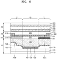
- FIG. 6 is a cross-sectional view of an organic light emitting display apparatus according to some example embodiments.
- the structure illustrated in FIG. 6 may be the same as or similar to the structure of FIG. 3 and may also be the same as the structure of FIG. 3 in that the dielectric constant of the second dielectric constant portion 202 b is set to be higher than the dielectric constant of the first dielectric constant portion 202 a of the sensitivity compensation layer 202 .
- the transparent organic layer 320 of the light blocking layer 300 may cover the first black matrix 311 but may not cover the second black matrix 312 , and the second black matrix 312 and the transparent organic layer 320 may have about the same thickness. That is, as in FIG. 4 , the transparent organic layer 320 may not have to be formed over the entire region of the light blocking layer 300 .
- the sensitivity compensation layer 202 including the first and second dielectric constant portions 202 a and 202 b having different dielectric constants may be formed in the touch screen layer 200 to correct the touch sensitivity difference in the first and second non-emission regions 11 and 12 , thereby implementing a structure ensuring a relatively stable touch operation (e.g., a touch input operation in which touch sensitivity is consistent between different areas or regions).
- the problem of the touch sensitivity difference in each region may be corrected by the differentiation of the dielectric constant of the sensitivity compensation layer, a touch operation may be smoothly performed and thus the performance and reliability of the product may be improved.
Landscapes
- Engineering & Computer Science (AREA)
- General Engineering & Computer Science (AREA)
- Theoretical Computer Science (AREA)
- Physics & Mathematics (AREA)
- Human Computer Interaction (AREA)
- General Physics & Mathematics (AREA)
- Manufacturing & Machinery (AREA)
- Optics & Photonics (AREA)
- Microelectronics & Electronic Packaging (AREA)
- Electroluminescent Light Sources (AREA)
Abstract
Description
Claims (18)
Applications Claiming Priority (2)
| Application Number | Priority Date | Filing Date | Title |
|---|---|---|---|
| KR1020190125683A KR102808663B1 (en) | 2019-10-10 | 2019-10-10 | Organic light emitting display apparatus and manufacturing method thoreof |
| KR10-2019-0125683 | 2019-10-10 |
Publications (2)
| Publication Number | Publication Date |
|---|---|
| US20210109610A1 US20210109610A1 (en) | 2021-04-15 |
| US11221694B2 true US11221694B2 (en) | 2022-01-11 |
Family
ID=75382841
Family Applications (1)
| Application Number | Title | Priority Date | Filing Date |
|---|---|---|---|
| US16/906,884 Active 2040-07-10 US11221694B2 (en) | 2019-10-10 | 2020-06-19 | Organic light emitting display apparatus and method of manufacturing the same |
Country Status (2)
| Country | Link |
|---|---|
| US (1) | US11221694B2 (en) |
| KR (1) | KR102808663B1 (en) |
Families Citing this family (1)
| Publication number | Priority date | Publication date | Assignee | Title |
|---|---|---|---|---|
| KR20220158909A (en) * | 2021-05-24 | 2022-12-02 | 삼성디스플레이 주식회사 | Electronic device |
Citations (6)
| Publication number | Priority date | Publication date | Assignee | Title |
|---|---|---|---|---|
| US20110193786A1 (en) * | 2010-02-08 | 2011-08-11 | Sony Ericsson Mobile Communications Ab | Touchscreen displays for an electronic device that include separate carbon nanotube layers for determining location and force, respectively |
| US20170185203A1 (en) | 2015-12-23 | 2017-06-29 | Samsung Display Co., Ltd. | Display device |
| US20180061899A1 (en) | 2016-08-31 | 2018-03-01 | Lg Display Co., Ltd. | Organic Light Emitting Display Having Touch Sensor and Method of Fabricating the Same |
| US20180059858A1 (en) * | 2016-08-31 | 2018-03-01 | Innolux Corporation | Touch display device |
| US20180212051A1 (en) * | 2017-01-25 | 2018-07-26 | Innolux Corporation | Conductive layer structures for substrates |
| US20190088906A1 (en) | 2017-09-20 | 2019-03-21 | Samsung Display Co., Ltd. | Display device |
-
2019
- 2019-10-10 KR KR1020190125683A patent/KR102808663B1/en active Active
-
2020
- 2020-06-19 US US16/906,884 patent/US11221694B2/en active Active
Patent Citations (8)
| Publication number | Priority date | Publication date | Assignee | Title |
|---|---|---|---|---|
| US20110193786A1 (en) * | 2010-02-08 | 2011-08-11 | Sony Ericsson Mobile Communications Ab | Touchscreen displays for an electronic device that include separate carbon nanotube layers for determining location and force, respectively |
| US20170185203A1 (en) | 2015-12-23 | 2017-06-29 | Samsung Display Co., Ltd. | Display device |
| US20180061899A1 (en) | 2016-08-31 | 2018-03-01 | Lg Display Co., Ltd. | Organic Light Emitting Display Having Touch Sensor and Method of Fabricating the Same |
| US20180059858A1 (en) * | 2016-08-31 | 2018-03-01 | Innolux Corporation | Touch display device |
| US20180212051A1 (en) * | 2017-01-25 | 2018-07-26 | Innolux Corporation | Conductive layer structures for substrates |
| US20190088906A1 (en) | 2017-09-20 | 2019-03-21 | Samsung Display Co., Ltd. | Display device |
| KR20190033118A (en) | 2017-09-20 | 2019-03-29 | 삼성디스플레이 주식회사 | Display device |
| US10476038B2 (en) | 2017-09-20 | 2019-11-12 | Samsung Display Co., Ltd. | Display device |
Also Published As
| Publication number | Publication date |
|---|---|
| KR102808663B1 (en) | 2025-05-16 |
| US20210109610A1 (en) | 2021-04-15 |
| KR20210043062A (en) | 2021-04-21 |
Similar Documents
| Publication | Publication Date | Title |
|---|---|---|
| US10886353B2 (en) | Organic light-emitting display apparatus and method of manufacturing the same | |
| US11605682B2 (en) | OLED display panel and electronic device having the same | |
| US11744121B2 (en) | Display substrate, method for manufacturing same, and display device | |
| US10069113B2 (en) | Organic light emitting display device and fabricating method using the same | |
| US10026926B2 (en) | Flexible organic light emitting diode display device and method of fabricating the same | |
| US9231035B2 (en) | Organic light emitting diode display device having improved effective emitting area | |
| JP7520188B2 (en) | Display device and manufacturing method thereof | |
| US20180233698A1 (en) | Display device | |
| TWI628822B (en) | Display device and method of manufacturing display device | |
| US11974460B2 (en) | Display substrate and method of manufacturing the same, and display device | |
| US11398185B2 (en) | Display panel, control method thereof, and display device | |
| CN112068732B (en) | A display panel and display device | |
| CN105097877A (en) | Transparent display device and manufacturing method thereof | |
| US20210233988A1 (en) | Display substrate, method for manufacturing display substrate, display panel and display device | |
| US9887377B2 (en) | Array substrate, display panel and display device having the same, and fabricating method thereof | |
| US20180286932A1 (en) | OLED Array Substrate, Manufacturing Method thereof, OLED Display Panel | |
| US10103203B2 (en) | Display unit and electronic apparatus | |
| US12133435B2 (en) | Display panel and manufacturing method thereof and display apparatus | |
| US9185796B2 (en) | Organic light emitting diode display and manufacuring method thereof | |
| KR20090094745A (en) | Display device and electronic device | |
| US11221694B2 (en) | Organic light emitting display apparatus and method of manufacturing the same | |
| US9455405B2 (en) | Organic light-emitting diode (OLED) display and method of manufacturing the same | |
| CN111386614A (en) | Light emitting diode and its manufacturing method, array substrate and display panel | |
| US11024825B2 (en) | Array substrate, method for manufacturing the same, and display device | |
| KR20240001794A (en) | Apparatus for manufacturing a display device, mask assembly and method for manufacturing a display device |
Legal Events
| Date | Code | Title | Description |
|---|---|---|---|
| AS | Assignment |
Owner name: SAMSUNG DISPLAY CO., LTD., KOREA, REPUBLIC OF Free format text: ASSIGNMENT OF ASSIGNORS INTEREST;ASSIGNORS:JUNG, JINWHAN;LEE, HYEONBUM;REEL/FRAME:052993/0013 Effective date: 20200615 |
|
| FEPP | Fee payment procedure |
Free format text: ENTITY STATUS SET TO UNDISCOUNTED (ORIGINAL EVENT CODE: BIG.); ENTITY STATUS OF PATENT OWNER: LARGE ENTITY |
|
| STPP | Information on status: patent application and granting procedure in general |
Free format text: DOCKETED NEW CASE - READY FOR EXAMINATION |
|
| STPP | Information on status: patent application and granting procedure in general |
Free format text: NOTICE OF ALLOWANCE MAILED -- APPLICATION RECEIVED IN OFFICE OF PUBLICATIONS |
|
| STPP | Information on status: patent application and granting procedure in general |
Free format text: PUBLICATIONS -- ISSUE FEE PAYMENT VERIFIED |
|
| STCF | Information on status: patent grant |
Free format text: PATENTED CASE |
|
| MAFP | Maintenance fee payment |
Free format text: PAYMENT OF MAINTENANCE FEE, 4TH YEAR, LARGE ENTITY (ORIGINAL EVENT CODE: M1551); ENTITY STATUS OF PATENT OWNER: LARGE ENTITY Year of fee payment: 4 |