US11218651B2 - Image sensor package - Google Patents
Image sensor package Download PDFInfo
- Publication number
- US11218651B2 US11218651B2 US16/786,472 US202016786472A US11218651B2 US 11218651 B2 US11218651 B2 US 11218651B2 US 202016786472 A US202016786472 A US 202016786472A US 11218651 B2 US11218651 B2 US 11218651B2
- Authority
- US
- United States
- Prior art keywords
- image sensor
- adhesive film
- substrate
- sensor chip
- sensor package
- Prior art date
- Legal status (The legal status is an assumption and is not a legal conclusion. Google has not performed a legal analysis and makes no representation as to the accuracy of the status listed.)
- Active
Links
Images


Classifications
-
- H—ELECTRICITY
- H04—ELECTRIC COMMUNICATION TECHNIQUE
- H04N—PICTORIAL COMMUNICATION, e.g. TELEVISION
- H04N5/00—Details of television systems
- H04N5/30—Transforming light or analogous information into electric information
- H04N5/33—Transforming infrared radiation
-
- H—ELECTRICITY
- H10—SEMICONDUCTOR DEVICES; ELECTRIC SOLID-STATE DEVICES NOT OTHERWISE PROVIDED FOR
- H10F—INORGANIC SEMICONDUCTOR DEVICES SENSITIVE TO INFRARED RADIATION, LIGHT, ELECTROMAGNETIC RADIATION OF SHORTER WAVELENGTH OR CORPUSCULAR RADIATION
- H10F39/00—Integrated devices, or assemblies of multiple devices, comprising at least one element covered by group H10F30/00, e.g. radiation detectors comprising photodiode arrays
- H10F39/80—Constructional details of image sensors
- H10F39/804—Containers or encapsulations
-
- H—ELECTRICITY
- H10—SEMICONDUCTOR DEVICES; ELECTRIC SOLID-STATE DEVICES NOT OTHERWISE PROVIDED FOR
- H10W—GENERIC PACKAGES, INTERCONNECTIONS, CONNECTORS OR OTHER CONSTRUCTIONAL DETAILS OF DEVICES COVERED BY CLASS H10
- H10W74/00—Encapsulations, e.g. protective coatings
- H10W74/01—Manufacture or treatment
- H10W74/014—Manufacture or treatment using batch processing
-
- H—ELECTRICITY
- H04—ELECTRIC COMMUNICATION TECHNIQUE
- H04N—PICTORIAL COMMUNICATION, e.g. TELEVISION
- H04N23/00—Cameras or camera modules comprising electronic image sensors; Control thereof
- H04N23/20—Cameras or camera modules comprising electronic image sensors; Control thereof for generating image signals from infrared radiation only
-
- H—ELECTRICITY
- H10—SEMICONDUCTOR DEVICES; ELECTRIC SOLID-STATE DEVICES NOT OTHERWISE PROVIDED FOR
- H10F—INORGANIC SEMICONDUCTOR DEVICES SENSITIVE TO INFRARED RADIATION, LIGHT, ELECTROMAGNETIC RADIATION OF SHORTER WAVELENGTH OR CORPUSCULAR RADIATION
- H10F39/00—Integrated devices, or assemblies of multiple devices, comprising at least one element covered by group H10F30/00, e.g. radiation detectors comprising photodiode arrays
- H10F39/011—Manufacture or treatment of image sensors covered by group H10F39/12
-
- H—ELECTRICITY
- H10—SEMICONDUCTOR DEVICES; ELECTRIC SOLID-STATE DEVICES NOT OTHERWISE PROVIDED FOR
- H10F—INORGANIC SEMICONDUCTOR DEVICES SENSITIVE TO INFRARED RADIATION, LIGHT, ELECTROMAGNETIC RADIATION OF SHORTER WAVELENGTH OR CORPUSCULAR RADIATION
- H10F39/00—Integrated devices, or assemblies of multiple devices, comprising at least one element covered by group H10F30/00, e.g. radiation detectors comprising photodiode arrays
- H10F39/10—Integrated devices
- H10F39/12—Image sensors
- H10F39/15—Charge-coupled device [CCD] image sensors
-
- H—ELECTRICITY
- H10—SEMICONDUCTOR DEVICES; ELECTRIC SOLID-STATE DEVICES NOT OTHERWISE PROVIDED FOR
- H10F—INORGANIC SEMICONDUCTOR DEVICES SENSITIVE TO INFRARED RADIATION, LIGHT, ELECTROMAGNETIC RADIATION OF SHORTER WAVELENGTH OR CORPUSCULAR RADIATION
- H10F39/00—Integrated devices, or assemblies of multiple devices, comprising at least one element covered by group H10F30/00, e.g. radiation detectors comprising photodiode arrays
- H10F39/10—Integrated devices
- H10F39/12—Image sensors
- H10F39/18—Complementary metal-oxide-semiconductor [CMOS] image sensors; Photodiode array image sensors
-
- H—ELECTRICITY
- H10—SEMICONDUCTOR DEVICES; ELECTRIC SOLID-STATE DEVICES NOT OTHERWISE PROVIDED FOR
- H10F—INORGANIC SEMICONDUCTOR DEVICES SENSITIVE TO INFRARED RADIATION, LIGHT, ELECTROMAGNETIC RADIATION OF SHORTER WAVELENGTH OR CORPUSCULAR RADIATION
- H10F39/00—Integrated devices, or assemblies of multiple devices, comprising at least one element covered by group H10F30/00, e.g. radiation detectors comprising photodiode arrays
- H10F39/80—Constructional details of image sensors
- H10F39/805—Coatings
-
- H—ELECTRICITY
- H10—SEMICONDUCTOR DEVICES; ELECTRIC SOLID-STATE DEVICES NOT OTHERWISE PROVIDED FOR
- H10F—INORGANIC SEMICONDUCTOR DEVICES SENSITIVE TO INFRARED RADIATION, LIGHT, ELECTROMAGNETIC RADIATION OF SHORTER WAVELENGTH OR CORPUSCULAR RADIATION
- H10F39/00—Integrated devices, or assemblies of multiple devices, comprising at least one element covered by group H10F30/00, e.g. radiation detectors comprising photodiode arrays
- H10F39/80—Constructional details of image sensors
- H10F39/811—Interconnections
-
- H—ELECTRICITY
- H10—SEMICONDUCTOR DEVICES; ELECTRIC SOLID-STATE DEVICES NOT OTHERWISE PROVIDED FOR
- H10P—GENERIC PROCESSES OR APPARATUS FOR THE MANUFACTURE OR TREATMENT OF DEVICES COVERED BY CLASS H10
- H10P72/00—Handling or holding of wafers, substrates or devices during manufacture or treatment thereof
- H10P72/70—Handling or holding of wafers, substrates or devices during manufacture or treatment thereof for supporting or gripping
- H10P72/74—Handling or holding of wafers, substrates or devices during manufacture or treatment thereof for supporting or gripping using temporarily an auxiliary support
- H10P72/7402—Wafer tapes, e.g. grinding or dicing support tapes
-
- H—ELECTRICITY
- H10—SEMICONDUCTOR DEVICES; ELECTRIC SOLID-STATE DEVICES NOT OTHERWISE PROVIDED FOR
- H10W—GENERIC PACKAGES, INTERCONNECTIONS, CONNECTORS OR OTHER CONSTRUCTIONAL DETAILS OF DEVICES COVERED BY CLASS H10
- H10W20/00—Interconnections in chips, wafers or substrates
- H10W20/40—Interconnections external to wafers or substrates, e.g. back-end-of-line [BEOL] metallisations or vias connecting to gate electrodes
- H10W20/41—Interconnections external to wafers or substrates, e.g. back-end-of-line [BEOL] metallisations or vias connecting to gate electrodes characterised by their conductive parts
- H10W20/42—Vias, e.g. via plugs
-
- H—ELECTRICITY
- H10—SEMICONDUCTOR DEVICES; ELECTRIC SOLID-STATE DEVICES NOT OTHERWISE PROVIDED FOR
- H10P—GENERIC PROCESSES OR APPARATUS FOR THE MANUFACTURE OR TREATMENT OF DEVICES COVERED BY CLASS H10
- H10P72/00—Handling or holding of wafers, substrates or devices during manufacture or treatment thereof
- H10P72/70—Handling or holding of wafers, substrates or devices during manufacture or treatment thereof for supporting or gripping
- H10P72/74—Handling or holding of wafers, substrates or devices during manufacture or treatment thereof for supporting or gripping using temporarily an auxiliary support
- H10P72/7416—Handling or holding of wafers, substrates or devices during manufacture or treatment thereof for supporting or gripping using temporarily an auxiliary support used during dicing or grinding
-
- H—ELECTRICITY
- H10—SEMICONDUCTOR DEVICES; ELECTRIC SOLID-STATE DEVICES NOT OTHERWISE PROVIDED FOR
- H10P—GENERIC PROCESSES OR APPARATUS FOR THE MANUFACTURE OR TREATMENT OF DEVICES COVERED BY CLASS H10
- H10P72/00—Handling or holding of wafers, substrates or devices during manufacture or treatment thereof
- H10P72/70—Handling or holding of wafers, substrates or devices during manufacture or treatment thereof for supporting or gripping
- H10P72/74—Handling or holding of wafers, substrates or devices during manufacture or treatment thereof for supporting or gripping using temporarily an auxiliary support
- H10P72/7428—Handling or holding of wafers, substrates or devices during manufacture or treatment thereof for supporting or gripping using temporarily an auxiliary support used to support diced chips prior to mounting
-
- H—ELECTRICITY
- H10—SEMICONDUCTOR DEVICES; ELECTRIC SOLID-STATE DEVICES NOT OTHERWISE PROVIDED FOR
- H10P—GENERIC PROCESSES OR APPARATUS FOR THE MANUFACTURE OR TREATMENT OF DEVICES COVERED BY CLASS H10
- H10P72/00—Handling or holding of wafers, substrates or devices during manufacture or treatment thereof
- H10P72/70—Handling or holding of wafers, substrates or devices during manufacture or treatment thereof for supporting or gripping
- H10P72/74—Handling or holding of wafers, substrates or devices during manufacture or treatment thereof for supporting or gripping using temporarily an auxiliary support
- H10P72/744—Details of chemical or physical process used for separating the auxiliary support from a device or a wafer
-
- H—ELECTRICITY
- H10—SEMICONDUCTOR DEVICES; ELECTRIC SOLID-STATE DEVICES NOT OTHERWISE PROVIDED FOR
- H10W—GENERIC PACKAGES, INTERCONNECTIONS, CONNECTORS OR OTHER CONSTRUCTIONAL DETAILS OF DEVICES COVERED BY CLASS H10
- H10W70/00—Package substrates; Interposers; Redistribution layers [RDL]
- H10W70/60—Insulating or insulated package substrates; Interposers; Redistribution layers
- H10W70/62—Insulating or insulated package substrates; Interposers; Redistribution layers characterised by their interconnections
- H10W70/65—Shapes or dispositions of interconnections
- H10W70/654—Top-view layouts
- H10W70/655—Fan-out layouts
-
- H—ELECTRICITY
- H10—SEMICONDUCTOR DEVICES; ELECTRIC SOLID-STATE DEVICES NOT OTHERWISE PROVIDED FOR
- H10W—GENERIC PACKAGES, INTERCONNECTIONS, CONNECTORS OR OTHER CONSTRUCTIONAL DETAILS OF DEVICES COVERED BY CLASS H10
- H10W70/00—Package substrates; Interposers; Redistribution layers [RDL]
- H10W70/60—Insulating or insulated package substrates; Interposers; Redistribution layers
- H10W70/67—Insulating or insulated package substrates; Interposers; Redistribution layers characterised by their insulating layers or insulating parts
- H10W70/68—Shapes or dispositions thereof
- H10W70/682—Shapes or dispositions thereof comprising holes having chips therein
-
- H—ELECTRICITY
- H10—SEMICONDUCTOR DEVICES; ELECTRIC SOLID-STATE DEVICES NOT OTHERWISE PROVIDED FOR
- H10W—GENERIC PACKAGES, INTERCONNECTIONS, CONNECTORS OR OTHER CONSTRUCTIONAL DETAILS OF DEVICES COVERED BY CLASS H10
- H10W72/00—Interconnections or connectors in packages
- H10W72/01—Manufacture or treatment
- H10W72/013—Manufacture or treatment of die-attach connectors
- H10W72/01331—Manufacture or treatment of die-attach connectors using blanket deposition
- H10W72/01336—Manufacture or treatment of die-attach connectors using blanket deposition in solid form, e.g. by using a powder or by laminating a foil
-
- H—ELECTRICITY
- H10—SEMICONDUCTOR DEVICES; ELECTRIC SOLID-STATE DEVICES NOT OTHERWISE PROVIDED FOR
- H10W—GENERIC PACKAGES, INTERCONNECTIONS, CONNECTORS OR OTHER CONSTRUCTIONAL DETAILS OF DEVICES COVERED BY CLASS H10
- H10W72/00—Interconnections or connectors in packages
- H10W72/01—Manufacture or treatment
- H10W72/0198—Manufacture or treatment batch processes
-
- H—ELECTRICITY
- H10—SEMICONDUCTOR DEVICES; ELECTRIC SOLID-STATE DEVICES NOT OTHERWISE PROVIDED FOR
- H10W—GENERIC PACKAGES, INTERCONNECTIONS, CONNECTORS OR OTHER CONSTRUCTIONAL DETAILS OF DEVICES COVERED BY CLASS H10
- H10W72/00—Interconnections or connectors in packages
- H10W72/071—Connecting or disconnecting
- H10W72/072—Connecting or disconnecting of bump connectors
-
- H—ELECTRICITY
- H10—SEMICONDUCTOR DEVICES; ELECTRIC SOLID-STATE DEVICES NOT OTHERWISE PROVIDED FOR
- H10W—GENERIC PACKAGES, INTERCONNECTIONS, CONNECTORS OR OTHER CONSTRUCTIONAL DETAILS OF DEVICES COVERED BY CLASS H10
- H10W72/00—Interconnections or connectors in packages
- H10W72/071—Connecting or disconnecting
- H10W72/073—Connecting or disconnecting of die-attach connectors
- H10W72/07331—Connecting techniques
- H10W72/07332—Compression bonding, e.g. thermocompression bonding
-
- H—ELECTRICITY
- H10—SEMICONDUCTOR DEVICES; ELECTRIC SOLID-STATE DEVICES NOT OTHERWISE PROVIDED FOR
- H10W—GENERIC PACKAGES, INTERCONNECTIONS, CONNECTORS OR OTHER CONSTRUCTIONAL DETAILS OF DEVICES COVERED BY CLASS H10
- H10W72/00—Interconnections or connectors in packages
- H10W72/071—Connecting or disconnecting
- H10W72/073—Connecting or disconnecting of die-attach connectors
- H10W72/07331—Connecting techniques
- H10W72/07337—Connecting techniques using a polymer adhesive, e.g. an adhesive based on silicone or epoxy
-
- H—ELECTRICITY
- H10—SEMICONDUCTOR DEVICES; ELECTRIC SOLID-STATE DEVICES NOT OTHERWISE PROVIDED FOR
- H10W—GENERIC PACKAGES, INTERCONNECTIONS, CONNECTORS OR OTHER CONSTRUCTIONAL DETAILS OF DEVICES COVERED BY CLASS H10
- H10W72/00—Interconnections or connectors in packages
- H10W72/071—Connecting or disconnecting
- H10W72/074—Connecting or disconnecting of anisotropic conductive adhesives
-
- H—ELECTRICITY
- H10—SEMICONDUCTOR DEVICES; ELECTRIC SOLID-STATE DEVICES NOT OTHERWISE PROVIDED FOR
- H10W—GENERIC PACKAGES, INTERCONNECTIONS, CONNECTORS OR OTHER CONSTRUCTIONAL DETAILS OF DEVICES COVERED BY CLASS H10
- H10W72/00—Interconnections or connectors in packages
- H10W72/071—Connecting or disconnecting
- H10W72/075—Connecting or disconnecting of bond wires
- H10W72/07551—Connecting or disconnecting of bond wires characterised by changes in properties of the bond wires during the connecting
- H10W72/07554—Connecting or disconnecting of bond wires characterised by changes in properties of the bond wires during the connecting changes in dispositions
-
- H—ELECTRICITY
- H10—SEMICONDUCTOR DEVICES; ELECTRIC SOLID-STATE DEVICES NOT OTHERWISE PROVIDED FOR
- H10W—GENERIC PACKAGES, INTERCONNECTIONS, CONNECTORS OR OTHER CONSTRUCTIONAL DETAILS OF DEVICES COVERED BY CLASS H10
- H10W72/00—Interconnections or connectors in packages
- H10W72/20—Bump connectors, e.g. solder bumps or copper pillars; Dummy bumps; Thermal bumps
- H10W72/241—Dispositions, e.g. layouts
- H10W72/244—Dispositions, e.g. layouts relative to underlying supporting features, e.g. bond pads, RDLs or vias
-
- H—ELECTRICITY
- H10—SEMICONDUCTOR DEVICES; ELECTRIC SOLID-STATE DEVICES NOT OTHERWISE PROVIDED FOR
- H10W—GENERIC PACKAGES, INTERCONNECTIONS, CONNECTORS OR OTHER CONSTRUCTIONAL DETAILS OF DEVICES COVERED BY CLASS H10
- H10W72/00—Interconnections or connectors in packages
- H10W72/20—Bump connectors, e.g. solder bumps or copper pillars; Dummy bumps; Thermal bumps
- H10W72/29—Bond pads specially adapted therefor
-
- H—ELECTRICITY
- H10—SEMICONDUCTOR DEVICES; ELECTRIC SOLID-STATE DEVICES NOT OTHERWISE PROVIDED FOR
- H10W—GENERIC PACKAGES, INTERCONNECTIONS, CONNECTORS OR OTHER CONSTRUCTIONAL DETAILS OF DEVICES COVERED BY CLASS H10
- H10W72/00—Interconnections or connectors in packages
- H10W72/30—Die-attach connectors
- H10W72/321—Structures or relative sizes of die-attach connectors
- H10W72/325—Die-attach connectors having a filler embedded in a matrix
-
- H—ELECTRICITY
- H10—SEMICONDUCTOR DEVICES; ELECTRIC SOLID-STATE DEVICES NOT OTHERWISE PROVIDED FOR
- H10W—GENERIC PACKAGES, INTERCONNECTIONS, CONNECTORS OR OTHER CONSTRUCTIONAL DETAILS OF DEVICES COVERED BY CLASS H10
- H10W72/00—Interconnections or connectors in packages
- H10W72/30—Die-attach connectors
- H10W72/351—Materials of die-attach connectors
- H10W72/352—Materials of die-attach connectors comprising metals or metalloids, e.g. solders
-
- H—ELECTRICITY
- H10—SEMICONDUCTOR DEVICES; ELECTRIC SOLID-STATE DEVICES NOT OTHERWISE PROVIDED FOR
- H10W—GENERIC PACKAGES, INTERCONNECTIONS, CONNECTORS OR OTHER CONSTRUCTIONAL DETAILS OF DEVICES COVERED BY CLASS H10
- H10W72/00—Interconnections or connectors in packages
- H10W72/30—Die-attach connectors
- H10W72/351—Materials of die-attach connectors
- H10W72/353—Materials of die-attach connectors not comprising solid metals or solid metalloids, e.g. ceramics
- H10W72/354—Materials of die-attach connectors not comprising solid metals or solid metalloids, e.g. ceramics comprising polymers
-
- H—ELECTRICITY
- H10—SEMICONDUCTOR DEVICES; ELECTRIC SOLID-STATE DEVICES NOT OTHERWISE PROVIDED FOR
- H10W—GENERIC PACKAGES, INTERCONNECTIONS, CONNECTORS OR OTHER CONSTRUCTIONAL DETAILS OF DEVICES COVERED BY CLASS H10
- H10W72/00—Interconnections or connectors in packages
- H10W72/50—Bond wires
- H10W72/59—Bond pads specially adapted therefor
-
- H—ELECTRICITY
- H10—SEMICONDUCTOR DEVICES; ELECTRIC SOLID-STATE DEVICES NOT OTHERWISE PROVIDED FOR
- H10W—GENERIC PACKAGES, INTERCONNECTIONS, CONNECTORS OR OTHER CONSTRUCTIONAL DETAILS OF DEVICES COVERED BY CLASS H10
- H10W72/00—Interconnections or connectors in packages
- H10W72/851—Dispositions of multiple connectors or interconnections
- H10W72/874—On different surfaces
- H10W72/884—Die-attach connectors and bond wires
-
- H—ELECTRICITY
- H10—SEMICONDUCTOR DEVICES; ELECTRIC SOLID-STATE DEVICES NOT OTHERWISE PROVIDED FOR
- H10W—GENERIC PACKAGES, INTERCONNECTIONS, CONNECTORS OR OTHER CONSTRUCTIONAL DETAILS OF DEVICES COVERED BY CLASS H10
- H10W72/00—Interconnections or connectors in packages
- H10W72/90—Bond pads, in general
- H10W72/941—Dispositions of bond pads
- H10W72/942—Dispositions of bond pads relative to underlying supporting features, e.g. bond pads, RDLs or vias
-
- H—ELECTRICITY
- H10—SEMICONDUCTOR DEVICES; ELECTRIC SOLID-STATE DEVICES NOT OTHERWISE PROVIDED FOR
- H10W—GENERIC PACKAGES, INTERCONNECTIONS, CONNECTORS OR OTHER CONSTRUCTIONAL DETAILS OF DEVICES COVERED BY CLASS H10
- H10W74/00—Encapsulations, e.g. protective coatings
- H10W74/10—Encapsulations, e.g. protective coatings characterised by their shape or disposition
- H10W74/15—Encapsulations, e.g. protective coatings characterised by their shape or disposition on active surfaces of flip-chip devices, e.g. underfills
-
- H—ELECTRICITY
- H10—SEMICONDUCTOR DEVICES; ELECTRIC SOLID-STATE DEVICES NOT OTHERWISE PROVIDED FOR
- H10W—GENERIC PACKAGES, INTERCONNECTIONS, CONNECTORS OR OTHER CONSTRUCTIONAL DETAILS OF DEVICES COVERED BY CLASS H10
- H10W76/00—Containers; Fillings or auxiliary members therefor; Seals
- H10W76/10—Containers or parts thereof
-
- H—ELECTRICITY
- H10—SEMICONDUCTOR DEVICES; ELECTRIC SOLID-STATE DEVICES NOT OTHERWISE PROVIDED FOR
- H10W—GENERIC PACKAGES, INTERCONNECTIONS, CONNECTORS OR OTHER CONSTRUCTIONAL DETAILS OF DEVICES COVERED BY CLASS H10
- H10W90/00—Package configurations
- H10W90/701—Package configurations characterised by the relative positions of pads or connectors relative to package parts
- H10W90/721—Package configurations characterised by the relative positions of pads or connectors relative to package parts of bump connectors
- H10W90/724—Package configurations characterised by the relative positions of pads or connectors relative to package parts of bump connectors between a chip and a stacked insulating package substrate, interposer or RDL
-
- H—ELECTRICITY
- H10—SEMICONDUCTOR DEVICES; ELECTRIC SOLID-STATE DEVICES NOT OTHERWISE PROVIDED FOR
- H10W—GENERIC PACKAGES, INTERCONNECTIONS, CONNECTORS OR OTHER CONSTRUCTIONAL DETAILS OF DEVICES COVERED BY CLASS H10
- H10W90/00—Package configurations
- H10W90/701—Package configurations characterised by the relative positions of pads or connectors relative to package parts
- H10W90/731—Package configurations characterised by the relative positions of pads or connectors relative to package parts of die-attach connectors
- H10W90/734—Package configurations characterised by the relative positions of pads or connectors relative to package parts of die-attach connectors between a chip and a stacked insulating package substrate, interposer or RDL
-
- H—ELECTRICITY
- H10—SEMICONDUCTOR DEVICES; ELECTRIC SOLID-STATE DEVICES NOT OTHERWISE PROVIDED FOR
- H10W—GENERIC PACKAGES, INTERCONNECTIONS, CONNECTORS OR OTHER CONSTRUCTIONAL DETAILS OF DEVICES COVERED BY CLASS H10
- H10W90/00—Package configurations
- H10W90/701—Package configurations characterised by the relative positions of pads or connectors relative to package parts
- H10W90/751—Package configurations characterised by the relative positions of pads or connectors relative to package parts of bond wires
- H10W90/754—Package configurations characterised by the relative positions of pads or connectors relative to package parts of bond wires between a chip and a stacked insulating package substrate, interposer or RDL
-
- H—ELECTRICITY
- H10—SEMICONDUCTOR DEVICES; ELECTRIC SOLID-STATE DEVICES NOT OTHERWISE PROVIDED FOR
- H10W—GENERIC PACKAGES, INTERCONNECTIONS, CONNECTORS OR OTHER CONSTRUCTIONAL DETAILS OF DEVICES COVERED BY CLASS H10
- H10W90/00—Package configurations
- H10W90/701—Package configurations characterised by the relative positions of pads or connectors relative to package parts
- H10W90/751—Package configurations characterised by the relative positions of pads or connectors relative to package parts of bond wires
- H10W90/755—Package configurations characterised by the relative positions of pads or connectors relative to package parts of bond wires between a chip and a laterally-adjacent insulating package substrate, interpose or RDL
-
- H—ELECTRICITY
- H10—SEMICONDUCTOR DEVICES; ELECTRIC SOLID-STATE DEVICES NOT OTHERWISE PROVIDED FOR
- H10W—GENERIC PACKAGES, INTERCONNECTIONS, CONNECTORS OR OTHER CONSTRUCTIONAL DETAILS OF DEVICES COVERED BY CLASS H10
- H10W99/00—Subject matter not provided for in other groups of this subclass
Definitions
- Apparatuses consistent with example embodiments relate to an image sensor package, and more particularly, to an image sensor package to which an adhesive film is applied.
- An image sensor is a device which converts one-dimensional or two-dimensional optical information into electric signals.
- the image senor may be categorized into, for example, a complementary metal oxide semiconductor (CMOS) image sensor and a charge coupled diode (CCD) image sensor.
- CMOS complementary metal oxide semiconductor
- CCD charge coupled diode
- the image sensor is used for cameras, camcorders, multimedia personal computers, and surveillance cameras, and its usage has been growing exponentially.
- epoxy polymer is used to attach an image sensor chip to a substrate. Because the substrate is coated thereon with a liquid epoxy polymer, the image sensor chip in a tilted state is attached to the substrate, which may result in a reduction in manufacturing yield.
- One or more example embodiments of the disclosure provide an image sensor package with increased yield and a semiconductor module including the same.
- an image sensor package may include: a substrate; an image sensor chip provided on the substrate; and an adhesive film provided between the image sensor chip and the substrate.
- a width of the adhesive film is equal to a width of the image sensor chip.
- an image sensor package may include: a substrate; an image sensor chip provided on the substrate; and an adhesive film provided between the image sensor chip and the substrate. Lateral surfaces of the adhesive film are coplanar with corresponding lateral surfaces of the image sensor chip in a thickness direction of the image sensor package.
- FIGS. 1A to 1H illustrate cross-sectional views describing a method of manufacturing an image sensor package according to an example embodiment
- FIG. 2A illustrates a cross-sectional view of an image sensor package according to an example embodiment
- FIG. 2B illustrates an enlarged view showing section A of FIG. 2A ;
- FIG. 3A illustrates a cross-sectional view of an image sensor package according to an example embodiment
- FIG. 3B illustrates a cross-sectional view of an image sensor package according to an example embodiment
- FIG. 3C illustrates a cross-sectional view of an image sensor package according to an example embodiment
- FIG. 3D illustrates a cross-sectional view of an image sensor package according to an example embodiment
- FIG. 3E illustrates a cross-sectional view of an image sensor package according to an example embodiment
- FIG. 3F illustrates a cross-sectional view of an image sensor package according to an example embodiment
- FIG. 3G illustrates a cross-sectional view of an image sensor package according to an example embodiment
- FIGS. 4A to 4H illustrate cross-sectional views describing a method of manufacturing an image sensor package according to an example embodiment
- FIG. 5 illustrates a cross-sectional view of an image sensor package according to an example embodiment
- FIGS. 6A to 6E illustrate cross-sectional views describing a method of manufacturing an image sensor package according to an example embodiment
- FIG. 7 illustrates a cross-sectional view of an image sensor package according to an example embodiment.
- FIGS. 1A to 1H illustrate cross-sectional views describing a method of manufacturing an image sensor package according to an example embodiment.
- a first base film 100 a may be prepared.
- a first fixing ring 500 may be attached to opposite ends of the first base film 100 a .
- the first fixing ring 500 may serve to support the first base film 100 a .
- a first intermediate layer 200 a may be provided on a top surface of the first base film 100 a .
- the first intermediate layer 200 a may have adhesive properties. When the first intermediate layer 200 a is irradiated with an ultraviolet ray, an adhesive force of the first intermediate layer 200 a may change with a certain layer, for example, an adhesive film 300 which will be discussed below.
- An adhesive film 300 may be provided on a top surface of the first intermediate layer 200 a .
- the adhesive film 300 may be provided on a top surface of the first intermediate layer 200 a in a half-cured state. In other words, the adhesive film 300 may be in a half-solid state. Afterwards, the adhesive film 300 may be annealed and then completely cured.
- a semiconductor wafer 400 a may be provided on a top surface of the adhesive film 300 .
- the semiconductor wafer 400 a may be, for example, a silicon wafer.
- the semiconductor wafer 400 a and the adhesive film 300 may be attached to each other.
- Chip connection pads 50 may be provided on a top surface of the semiconductor wafer 400 a .
- the chip connection pads 50 may include a conductive material.
- the semiconductor wafer 400 a may be diced to form a plurality of image sensor chips 400 b and grooves 600 .
- the adhesive film 300 and the first intermediate layer 200 a may also be diced together with the semiconductor wafer 400 a .
- the grooves 600 may penetrate through the adhesive film 300 , the first intermediate layer 200 a , and an upper portion of the first base film 100 a .
- the bottom surfaces of the grooves 600 may be provided in the first base film 100 a .
- a lower portion of the first base film 100 a may not be diced.
- the adhesive film 300 may have lateral surfaces 300 c coplanar with lateral surfaces 400 c of the image sensor chip 400 b .
- a width W 1 of the image sensor chip 400 b may be equal to a width W 2 of the adhesive film 300 .
- the image sensor chip 400 b may have the same area as that of the adhesive film 300 .
- the first intermediate layer 200 a may be irradiated with an ultraviolet ray.
- An adhesive force between the first intermediate layer 200 a and the adhesive film 300 may be reduced after the first intermediate layer 200 a is exposed to the ultraviolet ray.
- a chip collector 700 may be provided on a top surface of one of the image sensor chips 400 b of the plurality of image sensor chips 400 b .
- the chip collector 700 may grip onto the top surface of the image sensor chip 400 b , and may lift up the image sensor chip 400 b .
- the chip collector 700 may also transport one of the adhesive films 300 that is in contact with the image sensor chip 400 b . The following will describe movement of the image sensor chip 400 b and its corresponding adhesive film 300 .
- the first intermediate layer 200 a and the adhesive film 300 may be separated from each other in a vertical direction (i.e., in a thickness direction of the first intermediate layer 200 a and the adhesive film 300 ). Thereafter, the chip collector 700 may convey the image sensor chip 400 b and the adhesive film 300 detached from the first intermediate layer 200 a to a desired position.
- An ejector pin 800 may be provided on a bottom surface (opposite to the top surface on which the chip collector 700 is provided) of the first base film 100 a . The ejector pin 800 may grip onto the bottom surface of the first base film 100 a , and may assist the first intermediate layer 200 a and the adhesive film 300 to be separated from each other in the vertical direction.
- the image sensor chip 400 b may experience stress due to an action of the ejector pin 800 .
- the adhesive film 300 may be interposed between the first base film 100 a and a bottom surface of the image sensor chip 400 b , and thus the stress may be alleviated.
- an image sensor package may employ the image sensor chip 400 b having a small thickness.
- the employment of the thin image sensor chip 400 b may reduce a thickness of the image sensor package and may also achieve compactness of products.
- a second base film 100 b may be prepared.
- the second base film 100 b may be an individual component separated from the first base film 100 a .
- a second intermediate layer 200 b may be provided on a top surface of the second base film 100 b .
- the second intermediate layer 200 b may be an individual component separated from the first intermediate layer 200 a .
- a second fixing ring 502 may be attached to opposite ends of the second intermediate layer 200 b .
- the image sensor chip 400 b and the adhesive film 300 that are held by the chip collector 700 as discussed in FIG. 1C may move toward a top surface of the second intermediate layer 200 b , and then the image sensor chip 400 b and the adhesive film 300 may be provided on a top surface of the second intermediate layer 200 b .
- the chip collector 700 may also transport the adhesive film 300 attached to the image sensor chip 400 b .
- the movement of the image sensor chip 400 b and its corresponding adhesive film 300 may be repeatedly performed on a plurality of image sensor chips 400 b and a plurality of adhesive films 300 attached respectively thereto.
- the second intermediate layer 200 b may be irradiated with an ultraviolet ray. Thereby, an adhesive force between the second intermediate layer 200 b and the adhesive film 300 may be reduced after the second intermediate layer 200 b is exposed to the ultraviolet ray.
- the chip collector 700 may hold onto a top surface of a specific one of the image sensor chips 400 b , and may lift up the specific image sensor chip 400 b .
- the chip collector 700 may transport one of the adhesive films 300 that is in contact with the specific image sensor chip 400 b . Therefore, the second intermediate layer 200 b and the adhesive film 300 may be separated from each other in the vertical direction.
- the chip collector 700 may covey the image sensor chip 400 b (along with the adhesive film 300 ) to a desired position.
- the ejector pin 800 may act identically to that discussed in FIG. 1C .
- a description overlapping with that discussed in FIG. 1C will be omitted to avoid redundancy.
- a substrate 10 may be prepared. Upper substrate pads 20 may be provided on a top surface of the substrate 10 . Lower substrate pads 24 may be provided on a bottom surface of the substrate 10 .
- the substrate 10 may include connectors 22 therein to connect the upper substrate pads 20 and the lower substrate pads 24 .
- External terminals 30 may be provided on bottom surfaces of the lower substrate pads 24 .
- the image sensor chip 400 b held by the chip collector 700 as discussed in FIG. 1E may be transferred onto the top surface of the substrate 10 , and then the substrate 10 may be provided thereon with the image sensor chip 400 b .
- the chip collector 700 may also transport one of the adhesive films 300 that is in contact with the image sensor chip 400 b .
- the adhesive film 300 may be interposed between the image sensor chip 400 b and the substrate 10 .
- the adhesive film 300 may attach the image sensor chip 400 b to the top surface of the substrate 10 . Accordingly, the image sensor chip 400 b may be fixed to the top surface of the substrate 10 .
- bonding wires 40 may be provided on the top surface of the substrate 10 to be connected to the chip connection pads 50 at one end and the upper substrate pads 20 at the other end.
- the substrate 10 may be diced to form a plurality of image sensor packages 1 a .
- Each of the plurality of image sensor packages 1 a may include the substrate 10 , the adhesive film 300 , and the image sensor chip 400 b.
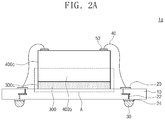
- FIG. 2A illustrates a cross-sectional view of an image sensor package 1 a according to an example embodiment.
- FIG. 2B illustrates an enlarged view showing section A of FIG. 2A .
- an image sensor package 1 a may include a substrate 10 , an adhesive film 300 , an image sensor chip 400 b , and bonding wires 40 .
- the image sensor package 1 a may be manufactured as discussed above in conjunction with FIGS. 1A to 1H .
- the substrate 10 may be, for example, a printed circuit board (PCB).
- the substrate 10 may be provided with upper substrate pads 20 on a top surface thereof.
- the substrate 10 may be provided with lower substrate pads 24 on a bottom surface thereof.
- the substrate 10 may include connectors 22 therein.
- the connectors 22 may include vias and conductive patterns. The connectors 22 may penetrate the substrate 10 to electrically connect the upper substrate pads 20 and the lower substrate pads 24 to each other.
- External terminals 30 may be provided on a respective bottom surface of the lower substrate pads 24 .
- the external terminals 30 may have, for example, a solder-ball shape.
- the upper substrate pads 20 , the lower substrate pads 24 , the connectors 22 , and the external terminals 30 may be made up of a conductive material for electric conduction.
- the conductive material may include copper (Cu).
- the phrase “electrically connected/coupled to” may include “directly or indirectly electrically connected/coupled to.”
- the adhesive film 300 may be provided on the top surface of the substrate 10 .
- the adhesive film 300 may be interposed between the substrate 10 and the image sensor chip 400 b .
- the adhesive film 300 may have lateral surfaces 300 c coplanar with corresponding lateral surfaces 400 c of the image sensor chip 400 b along a thickness direction of the image sensor package 1 a .
- the adhesive film 300 may have the same area as that of the image sensor chip 400 b .
- the adhesive film 300 may include one or more of an adhesive polymer, a thermosetting polymer, and a dielectric polymer.
- the adhesive film 300 may include an epoxy-based polymer and silica.
- the adhesive film 300 may have a glass transition temperature (Tg) ranging from about 140° C.
- the adhesive film 300 may be provided in a half-cured state.
- the adhesive film 300 may serve to attach and fix the image sensor chip 400 b to the substrate 10 .
- the adhesive film 300 may be annealed and then cured, and as a result, the image sensor chip 400 b may be securely fixed to the substrate 10 .
- the adhesive film 300 may have a thermal expansion coefficient less than that of an epoxy-based polymer. The higher a thermal expansion coefficient, the greater a difference H 2 between minimum and maximum thicknesses H 1 and H 3 of the adhesive film 300 at opposite sides of the image sensor package 1 a .
- the difference H 2 between the minimum and maximum thicknesses H 1 and H 3 of the adhesive film 300 may accelerate a tilting phenomenon of the image sensor chip 400 b .
- the tiling phenomenon of the image sensor chip 400 b may be reduced in comparison with a case where an epoxy-based polymer is used.
- a tilting degree of the image sensor chip 400 b may be proportional to a ratio of the maximum thickness H 3 to the minimum thickness H 1 of the adhesive film 300 at opposite sides of the image sensor package 1 a .
- the ratio of the maximum thickness H 3 to the minimum thickness H 1 of the adhesive film 300 may be in a range of about 1 to about 1.15.
- the image sensor chip 400 b may be slightly tilted to increase manufacturing yield.
- the image sensor chip 400 b may be provided on a top surface of the adhesive film 300 .
- the image sensor chip 400 b may include a complementary metal oxide semiconductor (CMOS) image sensor chip, or CIS(CMOS Image Sensor) chip.
- CMOS complementary metal oxide semiconductor
- CIS(CMOS Image Sensor) chip CIS(CMOS Image Sensor) chip.
- the image sensor chip 400 b may sense objects and output electric signals according to the sensed objects.
- the image sensor chip 400 b may include therein a circuit layer and the circuit layer may include integrated circuits.
- the electric signals output from the image sensor chip 400 b may be transmitted through the bonding wires 40 to the substrate 10 .
- Chip connection pads 50 may be provided on, for example, an edge region of a top surface of the image sensor chip 400 b .
- the chip connection pads 50 may be made up of metal, for example, aluminum (Al).
- the bonding wires 40 may contact the chip connection pads 50 at one end and the upper substrate pads 20 at the other end.
- the bonding wires 40 may be disposed adjacent to the lateral surfaces 400 c of the image sensor chip 400 b .
- the image sensor chip 400 b may be electrically connected through the bonding wires 40 to the substrate 10 .
- the bonding wires 40 may include a conductive material, for example, gold (Au), aluminum (Al), copper (Cu), or a combination thereof.
- FIG. 3A illustrates a cross-sectional view of an image sensor package 1 b according to an example embodiment.
- an image sensor package 1 b may include a substrate 10 , an adhesive film 300 , an image sensor chip 400 b , bonding wires 40 , a holder 60 , and an infrared filter 70 .
- the substrate 10 , the adhesive film 300 , the image sensor chip 400 b , and the bonding wires 40 may be the same as those discussed in FIGS. 2A and 2B . Thus, duplicate descriptions of those elements will be omitted below.
- the holder 60 may be provided on the substrate 10 .
- the holder 60 may include a leg 61 and a body 62 .
- the leg 61 may be provided on an edge region of a top surface of the substrate 10 , surrounding the image sensor chip 400 b .
- the body 62 may be provided over the substrate 10 and a top surface of the image sensor chip 400 b .
- the leg 61 and the body 62 may be integrally connected to constitute the holder 60 .
- the body 62 of the holder 60 may support the infrared filter 70 .
- the holder 60 may surround the image sensor chip 400 b and protect the image sensor chip 400 b against external impact or foreign object.
- the holder 60 may be made up of a polymer, for example, an epoxy-based polymer.
- the infrared filter 70 may be provided over the top surface of the image sensor chip 400 b .
- the infrared filter 70 may be provided on a top surface of the body 62 of the holder 60 .
- the infrared filter 70 may be vertically spaced apart from and may face the image sensor chip 400 b .
- the infrared filter 70 may overlap the image sensor chip 400 b along a vertical direction of the image sensor package 1 b .
- the infrared filter 70 may selectively allow light to pass therethrough.
- the infrared filter 70 may filter out an infrared ray amongst incident light.
- the top surface of the image sensor chip 400 b may be exposed to light that passes through the infrared filter 70 .
- An empty space 80 may be formed between the infrared filter 70 and the image sensor chip 400 b .
- the empty space 80 may also be provided laterally between an inner sidewall 60 c of the leg 61 and the lateral surfaces 400 c of the image sensor chip 400 b.
- FIG. 3B illustrates a cross-sectional view of an image sensor package 1 c according to an example embodiment.
- an image sensor package 1 c may include a substrate 10 , an adhesive film 300 , an image sensor chip 400 b , bonding wires 40 , a holder 60 , and an infrared filter 70 .
- the adhesive film 300 , the image sensor chip 400 b , and the bonding wires 40 may be the same as those discussed in FIGS. 2A and 2B .
- the holder 60 and the infrared filter 70 may be the same as those discussed in FIG. 3A . Thus, duplicate descriptions of those elements will be omitted below.
- the substrate 10 may include connectors 22 ′ therein.
- the connectors 22 ′ may include vias and conductive patterns.
- the connectors 22 ′ may electrically connect the upper substrate pads 20 to a flexible substrate connectors 26 .
- At least one external terminal 30 ′ may be provided on one of top and bottom surfaces of a connection substrate 14 .
- the connection substrate 14 may include a connection substrate connectors 28 .
- the connection substrate connector 28 may electrically connect the external terminal 30 ′ to the flexible substrate connector 26 .
- the connection substrate connector 28 and the external terminal 30 ′ may be made up of a conductive material.
- a flexible substrate 12 may be provided between the substrate 10 and the connection substrate 14 .
- the flexible substrate 12 may have one end coupled to one side of the substrate 10 and the other end coupled to one side of the connection substrate 14 .
- the flexible substrate 12 may be made up of a dielectric polymer.
- the flexible substrate 12 may be made up of a polyimide-based polymer.
- the flexible substrate 12 may include the flexible substrate connector 26 therein. The flexible substrate 12 may be readily bent. When the flexible substrate 12 is bent, the flexible substrate connector 26 provided in the flexible substrate 12 may also be bent.
- the flexible substrate connector 26 may have one end coupled to the connectors 22 ′ and the other end coupled to the connection substrate connector 28 .
- the flexible substrate connector 26 may electrically connect the connectors 22 ′ to the connection substrate connector 28 .
- electric signals provided from the image sensor chip 400 b may be externally output through the chip connection pads 50 , the bonding wires 40 , the upper substrate pads 20 , the connectors 22 ′, the flexible substrate connector 26 , the connection substrate connector 28 , and the external terminal 30 ′, in that order.
- FIG. 3C illustrates a cross-sectional view of an image sensor package 1 d according to an example embodiment.
- an image sensor package 1 d may include a substrate 10 , an adhesive film 300 , an image sensor chip 400 b , bonding wires 40 , a molding layer 90 , a filter supporter 65 , and an infrared filter 70 .
- the substrate 10 , the adhesive film 300 , the image sensor chip 400 b , and the bonding wires 40 may be the same as those discussed in FIGS. 2A and 2B .
- the infrared filter 70 may be the same as that discussed in FIG. 3A . Thus, duplicate descriptions of these elements will be omitted below.
- the molding layer 90 may be provided on the substrate 10 and may cover the lateral surfaces 300 c of the adhesive film 300 , the lateral surfaces 400 c of the image sensor chip 400 b , and the edge region of the top surface of the image sensor chip 400 b .
- the molding layer 90 may thus encapsulate the chip connection pads 50 and the bonding wires 40 .
- the molding layer 90 does not cover a central portion of the image sensor chip 400 b , the image sensor chip 400 b may be exposed to light that passes through the infrared filter 70 .
- the molding layer 90 may include a dielectric polymer, for example, an epoxy-based polymer. The molding layer 90 may protect the image sensor chip 400 b and the bonding wires 40 against external impact and foreign object.
- the filter supporter 65 may be provided on a top surface of the molding layer 90 and support the infrared filter 70 .
- the filter supporter 65 may fix the infrared filter 70 .
- the substrate 10 may be replaced with the substrate 10 , the flexible substrate 12 , and the connection substrate 14 discussed in FIG. 3B .
- FIG. 3D illustrates a cross-sectional view of an image sensor package 1 e according to an example embodiment.
- an image sensor package 1 e may include a substrate 10 , an adhesive film 300 , an image sensor chip 400 b , bonding wires 40 , a molding layer 90 , and an infrared filter 70 .
- the substrate 10 , the adhesive film 300 , the image sensor chip 400 b , and the bonding wires 40 may be the same as those discussed in FIGS. 2A and 2B .
- the molding layer 90 may be the same as that discussed in FIG. 3C . Thus, duplicate descriptions of those features will be omitted below.
- the infrared filter 70 may be provided over a top surface of the image sensor chip 400 b .
- the infrared filter 70 may be vertically spaced apart from and may face the image sensor chip 400 b .
- the infrared filter 70 may have a bottom surface 70 b located at a lower level than that of a top surface 90 a of the molding layer 90 . Accordingly, it may be possible to reduce a height of the image sensor package 1 e and to achieve compactness of an image sensor package.
- the empty space 80 may be formed between the infrared filter 70 and the image sensor chip 400 b .
- the empty space 80 may also be surrounded by an inner sidewall 90 c of the molding layer 90 .
- the substrate 10 may be replaced with the substrate 10 , the flexible substrate 12 , and the connection substrate 14 discussed in FIG. 3B .
- FIG. 3E illustrates a cross-sectional view showing an image sensor package 1 f according to an example embodiment.
- an image sensor package 1 f may include a substrate 10 , an adhesive film 300 , an image sensor chip 400 b , bonding wires 40 , a molding layer 90 , and an infrared filter 70 .
- the substrate 10 , the adhesive film 300 , the image sensor chip 400 b , and the bonding wires 40 may be the same as those discussed in FIGS. 2A and 2B .
- the molding layer 90 may be the same as that discussed in FIG. 3C or 3D . Thus, duplicate descriptions of these features will be omitted below.
- the infrared filter 70 may be provided on the top surface of the image sensor chip 400 b .
- the infrared filter 70 may have a bottom surface in direct contact with the top surface of the image sensor chip 400 b .
- the infrared filter 70 may cover the central portion of the image sensor chip 400 b .
- the infrared filter 70 may have a top surface 70 a provided at a position lower than the top surface 90 a of the molding layer 90 and higher than the top surface of the image sensor chip 400 b .
- the infrared filter 70 may have lateral surfaces 70 c in contact with the inner sidewall 90 c of the molding layer 90 .
- the substrate 10 may be replaced with the substrate 10 , the flexible substrate 12 , and the connection substrate 14 discussed in FIG. 3B .
- FIG. 3F illustrates a cross-sectional view of an image sensor package 1 g according to an example embodiment.
- an image sensor package 1 g may include a substrate 10 , a stiffener 15 , an adhesive film 300 , an image sensor chip 400 b , bonding wires 40 , a holder 60 , and an infrared filter 70 .
- the adhesive film 300 , the image sensor chip 400 b , and the bonding wires 40 may be the same as those discussed in FIGS. 2A and 2B .
- the holder 60 and the infrared filter 70 may be the same as those discussed in FIG. 3A or 3B . Thus, duplicate descriptions of these features will be omitted below.
- the stiffener 15 may be prepared.
- the stiffener 15 may include a stainless steel.
- the stiffener 15 may serve to support the substrate 10 and the image sensor chip 400 b.
- the substrate 10 may be provided on a top surface of the stiffener 15 .
- the substrate 10 may be a printed circuit board (PCB).
- the substrate 10 may have a hole 11 penetrating the top and bottom surfaces thereof.
- the hole 11 may provide a cavity CV inside the substrate 10 .
- the cavity CV may be spatially connected to the empty space 80 .
- the adhesive film 300 and the image sensor chip 400 b may be provided in the cavity CV on the stiffener 15 .
- the top surface of the image sensor chip 400 b may be located at a lower level than that of the top surface of the substrate 10 . Because the image sensor chip 400 b is provided in the cavity CV of the substrate 10 , it may be possible to reduce a height of the image sensor package 1 g and in turn to achieve compactness of products.
- FIG. 3G illustrates a cross-sectional view of an image sensor package 1 h according to an example embodiment.
- an image sensor package 1 h may include a substrate 10 , a stiffener 15 , an adhesive film 300 , an image sensor chip 400 b , bonding wires 40 , a holder 60 , and an infrared filter 70 .
- the adhesive film 300 , the image sensor chip 400 b , and the bonding wires 40 may be the same as those discussed in FIGS. 2A and 2B .
- the holder 60 and the infrared filter 70 may be the same as those discussed in FIG. 3A or 3B .
- the stiffener 15 may be the same as that discussed in FIG. 3F . Thus, duplicate descriptions of these features will be omitted below.
- the substrate 10 may be provided on the top surface of the stiffener 15 .
- the substrate 10 may have a hole 11 penetrating the top and bottom surfaces thereof.
- the hole 11 may provide a cavity CV in the substrate 10 .
- the adhesive film 300 and the image sensor chip 400 b may be provided in the cavity CV.
- the substrate 10 may include connectors 22 ′′ therein.
- the connectors 22 ′′ may electrically connect the upper substrate pads 20 to the flexible substrate connector 26 .
- the flexible substrate connector 26 may electrically connect the connectors 22 ′′ to the connection substrate connector 28 .
- the connection substrate connector 28 may electrically connect the flexible substrate connector 26 to the external terminal 30 ′.
- electric signals provided from the image sensor chip 400 b may be externally output through the chip connection pads 50 , the bonding wires 40 , the upper substrate pads 20 , the connectors 22 ′′, the flexible substrate connector 26 , the connection substrate connector 28 , and the external terminal 30 ′.
- FIGS. 4A to 4H illustrate cross-sectional views illustrating a method of manufacturing an image sensor package according to an example embodiment.
- a description discussed with reference to FIGS. 1A to 1H may also be identically or similarly applicable to the following embodiment illustrated in FIGS. 4A to 4H , and thus the repetitive description will be omitted to avoid redundancy.
- a first base film 100 a may be prepared.
- a first fixing ring 500 may be attached to opposite ends of the first base film 100 a .
- a first intermediate layer 200 a may be provided on a top surface of the first base film 100 a .
- An anisotropic conductive film (ACF) may be provided on a top surface of the first intermediate layer 200 a .
- the anisotropic conductive film may include an adhesive film 300 and conductive particles 302 .
- the conductive particles 302 may be provided in the adhesive film 300 .
- the conductive particles 302 may be uniformly distributed in the adhesive film 300 .
- the adhesive film 300 may be provided on a top surface of first intermediate layer 200 a in a half-cured state (or a semi-cured state).
- the adhesive film 300 may be in a half-solid state (or a semi-solid state). Afterwards, the adhesive film 300 may be annealed and then completely cured.
- a semiconductor wafer 400 a may be prepared with lower chip pads 420 and conductive vias T provided therein. The lower chip pads 420 may be provided on a bottom surface of the semiconductor wafer 400 a .
- the conductive vias T may penetrate through the semiconductor wafer 400 a .
- the conductive vias T may be vertically aligned with the lower chip pads 420 .
- the semiconductor wafer 400 a may be provided to allow its bottom surface to face the adhesive film 300 .
- the semiconductor wafer 400 a may be diced to form a plurality of image sensor chips 400 b and a plurality of grooves 600 .
- the plurality of grooves 600 may penetrate through the adhesive film 300 and the first intermediate layer 200 a.
- the first intermediate layer 200 a may be irradiated with an ultraviolet ray.
- a chip collector 700 may be provided on a top surface of one of the image sensor chips 400 b .
- the chip collector 700 may convey the image sensor chip 400 b and its attached adhesive film 300 to a desired position.
- An ejector pin 800 may be provided on a bottom surface of the first base film 100 a to further support the separation.
- the image sensor chip 400 b and the adhesive film 300 being held by the chip collector 700 as discussed in FIG. 4C may be transported toward a top surface of a second intermediate layer 200 b , and then the image sensor chip 400 b and the adhesive film 300 may be provided on the second intermediate layer 200 b.
- the second intermediate layer 200 b may be irradiated with an ultraviolet ray.
- the chip collector 700 may be provided on a top surface of an image sensor chip 400 b .
- the chip collector 700 may hold onto the top surface of the image sensor chips 400 b , and may lift up the image sensor chip 400 b.
- a substrate 10 may be prepared.
- the image sensor chip 400 b held by the chip collector 700 as discussed in FIG. 4E may be transported onto a top surface of the substrate 10 , and then the substrate 10 may be provided with the image sensor chip 400 b on the top surface thereof.
- the adhesive film 300 may also move together with the image sensor chip 400 b .
- the image sensor chip 400 b may be disposed on the substrate 10 in order to align the lower chip pads 420 with corresponding upper substrate pads 20 .
- the adhesive film 300 and the conductive particles 302 may be heated and pressurized.
- the applied heat and pressure may force the conductive particles 302 to flow and aggregate in the adhesive film 300 .
- the conductive particles 302 may aggregate between the lower chip pads 420 and the upper substrate pads 20 .
- the conductive particles 302 may aggregate to form conductors 304 .
- the conductors 304 may electrically connect the lower chip pads 420 to the upper substrate pads 20 .
- the conductors 304 may be surrounded by the adhesive film 300 .
- the substrate 10 may be diced to form image sensor packages 1 i .
- Each of the image sensor packages 1 i may include the substrate 10 , the adhesive film 300 , the conductors 304 , the conductive vias T, and the image sensor chip 400 b.
- FIG. 5 illustrates a cross-sectional view of an image sensor package 1 j according to an example embodiment.
- an image sensor package 1 j may include a substrate 10 , an adhesive film 300 , conductors 304 , an image sensor chip 400 b , a holder 60 , and an infrared filter 70 .
- the substrate 10 , the image sensor chip 400 b , the holder 60 , and the infrared filter 70 may be substantially the same as those discussed in FIG. 3A , and thus the repetitive description will be omitted below.
- the substrate 10 , the conductors 304 , the image sensor chip 400 b , and the adhesive film 300 may be manufactured as discussed above in conjunction with FIGS. 4A to 4G .
- the conductive particles 302 may aggregate such that the conductors 304 may be provided between the lower chip pads 420 and the upper substrate pads 20 .
- the conductors 304 may contact and electrically connect the lower chip pads 420 and the upper substrate pads 20 . Accordingly, electric signals provided from the image sensor chip 400 b may externally output through the conductive vias T, the lower chip pads 420 , the conductors 304 , the upper substrate pads 20 , the connectors 22 , the lower substrate pads 24 , and the external terminals 30 .
- the holder 60 may be replaced with the molding layer 90 discussed in FIG. 3C or 3D .
- the substrate 10 may be replaced with the substrate 10 , the flexible substrate 12 , and the connection substrate 14 discussed in FIG. 3B .
- FIGS. 6A to 6E illustrate cross-sectional views describing a method of manufacturing an image sensor package according to an example embodiment.
- a description discussed with reference to FIGS. 1A to 1H may also be identically or similarly applicable to the following example embodiment illustrated in FIGS. 6A to 6H , and thus the repetitive description will be omitted to avoid redundancy.
- a first base film 100 a may be prepared.
- a first fixing ring 500 may be attached to opposite ends of the first base film 100 a .
- a first intermediate layer 200 a may be provided on a top surface of the first base film 100 a .
- An adhesive film 300 may be provided on a top surface of the first intermediate layer 200 a .
- the adhesive film 300 may be a non-conductive film (NCF).
- a semiconductor wafer 400 a may be prepared with lower chip pads 420 , conductive terminals 440 , and conductive vias T formed therein.
- the lower chip pads 420 may be provided on a bottom surface of the semiconductor wafer 400 a .
- the conductive terminals 440 may be provided on bottom surfaces of the lower chip pads 420 .
- the conductive vias T may penetrate the semiconductor wafer 400 a .
- the conductive vias T may be vertically aligned with the lower chip pads 420 .
- the semiconductor wafer 400 a may be provided to allow its bottom surface to
- the semiconductor wafer 400 a may be diced to form a plurality of image sensor chips 400 b and a plurality of grooves 600 .
- the grooves 600 may penetrate through the adhesive film 300 and the first intermediate layer 200 a.
- a substrate 10 may be prepared.
- the method discussed in FIGS. 1C to 1E may be performed such that one of the image sensor chips 400 b of FIG. 6B is transported onto a top surface of the substrate 10 , and that the substrate 10 may be provided with the image sensor chip 400 b on the top surface thereof.
- One of the adhesive films 300 that is in contact with the image sensor chip 400 b may also move onto the top surface of the substrate 10 .
- the image sensor chip 400 b may be disposed to align the conductive terminals 440 with corresponding upper substrate pads 20 .
- the conductive terminals 440 may be vertically spaced apart from the upper substrate pads 20 .
- the adhesion film 300 may be interposed between the conductive terminals 440 and the upper substrate pads 20 .
- the adhesive film 300 may be heated to have fluidity.
- the image sensor chip 400 b may be provided with pressure in a direction perpendicular to a top surface of the substrate 10 . Therefore, the conductive terminals 440 may contact and have electrical connection with corresponding upper substrate pads 20 .
- the substrate 10 may be diced to form a plurality of image sensor packages 1 k .
- Each of the image sensor packages 1 k may include the substrate 10 , the adhesive film 300 , the image sensor chip 400 b , and the conductive terminals 440 .
- FIG. 7 illustrates a cross-sectional view of an image sensor package according to an example embodiment.
- an image sensor package 1 l may include a substrate 10 , an adhesive film 300 , conductive terminals 440 , an image sensor chip 400 b , a holder 60 , and an infrared filter 70 .
- the substrate 10 , the holder 60 , and the infrared filter 70 may be substantially the same as those discussed in FIG. 3A .
- the substrate 10 , the image sensor chip 400 b , the conductive terminals 440 , and the adhesive film 300 may be manufactured as discussed above in conjunction with FIGS. 6A to 6E .
- the conductive terminals 440 may be provided on top surfaces of the upper substrate pads 20 , respectively.
- the conductive terminals 440 may be positioned in the adhesive film 300 .
- the conductive terminals 440 may correspondingly contact the lower chip pads 420 and the upper substrate pads 20 .
- the conductive terminals 440 may electrically connect the lower chip pads 420 to the upper substrate pads 20 . Accordingly, electric signals provided from the image sensor chip 400 b may externally output through the conductive vias T, the lower chip pads 420 , the conductive terminals 440 , the upper substrate pads 20 , the connectors 22 , the lower substrate pads 24 , and the external terminals 30 .
- the holder 60 may be replaced with the molding layer 90 discussed in FIG. 3C or 3D .
- the substrate 10 may be replaced with the substrate 10 , the flexible substrate 12 , and the connection substrate 14 discussed in FIG. 3B .
- An image sensor package may include an adhesive film on a bottom surface of an image sensor chip. Therefore, the image sensor package may increase in performance and production yield.
Landscapes
- Engineering & Computer Science (AREA)
- Multimedia (AREA)
- Signal Processing (AREA)
- Solid State Image Pick-Up Elements (AREA)
Abstract
Description
Claims (17)
Applications Claiming Priority (2)
| Application Number | Priority Date | Filing Date | Title |
|---|---|---|---|
| KR1020190057286A KR20200133072A (en) | 2019-05-16 | 2019-05-16 | Image Sensor Package |
| KR10-2019-0057286 | 2019-05-16 |
Publications (2)
| Publication Number | Publication Date |
|---|---|
| US20200366853A1 US20200366853A1 (en) | 2020-11-19 |
| US11218651B2 true US11218651B2 (en) | 2022-01-04 |
Family
ID=73231383
Family Applications (1)
| Application Number | Title | Priority Date | Filing Date |
|---|---|---|---|
| US16/786,472 Active US11218651B2 (en) | 2019-05-16 | 2020-02-10 | Image sensor package |
Country Status (3)
| Country | Link |
|---|---|
| US (1) | US11218651B2 (en) |
| KR (1) | KR20200133072A (en) |
| CN (1) | CN111952324A (en) |
Families Citing this family (3)
| Publication number | Priority date | Publication date | Assignee | Title |
|---|---|---|---|---|
| US11912899B2 (en) * | 2021-03-24 | 2024-02-27 | Sony Group Corporation | Film, liquid paint and method |
| JP7813645B2 (en) * | 2022-04-21 | 2026-02-13 | 浜松ホトニクス株式会社 | Photodetector |
| US12590835B2 (en) * | 2022-09-27 | 2026-03-31 | Lite-On Singapore Pte. Ltd. | Electronic device and sensor package with optical functional layer thereof |
Citations (22)
| Publication number | Priority date | Publication date | Assignee | Title |
|---|---|---|---|---|
| US5448105A (en) * | 1989-09-28 | 1995-09-05 | Dia Nippon Printing Co., Ltd. | Semiconductor device having a leadframe and metal substrate |
| US6198165B1 (en) * | 1998-05-29 | 2001-03-06 | Sharp Kabushiki Kaisha | Semiconductor device |
| US6207550B1 (en) * | 1997-07-02 | 2001-03-27 | Matsushita Electric Industrial Co., Ltd. | Method for fabricating bump electrodes with a leveling step for uniform heights |
| US20030234886A1 (en) * | 2002-06-19 | 2003-12-25 | Cho Min Kyo | Image pickup device and manufacturing method thereof |
| US7071032B2 (en) | 2002-08-01 | 2006-07-04 | Taiwan Semiconductor Manufacturing Co., Ltd. | Material to improve image sensor yield during wafer sawing |
| US20070010041A1 (en) | 2005-07-11 | 2007-01-11 | Samsung Electronics Co., Ltd. | Method of manufacturing optical device having transparent cover and method of manufacturing optical device module using the same |
| US20070054984A1 (en) * | 2005-09-02 | 2007-03-08 | Jun Jung B | Insulated conductive particles and anisotropic conductive adhesive film using the same |
| US20070215992A1 (en) * | 2006-03-17 | 2007-09-20 | Geng-Shin Shen | Chip package and wafer treating method for making adhesive chips |
| US20080093721A1 (en) * | 2006-10-19 | 2008-04-24 | Samsung Techwin Co., Ltd. | Chip package for image sensor and method of manufacturing the same |
| US7932161B2 (en) | 2006-03-21 | 2011-04-26 | Promerus Llc | Methods and materials useful for chip stacking, chip and wafer bonding |
| US20120282735A1 (en) * | 2011-05-02 | 2012-11-08 | Ahn Jung-Seok | Method of manufacturing chip-stacked semiconductor package |
| US8912078B1 (en) | 2014-04-16 | 2014-12-16 | Applied Materials, Inc. | Dicing wafers having solder bumps on wafer backside |
| US8940619B2 (en) | 2012-07-13 | 2015-01-27 | Applied Materials, Inc. | Method of diced wafer transportation |
| US8969177B2 (en) | 2012-06-29 | 2015-03-03 | Applied Materials, Inc. | Laser and plasma etch wafer dicing with a double sided UV-curable adhesive film |
| US9224625B2 (en) | 2011-06-15 | 2015-12-29 | Applied Materials, Inc. | Laser and plasma etch wafer dicing using water-soluble die attach film |
| US9299614B2 (en) | 2013-12-10 | 2016-03-29 | Applied Materials, Inc. | Method and carrier for dicing a wafer |
| US20160260761A1 (en) * | 2015-03-04 | 2016-09-08 | Samsung Electronics Co., Ltd. | Semiconductor package and method for manufacturing the same |
| US20160351486A1 (en) * | 2015-05-27 | 2016-12-01 | Stats Chippac, Ltd. | Semiconductor Device and Method of Forming Substrate Including Embedded Component with Symmetrical Structure |
| US9679797B2 (en) | 2014-05-13 | 2017-06-13 | Nitto Denko Corporation | Dicing-tape integrated film for backside of semiconductor and method of manufacturing semiconductor device |
| US20190006199A1 (en) * | 2017-06-30 | 2019-01-03 | Taiwan Semiconductor Manufacturing Company, Ltd. | Release Film as Isolation Film in Package |
| US20200006214A1 (en) * | 2018-06-29 | 2020-01-02 | Taiwan Semiconductor Manufacturing Company, Ltd. | Fan-out Package with Controllable Standoff |
| US20200013701A1 (en) * | 2018-07-03 | 2020-01-09 | Texas Instruments Incorporated | Wafer stencil for controlling die attach material thickness on die |
Family Cites Families (3)
| Publication number | Priority date | Publication date | Assignee | Title |
|---|---|---|---|---|
| KR101141493B1 (en) * | 2008-03-14 | 2012-05-03 | 스미토모 베이클라이트 가부시키가이샤 | Resin varnish used for adhesive film for semiconductor element, adhesive film for semiconductor element, and semiconductor device |
| KR101549942B1 (en) * | 2012-12-27 | 2015-09-03 | 제일모직주식회사 | Adhesive film for semiconductor divice, and semiconductor divice using the same |
| JP6505572B2 (en) * | 2015-09-30 | 2019-04-24 | 日東電工株式会社 | Thermal bonding sheet and thermal bonding sheet with dicing tape |
-
2019
- 2019-05-16 KR KR1020190057286A patent/KR20200133072A/en not_active Ceased
-
2020
- 2020-02-10 US US16/786,472 patent/US11218651B2/en active Active
- 2020-03-03 CN CN202010145426.1A patent/CN111952324A/en active Pending
Patent Citations (22)
| Publication number | Priority date | Publication date | Assignee | Title |
|---|---|---|---|---|
| US5448105A (en) * | 1989-09-28 | 1995-09-05 | Dia Nippon Printing Co., Ltd. | Semiconductor device having a leadframe and metal substrate |
| US6207550B1 (en) * | 1997-07-02 | 2001-03-27 | Matsushita Electric Industrial Co., Ltd. | Method for fabricating bump electrodes with a leveling step for uniform heights |
| US6198165B1 (en) * | 1998-05-29 | 2001-03-06 | Sharp Kabushiki Kaisha | Semiconductor device |
| US20030234886A1 (en) * | 2002-06-19 | 2003-12-25 | Cho Min Kyo | Image pickup device and manufacturing method thereof |
| US7071032B2 (en) | 2002-08-01 | 2006-07-04 | Taiwan Semiconductor Manufacturing Co., Ltd. | Material to improve image sensor yield during wafer sawing |
| US20070010041A1 (en) | 2005-07-11 | 2007-01-11 | Samsung Electronics Co., Ltd. | Method of manufacturing optical device having transparent cover and method of manufacturing optical device module using the same |
| US20070054984A1 (en) * | 2005-09-02 | 2007-03-08 | Jun Jung B | Insulated conductive particles and anisotropic conductive adhesive film using the same |
| US20070215992A1 (en) * | 2006-03-17 | 2007-09-20 | Geng-Shin Shen | Chip package and wafer treating method for making adhesive chips |
| US7932161B2 (en) | 2006-03-21 | 2011-04-26 | Promerus Llc | Methods and materials useful for chip stacking, chip and wafer bonding |
| US20080093721A1 (en) * | 2006-10-19 | 2008-04-24 | Samsung Techwin Co., Ltd. | Chip package for image sensor and method of manufacturing the same |
| US20120282735A1 (en) * | 2011-05-02 | 2012-11-08 | Ahn Jung-Seok | Method of manufacturing chip-stacked semiconductor package |
| US9224625B2 (en) | 2011-06-15 | 2015-12-29 | Applied Materials, Inc. | Laser and plasma etch wafer dicing using water-soluble die attach film |
| US8969177B2 (en) | 2012-06-29 | 2015-03-03 | Applied Materials, Inc. | Laser and plasma etch wafer dicing with a double sided UV-curable adhesive film |
| US8940619B2 (en) | 2012-07-13 | 2015-01-27 | Applied Materials, Inc. | Method of diced wafer transportation |
| US9299614B2 (en) | 2013-12-10 | 2016-03-29 | Applied Materials, Inc. | Method and carrier for dicing a wafer |
| US8912078B1 (en) | 2014-04-16 | 2014-12-16 | Applied Materials, Inc. | Dicing wafers having solder bumps on wafer backside |
| US9679797B2 (en) | 2014-05-13 | 2017-06-13 | Nitto Denko Corporation | Dicing-tape integrated film for backside of semiconductor and method of manufacturing semiconductor device |
| US20160260761A1 (en) * | 2015-03-04 | 2016-09-08 | Samsung Electronics Co., Ltd. | Semiconductor package and method for manufacturing the same |
| US20160351486A1 (en) * | 2015-05-27 | 2016-12-01 | Stats Chippac, Ltd. | Semiconductor Device and Method of Forming Substrate Including Embedded Component with Symmetrical Structure |
| US20190006199A1 (en) * | 2017-06-30 | 2019-01-03 | Taiwan Semiconductor Manufacturing Company, Ltd. | Release Film as Isolation Film in Package |
| US20200006214A1 (en) * | 2018-06-29 | 2020-01-02 | Taiwan Semiconductor Manufacturing Company, Ltd. | Fan-out Package with Controllable Standoff |
| US20200013701A1 (en) * | 2018-07-03 | 2020-01-09 | Texas Instruments Incorporated | Wafer stencil for controlling die attach material thickness on die |
Also Published As
| Publication number | Publication date |
|---|---|
| CN111952324A (en) | 2020-11-17 |
| KR20200133072A (en) | 2020-11-26 |
| US20200366853A1 (en) | 2020-11-19 |
Similar Documents
| Publication | Publication Date | Title |
|---|---|---|
| US11996424B2 (en) | Controllable gap height for an image sensor package | |
| US11031329B2 (en) | Method of fabricating packaging substrate | |
| US6759737B2 (en) | Semiconductor package including stacked chips with aligned input/output pads | |
| US6555917B1 (en) | Semiconductor package having stacked semiconductor chips and method of making the same | |
| US20020093078A1 (en) | Optical device packages having improved conductor efficiency, optical coupling and thermal transfer | |
| US20130264703A1 (en) | Semiconductor packages and methods for manufacturing the same | |
| US10566369B2 (en) | Image sensor with processor package | |
| KR20140126598A (en) | semiconductor package and method for manufacturing of the same | |
| US9875930B2 (en) | Method of packaging a circuit | |
| US11218651B2 (en) | Image sensor package | |
| US20200185338A1 (en) | Semiconductor package structure for improving die warpage and manufacturing method thereof | |
| US8829672B2 (en) | Semiconductor package, package structure and fabrication method thereof | |
| US9754982B2 (en) | Packaging module and substrate structure thereof | |
| US10204865B2 (en) | Electronic package and conductive structure thereof | |
| KR101009187B1 (en) | Printed circuit board and manufacturing method thereof | |
| KR20210053392A (en) | Sensor Device | |
| US20180315712A1 (en) | Embedded substrate package structure | |
| US20110147905A1 (en) | Semiconductor device and method of manufacturing the same | |
| US20160163612A1 (en) | Semiconductor package and method of manufacturing the same | |
| US20080157398A1 (en) | Semiconductor device package having pseudo chips | |
| US9735075B2 (en) | Electronic module and fabrication method thereof | |
| US7205095B1 (en) | Apparatus and method for packaging image sensing semiconductor chips | |
| US20110147910A1 (en) | Method for stacking die in thin, small-outline package | |
| US20090212400A1 (en) | Semiconductor device and manufacturing method and mounting method thereof | |
| KR101392765B1 (en) | Semiconductor package and method for fabricating of the same |
Legal Events
| Date | Code | Title | Description |
|---|---|---|---|
| AS | Assignment |
Owner name: SAMSUNG ELECTRONICS CO., LTD., KOREA, REPUBLIC OF Free format text: ASSIGNMENT OF ASSIGNORS INTEREST;ASSIGNORS:SONG, IN-SANG;JUN, HYUNSU;REEL/FRAME:051870/0195 Effective date: 20191101 |
|
| FEPP | Fee payment procedure |
Free format text: ENTITY STATUS SET TO UNDISCOUNTED (ORIGINAL EVENT CODE: BIG.); ENTITY STATUS OF PATENT OWNER: LARGE ENTITY |
|
| STPP | Information on status: patent application and granting procedure in general |
Free format text: RESPONSE TO NON-FINAL OFFICE ACTION ENTERED AND FORWARDED TO EXAMINER |
|
| STPP | Information on status: patent application and granting procedure in general |
Free format text: FINAL REJECTION MAILED |
|
| STPP | Information on status: patent application and granting procedure in general |
Free format text: DOCKETED NEW CASE - READY FOR EXAMINATION |
|
| STPP | Information on status: patent application and granting procedure in general |
Free format text: NOTICE OF ALLOWANCE MAILED -- APPLICATION RECEIVED IN OFFICE OF PUBLICATIONS |
|
| STPP | Information on status: patent application and granting procedure in general |
Free format text: PUBLICATIONS -- ISSUE FEE PAYMENT RECEIVED |
|
| STPP | Information on status: patent application and granting procedure in general |
Free format text: PUBLICATIONS -- ISSUE FEE PAYMENT VERIFIED |
|
| STCF | Information on status: patent grant |
Free format text: PATENTED CASE |
|
| MAFP | Maintenance fee payment |
Free format text: PAYMENT OF MAINTENANCE FEE, 4TH YEAR, LARGE ENTITY (ORIGINAL EVENT CODE: M1551); ENTITY STATUS OF PATENT OWNER: LARGE ENTITY Year of fee payment: 4 |